JP2010050468A - ジャンクション・バリア・ショットキ・ダイオードに関する方法と、そのダイオードおよびその使用方法 - Google Patents
ジャンクション・バリア・ショットキ・ダイオードに関する方法と、そのダイオードおよびその使用方法 Download PDFInfo
- Publication number
- JP2010050468A JP2010050468A JP2009230498A JP2009230498A JP2010050468A JP 2010050468 A JP2010050468 A JP 2010050468A JP 2009230498 A JP2009230498 A JP 2009230498A JP 2009230498 A JP2009230498 A JP 2009230498A JP 2010050468 A JP2010050468 A JP 2010050468A
- Authority
- JP
- Japan
- Prior art keywords
- diode
- drift layer
- layer region
- junction barrier
- barrier schottky
- Prior art date
- Legal status (The legal status is an assumption and is not a legal conclusion. Google has not performed a legal analysis and makes no representation as to the accuracy of the status listed.)
- Granted
Links
Images


Classifications
-
- H—ELECTRICITY
- H10—SEMICONDUCTOR DEVICES; ELECTRIC SOLID-STATE DEVICES NOT OTHERWISE PROVIDED FOR
- H10D—INORGANIC ELECTRIC SEMICONDUCTOR DEVICES
- H10D8/00—Diodes
- H10D8/01—Manufacture or treatment
- H10D8/051—Manufacture or treatment of Schottky diodes
-
- H—ELECTRICITY
- H10—SEMICONDUCTOR DEVICES; ELECTRIC SOLID-STATE DEVICES NOT OTHERWISE PROVIDED FOR
- H10D—INORGANIC ELECTRIC SEMICONDUCTOR DEVICES
- H10D62/00—Semiconductor bodies, or regions thereof, of devices having potential barriers
- H10D62/10—Shapes, relative sizes or dispositions of the regions of the semiconductor bodies; Shapes of the semiconductor bodies
- H10D62/102—Constructional design considerations for preventing surface leakage or controlling electric field concentration
- H10D62/103—Constructional design considerations for preventing surface leakage or controlling electric field concentration for increasing or controlling the breakdown voltage of reverse-biased devices
- H10D62/105—Constructional design considerations for preventing surface leakage or controlling electric field concentration for increasing or controlling the breakdown voltage of reverse-biased devices by having particular doping profiles, shapes or arrangements of PN junctions; by having supplementary regions, e.g. junction termination extension [JTE]
- H10D62/106—Constructional design considerations for preventing surface leakage or controlling electric field concentration for increasing or controlling the breakdown voltage of reverse-biased devices by having particular doping profiles, shapes or arrangements of PN junctions; by having supplementary regions, e.g. junction termination extension [JTE] having supplementary regions doped oppositely to or in rectifying contact with regions of the semiconductor bodies, e.g. guard rings with PN or Schottky junctions
-
- H—ELECTRICITY
- H10—SEMICONDUCTOR DEVICES; ELECTRIC SOLID-STATE DEVICES NOT OTHERWISE PROVIDED FOR
- H10D—INORGANIC ELECTRIC SEMICONDUCTOR DEVICES
- H10D62/00—Semiconductor bodies, or regions thereof, of devices having potential barriers
- H10D62/80—Semiconductor bodies, or regions thereof, of devices having potential barriers characterised by the materials
- H10D62/83—Semiconductor bodies, or regions thereof, of devices having potential barriers characterised by the materials being Group IV materials, e.g. B-doped Si or undoped Ge
- H10D62/832—Semiconductor bodies, or regions thereof, of devices having potential barriers characterised by the materials being Group IV materials, e.g. B-doped Si or undoped Ge being Group IV materials comprising two or more elements, e.g. SiGe
- H10D62/8325—Silicon carbide
-
- H—ELECTRICITY
- H10—SEMICONDUCTOR DEVICES; ELECTRIC SOLID-STATE DEVICES NOT OTHERWISE PROVIDED FOR
- H10D—INORGANIC ELECTRIC SEMICONDUCTOR DEVICES
- H10D8/00—Diodes
- H10D8/60—Schottky-barrier diodes
-
- H—ELECTRICITY
- H10—SEMICONDUCTOR DEVICES; ELECTRIC SOLID-STATE DEVICES NOT OTHERWISE PROVIDED FOR
- H10D—INORGANIC ELECTRIC SEMICONDUCTOR DEVICES
- H10D62/00—Semiconductor bodies, or regions thereof, of devices having potential barriers
- H10D62/10—Shapes, relative sizes or dispositions of the regions of the semiconductor bodies; Shapes of the semiconductor bodies
- H10D62/124—Shapes, relative sizes or dispositions of the regions of semiconductor bodies or of junctions between the regions
- H10D62/126—Top-view geometrical layouts of the regions or the junctions
Landscapes
- Electrodes Of Semiconductors (AREA)
Abstract
【解決手段】価電子帯と伝導帯との間に2eVを超えるエネルギーギャップを有する半導体材料のジャンクション・バリア・ショットキ・ダイオードの温度依存性を制御する方法は、このダイオードの製造中に、意図された使用に適合するダイオードの特性の温度依存性を得るように、ダイオードのグリッド部のオン状態抵抗を調節することを含む。
【選択図】図5
Description
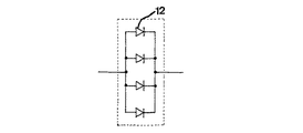
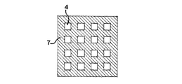
2 ドリフト層
4 エミッタ層領域
5 金属層
7 ドリフト層領域
9 金属層
11 グリッド部が開始する位置
Claims (22)
- SiCのジャンクション・バリア・ショットキ・ダイオードの温度依存性を制御する方法であって、
上記ダイオードを製造するときに、次のステップ、すなわち、
1) 上記材料からなる次の半導体層、すなわち、nまたはpの第1の導電型によって高くドープされた基体層(1)と、上記第1の導電型によって低くドープされたドリフト層(2)とを、各々の表面で、エピタキシャル成長するステップと、
2) ダイオードのグリッド部を形成するために、上記基体層から垂直方向に距離をおいた位置に、上記ドリフト層にドープされたエミッタ層領域(4)を形成するように、第1の導電型と逆であるnまたはpの第2の導電型のドーパントを、上記ドリフト層において横方向に間隔をおいた領域に導入し、上記グリッド部は、上記ドープされたエミッタ層領域(4)およびそこに隣接したドリフト層領域(7)を含んでいると共に、上記ドリフト層(2)まで延在しているステップと、
3) 上記ドリフト層領域(7)にショットキ接続を形成するために、ドリフト層の表面に、金属層(5)を塗布すると共に、そこに接触を形成するために、エミッタ層領域(4)の少なくとも一つの表面に、金属層(5)を塗布するステップと
が実行され、
少なくとも上記ステップ2)は、上記グリッド部(4,7)の全オン状態抵抗が、ダイオードの全オン状態抵抗の少なくとも80%を担うように、上記ダイオードのグリッド部(4,7)のオン状態抵抗を調節するために実行され、そのことによって、ダイオードの温度係数が、負から正に移行するダイオードの動作のクロスオーバー点を決定するダイオードのオン状態抵抗に関与することを特徴とするSiCのジャンクション・バリア・ショットキ・ダイオードの温度依存性を制御する方法。 - 請求項1に記載の方法において、
1700[V]以下の電圧阻止能力を有するダイオードが製造されることを特徴とする方法。 - 請求項1に記載の方法において、
600−1700[V]の電圧阻止能力を有するダイオードが製造されることを特徴とする方法。 - 請求項1に記載の方法において、
600−3500[V]の電圧阻止能力を有するダイオードが製造されることを特徴とする方法。 - 請求項1に記載の方法において、
600[V]と1500[V]との間の電圧阻止能力を有するダイオードが製造されることを特徴とする方法。 - 請求項1乃至5のいずれか1つに記載の方法において、
上記ステップ1)で、上記ダイオードの上記グリッド部(4,7)の抵抗は、後にステップ2)で上記グリッド部の一部となるドリフト層領域(7)の不純物添加濃度を調節することにより、調節されることを特徴とする方法。 - 請求項6に記載の方法において、
ステップ1)で、上記グリッド部のエミッタ層領域(4)を分離する上記ドリフト層領域(7)の不純物添加濃度は、上記ドリフト層の他の部分よりも低く調整されており、その結果、上記ドリフト層の他の部分を同じ不純物添加濃度とした場合よりも、上記ダイオードの上記グリッド部の抵抗が増大していることを特徴とする方法。 - 請求項1乃至7のいずれか1つに記載の方法において、
ステップ2)では、上記ダイオードのトータル横断面に対する上記グリップ部の上記ドリフト層領域(7)の横断面の比は、上記グリッド部の抵抗を調整のために、2/3まで増大されていることを特徴とする方法。 - 請求項1乃至8のいずれか1つに記載の方法において、
ステップ1)では、上記ドリフト層(2)の不純物添加濃度は、ドリフト層の抵抗の低減およびダイオードの所定の電圧阻止性能でのダイオードのオン状態損失を低減するためのグリッド部なしのダイオードで許容されている最大の不純物添加濃度よりも高いことを特徴とする方法。 - 請求項1乃至9のいずれか1つに記載の方法において、
ドナーによってドープされたドリフト層(2)を有するダイオードが製造されることを特徴とする方法。 - 請求項9または10に記載の方法において、
上記ドリフト層の不純物添加濃度が、1017cm−3以上であることを特徴とする方法。 - 請求項10または11に記載の方法において、
p型エミッタ層領域(4)が、1017−1020cm−3の不純物添加濃度を与えられていることを特徴とする方法。 - 請求項7に記載の方法において、上記ドリフト層領域(7)は、1016cm−3よりも少ない不純物添加濃度を与えられていることを特徴とする方法。
- 請求項13に記載の方法において、上記ドリフト層領域(7)は、1014cm−3−5・1015cm−3の不純物添加濃度を与えられていることを特徴とする方法。
- 請求項13に記載の方法において、上記ドリフト層領域(7)は、5・1014cm−3−1015cm−3の不純物添加濃度を与えられていることを特徴とする方法。
- 半導体材料としてのSiCからなる基体層(1)を備え、上記基体層(1)は、第1導電型nまたはpによって高くドープされており、
また、上記基体層上に上記材料のエピタキシャルドリフト層(2)を備え、上記エピタキシャルドリフト層(2)は、上記第1導電型を有し、
また、上記エピタキシャルドリフト層の表面にグリッド部(4,7)を備え、上記グリッド部(4,7)は、上記基体(1)から垂直方向に間隔をおいて上記第1導電型とは反対の第2導電型nまたはpのドーパントがドープされたエミッタ層領域(4)を含むと共に、上記ドープされたエミッタ層領域(4)に隣接すると共に、上記ドリフト層(2)まで延在するドリフト層領域(7)を含み、
また、上記ドリフト層(2)上に金属層(5)を備え、上記金属層(5)は、上記ドリフト層領域(7)にショットキ接触すると共に、上記エミッタ層領域(4)の少なくとも一つに接触しており、
上記ダイオードは、1700[V]以下の電圧阻止能力を有し、上記グリッド部(4、7)のオン状態は、少なくともトータルオン状態抵抗の80%を担い、そのことによって、ダイオードの温度係数が、負から正に移行するダイオードの動作のクロスオーバー点を決定するダイオードのオン状態抵抗に寄与することを特徴とするジャンクション・バリア・ショットキ・ダイオード。 - 請求項16に記載のジャンクション・バリア・ショットキ・ダイオードにおいて、
上記ダイオードは、600V−1700Vの電圧阻止能力を有していることを特徴とするジャンクション・バリア・ショットキ・ダイオード。 - 請求項16または17に記載のジャンクション・バリア・ショットキ・ダイオードにおいて、
ドリフト層領域(7)は、上記ドリフト層(2)の不純物添加濃度よりも低い不純物添加濃度を有していることを特徴とするジャンクション・バリア・ショットキ・ダイオード。 - 請求項18に記載のジャンクション・バリア・ショットキ・ダイオードにおいて、
上記ドリフト層領域(7)は、1016cm−3より低い不純物添加濃度を有していることを特徴とするジャンクション・バリア・ショットキ・ダイオード。 - 請求項18に記載のジャンクション・バリア・ショットキ・ダイオードにおいて、
上記ドリフト層領域(7)は、1014cm−3−5・1015cm−3の不純物添加濃度を有していることを特徴とするジャンクション・バリア・ショットキ・ダイオード。 - 請求項18に記載のジャンクション・バリア・ショットキ・ダイオードにおいて、
上記ドリフト層領域(7)は、5・1014cm−3−1015cm−3の不純物添加濃度を有していることを特徴とするジャンクション・バリア・ショットキ・ダイオード。 - 請求項16に記載のジャンクション・バリア・ショットキ・ダイオードにおいて、
上記ダイオードのトータル横断面積に対する上記ドリフト層領域(7)の横断面積の関係は、上記グリッド部(4,7)のオン状態抵抗が、上記オン状態抵抗の少なくともかなりの部分を構成するように備えられることを特徴とするジャンクション・バリア・ショットキ・ダイオード。
Applications Claiming Priority (2)
| Application Number | Priority Date | Filing Date | Title |
|---|---|---|---|
| SE0101848A SE0101848D0 (sv) | 2001-05-25 | 2001-05-25 | A method concerning a junction barrier Schottky diode, such a diode and use thereof |
| SE0101848-0 | 2001-05-25 |
Related Parent Applications (1)
| Application Number | Title | Priority Date | Filing Date |
|---|---|---|---|
| JP2003502878A Division JP2004528728A (ja) | 2001-05-25 | 2002-05-24 | ジャンクション・バリア・ショットキ・ダイオードに関する方法と、そのダイオードおよびその使用方法 |
Publications (2)
| Publication Number | Publication Date |
|---|---|
| JP2010050468A true JP2010050468A (ja) | 2010-03-04 |
| JP5554042B2 JP5554042B2 (ja) | 2014-07-23 |
Family
ID=20284243
Family Applications (2)
| Application Number | Title | Priority Date | Filing Date |
|---|---|---|---|
| JP2003502878A Pending JP2004528728A (ja) | 2001-05-25 | 2002-05-24 | ジャンクション・バリア・ショットキ・ダイオードに関する方法と、そのダイオードおよびその使用方法 |
| JP2009230498A Expired - Lifetime JP5554042B2 (ja) | 2001-05-25 | 2009-10-02 | ジャンクション・バリア・ショットキ・ダイオードに関する方法と、そのダイオードおよびその使用方法 |
Family Applications Before (1)
| Application Number | Title | Priority Date | Filing Date |
|---|---|---|---|
| JP2003502878A Pending JP2004528728A (ja) | 2001-05-25 | 2002-05-24 | ジャンクション・バリア・ショットキ・ダイオードに関する方法と、そのダイオードおよびその使用方法 |
Country Status (4)
| Country | Link |
|---|---|
| EP (1) | EP1390973A1 (ja) |
| JP (2) | JP2004528728A (ja) |
| SE (1) | SE0101848D0 (ja) |
| WO (1) | WO2002099869A1 (ja) |
Cited By (3)
| Publication number | Priority date | Publication date | Assignee | Title |
|---|---|---|---|---|
| JP2012227501A (ja) * | 2011-04-06 | 2012-11-15 | Rohm Co Ltd | 半導体装置 |
| JP2013140824A (ja) * | 2011-12-28 | 2013-07-18 | Rohm Co Ltd | 半導体装置および半導体装置の製造方法 |
| US9331150B2 (en) | 2014-02-17 | 2016-05-03 | Kabushiki Kaisha Toshiba | Semiconductor device and method of manufacturing the same |
Families Citing this family (15)
| Publication number | Priority date | Publication date | Assignee | Title |
|---|---|---|---|---|
| SE0101848D0 (sv) * | 2001-05-25 | 2001-05-25 | Abb Research Ltd | A method concerning a junction barrier Schottky diode, such a diode and use thereof |
| DE10235198B4 (de) * | 2001-08-02 | 2011-08-11 | Fuji Electric Systems Co., Ltd. | Leistungs-Halbleitergleichrichter mit ringförmigen Gräben |
| JP2006352006A (ja) * | 2005-06-20 | 2006-12-28 | Sumitomo Electric Ind Ltd | 整流素子およびその製造方法 |
| DE102005046707B3 (de) * | 2005-09-29 | 2007-05-03 | Siced Electronics Development Gmbh & Co. Kg | SiC-PN-Leistungsdiode |
| WO2007133123A1 (en) * | 2006-05-12 | 2007-11-22 | Cree Sweden Ab | A semiconductor device |
| JP4939839B2 (ja) * | 2006-05-30 | 2012-05-30 | 株式会社東芝 | 半導体整流素子 |
| US7728403B2 (en) * | 2006-05-31 | 2010-06-01 | Cree Sweden Ab | Semiconductor device |
| CN101431020B (zh) * | 2007-11-09 | 2010-09-08 | 上海华虹Nec电子有限公司 | T型多晶硅栅电极的制备方法 |
| EP2154726A3 (en) * | 2008-08-14 | 2010-05-26 | Acreo AB | A method for producing a JBS diode |
| DE102011003961B4 (de) | 2011-02-11 | 2023-07-27 | Robert Bosch Gmbh | Trench-Schottkydiode |
| JP2011142355A (ja) * | 2011-04-21 | 2011-07-21 | Sumitomo Electric Ind Ltd | 整流素子 |
| JP2017045901A (ja) * | 2015-08-27 | 2017-03-02 | トヨタ自動車株式会社 | 還流ダイオードと車載用電源装置 |
| JP6767705B2 (ja) | 2016-04-28 | 2020-10-14 | パナソニックIpマネジメント株式会社 | 半導体素子 |
| CN109148605B (zh) * | 2017-06-19 | 2022-02-18 | 比亚迪半导体股份有限公司 | 快恢复二极管及制备方法、电子设备 |
| JP6827433B2 (ja) | 2018-03-02 | 2021-02-10 | 株式会社東芝 | 半導体装置 |
Citations (6)
| Publication number | Priority date | Publication date | Assignee | Title |
|---|---|---|---|---|
| JPH02137368A (ja) * | 1988-11-18 | 1990-05-25 | Toshiba Corp | 半導体整流装置 |
| JPH07263716A (ja) * | 1994-03-17 | 1995-10-13 | Ricoh Co Ltd | 半導体装置 |
| JPH10321879A (ja) * | 1997-05-22 | 1998-12-04 | Hitachi Ltd | 炭化けい素ダイオード |
| WO1999033160A1 (de) * | 1997-12-19 | 1999-07-01 | Siemens Aktiengesellschaft | Elektrische schaltungsanordnung zur transformation von magnetischer feldenergie in elektrische feldenergie |
| JP2000512075A (ja) * | 1996-05-13 | 2000-09-12 | ノース・キャロライナ・ステイト・ユニヴァーシティ | ショットキー障壁整流器およびその製造方法 |
| JP2004528728A (ja) * | 2001-05-25 | 2004-09-16 | クリー・インコーポレーテッド | ジャンクション・バリア・ショットキ・ダイオードに関する方法と、そのダイオードおよびその使用方法 |
Family Cites Families (4)
| Publication number | Priority date | Publication date | Assignee | Title |
|---|---|---|---|---|
| JP2667477B2 (ja) * | 1988-12-02 | 1997-10-27 | 株式会社東芝 | ショットキーバリアダイオード |
| JPH0750791B2 (ja) * | 1989-09-20 | 1995-05-31 | 株式会社日立製作所 | 半導体整流ダイオード及びそれを使つた電源装置並びに電子計算機 |
| SE9700141D0 (sv) * | 1997-01-20 | 1997-01-20 | Abb Research Ltd | A schottky diode of SiC and a method for production thereof |
| JP4088852B2 (ja) * | 1998-09-21 | 2008-05-21 | 関西電力株式会社 | SiCショットキーダイオード |
-
2001
- 2001-05-25 SE SE0101848A patent/SE0101848D0/xx unknown
-
2002
- 2002-05-24 JP JP2003502878A patent/JP2004528728A/ja active Pending
- 2002-05-24 WO PCT/SE2002/000994 patent/WO2002099869A1/en not_active Ceased
- 2002-05-24 EP EP02736346A patent/EP1390973A1/en not_active Ceased
-
2009
- 2009-10-02 JP JP2009230498A patent/JP5554042B2/ja not_active Expired - Lifetime
Patent Citations (7)
| Publication number | Priority date | Publication date | Assignee | Title |
|---|---|---|---|---|
| JPH02137368A (ja) * | 1988-11-18 | 1990-05-25 | Toshiba Corp | 半導体整流装置 |
| JPH07263716A (ja) * | 1994-03-17 | 1995-10-13 | Ricoh Co Ltd | 半導体装置 |
| JP2000512075A (ja) * | 1996-05-13 | 2000-09-12 | ノース・キャロライナ・ステイト・ユニヴァーシティ | ショットキー障壁整流器およびその製造方法 |
| JPH10321879A (ja) * | 1997-05-22 | 1998-12-04 | Hitachi Ltd | 炭化けい素ダイオード |
| WO1999033160A1 (de) * | 1997-12-19 | 1999-07-01 | Siemens Aktiengesellschaft | Elektrische schaltungsanordnung zur transformation von magnetischer feldenergie in elektrische feldenergie |
| JP2001527377A (ja) * | 1997-12-19 | 2001-12-25 | シーメンス アクチエンゲゼルシヤフト | 磁場エネルギーを電場エネルギーに変換するための電気回路装置 |
| JP2004528728A (ja) * | 2001-05-25 | 2004-09-16 | クリー・インコーポレーテッド | ジャンクション・バリア・ショットキ・ダイオードに関する方法と、そのダイオードおよびその使用方法 |
Cited By (3)
| Publication number | Priority date | Publication date | Assignee | Title |
|---|---|---|---|---|
| JP2012227501A (ja) * | 2011-04-06 | 2012-11-15 | Rohm Co Ltd | 半導体装置 |
| JP2013140824A (ja) * | 2011-12-28 | 2013-07-18 | Rohm Co Ltd | 半導体装置および半導体装置の製造方法 |
| US9331150B2 (en) | 2014-02-17 | 2016-05-03 | Kabushiki Kaisha Toshiba | Semiconductor device and method of manufacturing the same |
Also Published As
| Publication number | Publication date |
|---|---|
| SE0101848D0 (sv) | 2001-05-25 |
| EP1390973A1 (en) | 2004-02-25 |
| WO2002099869A1 (en) | 2002-12-12 |
| JP5554042B2 (ja) | 2014-07-23 |
| JP2004528728A (ja) | 2004-09-16 |
Similar Documents
| Publication | Publication Date | Title |
|---|---|---|
| JP5554042B2 (ja) | ジャンクション・バリア・ショットキ・ダイオードに関する方法と、そのダイオードおよびその使用方法 | |
| US6524900B2 (en) | Method concerning a junction barrier Schottky diode, such a diode and use thereof | |
| KR100937276B1 (ko) | 반도체 디바이스 및 그 제조 방법 | |
| CN101223647B (zh) | 具有抑制的少数载流子注入的碳化硅结势垒肖特基二极管 | |
| KR101434687B1 (ko) | 접합 배리어 쇼트키 정류기들 및 그의 제조 방법 | |
| US8653534B2 (en) | Junction Barrier Schottky diodes with current surge capability | |
| KR101494935B1 (ko) | 메사 스텝들을 포함하는 버퍼층들 및 메사 구조들을 가지는 전력 반도체 장치들 | |
| KR20190072631A (ko) | 게이트 트렌치들 및 매립된 종단 구조체들을 갖는 전력 반도체 디바이스들 및 관련 방법들 | |
| US9972677B2 (en) | Methods of forming power semiconductor devices having superjunction structures with pillars having implanted sidewalls | |
| US6674152B2 (en) | Bipolar diode | |
| WO2009091695A1 (en) | Junction barrier schottky diode with highly-doped channel region and methods | |
| JP2004528728A5 (ja) | ||
| JP4972090B2 (ja) | 半導体装置およびその製造方法 | |
| WO2019053204A1 (en) | POWER SUPPLY PATTERN WITH HIGH CURRENT CAPACITY | |
| US5674765A (en) | Method for producing a semiconductor device by the use of an implanting step | |
| EP0890187B1 (en) | A method for producing a semiconductor device by the use of an implanting step |
Legal Events
| Date | Code | Title | Description |
|---|---|---|---|
| RD04 | Notification of resignation of power of attorney |
Free format text: JAPANESE INTERMEDIATE CODE: A7424 Effective date: 20110119 |
|
| RD02 | Notification of acceptance of power of attorney |
Free format text: JAPANESE INTERMEDIATE CODE: A7422 Effective date: 20110119 |
|
| A977 | Report on retrieval |
Free format text: JAPANESE INTERMEDIATE CODE: A971007 Effective date: 20120511 |
|
| A131 | Notification of reasons for refusal |
Free format text: JAPANESE INTERMEDIATE CODE: A131 Effective date: 20120703 |
|
| A601 | Written request for extension of time |
Free format text: JAPANESE INTERMEDIATE CODE: A601 Effective date: 20121003 |
|
| A602 | Written permission of extension of time |
Free format text: JAPANESE INTERMEDIATE CODE: A602 Effective date: 20121009 |
|
| A601 | Written request for extension of time |
Free format text: JAPANESE INTERMEDIATE CODE: A601 Effective date: 20121105 |
|
| A602 | Written permission of extension of time |
Free format text: JAPANESE INTERMEDIATE CODE: A602 Effective date: 20121108 |
|
| A601 | Written request for extension of time |
Free format text: JAPANESE INTERMEDIATE CODE: A601 Effective date: 20121203 |
|
| A602 | Written permission of extension of time |
Free format text: JAPANESE INTERMEDIATE CODE: A602 Effective date: 20121206 |
|
| A521 | Request for written amendment filed |
Free format text: JAPANESE INTERMEDIATE CODE: A523 Effective date: 20130104 |
|
| A02 | Decision of refusal |
Free format text: JAPANESE INTERMEDIATE CODE: A02 Effective date: 20130903 |
|
| A521 | Request for written amendment filed |
Free format text: JAPANESE INTERMEDIATE CODE: A523 Effective date: 20140106 |
|
| A911 | Transfer to examiner for re-examination before appeal (zenchi) |
Free format text: JAPANESE INTERMEDIATE CODE: A911 Effective date: 20140220 |
|
| TRDD | Decision of grant or rejection written | ||
| A01 | Written decision to grant a patent or to grant a registration (utility model) |
Free format text: JAPANESE INTERMEDIATE CODE: A01 Effective date: 20140502 |
|
| A61 | First payment of annual fees (during grant procedure) |
Free format text: JAPANESE INTERMEDIATE CODE: A61 Effective date: 20140528 |
|
| R150 | Certificate of patent or registration of utility model |
Ref document number: 5554042 Country of ref document: JP Free format text: JAPANESE INTERMEDIATE CODE: R150 |
|
| R250 | Receipt of annual fees |
Free format text: JAPANESE INTERMEDIATE CODE: R250 |
|
| R250 | Receipt of annual fees |
Free format text: JAPANESE INTERMEDIATE CODE: R250 |
|
| R250 | Receipt of annual fees |
Free format text: JAPANESE INTERMEDIATE CODE: R250 |
|
| R250 | Receipt of annual fees |
Free format text: JAPANESE INTERMEDIATE CODE: R250 |
|
| R250 | Receipt of annual fees |
Free format text: JAPANESE INTERMEDIATE CODE: R250 |
|
| EXPY | Cancellation because of completion of term |