JP2010040910A - Ledモジュール - Google Patents
Ledモジュール Download PDFInfo
- Publication number
- JP2010040910A JP2010040910A JP2008204129A JP2008204129A JP2010040910A JP 2010040910 A JP2010040910 A JP 2010040910A JP 2008204129 A JP2008204129 A JP 2008204129A JP 2008204129 A JP2008204129 A JP 2008204129A JP 2010040910 A JP2010040910 A JP 2010040910A
- Authority
- JP
- Japan
- Prior art keywords
- curve
- led chip
- led module
- led
- irradiation
- Prior art date
- Legal status (The legal status is an assumption and is not a legal conclusion. Google has not performed a legal analysis and makes no representation as to the accuracy of the status listed.)
- Granted
Links
Images


Classifications
-
- H—ELECTRICITY
- H01—ELECTRIC ELEMENTS
- H01L—SEMICONDUCTOR DEVICES NOT COVERED BY CLASS H10
- H01L2224/00—Indexing scheme for arrangements for connecting or disconnecting semiconductor or solid-state bodies and methods related thereto as covered by H01L24/00
- H01L2224/01—Means for bonding being attached to, or being formed on, the surface to be connected, e.g. chip-to-package, die-attach, "first-level" interconnects; Manufacturing methods related thereto
- H01L2224/42—Wire connectors; Manufacturing methods related thereto
- H01L2224/47—Structure, shape, material or disposition of the wire connectors after the connecting process
- H01L2224/48—Structure, shape, material or disposition of the wire connectors after the connecting process of an individual wire connector
- H01L2224/4805—Shape
- H01L2224/4809—Loop shape
- H01L2224/48091—Arched
-
- H—ELECTRICITY
- H01—ELECTRIC ELEMENTS
- H01L—SEMICONDUCTOR DEVICES NOT COVERED BY CLASS H10
- H01L2224/00—Indexing scheme for arrangements for connecting or disconnecting semiconductor or solid-state bodies and methods related thereto as covered by H01L24/00
- H01L2224/01—Means for bonding being attached to, or being formed on, the surface to be connected, e.g. chip-to-package, die-attach, "first-level" interconnects; Manufacturing methods related thereto
- H01L2224/42—Wire connectors; Manufacturing methods related thereto
- H01L2224/47—Structure, shape, material or disposition of the wire connectors after the connecting process
- H01L2224/48—Structure, shape, material or disposition of the wire connectors after the connecting process of an individual wire connector
- H01L2224/481—Disposition
- H01L2224/48151—Connecting between a semiconductor or solid-state body and an item not being a semiconductor or solid-state body, e.g. chip-to-substrate, chip-to-passive
- H01L2224/48221—Connecting between a semiconductor or solid-state body and an item not being a semiconductor or solid-state body, e.g. chip-to-substrate, chip-to-passive the body and the item being stacked
- H01L2224/48245—Connecting between a semiconductor or solid-state body and an item not being a semiconductor or solid-state body, e.g. chip-to-substrate, chip-to-passive the body and the item being stacked the item being metallic
- H01L2224/48247—Connecting between a semiconductor or solid-state body and an item not being a semiconductor or solid-state body, e.g. chip-to-substrate, chip-to-passive the body and the item being stacked the item being metallic connecting the wire to a bond pad of the item
Abstract
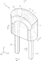
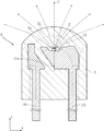
【解決手段】LEDチップ2と、LEDチップ2を覆い、かつLEDチップ2の照射軸Irが延びるz方向照射側に膨出した出射面3aを有する透光樹脂3と、を備えるLEDモジュールAであって、出射面3aは、照射軸Irを含み、かつz方向とx方向とによって構成される平面において、z方向照射側に膨出する曲線31に沿って、照射軸Irを含み、かつz方向とy方向とによって構成される平面において、z方向照射側に膨出する曲線32を移動させることによって得られる曲面とされており、曲線31は、その平均曲率が第2曲線32の平均曲率よりも小である。
【選択図】 図1
Description
Ir 照射軸
O1 (第1曲線の)中心
O2 (第2曲線の)中心
x (第2)方向
y (第3)方向
z (第1)方向
1A,1B リード
2 LEDチップ
3 透光樹脂
3a 出射面
31 (第1)曲線
32 (第2)曲線
Claims (5)
- LEDチップと、
上記LEDチップを覆い、かつ上記LEDチップの照射軸が延びる第1方向照射側に膨出した出射面を有する透光樹脂と、
を備えるLEDモジュールであって、
上記出射面は、
上記照射軸を含み、かつ上記第1方向と上記第1方向と直角である第2方向とによって構成される平面において、上記第1方向照射側に膨出する第1曲線に沿って、
上記照射軸を含み、かつ上記第1方向と上記第1および第2方向と直角である第3方向とによって構成される平面において、上記第1方向照射側に膨出する第2曲線を、移動させることによって得られる曲面とされており、
上記第1曲線は、その平均曲率が上記第2曲線の平均曲率よりも小であることを特徴とする、LEDモジュール。 - 上記第1曲線は、円弧である、請求項1に記載のLEDモジュール。
- 上記LEDチップは、上記第1曲線の中心と上記出射面との間に配置されている、請求項2に記載のLEDモジュール。
- 上記第2曲線は、円弧である、請求項1ないし3のいずれかに記載のLEDモジュール。
- 上記LEDチップは、上記出射面に対して上記第2曲線の中心よりも離れた位置に配置されている、請求項4に記載のLEDモジュール。
Priority Applications (1)
| Application Number | Priority Date | Filing Date | Title |
|---|---|---|---|
| JP2008204129A JP5384871B2 (ja) | 2008-08-07 | 2008-08-07 | Ledモジュール |
Applications Claiming Priority (1)
| Application Number | Priority Date | Filing Date | Title |
|---|---|---|---|
| JP2008204129A JP5384871B2 (ja) | 2008-08-07 | 2008-08-07 | Ledモジュール |
Publications (2)
| Publication Number | Publication Date |
|---|---|
| JP2010040910A true JP2010040910A (ja) | 2010-02-18 |
| JP5384871B2 JP5384871B2 (ja) | 2014-01-08 |
Family
ID=42013109
Family Applications (1)
| Application Number | Title | Priority Date | Filing Date |
|---|---|---|---|
| JP2008204129A Active JP5384871B2 (ja) | 2008-08-07 | 2008-08-07 | Ledモジュール |
Country Status (1)
| Country | Link |
|---|---|
| JP (1) | JP5384871B2 (ja) |
Cited By (1)
| Publication number | Priority date | Publication date | Assignee | Title |
|---|---|---|---|---|
| JP2011204433A (ja) * | 2010-03-25 | 2011-10-13 | Toshiba Lighting & Technology Corp | 航空障害灯 |
Citations (8)
| Publication number | Priority date | Publication date | Assignee | Title |
|---|---|---|---|---|
| JPH02224378A (ja) * | 1989-02-27 | 1990-09-06 | Hamamatsu Photonics Kk | 発光素子 |
| JPH05275751A (ja) * | 1992-03-26 | 1993-10-22 | Rohm Co Ltd | 発光ダイオード |
| JPH0715043A (ja) * | 1993-06-25 | 1995-01-17 | Toshiba Corp | Ledランプ |
| JPH08250772A (ja) * | 1996-02-23 | 1996-09-27 | Rohm Co Ltd | 発光ダイオード |
| JPH1022529A (ja) * | 1996-07-03 | 1998-01-23 | Nichia Chem Ind Ltd | 発光ダイオード及びそれを用いた表示装置 |
| JPH11154766A (ja) * | 1997-09-22 | 1999-06-08 | Nichia Chem Ind Ltd | 発光ダイオード及びそれを用いた信号機 |
| JP2001077427A (ja) * | 1999-08-31 | 2001-03-23 | Nichia Chem Ind Ltd | 発光ダイオード及びそれを用いた表示装置 |
| JP2006196931A (ja) * | 2006-04-21 | 2006-07-27 | Toshiba Corp | レンズ一体型発光素子 |
-
2008
- 2008-08-07 JP JP2008204129A patent/JP5384871B2/ja active Active
Patent Citations (8)
| Publication number | Priority date | Publication date | Assignee | Title |
|---|---|---|---|---|
| JPH02224378A (ja) * | 1989-02-27 | 1990-09-06 | Hamamatsu Photonics Kk | 発光素子 |
| JPH05275751A (ja) * | 1992-03-26 | 1993-10-22 | Rohm Co Ltd | 発光ダイオード |
| JPH0715043A (ja) * | 1993-06-25 | 1995-01-17 | Toshiba Corp | Ledランプ |
| JPH08250772A (ja) * | 1996-02-23 | 1996-09-27 | Rohm Co Ltd | 発光ダイオード |
| JPH1022529A (ja) * | 1996-07-03 | 1998-01-23 | Nichia Chem Ind Ltd | 発光ダイオード及びそれを用いた表示装置 |
| JPH11154766A (ja) * | 1997-09-22 | 1999-06-08 | Nichia Chem Ind Ltd | 発光ダイオード及びそれを用いた信号機 |
| JP2001077427A (ja) * | 1999-08-31 | 2001-03-23 | Nichia Chem Ind Ltd | 発光ダイオード及びそれを用いた表示装置 |
| JP2006196931A (ja) * | 2006-04-21 | 2006-07-27 | Toshiba Corp | レンズ一体型発光素子 |
Cited By (1)
| Publication number | Priority date | Publication date | Assignee | Title |
|---|---|---|---|---|
| JP2011204433A (ja) * | 2010-03-25 | 2011-10-13 | Toshiba Lighting & Technology Corp | 航空障害灯 |
Also Published As
| Publication number | Publication date |
|---|---|
| JP5384871B2 (ja) | 2014-01-08 |
Similar Documents
| Publication | Publication Date | Title |
|---|---|---|
| TWI446568B (zh) | 半導體發光裝置 | |
| KR101090575B1 (ko) | 반도체 발광 장치 | |
| JP6080053B2 (ja) | 発光モジュール | |
| JP2013115088A (ja) | 半導体発光装置 | |
| JP5236406B2 (ja) | 半導体発光モジュールおよびその製造方法 | |
| JP2013143430A (ja) | 半導体発光装置及びそれを用いた照明装置 | |
| JP2009246343A (ja) | 半導体発光装置およびその製造方法 | |
| JP2008251938A (ja) | 半導体発光装置 | |
| JP2013115116A (ja) | Ledモジュール | |
| JP2010516041A (ja) | 光源 | |
| JP2009099771A (ja) | 半導体発光モジュール | |
| JP2009182085A (ja) | 発光装置 | |
| JP2015056649A (ja) | 発光装置 | |
| JP5275140B2 (ja) | 照明装置及び発光装置 | |
| JP5384871B2 (ja) | Ledモジュール | |
| JP2020120118A (ja) | 半導体装置 | |
| JP4877239B2 (ja) | 発光装置の製造方法 | |
| JP2016213453A (ja) | Ledモジュール、および、それを用いたランプ | |
| JP5976406B2 (ja) | 半導体発光装置 | |
| JP6087098B2 (ja) | 光源装置、ledランプ、および液晶表示装置 | |
| JP6064415B2 (ja) | 発光装置 | |
| JP5049148B2 (ja) | 半導体発光モジュールおよびこれを用いた画像読取装置 | |
| JP5049154B2 (ja) | 半導体発光モジュールおよびこれを用いた画像読取装置 | |
| JP5878226B2 (ja) | 半導体発光装置 | |
| JP6307584B2 (ja) | 半導体発光装置 |
Legal Events
| Date | Code | Title | Description |
|---|---|---|---|
| A621 | Written request for application examination |
Free format text: JAPANESE INTERMEDIATE CODE: A621 Effective date: 20110804 |
|
| A977 | Report on retrieval |
Free format text: JAPANESE INTERMEDIATE CODE: A971007 Effective date: 20120912 |
|
| A131 | Notification of reasons for refusal |
Free format text: JAPANESE INTERMEDIATE CODE: A131 Effective date: 20120925 |
|
| A521 | Request for written amendment filed |
Free format text: JAPANESE INTERMEDIATE CODE: A523 Effective date: 20121120 |
|
| A02 | Decision of refusal |
Free format text: JAPANESE INTERMEDIATE CODE: A02 Effective date: 20130115 |
|
| A521 | Request for written amendment filed |
Free format text: JAPANESE INTERMEDIATE CODE: A523 Effective date: 20130415 |
|
| A911 | Transfer to examiner for re-examination before appeal (zenchi) |
Free format text: JAPANESE INTERMEDIATE CODE: A911 Effective date: 20130422 |
|
| A912 | Re-examination (zenchi) completed and case transferred to appeal board |
Free format text: JAPANESE INTERMEDIATE CODE: A912 Effective date: 20130517 |
|
| A61 | First payment of annual fees (during grant procedure) |
Free format text: JAPANESE INTERMEDIATE CODE: A61 Effective date: 20131003 |
|
| R150 | Certificate of patent or registration of utility model |
Ref document number: 5384871 Country of ref document: JP Free format text: JAPANESE INTERMEDIATE CODE: R150 Free format text: JAPANESE INTERMEDIATE CODE: R150 |
|
| R250 | Receipt of annual fees |
Free format text: JAPANESE INTERMEDIATE CODE: R250 |
|
| R250 | Receipt of annual fees |
Free format text: JAPANESE INTERMEDIATE CODE: R250 |
|
| R250 | Receipt of annual fees |
Free format text: JAPANESE INTERMEDIATE CODE: R250 |
|
| R250 | Receipt of annual fees |
Free format text: JAPANESE INTERMEDIATE CODE: R250 |
|
| R250 | Receipt of annual fees |
Free format text: JAPANESE INTERMEDIATE CODE: R250 |