JP5976406B2 - 半導体発光装置 - Google Patents
半導体発光装置 Download PDFInfo
- Publication number
- JP5976406B2 JP5976406B2 JP2012131691A JP2012131691A JP5976406B2 JP 5976406 B2 JP5976406 B2 JP 5976406B2 JP 2012131691 A JP2012131691 A JP 2012131691A JP 2012131691 A JP2012131691 A JP 2012131691A JP 5976406 B2 JP5976406 B2 JP 5976406B2
- Authority
- JP
- Japan
- Prior art keywords
- light
- led device
- led
- groove
- sealing member
- Prior art date
- Legal status (The legal status is an assumption and is not a legal conclusion. Google has not performed a legal analysis and makes no representation as to the accuracy of the status listed.)
- Active
Links
Images


Classifications
-
- H—ELECTRICITY
- H01—ELECTRIC ELEMENTS
- H01L—SEMICONDUCTOR DEVICES NOT COVERED BY CLASS H10
- H01L2224/00—Indexing scheme for arrangements for connecting or disconnecting semiconductor or solid-state bodies and methods related thereto as covered by H01L24/00
- H01L2224/01—Means for bonding being attached to, or being formed on, the surface to be connected, e.g. chip-to-package, die-attach, "first-level" interconnects; Manufacturing methods related thereto
- H01L2224/10—Bump connectors; Manufacturing methods related thereto
- H01L2224/15—Structure, shape, material or disposition of the bump connectors after the connecting process
- H01L2224/16—Structure, shape, material or disposition of the bump connectors after the connecting process of an individual bump connector
- H01L2224/161—Disposition
- H01L2224/16151—Disposition the bump connector connecting between a semiconductor or solid-state body and an item not being a semiconductor or solid-state body, e.g. chip-to-substrate, chip-to-passive
- H01L2224/16221—Disposition the bump connector connecting between a semiconductor or solid-state body and an item not being a semiconductor or solid-state body, e.g. chip-to-substrate, chip-to-passive the body and the item being stacked
- H01L2224/16225—Disposition the bump connector connecting between a semiconductor or solid-state body and an item not being a semiconductor or solid-state body, e.g. chip-to-substrate, chip-to-passive the body and the item being stacked the item being non-metallic, e.g. insulating substrate with or without metallisation
-
- H—ELECTRICITY
- H01—ELECTRIC ELEMENTS
- H01L—SEMICONDUCTOR DEVICES NOT COVERED BY CLASS H10
- H01L2224/00—Indexing scheme for arrangements for connecting or disconnecting semiconductor or solid-state bodies and methods related thereto as covered by H01L24/00
- H01L2224/01—Means for bonding being attached to, or being formed on, the surface to be connected, e.g. chip-to-package, die-attach, "first-level" interconnects; Manufacturing methods related thereto
- H01L2224/42—Wire connectors; Manufacturing methods related thereto
- H01L2224/47—Structure, shape, material or disposition of the wire connectors after the connecting process
- H01L2224/48—Structure, shape, material or disposition of the wire connectors after the connecting process of an individual wire connector
- H01L2224/4805—Shape
- H01L2224/4809—Loop shape
- H01L2224/48091—Arched
-
- H—ELECTRICITY
- H01—ELECTRIC ELEMENTS
- H01L—SEMICONDUCTOR DEVICES NOT COVERED BY CLASS H10
- H01L2224/00—Indexing scheme for arrangements for connecting or disconnecting semiconductor or solid-state bodies and methods related thereto as covered by H01L24/00
- H01L2224/01—Means for bonding being attached to, or being formed on, the surface to be connected, e.g. chip-to-package, die-attach, "first-level" interconnects; Manufacturing methods related thereto
- H01L2224/42—Wire connectors; Manufacturing methods related thereto
- H01L2224/47—Structure, shape, material or disposition of the wire connectors after the connecting process
- H01L2224/48—Structure, shape, material or disposition of the wire connectors after the connecting process of an individual wire connector
- H01L2224/484—Connecting portions
- H01L2224/48463—Connecting portions the connecting portion on the bonding area of the semiconductor or solid-state body being a ball bond
- H01L2224/48465—Connecting portions the connecting portion on the bonding area of the semiconductor or solid-state body being a ball bond the other connecting portion not on the bonding area being a wedge bond, i.e. ball-to-wedge, regular stitch
-
- H—ELECTRICITY
- H01—ELECTRIC ELEMENTS
- H01L—SEMICONDUCTOR DEVICES NOT COVERED BY CLASS H10
- H01L2224/00—Indexing scheme for arrangements for connecting or disconnecting semiconductor or solid-state bodies and methods related thereto as covered by H01L24/00
- H01L2224/93—Batch processes
- H01L2224/95—Batch processes at chip-level, i.e. with connecting carried out on a plurality of singulated devices, i.e. on diced chips
- H01L2224/97—Batch processes at chip-level, i.e. with connecting carried out on a plurality of singulated devices, i.e. on diced chips the devices being connected to a common substrate, e.g. interposer, said common substrate being separable into individual assemblies after connecting
Landscapes
- Led Device Packages (AREA)
Description
、LEDダイ30を封止部材13が被覆し、封止部材13を白色部材11,12が取り囲んでいる様子が示されている。ここで白色部材12と同じ材料からなる白色部材11は、図1(b)と異なり、上下方向の幅が200μm程度であり、左右方向の幅が100μm程度の白色部材12よりも厚くなっている。このときサファイヤ基板31上の封止部材13の厚さは200μm程度になっている。
ついて描いているので、奥側にV溝63の高い方の稜線が見えることから、封止部材62中に水平方向の線が現れている。
11,12,65…白色部材、
13,54,62…封止部材、
14,55…回路基板、
15,16…外部接続電極、
30…LEDダイ(半導体発光素子)、
31…サファイヤ基板、
32…n型半導体層、
33…p型半導体層、
34…絶縁膜、
35a…p側電極、
35b…n側電極、
36,38…内部接続電極、
37,39…スルーホール電極、
51,52…配光分布、
53,71…実装基板、
56…参照例のLED装置、
61…大判基板、
63…V溝、
64…角溝、
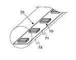
70…ライン光源、
72…チューブ状の拡散部材、
L1〜L7…光線。
Claims (3)
- 回路基板上にLEDダイを実装し、該LEDダイを透光性の封止部材で被覆した半導体発光装置において、
前記封止部材は上部に溝を備え、
前記溝は前記封止部材の上部全体に亘り、中心部が最も低く、白色部材が充填され、
前記白色部材は前記溝と直交する方向の端部から上方に光が漏れ出し、
前記溝と直交する前記封止部材の一対の側面に白色部材を備えている
ことを特徴とする半導体発光装置。 - 前記溝がV溝であることを特徴とする請求項1に記載の半導体発光装置。
- 前記LEDダイがフリップチップ実装されていることを特徴とする請求項1又は2に記載の半導体発光装置。
Priority Applications (1)
| Application Number | Priority Date | Filing Date | Title |
|---|---|---|---|
| JP2012131691A JP5976406B2 (ja) | 2012-06-11 | 2012-06-11 | 半導体発光装置 |
Applications Claiming Priority (1)
| Application Number | Priority Date | Filing Date | Title |
|---|---|---|---|
| JP2012131691A JP5976406B2 (ja) | 2012-06-11 | 2012-06-11 | 半導体発光装置 |
Publications (3)
| Publication Number | Publication Date |
|---|---|
| JP2013258175A JP2013258175A (ja) | 2013-12-26 |
| JP2013258175A5 JP2013258175A5 (ja) | 2014-12-18 |
| JP5976406B2 true JP5976406B2 (ja) | 2016-08-23 |
Family
ID=49954394
Family Applications (1)
| Application Number | Title | Priority Date | Filing Date |
|---|---|---|---|
| JP2012131691A Active JP5976406B2 (ja) | 2012-06-11 | 2012-06-11 | 半導体発光装置 |
Country Status (1)
| Country | Link |
|---|---|
| JP (1) | JP5976406B2 (ja) |
Families Citing this family (3)
| Publication number | Priority date | Publication date | Assignee | Title |
|---|---|---|---|---|
| DE102013104840A1 (de) | 2013-05-10 | 2014-11-13 | Osram Opto Semiconductors Gmbh | Strahlungsemittierendes Halbleiterbauelement und Verfahren zur Herstellung von strahlungsemittierenden Halbleiterbauelementen |
| TWI583028B (zh) * | 2016-02-05 | 2017-05-11 | 行家光電股份有限公司 | 具有光形調整結構之發光裝置及其製造方法 |
| JP7295437B2 (ja) * | 2019-11-29 | 2023-06-21 | 日亜化学工業株式会社 | 発光装置 |
Family Cites Families (4)
| Publication number | Priority date | Publication date | Assignee | Title |
|---|---|---|---|---|
| JP2002170998A (ja) * | 2000-12-01 | 2002-06-14 | Sharp Corp | 半導体発光装置およびその製造方法 |
| JP4400786B2 (ja) * | 2004-06-11 | 2010-01-20 | シチズン電子株式会社 | 発光ダイオード |
| TW200943590A (en) * | 2008-01-22 | 2009-10-16 | Alps Electric Co Ltd | Led package and manufacturing method therefor |
| JP2009246353A (ja) * | 2008-03-10 | 2009-10-22 | Opt Link Co Ltd | Led低背光源装置及びled低背光源装置の製造方法 |
-
2012
- 2012-06-11 JP JP2012131691A patent/JP5976406B2/ja active Active
Also Published As
| Publication number | Publication date |
|---|---|
| JP2013258175A (ja) | 2013-12-26 |
Similar Documents
| Publication | Publication Date | Title |
|---|---|---|
| JP2013115088A (ja) | 半導体発光装置 | |
| JP6934712B2 (ja) | 半導体発光装置及び車両用灯具 | |
| JP2013143430A (ja) | 半導体発光装置及びそれを用いた照明装置 | |
| JP2014138176A (ja) | 半導体発光装置 | |
| US10497826B2 (en) | Light-emitting device and method of manufacturing the same | |
| JP2013118244A (ja) | 半導体発光装置及びそれを用いた照明装置 | |
| JP2008251618A (ja) | 発光ダイオード及びその製造方法 | |
| JP2006278924A (ja) | 半導体発光装置及び半導体発光ユニット | |
| US8366307B2 (en) | Semiconductor light emitting device | |
| KR101055081B1 (ko) | 발광 소자, 발광 소자 제조방법 및 백라이트 유닛 | |
| JP5976406B2 (ja) | 半導体発光装置 | |
| US20120009700A1 (en) | Method of manufacturing a led chip package structure | |
| US20150076541A1 (en) | Light-emitting device | |
| TW201525525A (zh) | 光學顯示系統 | |
| JP5286122B2 (ja) | 半導体発光装置および半導体発光装置の製造方法 | |
| JP2013149711A (ja) | 半導体発光装置 | |
| US20120001203A1 (en) | Led chip package structure | |
| TWI610470B (zh) | 發光二極體晶片級封裝結構、直下式背光模組及發光裝置的製造方法 | |
| JP2009283988A (ja) | 発光ダイオード | |
| JP6173794B2 (ja) | 半導体発光装置およびそれを用いた照明装置 | |
| TWI688128B (zh) | 發光二極體晶片級封裝結構及直下式背光模組 | |
| JP6087098B2 (ja) | 光源装置、ledランプ、および液晶表示装置 | |
| JP2009224376A (ja) | 側面型発光装置及びその製造方法 | |
| JP6847661B2 (ja) | 発光デバイス及びその形成方法 | |
| KR20120013795A (ko) | 발광소자 패키지 |
Legal Events
| Date | Code | Title | Description |
|---|---|---|---|
| A521 | Request for written amendment filed |
Free format text: JAPANESE INTERMEDIATE CODE: A523 Effective date: 20141030 |
|
| A621 | Written request for application examination |
Free format text: JAPANESE INTERMEDIATE CODE: A621 Effective date: 20141030 |
|
| A977 | Report on retrieval |
Free format text: JAPANESE INTERMEDIATE CODE: A971007 Effective date: 20150924 |
|
| A131 | Notification of reasons for refusal |
Free format text: JAPANESE INTERMEDIATE CODE: A131 Effective date: 20151006 |
|
| A521 | Request for written amendment filed |
Free format text: JAPANESE INTERMEDIATE CODE: A523 Effective date: 20151118 |
|
| A131 | Notification of reasons for refusal |
Free format text: JAPANESE INTERMEDIATE CODE: A131 Effective date: 20160510 |
|
| A521 | Request for written amendment filed |
Free format text: JAPANESE INTERMEDIATE CODE: A523 Effective date: 20160524 |
|
| TRDD | Decision of grant or rejection written | ||
| A01 | Written decision to grant a patent or to grant a registration (utility model) |
Free format text: JAPANESE INTERMEDIATE CODE: A01 Effective date: 20160705 |
|
| A61 | First payment of annual fees (during grant procedure) |
Free format text: JAPANESE INTERMEDIATE CODE: A61 Effective date: 20160720 |
|
| R150 | Certificate of patent or registration of utility model |
Ref document number: 5976406 Country of ref document: JP Free format text: JAPANESE INTERMEDIATE CODE: R150 |
|
| S533 | Written request for registration of change of name |
Free format text: JAPANESE INTERMEDIATE CODE: R313533 |
|
| R350 | Written notification of registration of transfer |
Free format text: JAPANESE INTERMEDIATE CODE: R350 |
|
| R250 | Receipt of annual fees |
Free format text: JAPANESE INTERMEDIATE CODE: R250 |
|
| R250 | Receipt of annual fees |
Free format text: JAPANESE INTERMEDIATE CODE: R250 |
|
| R250 | Receipt of annual fees |
Free format text: JAPANESE INTERMEDIATE CODE: R250 |