JP2010040887A - Carrying container for holding jig - Google Patents
Carrying container for holding jig Download PDFInfo
- Publication number
- JP2010040887A JP2010040887A JP2008203724A JP2008203724A JP2010040887A JP 2010040887 A JP2010040887 A JP 2010040887A JP 2008203724 A JP2008203724 A JP 2008203724A JP 2008203724 A JP2008203724 A JP 2008203724A JP 2010040887 A JP2010040887 A JP 2010040887A
- Authority
- JP
- Japan
- Prior art keywords
- container
- main body
- holding jig
- lid
- frustum
- Prior art date
- Legal status (The legal status is an assumption and is not a legal conclusion. Google has not performed a legal analysis and makes no representation as to the accuracy of the status listed.)
- Granted
Links
- 230000002093 peripheral effect Effects 0.000 claims description 34
- 238000005192 partition Methods 0.000 claims description 18
- 239000000758 substrate Substances 0.000 claims description 18
- 230000001105 regulatory effect Effects 0.000 abstract 1
- 235000012431 wafers Nutrition 0.000 description 44
- 238000000034 method Methods 0.000 description 10
- 239000000463 material Substances 0.000 description 6
- 239000004065 semiconductor Substances 0.000 description 4
- 238000003860 storage Methods 0.000 description 4
- 229920005989 resin Polymers 0.000 description 3
- 239000011347 resin Substances 0.000 description 3
- VYPSYNLAJGMNEJ-UHFFFAOYSA-N Silicium dioxide Chemical compound O=[Si]=O VYPSYNLAJGMNEJ-UHFFFAOYSA-N 0.000 description 2
- 230000003139 buffering effect Effects 0.000 description 2
- 239000012778 molding material Substances 0.000 description 2
- 238000000465 moulding Methods 0.000 description 2
- 229920000515 polycarbonate Polymers 0.000 description 2
- 239000004417 polycarbonate Substances 0.000 description 2
- 230000003014 reinforcing effect Effects 0.000 description 2
- 229910000838 Al alloy Inorganic materials 0.000 description 1
- YCKRFDGAMUMZLT-UHFFFAOYSA-N Fluorine atom Chemical compound [F] YCKRFDGAMUMZLT-UHFFFAOYSA-N 0.000 description 1
- 229910000861 Mg alloy Inorganic materials 0.000 description 1
- 239000004677 Nylon Substances 0.000 description 1
- 239000000853 adhesive Substances 0.000 description 1
- 230000001070 adhesive effect Effects 0.000 description 1
- 238000000576 coating method Methods 0.000 description 1
- 238000011109 contamination Methods 0.000 description 1
- 238000000151 deposition Methods 0.000 description 1
- 239000000428 dust Substances 0.000 description 1
- 230000000694 effects Effects 0.000 description 1
- 239000000806 elastomer Substances 0.000 description 1
- 229920001971 elastomer Polymers 0.000 description 1
- 238000005323 electroforming Methods 0.000 description 1
- 238000005516 engineering process Methods 0.000 description 1
- 239000003822 epoxy resin Substances 0.000 description 1
- 238000005530 etching Methods 0.000 description 1
- 229910052731 fluorine Inorganic materials 0.000 description 1
- 239000011737 fluorine Substances 0.000 description 1
- 239000003365 glass fiber Substances 0.000 description 1
- 230000002209 hydrophobic effect Effects 0.000 description 1
- 238000004519 manufacturing process Methods 0.000 description 1
- 229910052751 metal Inorganic materials 0.000 description 1
- 239000002184 metal Substances 0.000 description 1
- 229920001778 nylon Polymers 0.000 description 1
- 229920000647 polyepoxide Polymers 0.000 description 1
- -1 polyethylene terephthalate Polymers 0.000 description 1
- 229920000139 polyethylene terephthalate Polymers 0.000 description 1
- 239000005020 polyethylene terephthalate Substances 0.000 description 1
- 229920001296 polysiloxane Polymers 0.000 description 1
- 238000003825 pressing Methods 0.000 description 1
- 238000007639 printing Methods 0.000 description 1
- 239000012763 reinforcing filler Substances 0.000 description 1
- 238000005488 sandblasting Methods 0.000 description 1
- 238000007650 screen-printing Methods 0.000 description 1
- 239000000377 silicon dioxide Substances 0.000 description 1
- 239000010935 stainless steel Substances 0.000 description 1
- 229910001220 stainless steel Inorganic materials 0.000 description 1
- 239000002699 waste material Substances 0.000 description 1
Images
Landscapes
- Packaging Frangible Articles (AREA)
- Container, Conveyance, Adherence, Positioning, Of Wafer (AREA)
Abstract
Description
本発明は、テストウェーハ等のウェーハを保持する保持治具の搬送容器に関するものである。 The present invention relates to a transfer container for a holding jig for holding a wafer such as a test wafer.
次世代の半導体の材料・装置の開発のためには、先端技術を盛り込んだ所定のテストウェーハが必要不可欠となるが、この種のテストウェーハを1枚収納して搬送するための専用容器は従来存在しなかった。そこで、テストウェーハを1枚収納して搬送する場合には、従来、複数枚の半導体ウェーハを積層収納可能なコインスタック型の容器を流用し、この容器に収納して搬送している(特許文献1参照)。
従来におけるテストウェーハは、以上のようにコインスタック型の容器に単に1枚収納して搬送されているので、収納効率が実に悪く、しかも、搬送時の振動で周縁部等が損傷するおそれがあり、搬送時の安全性に欠けるという問題がある。 Conventional test wafers are simply stored and transported in a coin stack type container as described above, so that the storage efficiency is really bad, and there is a risk that the peripheral portion and the like may be damaged by vibration during transport. There is a problem of lack of safety during transportation.
本発明は上記に鑑みなされたもので、収納効率に優れ、しかも、搬送時の振動等でウェーハの周縁部等が損傷するおそれを排除することのできる保持治具の搬送容器を提供することを目的としている。 The present invention has been made in view of the above, and provides a transfer container for a holding jig that is excellent in storage efficiency and that can eliminate the possibility of damage to the peripheral edge of the wafer due to vibration during transfer. It is aimed.
本発明においては上記課題を解決するため、ウェーハ用の保持治具を支持する容器本体の表面に蓋体を着脱自在に嵌め合わせるものであって、
容器本体は、断面略溝形の本体部と、この本体部に凹み形成されて周壁にウェーハを搭載する保持治具を支持する中空の錐台部と、本体部と錐台部との間に形成されて保持治具を規制するストッパ部とを含み、
蓋体は、容器本体の本体部に重なる断面略溝形の本体蓋部と、この本体蓋部に形成されて容器本体の錐台部とストッパ部とを覆う中空の錐台ドーム部とを含んでなることを特徴としている。
In the present invention, in order to solve the above problems, a lid is detachably fitted to the surface of a container body that supports a holding jig for a wafer,
The container main body has a substantially groove-shaped main body, a hollow frustum that is recessed in the main body and supports a holding jig for mounting a wafer on the peripheral wall, and the main body and the frustum. Including a stopper portion that is formed and restricts the holding jig,
The lid includes a substantially lid-shaped main body lid portion that overlaps the main body portion of the container main body, and a hollow frustum dome portion that is formed on the main body lid portion and covers the frustum portion and the stopper portion of the container main body. It is characterized by
なお、保持治具は、容器本体の錐台部の周壁に支持されてウェーハよりも拡幅の支持基板と、この支持基板に凹み形成される区画空間と、この区画空間に形成される複数の支持突起と、区画空間を被覆して複数の支持突起に支持され、ウェーハを保持する可撓性の保持層と、支持基板に設けられて区画空間に連通する排気孔とを含むと良い。
また、容器本体の本体部から錐台部の周壁にかけて被嵌合部を形成し、蓋体の本体蓋部から錐台ドーム部にかけて、容器本体の被嵌合部に嵌め合わされる嵌合部を形成することができる。
The holding jig is supported by the peripheral wall of the frustum portion of the container body and is wider than the wafer, a partition space formed in a recess in the support substrate, and a plurality of supports formed in the partition space It is preferable to include a protrusion, a flexible holding layer that covers the partition space and is supported by a plurality of support protrusions and holds the wafer, and an exhaust hole that is provided on the support substrate and communicates with the partition space.
Further, a fitting portion is formed from the main body portion of the container body to the peripheral wall of the frustum portion, and the fitting portion to be fitted to the fitting portion of the container body is formed from the main body lid portion of the lid body to the frustum dome portion. Can be formed.
ここで、特許請求の範囲におけるウェーハには、少なくともφ150、200、300、450mmのテストウェーハやバックグラインドされた薄い半導体ウェーハ等が含まれる。また、容器本体と蓋体とは、透明、不透明、半透明を特に問うものではない。ストッパ部は、単数複数を問うものではない。さらに、嵌合部の周面は、蓋体の嵌め合わせ時に被嵌合部内で容器本体の錐台部方向に傾斜し、保持治具の周縁部を支持するものでも良い。 Here, the wafers in the claims include at least φ150, 200, 300, and 450 mm test wafers, back-ground thin semiconductor wafers, and the like. Further, the container body and the lid are not particularly required to be transparent, opaque, or translucent. The stopper portion does not ask for a plurality. Further, the peripheral surface of the fitting portion may be inclined toward the frustum portion of the container body in the fitted portion when the lid is fitted, and support the peripheral edge portion of the holding jig.
本発明によれば、保持治具にウェーハを保持させた後、容器本体の錐台部に保持治具を支持させるとともに、複数のストッパ部により保持治具を位置決めし、容器本体の表面に蓋部を被せれば、ウェーハを1枚収納して搬送することができる。 According to the present invention, after holding the wafer on the holding jig, the holding jig is supported by the frustum portion of the container body, the holding jig is positioned by the plurality of stopper portions, and the lid is placed on the surface of the container body. If the part is covered, one wafer can be stored and transported.
本発明によれば、収納効率に優れ、しかも、搬送時の振動等でウェーハの周縁部等が損傷するおそれを有効に排除することができるという効果がある。
また、容器本体の本体部から錐台部の周壁にかけて被嵌合部を形成し、蓋体の本体蓋部から錐台ドーム部にかけて、容器本体の被嵌合部に嵌め合わされる嵌合部を形成すれば、容器本体から蓋体が外れにくく、蓋体の脱落を防ぐことができる。
According to the present invention, there is an effect that the storage efficiency is excellent, and the possibility that the peripheral portion of the wafer is damaged by vibration during conveyance can be effectively eliminated.
Further, a fitting portion is formed from the main body portion of the container body to the peripheral wall of the frustum portion, and the fitting portion to be fitted to the fitting portion of the container body is formed from the main body lid portion of the lid body to the frustum dome portion. If formed, the lid body is unlikely to come off from the container body, and the lid body can be prevented from falling off.
以下、図面を参照して本発明に係る保持治具の搬送容器の好ましい実施形態を説明すると、本実施形態における保持治具の搬送容器は、図1ないし図7に示すように、テストウェーハW用の保持治具1を支持する容器本体10と、この容器本体10の表面に着脱自在に嵌合する透明の蓋体20とを備え、これら容器本体10と蓋体20との間に単一の保持治具1を空間を介して挟持するようにしている。
A preferred embodiment of a holding jig transfer container according to the present invention will be described below with reference to the drawings. The holding jig transfer container according to the present embodiment includes a test wafer W as shown in FIGS. A
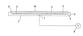
テストウェーハWは、例えば薄くスライスされたφ150mmの半導体ウェーハからなる。また、保持治具1は、薄い剛性の支持基板2に形成される区画空間3と、この区画空間3に一体的に配列される複数の支持突起5と、区画空間3を被覆する可撓性の密着保持層6と、この密着保持層6を変形させる排気孔7とを備え、密着保持層6の表面にテストウェーハWを着脱自在に保持させるよう機能する。
The test wafer W is made of, for example, a thinly sliced φ150 mm semiconductor wafer. The holding jig 1 has a
支持基板2は、図1や図7に示すように、所定の材料を使用してテストウェーハWよりも拡径の平板に形成され、周縁部を除く表面の大部分に平面円形の区画空間3が浅く凹み形成されており、この区画空間3の周縁上部には、密着保持層6の周縁部を支持する平面リング形の段差部4が切り欠かれる。この支持基板2の所定の材料としては、例えばポリカーボネート、アルミニウム合金、ステンレス、マグネシウム合金、ガラス繊維強化エポキシ樹脂等があげられる。
As shown in FIGS. 1 and 7, the support substrate 2 is formed into a flat plate having a diameter larger than that of the test wafer W by using a predetermined material. A flat ring-shaped stepped portion 4 that supports the peripheral portion of the adhesion holding layer 6 is cut out at the upper peripheral edge of the
複数の支持突起5は、例えば電鋳により金属を所定の形に析出する方法、支持基板2の表面を支持突起部分を残して侵食除去するエッチング法、支持基板2の表面を支持突起部分を残して除去するサンドブラスト法、支持基板2にレジスト層を積層して露光後、現像により支持突起5を配設するレジスト法、スクリーン印刷法等により配設される。各支持突起5は、区画空間3の底から上方に指向する円柱形あるいは円錐台形に形成され、表面(上面)が密着保持層6の裏面に接着剤を介して接着されており、区画空間3の段差部4に張架された密着保持層6を水平に支持するよう機能する。
The plurality of
密着保持層6は、図7に示すように、所定の材料を使用して弾性変形可能な薄い円板に形成され、区画空間3の段差部4に接着されて区画空間3と複数の支持突起5とを被覆する。この密着保持層6の所定の材料としては、例えば耐熱性や弾性に優れるフッ素系、シリコーン系のエラストマー、各種の樹脂フィルム等があげられる。この所定の材料には、必要に応じ、補強性フィラーや疎水性シリカ等が選択的に添加される。密着保持層6の製造方法としては、特に限定されるものではないが、例えばカレンダー法、コーティング法、プレス法、印刷法等があげられる。
As shown in FIG. 7, the close contact holding layer 6 is formed into a thin disc that can be elastically deformed using a predetermined material, and is adhered to the stepped portion 4 of the
排気孔7は、図7に示すように、例えば支持基板2の中心部厚さ方向に穿孔されて区画空間3に連通し、外部の真空ポンプ8に着脱自在に接続される。このような排気孔7は、真空ポンプ8の駆動により密着保持層6に密閉被覆された区画空間3の空気を外部に排気して平坦な密着保持層6を複数の支持突起5に応じ断面凹凸に変形させ、密着保持層6とテストウェーハWとの間に空気流入用の隙間を形成して密着状態のテストウェーハWを取り外し可能とする。
As shown in FIG. 7, the
容器本体10と蓋体20とは、所定の樹脂を含む成形材料を使用して真空成形法あるいは圧空成形法等によりそれぞれ安価に成形される。成形材料の所定の樹脂としては、特に限定されるものではないが、例えばナイロン、ポリエチレンテレフタレート、ポリカーボネート等があげられる。
The
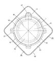
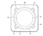
容器本体10は、図1ないし図4に示すように、平板の周囲から周壁12が下方向に伸びる断面略溝形の本体部11を備え、この本体部11に、周壁上端部に保持治具1の周縁部を支持する錐台部13が凹み形成されており、これら本体部11と錐台部13との間には、保持治具1の周縁部を規制する複数のストッパ部18が介在して形成される。容器本体10の本体部11は、平面略矩形に形成され、上下方向に指向する周壁12の端部が水平外方向に短く屈曲形成されて補強機能を発揮する。
As shown in FIGS. 1 to 4, the container
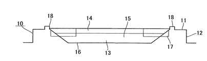
錐台部13は、本体部11の大部分に凹み形成される中空円錐台形の拡径部14と、この拡径部14の下端に連設されて保持治具1の裏面に緩衝用の空隙15を介して対向する断面略すり鉢形の縮径部16とを備えた中空の円錐台形に屈曲形成され、傾斜した拡径部14の内周上端に支持基板2の周縁部を線接触で支持する。
The
容器本体10の本体部11から錐台部13の周壁、換言すれば、本体部11から拡径部14の周壁にかけては、複数のストッパ部18間に位置する複数の被嵌合部17が凹み形成され、各被嵌合部17が平面略舌形に形成される。
A plurality of fitted
複数のストッパ部18は、本体部11の表面と錐台部13の周壁上端部との間に所定の間隔をおいて配列形成され、保持治具1を包囲する。各ストッパ部18は、錐台部13の開口周縁に沿う平面略半円弧形の断面矩形に突出形成され、支持基板2の周縁部に接触して位置決めする。
The plurality of
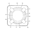
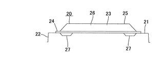
蓋体20は、図1、図2、図5、図6に示すように、容器本体10の本体部11表面に上方から重なる断面略溝形の本体蓋部21を備え、この本体蓋部21には、容器本体10の錐台部13と複数のストッパ部18とを覆う錐台ドーム部23が膨出凹み形成される。蓋体20の本体蓋部21は、平板の周囲から周壁22が下方向に伸びる平面略矩形に形成され、上下方向に指向する周壁22の端部が水平外方向に短く屈曲形成されて補強機能を営む。
As shown in FIGS. 1, 2, 5, and 6, the
錐台ドーム部23は、本体蓋部21の大部分に凹み形成されて容器本体10のストッパ部18を覆う拡径部24と、この拡径部24に連設される断面略すり鉢形の縮径部25とを備えた中空の円錐台形に屈曲形成され、テストウェーハWや保持治具1と縮径部25との間に緩衝用の空隙26を形成するよう機能する。
The
本体蓋部21から錐台ドーム部23、換言すれば、本体蓋部21から錐台ドーム部23の拡径部24にかけては、容器本体10の複数の被嵌合部17にそれぞれ嵌合される中空の嵌合部27が所定の間隔をおいて凹み形成され、この複数の嵌合部27の一部の周面、換言すれば、保持治具1の周縁部に対向する周面が容器本体10の錐台部13方向に向け徐々に傾斜形成される。この保持治具1の周縁部に対向する各嵌合部27の周面は、被嵌合部17内で支持基板2の周縁部を強固に線接触で支持し、錐台部13の拡径部14と共に保持治具1の姿勢を水平に安定させるよう機能する。
From the
上記において、テストウェーハWを保持治具1に保持して搬送容器で搬送する場合には、先ず、密着保持層6の表面にテストウェーハWを重ねて押圧することにより、密着保持層6の表面にテストウェーハWを隙間なく密着し、保持治具1にテストウェーハWを着脱自在に粘着保持させる。 In the above, when the test wafer W is held on the holding jig 1 and transferred by the transfer container, first, the test wafer W is stacked on the surface of the close contact holding layer 6 and pressed, thereby pressing the surface of the close contact holding layer 6. The test wafer W is brought into close contact with the gap, and the test wafer W is detachably adhered to the holding jig 1.
なお、密着保持層6からテストウェーハWを取り外したい場合には、支持基板2の排気孔7に真空ポンプ8を排気管を介して接続し、真空ポンプ8を駆動すれば良い。すると、密着保持層6に密閉被覆された区画空間3の空気が排気孔7と排気管とを順次経由して外部に吸引排気され、平らな密着保持層6が複数の支持突起5に応じ凹凸に変形してテストウェーハWとの間に空気流入用の隙間を複数形成し、この隙間の形成により、粘着されたテストウェーハWを容易に取り外すことが可能となる。
In order to remove the test wafer W from the adhesion holding layer 6, the
保持治具1にテストウェーハWを着脱自在に粘着保持させたら、搬送容器の容器本体10の錐台部13に保持治具1を嵌入支持させるとともに、複数のストッパ部18により保持治具1を位置決めし、その後、容器本体10の表面に蓋体20を被せて容器本体10の各被嵌合部17に蓋体20の嵌合部27を密嵌させ、各嵌合部27の傾いた周面を支持基板2の周縁部に線接触させれば、テストウェーハWを1枚収納して搬送することができる。
When the test wafer W is detachably adhered and held on the holding jig 1, the holding jig 1 is fitted and supported on the
上記によれば、専用の搬送容器にテストウェーハWを1枚収納して保管、出荷、搬送、輸送することができるので、スペースの無駄を省き、収納効率を向上させることができる。また、テストウェーハWを直接搬送容器に収納するのではなく、テストウェーハWを保持した保持治具1を搬送容器に収納するので、搬送時の振動等でテストウェーハWの周縁部等が損傷するおそれがなく、搬送の安全性を著しく向上させることができる。 According to the above, since one test wafer W can be stored, stored, shipped, transported, and transported in a dedicated transport container, waste of space can be saved and storage efficiency can be improved. Further, since the holding jig 1 holding the test wafer W is not stored directly in the transfer container but is stored in the transfer container, the periphery of the test wafer W is damaged due to vibration during transfer. There is no fear, and the safety of conveyance can be remarkably improved.
また、容器本体10の錐台部13に保持治具1を面接触ではなく、線接触で支持させて接触領域を減少させるので、塵埃の発生のおそれを有効に排除することができる。さらに、容器本体10の錐台部13と蓋体20の錐台ドーム部23とが保持治具1との間にそれぞれ空隙15・26を形成するので、これらとテストウェーハWとの接触に伴う汚染を防止することができる他、搬送容器の落下時にテストウェーハWや保持治具1に作用する衝撃を弱化させることができ、テストウェーハWや保持治具1を有効に保護することが可能になる。
Further, since the holding jig 1 is supported not by surface contact but by line contact on the
なお、上記実施形態における保持治具1の排気孔7は、支持基板2の中心部に穿孔しても良いし、中心部から半径外方向にずれた箇所に必要数設けても良い。 In addition, the exhaust holes 7 of the holding jig 1 in the above embodiment may be perforated in the center portion of the support substrate 2 or may be provided in a necessary number at locations shifted radially outward from the center portion.
1 保持治具
2 支持基板
3 区画空間
5 支持突起
6 密着保持層(保持層)
7 排気孔
10 容器本体
11 本体部
13 錐台部
14 拡径部
15 空隙
16 縮径部
17 被嵌合部
18 ストッパ部
20 蓋体
21 本体蓋部
23 錐台ドーム部
26 空隙
27 嵌合部
W テストウェーハ(ウェーハ)
DESCRIPTION OF SYMBOLS 1 Holding jig 2
7
Claims (3)
容器本体は、断面略溝形の本体部と、この本体部に凹み形成されて周壁にウェーハを搭載する保持治具を支持する中空の錐台部と、本体部と錐台部との間に形成されて保持治具を規制するストッパ部とを含み、
蓋体は、容器本体の本体部に重なる断面略溝形の本体蓋部と、この本体蓋部に形成されて容器本体の錐台部とストッパ部とを覆う中空の錐台ドーム部とを含んでなることを特徴とする保持治具の搬送容器。 A holding container carrying container for removably fitting a lid to the surface of a container main body that supports a holding jig for a wafer,
The container main body has a substantially groove-shaped main body, a hollow frustum that is recessed in the main body and supports a holding jig for mounting a wafer on the peripheral wall, and the main body and the frustum. Including a stopper portion that is formed and restricts the holding jig,
The lid includes a substantially lid-shaped main body lid portion that overlaps the main body portion of the container main body, and a hollow frustum dome portion that is formed on the main body lid portion and covers the frustum portion and the stopper portion of the container main body. A holding jig transport container characterized by comprising:
Priority Applications (1)
| Application Number | Priority Date | Filing Date | Title |
|---|---|---|---|
| JP2008203724A JP5147592B2 (en) | 2008-08-07 | 2008-08-07 | Holding jig transport container |
Applications Claiming Priority (1)
| Application Number | Priority Date | Filing Date | Title |
|---|---|---|---|
| JP2008203724A JP5147592B2 (en) | 2008-08-07 | 2008-08-07 | Holding jig transport container |
Publications (2)
| Publication Number | Publication Date |
|---|---|
| JP2010040887A true JP2010040887A (en) | 2010-02-18 |
| JP5147592B2 JP5147592B2 (en) | 2013-02-20 |
Family
ID=42013093
Family Applications (1)
| Application Number | Title | Priority Date | Filing Date |
|---|---|---|---|
| JP2008203724A Expired - Fee Related JP5147592B2 (en) | 2008-08-07 | 2008-08-07 | Holding jig transport container |
Country Status (1)
| Country | Link |
|---|---|
| JP (1) | JP5147592B2 (en) |
Cited By (2)
| Publication number | Priority date | Publication date | Assignee | Title |
|---|---|---|---|---|
| JP2013219096A (en) * | 2012-04-05 | 2013-10-24 | Shin Etsu Polymer Co Ltd | Protective tape for semiconductor wafer and sticking method thereof |
| US9761470B2 (en) | 2014-05-08 | 2017-09-12 | Toyota Jidosha Kabushiki Kaisha | Wafer carrier |
Citations (6)
| Publication number | Priority date | Publication date | Assignee | Title |
|---|---|---|---|---|
| JPH06204328A (en) * | 1992-12-25 | 1994-07-22 | Mitsubishi Materials Corp | Wafer case |
| JPH10142772A (en) * | 1996-11-07 | 1998-05-29 | Shin Etsu Polymer Co Ltd | Pellicle housing vessel |
| JP2003307831A (en) * | 2002-04-16 | 2003-10-31 | Asahi Glass Co Ltd | Synthetic quartz glass container |
| JP2004311779A (en) * | 2003-04-08 | 2004-11-04 | Shin Etsu Polymer Co Ltd | Semiconductor wafer storage container and method for conveying semiconductor wafer |
| JP2005235994A (en) * | 2004-02-19 | 2005-09-02 | Sumitomo Electric Ind Ltd | Wafer tray |
| WO2006087894A1 (en) * | 2005-02-03 | 2006-08-24 | Shin-Etsu Polymer Co., Ltd. | Fixation carrier, production method of fixation carrier, use method of fixation carrier, and substrate reception container |
-
2008
- 2008-08-07 JP JP2008203724A patent/JP5147592B2/en not_active Expired - Fee Related
Patent Citations (6)
| Publication number | Priority date | Publication date | Assignee | Title |
|---|---|---|---|---|
| JPH06204328A (en) * | 1992-12-25 | 1994-07-22 | Mitsubishi Materials Corp | Wafer case |
| JPH10142772A (en) * | 1996-11-07 | 1998-05-29 | Shin Etsu Polymer Co Ltd | Pellicle housing vessel |
| JP2003307831A (en) * | 2002-04-16 | 2003-10-31 | Asahi Glass Co Ltd | Synthetic quartz glass container |
| JP2004311779A (en) * | 2003-04-08 | 2004-11-04 | Shin Etsu Polymer Co Ltd | Semiconductor wafer storage container and method for conveying semiconductor wafer |
| JP2005235994A (en) * | 2004-02-19 | 2005-09-02 | Sumitomo Electric Ind Ltd | Wafer tray |
| WO2006087894A1 (en) * | 2005-02-03 | 2006-08-24 | Shin-Etsu Polymer Co., Ltd. | Fixation carrier, production method of fixation carrier, use method of fixation carrier, and substrate reception container |
Cited By (2)
| Publication number | Priority date | Publication date | Assignee | Title |
|---|---|---|---|---|
| JP2013219096A (en) * | 2012-04-05 | 2013-10-24 | Shin Etsu Polymer Co Ltd | Protective tape for semiconductor wafer and sticking method thereof |
| US9761470B2 (en) | 2014-05-08 | 2017-09-12 | Toyota Jidosha Kabushiki Kaisha | Wafer carrier |
Also Published As
| Publication number | Publication date |
|---|---|
| JP5147592B2 (en) | 2013-02-20 |
Similar Documents
| Publication | Publication Date | Title |
|---|---|---|
| JP5074125B2 (en) | Fixing jig and workpiece processing method | |
| CN107665844B (en) | Wafer cassette, method of arranging wafers in wafer cassette, wafer protection plate, and method of protecting wafers | |
| JP2008103494A (en) | Fixing jig and chip pickup method and pickup device | |
| JP2005327758A (en) | Part holder | |
| JP4797027B2 (en) | Substrate body sticking apparatus and substrate body handling method | |
| JP5147592B2 (en) | Holding jig transport container | |
| JP5995636B2 (en) | Support jig for semiconductor wafer plating | |
| JP2010205817A (en) | Electronic component holder | |
| JP4484760B2 (en) | Fixed carrier and manufacturing method thereof | |
| JP2007157847A (en) | Chucking device | |
| JP4987577B2 (en) | Fixing jig for goods | |
| JP4897312B2 (en) | Fixed carrier | |
| JP4587828B2 (en) | Fixing jig for precision substrates | |
| JP5318557B2 (en) | Holding jig | |
| JP5995628B2 (en) | Support jig for semiconductor wafer plating | |
| JP4450766B2 (en) | Manufacturing method of reinforced carrier | |
| JP4693488B2 (en) | Fixed carrier | |
| JP4834010B2 (en) | Handling method of semiconductor wafer | |
| JP4688567B2 (en) | Fixed carrier | |
| JP2009054628A (en) | Substrate holder | |
| JP5191305B2 (en) | Wafer transport container | |
| JP2012164748A (en) | Wafer protection jig and wafer handling method | |
| JP2007168025A (en) | Holding table, processing device of held article and processing device of semiconductor wafer | |
| JP6017909B2 (en) | Support jig for semiconductor wafer plating | |
| JP2010036974A (en) | Holding jig |
Legal Events
| Date | Code | Title | Description |
|---|---|---|---|
| A621 | Written request for application examination |
Free format text: JAPANESE INTERMEDIATE CODE: A621 Effective date: 20110803 |
|
| A977 | Report on retrieval |
Free format text: JAPANESE INTERMEDIATE CODE: A971007 Effective date: 20120712 |
|
| A131 | Notification of reasons for refusal |
Free format text: JAPANESE INTERMEDIATE CODE: A131 Effective date: 20120717 |
|
| A521 | Request for written amendment filed |
Free format text: JAPANESE INTERMEDIATE CODE: A523 Effective date: 20120910 |
|
| TRDD | Decision of grant or rejection written | ||
| A01 | Written decision to grant a patent or to grant a registration (utility model) |
Free format text: JAPANESE INTERMEDIATE CODE: A01 Effective date: 20121127 |
|
| A61 | First payment of annual fees (during grant procedure) |
Free format text: JAPANESE INTERMEDIATE CODE: A61 Effective date: 20121127 |
|
| R150 | Certificate of patent or registration of utility model |
Ref document number: 5147592 Country of ref document: JP Free format text: JAPANESE INTERMEDIATE CODE: R150 Free format text: JAPANESE INTERMEDIATE CODE: R150 |
|
| FPAY | Renewal fee payment (event date is renewal date of database) |
Free format text: PAYMENT UNTIL: 20151207 Year of fee payment: 3 |
|
| R250 | Receipt of annual fees |
Free format text: JAPANESE INTERMEDIATE CODE: R250 |
|
| R250 | Receipt of annual fees |
Free format text: JAPANESE INTERMEDIATE CODE: R250 |
|
| LAPS | Cancellation because of no payment of annual fees |