JP2010034432A - 半導体装置とその製造方法 - Google Patents
半導体装置とその製造方法 Download PDFInfo
- Publication number
- JP2010034432A JP2010034432A JP2008197206A JP2008197206A JP2010034432A JP 2010034432 A JP2010034432 A JP 2010034432A JP 2008197206 A JP2008197206 A JP 2008197206A JP 2008197206 A JP2008197206 A JP 2008197206A JP 2010034432 A JP2010034432 A JP 2010034432A
- Authority
- JP
- Japan
- Prior art keywords
- opening
- hole
- insulating layer
- semiconductor substrate
- layer
- Prior art date
- Legal status (The legal status is an assumption and is not a legal conclusion. Google has not performed a legal analysis and makes no representation as to the accuracy of the status listed.)
- Granted
Links
Images


Classifications
-
- H10W20/023—
-
- H10W20/0234—
-
- H10W20/0242—
-
- H10W20/20—
-
- H10W20/2125—
-
- H10W70/05—
-
- H10W70/65—
-
- H10W72/20—
-
- H10W72/242—
-
- H10W72/244—
-
- H10W72/29—
-
- H10W72/90—
-
- H10W72/922—
-
- H10W72/923—
-
- H10W72/944—
-
- H10W72/952—
-
- H10W72/953—
Landscapes
- Internal Circuitry In Semiconductor Integrated Circuit Devices (AREA)
Abstract
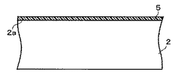
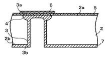
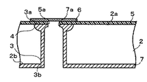
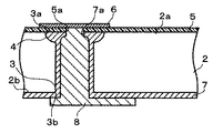
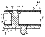
【解決手段】半導体装置1は貫通孔3を有する半導体基板2を備える。貫通孔3は半導体基板2の第1の面2aに開口された第1の開口3aの開口径が第2の面2bに開口された第2の開口3bに近い側の内径より大きくなるように、第1の面2aの近傍を拡張させる拡張部4を備える。半導体基板2の第1の面2aには第1の絶縁層5と第1の配線層6とが設けられている。貫通孔3には拡張部4を充填しつつ内壁面を覆う第2の絶縁層7が設けられており、さらに第1および第2の絶縁層5、7の開口を介して第1の配線層6と接続された第2の配線層8が設けられている。
【選択図】図1
Description
Claims (5)
- 第1の面と、前記第1の面とは反対側の第2の面とを有する半導体基板と、
前記半導体基板に設けられ、前記第1の面に開口された第1の開口と前記第2の面に開口された第2の開口とを有する貫通孔であって、前記第1の開口の開口径が前記第2の開口に近い側の内径より大きくなるように前記第1の面の近傍を拡張させる拡張部を備える貫通孔と、
前記半導体基板の前記第1の面に設けられ、前記貫通孔に連通されていると共に、前記第1の開口の開口径より小径の開口を有する第1の絶縁層と、
前記第1の絶縁層の前記開口を塞ぐように、前記第1の絶縁層上に設けられた第1の配線層と、
前記貫通孔の前記拡張部を充填すると共に、前記貫通孔の前記第1の開口、前記貫通孔の内壁面、および前記半導体基板の前記第2の面を覆うように設けられ、前記第1の絶縁層の前記開口から連通して前記第1の配線層を露出させる開口を有する第2の絶縁層と、
前記第1および第2の絶縁層の前記開口を介して前記第1の配線層と接続するように、前記貫通孔内から前記半導体基板の前記第2の面に亘って、前記第2の絶縁層を介して設けられた第2の配線層と
を具備することを特徴とする半導体装置。 - 請求項1記載の半導体装置において、
前記拡張部は、前記第1の開口の開口端から前記第2の絶縁層の前記開口の開口端までの距離が3〜10μmの範囲で、かつ前記第1の開口から前記第2の開口に近い側の内径部分までの距離が1〜5μmの範囲の形状を有することを特徴とする半導体装置。 - 請求項1記載の半導体装置において、
前記拡張部には有機絶縁物からなる前記第2の絶縁層が充填されていることを特徴とする半導体装置。 - 請求項1記載の半導体装置において、
前記第2の絶縁層は下地膜と絶縁膜との二層構造膜を有し、前記拡張部には前記絶縁膜が充填されていることを特徴とする半導体装置。 - 半導体基板の第1の面に第1の絶縁層を形成する工程と、
前記第1の絶縁層上に第1の配線層を形成する工程と、
前記第1の絶縁層を露出させるように、前記半導体基板の前記第1の面とは反対側の第2の面から前記第1の面に向けて、前記半導体基板に貫通孔を形成しつつ、前記貫通孔に前記第1の面に開口された第1の開口の開口径が前記第2の面に開口された第2の開口に近い側の内径より大きくなるように前記第1の面の近傍を拡張させる拡張部を設ける工程と、
前記貫通孔の前記拡張部を充填しつつ、前記貫通孔の前記第1の開口、前記貫通孔の内壁面、および前記半導体基板の前記第2の面を覆う第2の絶縁層を形成する工程と、
前記貫通孔の底部に存在する前記第1および第2の絶縁層に開口を形成し、前記貫通孔内に前記第1の配線層を露出させる工程と、
前記貫通孔内から前記半導体基板の前記第2の面に亘って、前記第1および第2の絶縁層の前記開口を介して前記第1の配線層と接続する第2の配線層を、前記第2の絶縁層を介して形成する工程と
を具備することを特徴とする半導体装置の製造方法。
Priority Applications (2)
| Application Number | Priority Date | Filing Date | Title |
|---|---|---|---|
| JP2008197206A JP5242282B2 (ja) | 2008-07-31 | 2008-07-31 | 半導体装置とその製造方法 |
| US12/533,492 US8237285B2 (en) | 2008-07-31 | 2009-07-31 | Semiconductor device, through hole having expansion portion and thin insulating film |
Applications Claiming Priority (1)
| Application Number | Priority Date | Filing Date | Title |
|---|---|---|---|
| JP2008197206A JP5242282B2 (ja) | 2008-07-31 | 2008-07-31 | 半導体装置とその製造方法 |
Publications (2)
| Publication Number | Publication Date |
|---|---|
| JP2010034432A true JP2010034432A (ja) | 2010-02-12 |
| JP5242282B2 JP5242282B2 (ja) | 2013-07-24 |
Family
ID=41607494
Family Applications (1)
| Application Number | Title | Priority Date | Filing Date |
|---|---|---|---|
| JP2008197206A Expired - Fee Related JP5242282B2 (ja) | 2008-07-31 | 2008-07-31 | 半導体装置とその製造方法 |
Country Status (2)
| Country | Link |
|---|---|
| US (1) | US8237285B2 (ja) |
| JP (1) | JP5242282B2 (ja) |
Cited By (1)
| Publication number | Priority date | Publication date | Assignee | Title |
|---|---|---|---|---|
| KR101195461B1 (ko) | 2010-09-01 | 2012-10-30 | 에스케이하이닉스 주식회사 | 반도체칩 및 이의 제조방법 |
Families Citing this family (6)
| Publication number | Priority date | Publication date | Assignee | Title |
|---|---|---|---|---|
| JP2011238742A (ja) * | 2010-05-10 | 2011-11-24 | Shinko Electric Ind Co Ltd | 配線基板の製造方法及び配線基板 |
| KR20120031811A (ko) * | 2010-09-27 | 2012-04-04 | 삼성전자주식회사 | 반도체 장치 및 그 제조 방법 |
| US9190325B2 (en) * | 2010-09-30 | 2015-11-17 | Taiwan Semiconductor Manufacturing Company, Ltd. | TSV formation |
| US8742477B1 (en) * | 2010-12-06 | 2014-06-03 | Xilinx, Inc. | Elliptical through silicon vias for active interposers |
| US8816505B2 (en) * | 2011-07-29 | 2014-08-26 | Tessera, Inc. | Low stress vias |
| CA2888605A1 (en) * | 2012-10-17 | 2014-04-24 | Nestec S.A. | Wearable package for consumable products and methods for using same |
Citations (3)
| Publication number | Priority date | Publication date | Assignee | Title |
|---|---|---|---|---|
| JP2006165112A (ja) * | 2004-12-03 | 2006-06-22 | Sharp Corp | 貫通電極形成方法およびそれを用いる半導体装置の製造方法、ならびに該方法によって得られる半導体装置 |
| JP2006287206A (ja) * | 2005-03-10 | 2006-10-19 | Sanyo Electric Co Ltd | 半導体装置及びその製造方法 |
| JP2007305960A (ja) * | 2006-04-14 | 2007-11-22 | Sharp Corp | 半導体装置およびその製造方法 |
Family Cites Families (8)
| Publication number | Priority date | Publication date | Assignee | Title |
|---|---|---|---|---|
| JP3724110B2 (ja) * | 1997-04-24 | 2005-12-07 | 三菱電機株式会社 | 半導体装置の製造方法 |
| JP3457277B2 (ja) * | 1999-12-15 | 2003-10-14 | 沖電気工業株式会社 | 半導体装置および半導体装置の製造方法 |
| JP4703061B2 (ja) | 2001-08-30 | 2011-06-15 | 富士通株式会社 | 薄膜回路基板の製造方法およびビア形成基板の形成方法 |
| JP4289146B2 (ja) * | 2003-03-27 | 2009-07-01 | セイコーエプソン株式会社 | 三次元実装型半導体装置の製造方法 |
| US7180149B2 (en) | 2003-08-28 | 2007-02-20 | Fujikura Ltd. | Semiconductor package with through-hole |
| JP4443379B2 (ja) | 2004-10-26 | 2010-03-31 | 三洋電機株式会社 | 半導体装置の製造方法 |
| US7262134B2 (en) * | 2005-09-01 | 2007-08-28 | Micron Technology, Inc. | Microfeature workpieces and methods for forming interconnects in microfeature workpieces |
| US7855438B2 (en) * | 2006-09-19 | 2010-12-21 | Infineon Technologies Ag | Deep via construction for a semiconductor device |
-
2008
- 2008-07-31 JP JP2008197206A patent/JP5242282B2/ja not_active Expired - Fee Related
-
2009
- 2009-07-31 US US12/533,492 patent/US8237285B2/en not_active Expired - Fee Related
Patent Citations (3)
| Publication number | Priority date | Publication date | Assignee | Title |
|---|---|---|---|---|
| JP2006165112A (ja) * | 2004-12-03 | 2006-06-22 | Sharp Corp | 貫通電極形成方法およびそれを用いる半導体装置の製造方法、ならびに該方法によって得られる半導体装置 |
| JP2006287206A (ja) * | 2005-03-10 | 2006-10-19 | Sanyo Electric Co Ltd | 半導体装置及びその製造方法 |
| JP2007305960A (ja) * | 2006-04-14 | 2007-11-22 | Sharp Corp | 半導体装置およびその製造方法 |
Cited By (1)
| Publication number | Priority date | Publication date | Assignee | Title |
|---|---|---|---|---|
| KR101195461B1 (ko) | 2010-09-01 | 2012-10-30 | 에스케이하이닉스 주식회사 | 반도체칩 및 이의 제조방법 |
Also Published As
| Publication number | Publication date |
|---|---|
| JP5242282B2 (ja) | 2013-07-24 |
| US8237285B2 (en) | 2012-08-07 |
| US20100025860A1 (en) | 2010-02-04 |
Similar Documents
| Publication | Publication Date | Title |
|---|---|---|
| US8232202B2 (en) | Image sensor package and fabrication method thereof | |
| CN101483162B (zh) | 半导体装置及其制造方法 | |
| JP5242282B2 (ja) | 半導体装置とその製造方法 | |
| US8390125B2 (en) | Through-silicon via formed with a post passivation interconnect structure | |
| CN102456650B (zh) | 半导体基板的导电结构以及其制造方法 | |
| TWI311790B (en) | Semiconductor device having bonding pad above low-k kielectric film and manufacturing method therefor | |
| JP2011009645A (ja) | 半導体装置及びその製造方法 | |
| JP2008305938A (ja) | 半導体装置および半導体装置の製造方法 | |
| US7880256B2 (en) | Semiconductor device with passivation layer covering wiring layer | |
| JP2004327910A (ja) | 半導体装置およびその製造方法 | |
| JP2011096918A (ja) | 半導体装置および半導体装置の製造方法 | |
| US20200350284A1 (en) | Semiconductor device and method of manufacturing the same | |
| US20100096749A1 (en) | Semiconductor package and manufacturing method thereof | |
| JP5245135B2 (ja) | 貫通導電体を有する半導体装置およびその製造方法 | |
| TW201216429A (en) | Conductive pillar structure | |
| TWI298517B (en) | Manufacturing method for electronic component, electronic component, and electronic equipment | |
| JP2005235860A (ja) | 半導体装置及びその製造方法 | |
| US8129835B2 (en) | Package substrate having semiconductor component embedded therein and fabrication method thereof | |
| CN100524725C (zh) | 半导体装置及其制造方法 | |
| JP2008300718A (ja) | 半導体装置および半導体装置の製造方法 | |
| JP2010232400A (ja) | 半導体基板と半導体基板の製造方法および半導体パッケージ | |
| JP2011223234A (ja) | 圧電振動子、圧電デバイス、貫通電極構造、半導体装置、半導体パッケージ | |
| JP2009212271A (ja) | 半導体装置およびその製造方法 | |
| TWI437689B (zh) | 半導體裝置 | |
| JP2009088002A (ja) | 半導体装置及びその製造方法 |
Legal Events
| Date | Code | Title | Description |
|---|---|---|---|
| A621 | Written request for application examination |
Free format text: JAPANESE INTERMEDIATE CODE: A621 Effective date: 20100913 |
|
| RD02 | Notification of acceptance of power of attorney |
Free format text: JAPANESE INTERMEDIATE CODE: A7422 Effective date: 20120614 |
|
| A977 | Report on retrieval |
Free format text: JAPANESE INTERMEDIATE CODE: A971007 Effective date: 20121219 |
|
| A131 | Notification of reasons for refusal |
Free format text: JAPANESE INTERMEDIATE CODE: A131 Effective date: 20121225 |
|
| A521 | Request for written amendment filed |
Free format text: JAPANESE INTERMEDIATE CODE: A523 Effective date: 20130225 |
|
| TRDD | Decision of grant or rejection written | ||
| A01 | Written decision to grant a patent or to grant a registration (utility model) |
Free format text: JAPANESE INTERMEDIATE CODE: A01 Effective date: 20130312 |
|
| A61 | First payment of annual fees (during grant procedure) |
Free format text: JAPANESE INTERMEDIATE CODE: A61 Effective date: 20130403 |
|
| FPAY | Renewal fee payment (event date is renewal date of database) |
Free format text: PAYMENT UNTIL: 20160412 Year of fee payment: 3 |
|
| R151 | Written notification of patent or utility model registration |
Ref document number: 5242282 Country of ref document: JP Free format text: JAPANESE INTERMEDIATE CODE: R151 |
|
| FPAY | Renewal fee payment (event date is renewal date of database) |
Free format text: PAYMENT UNTIL: 20160412 Year of fee payment: 3 |
|
| S111 | Request for change of ownership or part of ownership |
Free format text: JAPANESE INTERMEDIATE CODE: R313111 |
|
| R350 | Written notification of registration of transfer |
Free format text: JAPANESE INTERMEDIATE CODE: R350 |
|
| LAPS | Cancellation because of no payment of annual fees |