JP2010034347A - 回路装置 - Google Patents
回路装置 Download PDFInfo
- Publication number
- JP2010034347A JP2010034347A JP2008195783A JP2008195783A JP2010034347A JP 2010034347 A JP2010034347 A JP 2010034347A JP 2008195783 A JP2008195783 A JP 2008195783A JP 2008195783 A JP2008195783 A JP 2008195783A JP 2010034347 A JP2010034347 A JP 2010034347A
- Authority
- JP
- Japan
- Prior art keywords
- conductive pattern
- power element
- power
- circuit
- conductive
- Prior art date
- Legal status (The legal status is an assumption and is not a legal conclusion. Google has not performed a legal analysis and makes no representation as to the accuracy of the status listed.)
- Granted
Links
Images

Classifications
-
- H—ELECTRICITY
- H01—ELECTRIC ELEMENTS
- H01L—SEMICONDUCTOR DEVICES NOT COVERED BY CLASS H10
- H01L2224/00—Indexing scheme for arrangements for connecting or disconnecting semiconductor or solid-state bodies and methods related thereto as covered by H01L24/00
- H01L2224/01—Means for bonding being attached to, or being formed on, the surface to be connected, e.g. chip-to-package, die-attach, "first-level" interconnects; Manufacturing methods related thereto
- H01L2224/42—Wire connectors; Manufacturing methods related thereto
- H01L2224/47—Structure, shape, material or disposition of the wire connectors after the connecting process
- H01L2224/48—Structure, shape, material or disposition of the wire connectors after the connecting process of an individual wire connector
- H01L2224/4805—Shape
- H01L2224/4809—Loop shape
- H01L2224/48091—Arched
-
- H—ELECTRICITY
- H01—ELECTRIC ELEMENTS
- H01L—SEMICONDUCTOR DEVICES NOT COVERED BY CLASS H10
- H01L2224/00—Indexing scheme for arrangements for connecting or disconnecting semiconductor or solid-state bodies and methods related thereto as covered by H01L24/00
- H01L2224/01—Means for bonding being attached to, or being formed on, the surface to be connected, e.g. chip-to-package, die-attach, "first-level" interconnects; Manufacturing methods related thereto
- H01L2224/42—Wire connectors; Manufacturing methods related thereto
- H01L2224/47—Structure, shape, material or disposition of the wire connectors after the connecting process
- H01L2224/49—Structure, shape, material or disposition of the wire connectors after the connecting process of a plurality of wire connectors
- H01L2224/491—Disposition
- H01L2224/4911—Disposition the connectors being bonded to at least one common bonding area, e.g. daisy chain
- H01L2224/49111—Disposition the connectors being bonded to at least one common bonding area, e.g. daisy chain the connectors connecting two common bonding areas, e.g. Litz or braid wires
-
- H—ELECTRICITY
- H01—ELECTRIC ELEMENTS
- H01L—SEMICONDUCTOR DEVICES NOT COVERED BY CLASS H10
- H01L2224/00—Indexing scheme for arrangements for connecting or disconnecting semiconductor or solid-state bodies and methods related thereto as covered by H01L24/00
- H01L2224/73—Means for bonding being of different types provided for in two or more of groups H01L2224/10, H01L2224/18, H01L2224/26, H01L2224/34, H01L2224/42, H01L2224/50, H01L2224/63, H01L2224/71
- H01L2224/732—Location after the connecting process
- H01L2224/73251—Location after the connecting process on different surfaces
- H01L2224/73265—Layer and wire connectors
-
- H—ELECTRICITY
- H01—ELECTRIC ELEMENTS
- H01L—SEMICONDUCTOR DEVICES NOT COVERED BY CLASS H10
- H01L2924/00—Indexing scheme for arrangements or methods for connecting or disconnecting semiconductor or solid-state bodies as covered by H01L24/00
- H01L2924/10—Details of semiconductor or other solid state devices to be connected
- H01L2924/11—Device type
- H01L2924/13—Discrete devices, e.g. 3 terminal devices
- H01L2924/1304—Transistor
- H01L2924/1305—Bipolar Junction Transistor [BJT]
- H01L2924/13055—Insulated gate bipolar transistor [IGBT]
-
- H—ELECTRICITY
- H01—ELECTRIC ELEMENTS
- H01L—SEMICONDUCTOR DEVICES NOT COVERED BY CLASS H10
- H01L2924/00—Indexing scheme for arrangements or methods for connecting or disconnecting semiconductor or solid-state bodies as covered by H01L24/00
- H01L2924/10—Details of semiconductor or other solid state devices to be connected
- H01L2924/11—Device type
- H01L2924/13—Discrete devices, e.g. 3 terminal devices
- H01L2924/1304—Transistor
- H01L2924/1306—Field-effect transistor [FET]
- H01L2924/13091—Metal-Oxide-Semiconductor Field-Effect Transistor [MOSFET]
-
- H—ELECTRICITY
- H01—ELECTRIC ELEMENTS
- H01L—SEMICONDUCTOR DEVICES NOT COVERED BY CLASS H10
- H01L2924/00—Indexing scheme for arrangements or methods for connecting or disconnecting semiconductor or solid-state bodies as covered by H01L24/00
- H01L2924/19—Details of hybrid assemblies other than the semiconductor or other solid state devices to be connected
- H01L2924/191—Disposition
- H01L2924/19101—Disposition of discrete passive components
- H01L2924/19105—Disposition of discrete passive components in a side-by-side arrangement on a common die mounting substrate
Landscapes
- Inverter Devices (AREA)
Abstract
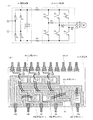
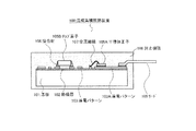
【解決手段】本発明の混成集積回路装置10は、導電パターン26および第1パワー素子18から成る混成集積回路が上面に組み込まれた回路基板12と、回路基板12を被覆して混成集積回路を封止する封止樹脂30と、導電パターン26から成るパッドに固着されて外部に延在するリード14とを有する構成となっている。そして、第1パワー素子18と接続される経路の途中には、厚い導電プレート16が配置されている。
【選択図】図1
Description
12 回路基板
14,14A,14B、14C、14D、14E、14F、14G リード
16 導電プレート
18 第1パワー素子
20 第2パワー素子
22 制御素子
24 チップ素子
26、26A、26B、26C、26D、26E、26F、26G 導電パターン
28 絶縁層
30 封止樹脂
32 接合材
34 整流回路
36 インバータ回路
Claims (6)
- 回路基板と、
前記回路基板の上面に形成された導電パターンと、
前記導電パターンと電気的に接続されたパワー素子と、
前記導電パターンを経由して前記パワー素子と接続されて入出力端子として機能するリードと、を備え、
前記パワー素子と接続される経路の一部分は、前記導電パターンよりも厚い導電プレートから構成されることを特徴とする回路装置。 - 前記リードは、前記回路基板の一側辺に沿って複数個が配置され、
前記パワー素子には、第1パワー素子と、前記第1パワー素子よりも前記リードに接近して配置された第2パワー素子とが含まれ、
前記第1パワー素子は、前記導電プレートおよび前記導電パターンを経由して前記リードと接続され、
前記第2パワー素子は、前記導電プレートを経由せずに前記導電パターンを経由して前記リードと接続されることを特徴とする請求項1記載の回路装置。 - 前記第1パワー素子と前記リードとを接続する経路に於いて、前記導電プレートが配置される領域では、前記導電パターンは分断されることを特徴とする請求項2記載の回路装置。
- 前記回路基板には、前記パワー素子を含むインバータ回路が組み込まれ、
前記パワー素子には、前記インバータ回路のハイサイド側の3つのトランジスタと、ローサイド側の3つのトランジスタとが含まれ、
前記第1パワー素子は、前記インバータ回路を構成する前記トランジスタのいずれかであることを特徴とする請求項3に記載の回路装置。 - 前記導電プレートの断面形状は四角形形状であることを特徴とする請求項4記載の回路装置。
- 前記導電プレートの断面形状は、異形形状であることを特徴とする請求項4記載の回路装置。
Priority Applications (1)
| Application Number | Priority Date | Filing Date | Title |
|---|---|---|---|
| JP2008195783A JP5285348B2 (ja) | 2008-07-30 | 2008-07-30 | 回路装置 |
Applications Claiming Priority (1)
| Application Number | Priority Date | Filing Date | Title |
|---|---|---|---|
| JP2008195783A JP5285348B2 (ja) | 2008-07-30 | 2008-07-30 | 回路装置 |
Publications (2)
| Publication Number | Publication Date |
|---|---|
| JP2010034347A true JP2010034347A (ja) | 2010-02-12 |
| JP5285348B2 JP5285348B2 (ja) | 2013-09-11 |
Family
ID=41738473
Family Applications (1)
| Application Number | Title | Priority Date | Filing Date |
|---|---|---|---|
| JP2008195783A Active JP5285348B2 (ja) | 2008-07-30 | 2008-07-30 | 回路装置 |
Country Status (1)
| Country | Link |
|---|---|
| JP (1) | JP5285348B2 (ja) |
Cited By (9)
| Publication number | Priority date | Publication date | Assignee | Title |
|---|---|---|---|---|
| CN102738134A (zh) * | 2011-04-13 | 2012-10-17 | 三菱电机株式会社 | 半导体装置 |
| JP2013201325A (ja) * | 2012-03-26 | 2013-10-03 | Semiconductor Components Industries Llc | 回路装置 |
| WO2013179547A1 (ja) * | 2012-06-01 | 2013-12-05 | パナソニック株式会社 | パワー半導体装置 |
| WO2014169887A1 (de) * | 2013-04-18 | 2014-10-23 | Forschungszentrum Jülich GmbH | Hochfrequenzleiter mit verbesserter leitfähigkeit |
| JP2016027677A (ja) * | 2012-05-29 | 2016-02-18 | 日本精工株式会社 | 半導体モジュール |
| JP2017152722A (ja) * | 2012-05-15 | 2017-08-31 | ローム株式会社 | パワーモジュール半導体装置 |
| CN107683525A (zh) * | 2016-03-11 | 2018-02-09 | 新电元工业株式会社 | 半导体装置以及引线框 |
| US10943877B2 (en) | 2018-04-11 | 2021-03-09 | Denso Corporation | Semiconductor device |
| US11107761B2 (en) * | 2018-02-06 | 2021-08-31 | Denso Corporation | Semiconductor device |
Citations (5)
| Publication number | Priority date | Publication date | Assignee | Title |
|---|---|---|---|---|
| JPH03174746A (ja) * | 1990-03-29 | 1991-07-29 | Sanyo Electric Co Ltd | 混成集積回路装置 |
| JP2004221460A (ja) * | 2003-01-17 | 2004-08-05 | Matsushita Electric Ind Co Ltd | 半導体部品、半導体装置、及び該半導体装置の製造方法 |
| JP2005174955A (ja) * | 2003-12-05 | 2005-06-30 | Toyota Industries Corp | 半導体モジュール |
| JP2007096212A (ja) * | 2005-09-30 | 2007-04-12 | Fujitsu Ltd | 電気部品の電源ピンへの給電装置 |
| JP2008135735A (ja) * | 2006-10-31 | 2008-06-12 | Sanyo Electric Co Ltd | 回路装置 |
-
2008
- 2008-07-30 JP JP2008195783A patent/JP5285348B2/ja active Active
Patent Citations (5)
| Publication number | Priority date | Publication date | Assignee | Title |
|---|---|---|---|---|
| JPH03174746A (ja) * | 1990-03-29 | 1991-07-29 | Sanyo Electric Co Ltd | 混成集積回路装置 |
| JP2004221460A (ja) * | 2003-01-17 | 2004-08-05 | Matsushita Electric Ind Co Ltd | 半導体部品、半導体装置、及び該半導体装置の製造方法 |
| JP2005174955A (ja) * | 2003-12-05 | 2005-06-30 | Toyota Industries Corp | 半導体モジュール |
| JP2007096212A (ja) * | 2005-09-30 | 2007-04-12 | Fujitsu Ltd | 電気部品の電源ピンへの給電装置 |
| JP2008135735A (ja) * | 2006-10-31 | 2008-06-12 | Sanyo Electric Co Ltd | 回路装置 |
Cited By (15)
| Publication number | Priority date | Publication date | Assignee | Title |
|---|---|---|---|---|
| CN102738134A (zh) * | 2011-04-13 | 2012-10-17 | 三菱电机株式会社 | 半导体装置 |
| JP2012222297A (ja) * | 2011-04-13 | 2012-11-12 | Mitsubishi Electric Corp | 半導体装置 |
| JP2013201325A (ja) * | 2012-03-26 | 2013-10-03 | Semiconductor Components Industries Llc | 回路装置 |
| JP2017152722A (ja) * | 2012-05-15 | 2017-08-31 | ローム株式会社 | パワーモジュール半導体装置 |
| JP2016027677A (ja) * | 2012-05-29 | 2016-02-18 | 日本精工株式会社 | 半導体モジュール |
| JPWO2013179547A1 (ja) * | 2012-06-01 | 2016-01-18 | パナソニックIpマネジメント株式会社 | パワー半導体装置 |
| CN104380462A (zh) * | 2012-06-01 | 2015-02-25 | 松下知识产权经营株式会社 | 功率半导体装置 |
| US9325257B2 (en) | 2012-06-01 | 2016-04-26 | Panasonic Intellectual Property Management Co., Ltd. | Power semiconductor device to reduce voltage variation between terminals |
| WO2013179547A1 (ja) * | 2012-06-01 | 2013-12-05 | パナソニック株式会社 | パワー半導体装置 |
| WO2014169887A1 (de) * | 2013-04-18 | 2014-10-23 | Forschungszentrum Jülich GmbH | Hochfrequenzleiter mit verbesserter leitfähigkeit |
| US9735247B2 (en) | 2013-04-18 | 2017-08-15 | Forschungszentrum Juelich Gmbh | High-frequency conductor having improved conductivity |
| CN107683525A (zh) * | 2016-03-11 | 2018-02-09 | 新电元工业株式会社 | 半导体装置以及引线框 |
| CN107683525B (zh) * | 2016-03-11 | 2020-08-14 | 新电元工业株式会社 | 半导体装置以及引线框 |
| US11107761B2 (en) * | 2018-02-06 | 2021-08-31 | Denso Corporation | Semiconductor device |
| US10943877B2 (en) | 2018-04-11 | 2021-03-09 | Denso Corporation | Semiconductor device |
Also Published As
| Publication number | Publication date |
|---|---|
| JP5285348B2 (ja) | 2013-09-11 |
Similar Documents
| Publication | Publication Date | Title |
|---|---|---|
| JP5285348B2 (ja) | 回路装置 | |
| JP6188902B2 (ja) | 電力用半導体モジュール及び電力変換装置 | |
| JP3674333B2 (ja) | パワー半導体モジュール並びにそれを用いた電動機駆動システム | |
| US9905541B2 (en) | Semiconductor module with bus bar including stacked wiring layers | |
| JP5798412B2 (ja) | 半導体モジュール | |
| JP5434986B2 (ja) | 半導体モジュールおよびそれを備えた半導体装置 | |
| JP4660214B2 (ja) | 電力用半導体装置 | |
| JP5550225B2 (ja) | 回路装置 | |
| US10468338B2 (en) | Semiconductor device | |
| US9468087B1 (en) | Power module with improved cooling and method for making | |
| CN107731779B (zh) | 电子装置 | |
| JP2019506753A (ja) | 多層回路基板に基づくパワーモジュール | |
| JP5285224B2 (ja) | 回路装置 | |
| JP5481104B2 (ja) | 半導体装置 | |
| JP4349364B2 (ja) | 半導体装置 | |
| WO2020262212A1 (ja) | 半導体装置 | |
| US11955407B2 (en) | Electronic module including a semiconductor package connected to a fluid heatsink | |
| JP5147344B2 (ja) | 回路装置およびその製造方法 | |
| JP7035920B2 (ja) | 半導体装置および電力変換装置 | |
| JP2021158232A (ja) | 半導体モジュール | |
| JP2010225952A (ja) | 半導体モジュール | |
| US11145629B2 (en) | Semiconductor device and power conversion device | |
| JP6709313B1 (ja) | 半導体装置および半導体装置の製造方法 | |
| JP5039388B2 (ja) | 回路装置 | |
| JP2024018064A (ja) | 半導体装置 |
Legal Events
| Date | Code | Title | Description |
|---|---|---|---|
| A711 | Notification of change in applicant |
Free format text: JAPANESE INTERMEDIATE CODE: A711 Effective date: 20110602 |
|
| A621 | Written request for application examination |
Free format text: JAPANESE INTERMEDIATE CODE: A621 Effective date: 20110620 |
|
| A977 | Report on retrieval |
Free format text: JAPANESE INTERMEDIATE CODE: A971007 Effective date: 20120907 |
|
| A131 | Notification of reasons for refusal |
Free format text: JAPANESE INTERMEDIATE CODE: A131 Effective date: 20120918 |
|
| A521 | Request for written amendment filed |
Free format text: JAPANESE INTERMEDIATE CODE: A523 Effective date: 20121212 |
|
| A131 | Notification of reasons for refusal |
Free format text: JAPANESE INTERMEDIATE CODE: A131 Effective date: 20130108 |
|
| A711 | Notification of change in applicant |
Free format text: JAPANESE INTERMEDIATE CODE: A711 Effective date: 20130215 |
|
| A521 | Request for written amendment filed |
Free format text: JAPANESE INTERMEDIATE CODE: A523 Effective date: 20130405 |
|
| A521 | Request for written amendment filed |
Free format text: JAPANESE INTERMEDIATE CODE: A523 Effective date: 20130408 |
|
| TRDD | Decision of grant or rejection written | ||
| A01 | Written decision to grant a patent or to grant a registration (utility model) |
Free format text: JAPANESE INTERMEDIATE CODE: A01 Effective date: 20130507 |
|
| A61 | First payment of annual fees (during grant procedure) |
Free format text: JAPANESE INTERMEDIATE CODE: A61 Effective date: 20130531 |
|
| R150 | Certificate of patent or registration of utility model |
Ref document number: 5285348 Country of ref document: JP Free format text: JAPANESE INTERMEDIATE CODE: R150 |
|
| RD04 | Notification of resignation of power of attorney |
Free format text: JAPANESE INTERMEDIATE CODE: R3D04 |
|
| R250 | Receipt of annual fees |
Free format text: JAPANESE INTERMEDIATE CODE: R250 |
|
| R250 | Receipt of annual fees |
Free format text: JAPANESE INTERMEDIATE CODE: R250 |
|
| R250 | Receipt of annual fees |
Free format text: JAPANESE INTERMEDIATE CODE: R250 |
|
| R250 | Receipt of annual fees |
Free format text: JAPANESE INTERMEDIATE CODE: R250 |
|
| R250 | Receipt of annual fees |
Free format text: JAPANESE INTERMEDIATE CODE: R250 |
|
| R250 | Receipt of annual fees |
Free format text: JAPANESE INTERMEDIATE CODE: R250 |
|
| R250 | Receipt of annual fees |
Free format text: JAPANESE INTERMEDIATE CODE: R250 |
|
| R250 | Receipt of annual fees |
Free format text: JAPANESE INTERMEDIATE CODE: R250 |