JP2010004073A - 炭化珪素製品、その製造方法、及び、炭化珪素製品の洗浄方法 - Google Patents
炭化珪素製品、その製造方法、及び、炭化珪素製品の洗浄方法 Download PDFInfo
- Publication number
- JP2010004073A JP2010004073A JP2009223839A JP2009223839A JP2010004073A JP 2010004073 A JP2010004073 A JP 2010004073A JP 2009223839 A JP2009223839 A JP 2009223839A JP 2009223839 A JP2009223839 A JP 2009223839A JP 2010004073 A JP2010004073 A JP 2010004073A
- Authority
- JP
- Japan
- Prior art keywords
- silicon carbide
- cleaning
- manufacturing
- acid
- semiconductor device
- Prior art date
- Legal status (The legal status is an assumption and is not a legal conclusion. Google has not performed a legal analysis and makes no representation as to the accuracy of the status listed.)
- Granted
Links
Images


Landscapes
- Ceramic Products (AREA)
- Crystals, And After-Treatments Of Crystals (AREA)
- Cleaning Or Drying Semiconductors (AREA)
Abstract
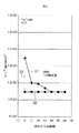
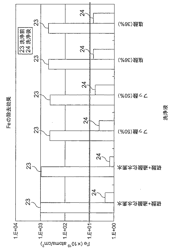
【解決手段】炭化珪素表面における金属不純物濃度が高いこと、その表面金属不純物濃度を1×10¹¹(atoms/cm2)以下にすることにより、実質的に特性の劣化を防止できることを見出した。このような高い清浄度の表面を有する炭化珪素は硫酸と過酸化水素水を含む水溶液を用いて洗浄することによって得られる。
【選択図】 図1
Description
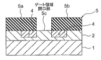
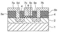
2 エピタキシャル層
3a ソース領域開口部
3b ドレイン領域開口部
3c レジスト
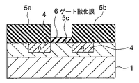
4 ドレイン領域
5,5a,5b 酸化膜
5c ゲート領域開口部
5d,5e 電極開口部
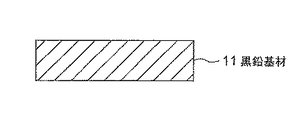
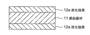
11 黒鉛基材
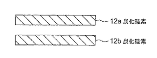
12a,12b 炭化珪素
Claims (5)
- 酸洗浄によって得られ、1×10¹¹(atoms/cm2)以下の金属不純物濃度を有する表面を備え、前記不純物は、鉄、Ni、及び、Cuの少なくとも1種を含む炭化珪素製品であって、前記炭化珪素製品は、炭化珪素半導体装置、半導体装置製造用炭化珪素部材、及び炭化珪素構造物のいずれか一種を含み、前記酸は硫酸と過酸化水素水を含む液であることを特徴とする炭化珪素製品。
- 炭化珪素を酸に浸漬し、表面金属不純物を1×10¹¹(atoms/cm2)以下にする炭化珪素製品の洗浄方法であって、前記炭化珪素製品は、炭化珪素半導体装置、半導体装置製造用炭化珪素部材、及び炭化珪素構造物のいずれか一種を含み、前記金属不純物は、鉄、Ni、及び、Cuの少なくとも一種を含み、前記酸は硫酸と過酸化水素水を含む液であることを特徴とする炭化珪素製品の洗浄方法。
- 炭化珪素を酸で洗浄し、表面金属不純物を1×10¹¹(atoms/cm2)以下にする工程を有する炭化珪素製品の製造方法であって、前記炭化珪素製品は、炭化珪素半導体装置、半導体装置製造用炭化珪素部材、及び炭化珪素構造物のいずれか一種を含み、前記金属不純物は、鉄、Ni、及び、Cuの少なくとも一種を含み、前記酸は硫酸と過酸化水素水を含む液であることを特徴とする炭化珪素製品の製造方法。
- 請求項3において、前記硫酸と過酸化水素水を含む液は4以下のpHを有するように混合されていることを特徴とする炭化珪素製品の製造方法。
- 請求項4において、前記硫酸及び前記過酸化水素水はそれぞれ97%及び30%の濃度を有し、体積比で4:1の比で混合されていることを特徴とする炭化珪素製品の製造方法。
Priority Applications (1)
| Application Number | Priority Date | Filing Date | Title |
|---|---|---|---|
| JP2009223839A JP5033168B2 (ja) | 2009-09-29 | 2009-09-29 | 炭化珪素製品、その製造方法、及び、炭化珪素製品の洗浄方法 |
Applications Claiming Priority (1)
| Application Number | Priority Date | Filing Date | Title |
|---|---|---|---|
| JP2009223839A JP5033168B2 (ja) | 2009-09-29 | 2009-09-29 | 炭化珪素製品、その製造方法、及び、炭化珪素製品の洗浄方法 |
Related Parent Applications (1)
| Application Number | Title | Priority Date | Filing Date |
|---|---|---|---|
| JP2003281801A Division JP2005047753A (ja) | 2003-07-29 | 2003-07-29 | 炭化珪素製品、その製造方法、及び、炭化珪素製品の洗浄方法 |
Publications (2)
| Publication Number | Publication Date |
|---|---|
| JP2010004073A true JP2010004073A (ja) | 2010-01-07 |
| JP5033168B2 JP5033168B2 (ja) | 2012-09-26 |
Family
ID=41585466
Family Applications (1)
| Application Number | Title | Priority Date | Filing Date |
|---|---|---|---|
| JP2009223839A Expired - Fee Related JP5033168B2 (ja) | 2009-09-29 | 2009-09-29 | 炭化珪素製品、その製造方法、及び、炭化珪素製品の洗浄方法 |
Country Status (1)
| Country | Link |
|---|---|
| JP (1) | JP5033168B2 (ja) |
Cited By (6)
| Publication number | Priority date | Publication date | Assignee | Title |
|---|---|---|---|---|
| US10113249B2 (en) | 2014-10-23 | 2018-10-30 | Sumitomo Electric Industries, Ltd. | Silicon carbide substrate and method for manufacturing the same |
| DE112017001570T5 (de) | 2016-03-28 | 2018-12-13 | Sumco Corporation | Verfahren zur Bewertung der Reinheit, Verfahren zur Bestimmung des Reinigungszustandes und Verfahren zur Herstellung von Siliciumwafern |
| KR20190121366A (ko) * | 2017-03-02 | 2019-10-25 | 신에쓰 가가꾸 고교 가부시끼가이샤 | 탄화규소 기판의 제조 방법 및 탄화규소 기판 |
| CN113811643A (zh) * | 2019-05-17 | 2021-12-17 | 住友电气工业株式会社 | 碳化硅衬底 |
| WO2023067876A1 (ja) * | 2021-10-20 | 2023-04-27 | 株式会社サイコックス | 多結晶炭化珪素基板の製造方法 |
| US11646209B2 (en) | 2020-09-22 | 2023-05-09 | Senic Inc. | Method of cleaning wafer and wafer with reduced impurities |
Citations (6)
| Publication number | Priority date | Publication date | Assignee | Title |
|---|---|---|---|---|
| JPH06188163A (ja) * | 1992-12-21 | 1994-07-08 | Toyota Central Res & Dev Lab Inc | 半導体装置作製用SiC単結晶基板とその製造方法 |
| JPH07144999A (ja) * | 1993-11-22 | 1995-06-06 | Denki Kagaku Kogyo Kk | 針状単結晶体及びその製法 |
| JPH0864802A (ja) * | 1994-06-07 | 1996-03-08 | Mitsubishi Materials Corp | 炭化珪素半導体装置及びその製造方法 |
| JPH09153473A (ja) * | 1995-11-30 | 1997-06-10 | Furontetsuku:Kk | ウエット処理方法 |
| JP2000169233A (ja) * | 1998-12-08 | 2000-06-20 | Bridgestone Corp | 炭化ケイ素焼結体の湿式洗浄方法 |
| JP2003142441A (ja) * | 2001-11-02 | 2003-05-16 | Nec Electronics Corp | 洗浄方法および洗浄液 |
-
2009
- 2009-09-29 JP JP2009223839A patent/JP5033168B2/ja not_active Expired - Fee Related
Patent Citations (6)
| Publication number | Priority date | Publication date | Assignee | Title |
|---|---|---|---|---|
| JPH06188163A (ja) * | 1992-12-21 | 1994-07-08 | Toyota Central Res & Dev Lab Inc | 半導体装置作製用SiC単結晶基板とその製造方法 |
| JPH07144999A (ja) * | 1993-11-22 | 1995-06-06 | Denki Kagaku Kogyo Kk | 針状単結晶体及びその製法 |
| JPH0864802A (ja) * | 1994-06-07 | 1996-03-08 | Mitsubishi Materials Corp | 炭化珪素半導体装置及びその製造方法 |
| JPH09153473A (ja) * | 1995-11-30 | 1997-06-10 | Furontetsuku:Kk | ウエット処理方法 |
| JP2000169233A (ja) * | 1998-12-08 | 2000-06-20 | Bridgestone Corp | 炭化ケイ素焼結体の湿式洗浄方法 |
| JP2003142441A (ja) * | 2001-11-02 | 2003-05-16 | Nec Electronics Corp | 洗浄方法および洗浄液 |
Cited By (13)
| Publication number | Priority date | Publication date | Assignee | Title |
|---|---|---|---|---|
| US10704163B2 (en) | 2014-10-23 | 2020-07-07 | Sumitomo Electric Industries, Ltd. | Silicon carbide substrate and method for manufacturing the same |
| US10113249B2 (en) | 2014-10-23 | 2018-10-30 | Sumitomo Electric Industries, Ltd. | Silicon carbide substrate and method for manufacturing the same |
| US11920257B2 (en) | 2016-03-28 | 2024-03-05 | Sumco Corporation | Method of evaluating cleanliness, method of determining cleaning condition, and method of manufacturing silicon wafer |
| DE112017001570T5 (de) | 2016-03-28 | 2018-12-13 | Sumco Corporation | Verfahren zur Bewertung der Reinheit, Verfahren zur Bestimmung des Reinigungszustandes und Verfahren zur Herstellung von Siliciumwafern |
| US11118285B2 (en) | 2016-03-28 | 2021-09-14 | Sumco Corporation | Method of evaluating cleanliness, method of determining cleaning condition, and method of manufacturing silicon wafer |
| KR20190121366A (ko) * | 2017-03-02 | 2019-10-25 | 신에쓰 가가꾸 고교 가부시끼가이샤 | 탄화규소 기판의 제조 방법 및 탄화규소 기판 |
| EP3591101A4 (en) * | 2017-03-02 | 2021-01-13 | Shin-Etsu Chemical Co., Ltd. | MANUFACTURING METHOD FOR A SILICON CARBIDE SUBSTRATE AND SILICON CARBIDE SUBSTRATE |
| KR102473088B1 (ko) | 2017-03-02 | 2022-12-01 | 신에쓰 가가꾸 고교 가부시끼가이샤 | 탄화규소 기판의 제조 방법 및 탄화규소 기판 |
| CN113811643A (zh) * | 2019-05-17 | 2021-12-17 | 住友电气工业株式会社 | 碳化硅衬底 |
| CN113811643B (zh) * | 2019-05-17 | 2024-03-22 | 住友电气工业株式会社 | 碳化硅衬底 |
| US11646209B2 (en) | 2020-09-22 | 2023-05-09 | Senic Inc. | Method of cleaning wafer and wafer with reduced impurities |
| JP2023061509A (ja) * | 2021-10-20 | 2023-05-02 | 株式会社サイコックス | 多結晶炭化珪素基板の製造方法 |
| WO2023067876A1 (ja) * | 2021-10-20 | 2023-04-27 | 株式会社サイコックス | 多結晶炭化珪素基板の製造方法 |
Also Published As
| Publication number | Publication date |
|---|---|
| JP5033168B2 (ja) | 2012-09-26 |
Similar Documents
| Publication | Publication Date | Title |
|---|---|---|
| KR101110984B1 (ko) | 탄화규소 제품, 그의 제조방법 및 탄화규소 제품의세정방법 | |
| JP5033168B2 (ja) | 炭化珪素製品、その製造方法、及び、炭化珪素製品の洗浄方法 | |
| Kuroda et al. | Atomically flat silicon surface and silicon/insulator interface formation technologies for (100) surface orientation large-diameter wafers introducing high performance and low-noise metal–insulator–silicon FETs | |
| JP2009194216A (ja) | 半導体装置の製造方法 | |
| JP2003069012A (ja) | 半導体装置の製造方法 | |
| TW201203391A (en) | Method for manufacturing silicon carbide semiconductor device and apparatus for manufacturing silicon carbide semiconductor device | |
| JP2007053227A (ja) | 半導体素子およびその製造方法 | |
| TW201203385A (en) | Silicon carbide semiconductor device manufacturing method | |
| TW201237968A (en) | Production method for semiconductor device | |
| KR20230132455A (ko) | 에피택셜 웨이퍼의 제조방법 | |
| US20110309376A1 (en) | Method of cleaning silicon carbide semiconductor, silicon carbide semiconductor, and silicon carbide semiconductor device | |
| JP5529217B2 (ja) | 半導体装置の製造方法 | |
| JP2004039946A (ja) | 半導体装置の製造方法 | |
| JP6834932B2 (ja) | 貼り合わせウェーハ用の支持基板の製造方法および貼り合わせウェーハの製造方法 | |
| JP2005079134A (ja) | 半導体基板およびその製造方法 | |
| JP2008159811A (ja) | Soiウェーハの製造方法ならびにsoiウェーハ | |
| TWI273652B (en) | Method of preparing the surface of a Si substrate or layer or source and drain recess of semiconductor elements for depositing an epitaxial layer of SiGe | |
| KR20150003416A (ko) | 실리콘 웨이퍼의 원자 오더 평탄화 표면 처리 방법 및 열처리 장치 | |
| WO1990013912A1 (fr) | Pellicule d'oxyde de silicium et semi-conducteur pourvu de cette pellicule | |
| TW201403719A (zh) | 半導體結構與鍺結構 | |
| JP3565068B2 (ja) | シリコンウエーハの熱処理方法およびシリコンウエーハ | |
| JP6199354B2 (ja) | 半導体装置の製造方法 | |
| JP5298700B2 (ja) | シリコンウェーハの製造方法 | |
| JPH11243093A (ja) | シリコンエピタキシャルウェーハの製造方法 | |
| JPH09199379A (ja) | 高品位エピタキシャルウエハ及びその製造方法 |
Legal Events
| Date | Code | Title | Description |
|---|---|---|---|
| A621 | Written request for application examination |
Free format text: JAPANESE INTERMEDIATE CODE: A621 Effective date: 20090929 |
|
| A521 | Request for written amendment filed |
Free format text: JAPANESE INTERMEDIATE CODE: A821 Effective date: 20090930 |
|
| A977 | Report on retrieval |
Free format text: JAPANESE INTERMEDIATE CODE: A971007 Effective date: 20110316 |
|
| A131 | Notification of reasons for refusal |
Free format text: JAPANESE INTERMEDIATE CODE: A131 Effective date: 20110323 |
|
| A521 | Request for written amendment filed |
Free format text: JAPANESE INTERMEDIATE CODE: A523 Effective date: 20110506 |
|
| A131 | Notification of reasons for refusal |
Free format text: JAPANESE INTERMEDIATE CODE: A131 Effective date: 20111124 |
|
| A521 | Request for written amendment filed |
Free format text: JAPANESE INTERMEDIATE CODE: A523 Effective date: 20120116 |
|
| TRDD | Decision of grant or rejection written | ||
| A01 | Written decision to grant a patent or to grant a registration (utility model) |
Free format text: JAPANESE INTERMEDIATE CODE: A01 Effective date: 20120606 |
|
| A01 | Written decision to grant a patent or to grant a registration (utility model) |
Free format text: JAPANESE INTERMEDIATE CODE: A01 |
|
| A61 | First payment of annual fees (during grant procedure) |
Free format text: JAPANESE INTERMEDIATE CODE: A61 Effective date: 20120629 |
|
| R150 | Certificate of patent or registration of utility model |
Ref document number: 5033168 Country of ref document: JP Free format text: JAPANESE INTERMEDIATE CODE: R150 Free format text: JAPANESE INTERMEDIATE CODE: R150 |
|
| FPAY | Renewal fee payment (event date is renewal date of database) |
Free format text: PAYMENT UNTIL: 20150706 Year of fee payment: 3 |
|
| R250 | Receipt of annual fees |
Free format text: JAPANESE INTERMEDIATE CODE: R250 |
|
| R250 | Receipt of annual fees |
Free format text: JAPANESE INTERMEDIATE CODE: R250 |
|
| R250 | Receipt of annual fees |
Free format text: JAPANESE INTERMEDIATE CODE: R250 |
|
| R250 | Receipt of annual fees |
Free format text: JAPANESE INTERMEDIATE CODE: R250 |
|
| S111 | Request for change of ownership or part of ownership |
Free format text: JAPANESE INTERMEDIATE CODE: R313115 |
|
| S533 | Written request for registration of change of name |
Free format text: JAPANESE INTERMEDIATE CODE: R313533 |
|
| R350 | Written notification of registration of transfer |
Free format text: JAPANESE INTERMEDIATE CODE: R350 |
|
| R250 | Receipt of annual fees |
Free format text: JAPANESE INTERMEDIATE CODE: R250 |
|
| R250 | Receipt of annual fees |
Free format text: JAPANESE INTERMEDIATE CODE: R250 |
|
| S111 | Request for change of ownership or part of ownership |
Free format text: JAPANESE INTERMEDIATE CODE: R313115 |
|
| R371 | Transfer withdrawn |
Free format text: JAPANESE INTERMEDIATE CODE: R371 |
|
| S111 | Request for change of ownership or part of ownership |
Free format text: JAPANESE INTERMEDIATE CODE: R313115 |
|
| R350 | Written notification of registration of transfer |
Free format text: JAPANESE INTERMEDIATE CODE: R350 |
|
| R250 | Receipt of annual fees |
Free format text: JAPANESE INTERMEDIATE CODE: R250 |
|
| R250 | Receipt of annual fees |
Free format text: JAPANESE INTERMEDIATE CODE: R250 |
|
| LAPS | Cancellation because of no payment of annual fees |