JP2009200529A - Method and apparatus for controlling spatial temperature distribution across surface of workpiece support - Google Patents
Method and apparatus for controlling spatial temperature distribution across surface of workpiece support Download PDFInfo
- Publication number
- JP2009200529A JP2009200529A JP2009136934A JP2009136934A JP2009200529A JP 2009200529 A JP2009200529 A JP 2009200529A JP 2009136934 A JP2009136934 A JP 2009136934A JP 2009136934 A JP2009136934 A JP 2009136934A JP 2009200529 A JP2009200529 A JP 2009200529A
- Authority
- JP
- Japan
- Prior art keywords
- temperature
- base element
- chuck assembly
- base
- controlled
- Prior art date
- Legal status (The legal status is an assumption and is not a legal conclusion. Google has not performed a legal analysis and makes no representation as to the accuracy of the status listed.)
- Granted
Links
Images

Classifications
-
- H—ELECTRICITY
- H10—SEMICONDUCTOR DEVICES; ELECTRIC SOLID-STATE DEVICES NOT OTHERWISE PROVIDED FOR
- H10P—GENERIC PROCESSES OR APPARATUS FOR THE MANUFACTURE OR TREATMENT OF DEVICES COVERED BY CLASS H10
- H10P50/00—Etching of wafers, substrates or parts of devices
- H10P50/20—Dry etching; Plasma etching; Reactive-ion etching
- H10P50/24—Dry etching; Plasma etching; Reactive-ion etching of semiconductor materials
- H10P50/242—Dry etching; Plasma etching; Reactive-ion etching of semiconductor materials of Group IV materials
-
- H—ELECTRICITY
- H10—SEMICONDUCTOR DEVICES; ELECTRIC SOLID-STATE DEVICES NOT OTHERWISE PROVIDED FOR
- H10P—GENERIC PROCESSES OR APPARATUS FOR THE MANUFACTURE OR TREATMENT OF DEVICES COVERED BY CLASS H10
- H10P72/00—Handling or holding of wafers, substrates or devices during manufacture or treatment thereof
- H10P72/06—Apparatus for monitoring, sorting, marking, testing or measuring
- H10P72/0602—Temperature monitoring
-
- H—ELECTRICITY
- H10—SEMICONDUCTOR DEVICES; ELECTRIC SOLID-STATE DEVICES NOT OTHERWISE PROVIDED FOR
- H10P—GENERIC PROCESSES OR APPARATUS FOR THE MANUFACTURE OR TREATMENT OF DEVICES COVERED BY CLASS H10
- H10P72/00—Handling or holding of wafers, substrates or devices during manufacture or treatment thereof
- H10P72/04—Apparatus for manufacture or treatment
- H10P72/0431—Apparatus for thermal treatment
- H10P72/0432—Apparatus for thermal treatment mainly by conduction
-
- H—ELECTRICITY
- H01—ELECTRIC ELEMENTS
- H01J—ELECTRIC DISCHARGE TUBES OR DISCHARGE LAMPS
- H01J2237/00—Discharge tubes exposing object to beam, e.g. for analysis treatment, etching, imaging
- H01J2237/20—Positioning, supporting, modifying or maintaining the physical state of objects being observed or treated
- H01J2237/2001—Maintaining constant desired temperature
Landscapes
- Drying Of Semiconductors (AREA)
- Container, Conveyance, Adherence, Positioning, Of Wafer (AREA)
Abstract
【課題】大きいプラズマ熱流束を要せずに、リアクティブ・イオンエッチングの間に半導体ウェーハの温度を制御する方法および装置を提供する。
【解決手段】温度制御型ベース(302)と、断熱材(304)と、平支持体(306)と、ヒータ(308)とを有するプラズマ加工機のチャック。温度制御型ベースは、ワーク(310)の所望温度以下の温度を有する。温度制御型ベース上には断熱材が配置される。断熱材上には平支持体が配置され、該平支持体はワークを保持する。ヒータは、平支持体内に埋設されおよび/または平支持体の下面上に配置される。ヒータは、複数の対応加熱ゾーンを加熱する複数の加熱要素を有している。各加熱要素に供給される電力および/または各加熱要素の温度は独立的に制御される。
【選択図】図1A method and apparatus for controlling the temperature of a semiconductor wafer during reactive ion etching without requiring high plasma heat flux.
A plasma processing machine chuck comprising a temperature control base (302), a heat insulating material (304), a flat support (306), and a heater (308). The temperature controlled base has a temperature below the desired temperature of the workpiece (310). A heat insulating material is disposed on the temperature control type base. A flat support is disposed on the heat insulating material, and the flat support holds the workpiece. The heater is embedded in the flat support and / or arranged on the lower surface of the flat support. The heater has a plurality of heating elements that heat a plurality of corresponding heating zones. The power supplied to each heating element and / or the temperature of each heating element is independently controlled.
[Selection] Figure 1
Description
本発明は基板支持体に関し、より詳しくは、プラズマ加工中に基板内に均一温度分布を達成する方法および装置に関する。 The present invention relates to substrate supports, and more particularly to a method and apparatus for achieving a uniform temperature distribution within a substrate during plasma processing.
一般的なプラズマエッチング装置はリアクタを有し、該リアクタ内には、反応性ガス(単一または複数)が通って流れるチャンバが設けられている。ガスは、このチャンバ内で、一般に高周波エネルギによりプラズマにイオン化される。高い反応性を有するプラズマガスのイオンは、集積回路(IC)に加工される半導体ウェーハの表面上のポリマーマスクのような材料と反応できる。エッチング前に、ウェーハは、チャンバ内に置かれかつチャックまたはホルダにより適正位置に保持されて、ウェーハの上面がプラズマガスに曝される。当該技術分野で知られている幾つかの形式のチャック(時として、サセプタとも呼ばれる)がある。チャックは、等温面を形成しかつウェーハのヒートシンクとして機能する。一形式では、半導体ウェーハは、機械的クランプ手段により、エッチングのための所定位置に保持される。他の形式のチャックでは、半導体ウェーハは、チャックとウェーハとの間で電界により発生される静電力により所定位置に保持される。本発明は両形式のチャックに適用できる。 A typical plasma etching apparatus has a reactor in which a chamber through which reactive gas (s) flows is provided. In this chamber, the gas is generally ionized into plasma by high frequency energy. Highly reactive plasma gas ions can react with materials such as polymer masks on the surface of semiconductor wafers that are processed into integrated circuits (ICs). Prior to etching, the wafer is placed in a chamber and held in place by a chuck or holder so that the top surface of the wafer is exposed to plasma gas. There are several types of chucks (sometimes called susceptors) known in the art. The chuck forms an isothermal surface and functions as a heat sink for the wafer. In one form, the semiconductor wafer is held in place for etching by mechanical clamping means. In other types of chucks, the semiconductor wafer is held in place by an electrostatic force generated by an electric field between the chuck and the wafer. The present invention can be applied to both types of chucks.
一般的なプラズマエッチング作業では、プラズマガスの反応性イオンが、半導体ウェーハの面上の材料の部分と化学的に反応する。ウェーハの或る程度の加熱は幾つかの方法によって行なわれるが、殆どの加熱はプラズマにより行われる。一方、ガス(イオンおよびラジカル)とウェーハ材料との化学反応は、ウェーハの温度上昇により或る程度まで加速される。局部的ウェーハ温度およびウェーハ上の各顕微鏡的箇所での化学反応は、ウェーハ表面を横切る温度が大きく変化する場合に、ウェーハ表面上の材料のエッチングの有害な不均一性が容易に生じる度合いに関係している。殆どの場合、エッチングはほぼ完全な度合いまで均一であることが望まれている。そうでなければ、製造される集積回路デバイスは、望まれる規格から外れた電子的特性をもつものとなってしまうからである。また、ウェーハ直径が増大するにつれて、ICの各バッチの均一性を確保する問題は益々困難になる。他の場合には、カスタムプロファイルを得るには、ウェーハの表面温度を制御できることが望まれている。 In a typical plasma etching operation, the reactive ions of the plasma gas chemically react with the portion of material on the surface of the semiconductor wafer. Some heating of the wafer is done by several methods, but most heating is done by plasma. On the other hand, the chemical reaction between the gas (ions and radicals) and the wafer material is accelerated to a certain extent by the temperature rise of the wafer. The local wafer temperature and the chemical reaction at each microscopic location on the wafer are related to the degree to which deleterious non-uniformities in the etching of materials on the wafer surface can easily occur when the temperature across the wafer surface changes significantly. is doing. In most cases, it is desired that the etching be uniform to an almost perfect degree. Otherwise, the manufactured integrated circuit device will have electronic characteristics that deviate from the desired standard. Also, as the wafer diameter increases, the problem of ensuring the uniformity of each batch of ICs becomes increasingly difficult. In other cases, it is desirable to be able to control the surface temperature of the wafer to obtain a custom profile.
リアクティブ・イオンエッチング(reactive ion etching:RIE)中のウェーハの温度上昇の問題は良く知られており、これまで、エッチング中のウェーハの温度を制御する種々の試みがなされている。図1は、RIE中のウェーハ温度を制御する一方法を示すものである。クーラントガス(例えばヘリウム)が、ウェーハ104の下面と該ウェーハを保持するチャック106の頂部との間の単一狭空間内に、単一圧力で導入される。
The problem of wafer temperature rise during reactive ion etching (RIE) is well known, and various attempts have been made to control the temperature of the wafer during etching. FIG. 1 illustrates one method for controlling wafer temperature during RIE. A coolant gas (eg, helium) is introduced at a single pressure into a single narrow space between the lower surface of the
クーラントの漏洩を低減させるためチャック106の外縁部で1〜5mmの長さで延びている円滑なシーリングランドを除き、一般に、チャックの周囲にはOリングその他のエッジシールは全く設けられていない。必然的に、エラストマーシールがなければ、シーリングランドを横切る漸増する圧力損失があるため、ウェーハ104の縁部の冷却が不充分になる。従って、ウェーハ104の縁部近くに衝突する熱は、該熱がチャックに有効に伝導される前に、半径方向内方に多量に流れなくてはならない。ウェーハ104の上方の矢印108は、ウェーハ104を加熱する進入熱流束を示す。ウェーハ104内の熱の流れが矢印110で示されている。これが、チャックの縁部領域が残りの表面よりも高温になり勝ちな理由である。図2には、ウェーハ104上の典型的な温度分布が示されている。ウェーハ104の周辺部での圧力損失により、ウェーハ104は、周辺部が非常に熱くなる。
In general, there is no O-ring or other edge seal around the chuck, except for a smooth sealing land extending 1-5 mm at the outer edge of the
ゾーンクーリングの必要性に対処する一方法は、表面粗さを変えるか、レリーフパターンをカットして局部的接触領域を有効に変えることである。このようなスキームは裏面クーラントガスを全く使用することなく行なわれ、この場合には、接触領域、表面粗さおよびクランプ力が熱伝達を決定する。しかしながら、局部的接触領域は、チャックを機械加工し直さなくては調節できない。ゾーンクーリングに対処する他の方法は、圧力が変えられるクーラントガスを使用して熱伝達を増大させかつ微調節することである。しかしながら、レリーフパターンは依然として実質的に固定されたままである。仕切り部(dividers)として小さいシーリングランドを用いて(または用いることなく)チャックの表面を異なるゾーンに分割し、かつ各ゾーンに別々の冷却ガスを供給することにより、高度の独立空間制御を達成できる。各ゾーンへのガス供給は、異なる組成にするか異なる圧力に設定して、熱伝導を変えることができる。各ゾーンの作動制御は、配合調節により設定されるか、各加工段階中に動的に安定化される。このようなスキームは、プラズマからの進入熱流束を再分布させかつこれを異なる領域に抽出することに基いて定まる。これは高出力の熱流束には比較的有効であるが、低出力の熱流束には小さい温度差を与えることができるに過ぎない。例えば、約1W/cm2の均一熱流束および約3mmのシーリングランドで、中央部に、ウェーハ周辺部近くで10〜30℃の温度上昇をもたらす縁部熱勾配を与えることができる。この大きさの熱勾配は、プロセス制御パラメータとして非常に有効である。しかしながら、他の加工例えば低出力でのポリゲート加工法は、僅かに0.2W/cm2の熱流束を有する。平均伝導が極めて小さくされない限り(これは、制御が極めて困難でかつ全体的冷却が不充分なものとなる)、一般に5℃以下の非常に小さい温度差になってしまうであろう。 One way to address the need for zone cooling is to change the surface roughness or cut the relief pattern to effectively change the local contact area. Such a scheme is performed without using any backside coolant gas, in which case the contact area, surface roughness and clamping force determine the heat transfer. However, the local contact area cannot be adjusted without reworking the chuck. Another way to deal with zone cooling is to increase and fine-tune heat transfer using a coolant gas whose pressure is varied. However, the relief pattern still remains substantially fixed. Highly independent space control can be achieved by dividing the chuck surface into different zones (with or without) using small sealing lands as dividers and supplying separate cooling gas to each zone . The gas supply to each zone can be set to a different composition or a different pressure to change the heat transfer. The operational control of each zone is set by blending adjustments or dynamically stabilized during each processing stage. Such a scheme is based on redistributing the incoming heat flux from the plasma and extracting it to different regions. This is relatively effective for high power heat flux, but can only provide a small temperature difference for low power heat flux. For example, a uniform heat flux of about 1 W / cm 2 and a sealing land of about 3 mm can provide an edge thermal gradient at the center that results in a 10-30 ° C. temperature increase near the wafer periphery. This magnitude of thermal gradient is very useful as a process control parameter. However, other processes, such as low power polygate processes, have a heat flux of only 0.2 W / cm 2 . Unless the average conduction is made very small (which is very difficult to control and the overall cooling is inadequate), there will generally be a very small temperature difference of 5 ° C. or less.
従って、大きいプラズマ熱流束を要せずして、リアクティブ・イオンエッチングおよび同様な加工法の間に半導体ウェーハの温度を制御する方法および装置が要望されている。本発明の第一目的は、これらの要望を解決しかつ他の関連長所を提供することにある。 Accordingly, there is a need for a method and apparatus for controlling the temperature of a semiconductor wafer during reactive ion etching and similar processing methods without requiring high plasma heat flux. The primary objective of the present invention is to solve these needs and provide other related advantages.
本発明によるプラズマ加工機のチャックは、温度制御型ベースと、断熱材と、平支持体と、ヒータとを有している。温度制御型ベースは、ワークの所望温度以下の温度を有する。温度制御型ベース上には断熱材が配置される。断熱材上には平支持体が配置され、該平支持体はワークを保持する。ヒータは、平支持体内に埋設されおよび/または平支持体の下面上に配置される。ヒータは、複数の対応加熱ゾーンを加熱する複数の加熱要素を有している。各加熱要素に供給される電力および/または各加熱要素の温度は独立的に制御される。 The chuck of the plasma processing machine according to the present invention has a temperature control type base, a heat insulating material, a flat support, and a heater. The temperature control type base has a temperature lower than the desired temperature of the workpiece. A heat insulating material is disposed on the temperature control type base. A flat support is disposed on the heat insulating material, and the flat support holds the workpiece. The heater is embedded in the flat support and / or arranged on the lower surface of the flat support. The heater has a plurality of heating elements that heat a plurality of corresponding heating zones. The power supplied to each heating element and / or the temperature of each heating element is independently controlled.
本願明細書に組込まれかつこの一部を形成する添付図面は、本発明の1以上の実施形態を示しかつ詳細な説明と相俟って本発明の原理および実施を説明する機能を有している。
本発明の実施形態は、ワーク支持体の表面を横切る空間温度分布を制御する方法および装置に関連して説明する。当業者ならば、本発明の以下の詳細な説明は単なる例示であって、いかなる制限をも意味するものではないことが理解されよう。本発明の他の実施形態は、本願の開示に利益を有する当業者にとっては容易に示唆されるものである。本発明の実施には、添付図面に示されたものを詳細に参照されたい。全図面および以下の詳細な説明を通して、同じまたは同類の部品には同じ参照番号が使用されている。
The accompanying drawings, which are incorporated in and form a part of this specification, illustrate one or more embodiments of the invention and, together with the detailed description, have the capability to explain the principles and implementations of the invention. Yes.
Embodiments of the present invention are described in the context of a method and apparatus for controlling the spatial temperature distribution across the surface of a workpiece support. Those skilled in the art will appreciate that the following detailed description of the present invention is illustrative only and is not meant to be in any way limiting. Other embodiments of the invention will be readily suggested to one of ordinary skill in the art having the benefit of this disclosure. Reference will now be made in detail to implementations of the present invention as illustrated in the accompanying drawings. Throughout the drawings and the following detailed description, the same reference numbers are used for the same or similar parts.
明瞭化の観点で、実施上の必ずしも全ての特徴が図示および説明されてはいない。このようなあらゆる実際上の実施を行なうに際し、用途への追従および商業上の拘束等の開発者の特定目的を達成するには実施する上での多くの特定決定を行なう必要があること、およびこれらの特定目的は一実施から他の実施へと、および一開発者から他の開発者へと変わることは、もちろん理解されよう。また、このような開発努力は複雑で時間を要するものであるが、本願開示の利益を有する当業者は工学的に事業化できるであろう。 Not all features of an implementation are shown and described for clarity. In making any such practical implementation, many specific decisions must be made in order to achieve the specific purpose of the developer, such as following applications and commercial restraints, and It will of course be understood that these specific objectives will change from one implementation to another, and from one developer to another. Also, such development efforts are complex and time consuming, but those skilled in the art having the benefit of this disclosure will be able to commercialize engineering.
本発明の装置は、例えば5℃を超える正確な大きい温度差を達成することを探求するものであるが、例えば2W/cm2以下のように、大きいプラズマ熱流束を必要としないものである。図3Aは、本発明の一実施形態によるワーク温度制御装置を示す概略側面図である。ベース302すなわち熱交換器が断熱材304を支持している。該断熱材304上には、好ましくは平支持体306が取付けられている。支持体306内には、ヒータ308が埋設されている。支持体306上には、ウェーハのようなワーク310が配置されている。熱伝導体312が、支持体306とワーク310との間の熱的密接を形成している。熱伝導体312は、ヘリウムのようなガスが好ましい。ヘリウム圧力は、ワーク310と支持体306との熱伝導を制御する。
The apparatus of the present invention seeks to achieve an accurate large temperature difference, for example exceeding 5 ° C., but does not require a large plasma heat flux, for example 2 W / cm 2 or less. FIG. 3A is a schematic side view showing a workpiece temperature control apparatus according to an embodiment of the present invention. A base 302 or heat exchanger supports the
一実施形態によれば、ベース302は、冷却/加熱流体ループのような慣用の熱交換システムを通して比較的一定温度に維持される金属材料(好ましくはアルミニウムベースの冷却板)で構成される。他の実施形態によれば、ベース302は、窒化アルミニウムのような非金属材料で構成することもできる。しかしながら、ベース302は、ヒータ308を用いない標準的作動時におけるよりも大きく冷却されなければならない。例えば、ベース302の温度は、ワーク310の所望温度よりも10〜50℃低くすることができる。ベース302はまた、プラズマ加熱の場合の熱シンクを形成する。ベースプレート302の温度を維持するため、外部クーラント冷却器(図示せず)を使用することもできる。外部クーラント冷却器により除去される熱量およびクーラントの温度は、それぞれ、2000Wおよび−20℃以下に制限できる。ベース302には、ヒータ用給電線312または他のサービスラインを配置するための幾つかの孔およびキャビティ(図示せず)を設けることができる。このようなサービスラインとして、ヒータ、センサ、高電圧静電クランプ用の給電線がある。当業者ならば、サービスラインは前掲のものに限定されないことは理解されよう。
According to one embodiment, the
一実施形態によれば、断熱材304は、支持体306とベース302との間の大きい熱インピーダンス断熱層(thermal impedance break)として機能する。断熱材304は、ポリマー、プラスチックまたはセラミックで作られた厚いRTV接着層で構成できる。しかしながら、断熱材304の熱インピーダンス断熱層は、ウェーハ310の冷却が不充分になるほど過度のものであってはならない。例えば、断熱材は、約0.05〜0.20W/mKの範囲の熱伝導率を有するのが好ましい。この場合、断熱材304は、耐熱要素として、および支持体306とベース302との接合材としての両機能を有する。また、断熱材304は、プラズマとベース304との間に充分なRFカップリングが維持されるものでなくてはならない。また、断熱材304は、層の上下に存在する異なる材料および温度による大きい熱−機械的剪断を許容できなくてはならない。一実施形態によれば、断熱材304の厚さは2mm以下にすべきである。断熱材304には、ヒータ用給電線312および他のサービスラインを収容するための、ベース304のキャビティに隣接する幾つかのキャビティまたはバイア(vias)(図示せず)を設けることができる。
According to one embodiment, the
一実施形態によれば、支持体306はセラミック材料で構成される。セラミックは、例えばアルミナのような非導電性材料で形成できる。支持体306の形状は、プラズマエッチングシステムに一般的に使用されている慣用ディスクにするのが好ましい。ワーク306は慣用の静電チャックで構成するか、ウェーハ310を保持する機械的クランプを備えたセラミックで構成できる。一実施形態によれば、支持体306の厚さは約2mmである。しかしながら、当業者ならば、他の厚さも適していることは理解されよう。他の実施形態によれば、支持体306の構造は「ベースに接合された薄いディスク」であり、そうでなければ、側方熱伝導が非常に高くなり、ヒータ入力が側方に拡大されてゾーン分離が非効率的になってしまう。支持体は、熱を局部的に散逸させることができる。
According to one embodiment, the
ヒータ308は、少なくとも1つの抵抗要素を有している。一実施形態によれば、ヒータ308は、クランプ電極平面の下で支持体306内に埋設でき、かつ例えば対称的または任意の所望パターンの形状にすることができる。ヒータ308は、1以上の平加熱要素で構成することもできる。各加熱要素は、独立的に制御される加熱ゾーンまたは領域を形成する。多ゾーンパターンは、支持体306への伝導冷却(conduction cooling)とは逆に作用する1以上の平加熱要素を有している。各加熱ゾーンに関連するセンサ309は、各加熱ゾーンの温度を測定しかつ信号をコントローラまたはコンピュータ(図7参照)に送って、個々の平加熱要素をモニタしかつ制御する。例えば、赤外線放射センサまたは熱電対センサ等のセンサは、ワーク310から直接読取りできるようにポートを通して取付けることができる。センサ309は支持体306内または背面に取付けることもできる。ヒータ308には、断熱材304およびベース302の開口を通って配置される給電線312により給電できる。
The
一実施形態によれば、ヒータ308は誘導ヒータで構成される。他の実施形態によれば、ヒータ308は、クリプトンランプまたは石英ランプ等の加熱ランプで構成される。更に別の実施形態によれば、ヒータ308は、冷却または加熱が可能な熱電モジュールで構成できる。熱電モジュールを用いる場合には、ベースまたは断熱層は任意に構成できる。当業者ならば、支持体306を加熱するのに他の多くの方法があることは理解されよう。
According to one embodiment, the
図3Bには、本発明の他の実施形態が示されている。図3Bの実施形態では、ヒータ308は、薄膜ヒータのような蝕刻箔技術で形成される。ヒータ308はワーク支持体306内に埋設するか、ワーク支持体306の背面上に取付けることができる(図示せず)。断熱材304と支持体306との間および断熱材304とベース302との間には、ポリマーのような接合層(図示せず。各層の厚さは例えば0.003インチである)が配置される。
FIG. 3B shows another embodiment of the present invention. In the embodiment of FIG. 3B, the
図3Cは、図3Aの装置における熱流量力学を示す簡単化された概略図である。進入するプラズマ熱流束Q1は、ウェーハ310の表面上の温度T1に寄与する。ヒータ308は、ウェーハ310に熱Q3を供給する。ワーク支持体306を通り冷却されたベース302に入る、システムからの外出熱流束Q2は、進入熱流束Q1およびQ3の合計にほぼ等しく、従って次式のように表される。
Q1+Q3=Q2
定義により、ウェーハ310の温度T1と、断熱材304を通る温度ΔTとの合計は、冷却されたベース302の温度T1に等しい。
T1=T2+ΔT
ΔTは、断熱材304の熱伝導率により定められることに留意されたい。かくして、ヒータ308により発生される進入熱流束Q3はΔTを制御する。従って、ヒータ308の出力は、Q1の範囲でウェーハの表面上に所望温度T1が得られるように調節される。
FIG. 3C is a simplified schematic diagram illustrating thermal flow dynamics in the apparatus of FIG. 3A. The incoming plasma heat flux Q1 contributes to the temperature T1 on the surface of the
Q1 + Q3 = Q2
By definition, the sum of the temperature T 1 of the
T1 = T2 + ΔT
Note that ΔT is determined by the thermal conductivity of the
好ましくは、ベース302の温度は、進入熱流束Q1が存在せず、かつ最大熱流束Q3が最大熱流束Q1にほぼ等しいとき、最大進入熱流束Q3の約1/2の外出熱流束Q2を発生するように設定される。すなわち、
Q1=0でありかつQ3max≒Q1maxであるとき、
Q2≒1/2・Q3max
Preferably, the temperature of the
When Q1 = 0 and Q3 max ≈Q1 max ,
Q2 ≒ 1/2 ・ Q3 max
この好ましいスキームでは、T1が変化できる範囲は最大化される。すなわち、ウェーハの局部的温度は、ヒータ308のゾーンの加熱出力を制御することにより調節できる。一実施形態によれば、ベース302の温度すなわちクーラント温度は、最大値Q1と最大値Q3との合計が最大値Q2に等しくなる慣用装置よりも約20℃低く設定される。
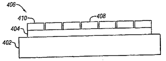
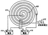
ここで図4Aの概略側面図を参照すると、ここには、本発明の他の実施形態に従ってワークの温度を制御する一体型単一平層電極/ヒータを備えた装置が示されている。ベース402は断熱材404を支持している。断熱材404上には平支持体406が取付けられている。一実施形態によれば、平支持体406は内側スパイラル408および外側スパイラル410を有し、これらの両スパイラル408、410は、ワークおよびワークをクランプする電極を加熱するヒータとして使用される。両ヒータおよび電極は、平支持体406により表される単一平層構造を形成するように一体化されている。図4Bは平支持体406の平面図である。内側スパイラル408と外側スパイラル410との間には差動高電圧HV412が印加され、平支持体406の静電クランプ機能を発生させる。差動高電圧HV412がアース(接地)に対して内側スパイラル408および外側スパイラル410の両者に印加される場合には、平支持体406は単極静電チャックとして機能する。差動高電圧HVが内側スパイラル408と外側スパイラル410との間に印加される場合には、平支持体406は双極チャックとして機能する。内側コイル408には第一制御電源414が接続され、第一加熱ゾーンを発生させる。外側コイル410には第二制御電源414が接続され、第二加熱ゾーンを発生させる。
In this preferred scheme, the range over which T1 can be varied is maximized. That is, the local temperature of the wafer can be adjusted by controlling the heating power of the
Referring now to the schematic side view of FIG. 4A, there is shown an apparatus with an integrated single flat layer electrode / heater that controls the temperature of the workpiece in accordance with another embodiment of the present invention. The
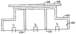
図5は、本発明の他の実施形態による側方断熱層(lateral thermal break)アプローチを用いたワーク温度制御装置を示す概略側面図である。直接電気加熱または異なる温度のクーラントを用いる代わりに二重または多重マニホルドヒートシンクを用いて、温度制御された流体を循環させることができる。温度制御されるベース502が、断熱材(例えばセラミック)504を支持する。平支持体506がワーク508の支持体を形成する。ベース502は、断熱材510により、2以上のゾーンに方位角的に分離されており、各ゾーンがヒートシンクを表している。矢印は異なるヒートシンクゾーンを表している。より詳しくは、側方断熱層510が、ヒートシンクを2以上のサーマルゾーン、例えばゾーンT1、T2に分離している。各サーマルゾーンの温度は、各流体ループ内の流体温度を制御することにより独立的に制御できる。このような断熱層510の使用により、任意の空間ゾーンを考慮に入れることができる。
FIG. 5 is a schematic side view illustrating a workpiece temperature control apparatus using a lateral thermal break approach according to another embodiment of the present invention. Instead of using direct electrical heating or different temperature coolants, dual or multiple manifold heat sinks can be used to circulate the temperature controlled fluid. A temperature controlled
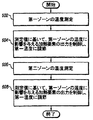
図6は、本発明の一実施形態によるチャックの温度を制御する方法を示すフローチャートである。より詳しくは、図6は、2つの別個のサーマルゾーンを備えたチャックの温度制御方法を示すものである。当業者ならば、本発明の方法が1以上のサーマルゾーンを有するチャックに適用できることが理解されよう。第一ブロック602では、第一組のセンサを用いて第一ゾーンの温度が測定される。これらの測定値に基いて、ブロック604では、第一ゾーンの温度に影響を与える加熱要素の出力を制御して、第一ゾーンの温度を、ユーザおよび/またはコンピュータにより設定された温度に調節する。第二ブロック606では、第二組のセンサを用いて第二ゾーンの温度が測定される。これらの測定値に基いて、ブロック608では、第二ゾーンの温度に影響を与える加熱要素の出力を制御して、第二ゾーンの温度を、ユーザおよび/またはコンピュータにより設定された温度に調節する。
FIG. 6 is a flowchart illustrating a method for controlling the temperature of a chuck according to an embodiment of the present invention. More specifically, FIG. 6 shows a temperature control method for a chuck with two separate thermal zones. One skilled in the art will appreciate that the method of the present invention is applicable to chucks having one or more thermal zones. In a
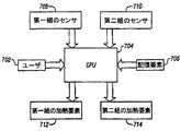
図7は、本発明の一実施形態によるチャックの温度制御システムを示す概略図である。ユーザ702はコンピュータ704に1組のパラメータを入力する。このようなパラメータの組として、例えば、チャックの第一ゾーンの所望温度およびチャックの第二ゾーンの所望温度がある。当業者ならば、チャックに1以上のゾーンを設けることができることは理解されよう。コンピュータ704は、図6のアルゴリズム、コンピュータ704の入力および出力を記憶している記憶要素706と通信する。第一組のセンサ708がチャックの第一ゾーンを測定し、第2組のセンサ710がチャックの第二ゾーンを測定する。第一組のセンサ708の温度測定値に基いて、コンピュータ704は、第一組の加熱要素712を制御してチャックの第一ゾーンの温度を調節する。第二組のセンサ710の温度測定値に基いて、コンピュータ704は、第二組の加熱要素714を制御してチャックの第二ゾーンの温度を調節する。
FIG. 7 is a schematic diagram illustrating a chuck temperature control system according to an embodiment of the present invention.
静電チャック上のウェーハの温度分布を制御する上記方法は、誘導結合プラズマ(Inductive Coupled Plasma:ICP)加工機での適用に適しているだけでなく、特に、ウェーハへの低プラズマ出力熱流束を必要とする他の任意のシステムへの用途にも適している。この技術は、本発明の技術は、熱勾配を形成する必要性が存在する他の任意の用途に適用できる。 The above method for controlling the temperature distribution of the wafer on the electrostatic chuck is not only suitable for application in an inductive coupled plasma (ICP) processing machine, but in particular a low plasma output heat flux to the wafer. It is also suitable for use in any other system that requires it. This technique can be applied to any other application where there is a need for the technique of the present invention to form a thermal gradient.
以上、本発明の実施形態および用途を図示しかつ説明したが、本願開示の利益を有する当業者ならば、本発明の概念から逸脱することなく、上記以外の多くの変更形態を想到し得ることは明白である。従って本発明は、特許請求の範囲に記載の精神を除き、いかなる制限を受けるものではない。 While the embodiments and applications of the present invention have been illustrated and described, those skilled in the art having the benefit of this disclosure may conceive many other variations without departing from the concept of the present invention. Is obvious. Accordingly, the invention is not limited in any way except by the spirit described in the claims.
302 ベース
304 断熱材
306 支持体
308ヒータ
310 ワーク(ウェーハ)
412 差動高電圧
414 第一ヒータ電源
416 第二ヒータ電源
302
412 Differential high voltage 414 1st heater power supply 416 2nd heater power supply
Claims (8)
ワークを支持する支持要素と、
前記支持要素の下方に配置され、前記支持体に熱的に結合された単一部品ベース要素と、を含み、前記ベース要素は、該ベース要素の表面上に配置された連続的な断熱材の層を有し、前記ベース要素は、少なくとも1つの側方断熱層によって少なくとも2つの温度制御される部分に分離されており、その1つの温度制御される部分は、ディスク形状であり、周囲部分は、前記支持要素を超えて延びており、各温度制御される部分は、該各温度制御される部分に関連した流体ループを通して温度制御された流体を循環させることによって独立して熱的制御可能であることを特徴とするチャック組立体。 A chuck assembly for a plasma processing machine, the chuck assembly comprising:
A support element for supporting the workpiece;
A single component base element disposed below the support element and thermally coupled to the support, the base element comprising a continuous insulation disposed on a surface of the base element The base element is separated into at least two temperature controlled parts by at least one lateral thermal insulation layer, the one temperature controlled part being disc-shaped and the surrounding part being Each temperature controlled portion can be independently thermally controlled by circulating a temperature controlled fluid through a fluid loop associated with each temperature controlled portion. A chuck assembly comprising:
対応する部分の各々に関連した流体ループを通して温度制御された流体を循環させて、チャック組立体の支持要素であって、該支持要素は、前記ベース要素の上方に配置され、前記ベース要素に熱的に結合されている支持要素上に配置されたワークの温度を制御する、ことを特徴とする方法。 A fluid temperature is measured corresponding to each of the two or more portions of the single part base element of the chuck assembly, the base element having a continuous layer of thermal insulation disposed on the surface of the base element. The base element is separated into at least two temperature-controlled parts by at least one side thermal insulation layer, the one temperature-controlled part being disc-shaped and the surrounding part being the support element Each temperature controlled portion is independently thermally controllable by circulating a temperature controlled fluid through a fluid loop associated with each temperature controlled portion;
Circulating a temperature-controlled fluid through a fluid loop associated with each of the corresponding portions to provide a support element for the chuck assembly, the support element being disposed above the base element and providing heat to the base element. Controlling the temperature of a workpiece placed on a support element that is mechanically coupled.
Applications Claiming Priority (4)
| Application Number | Priority Date | Filing Date | Title |
|---|---|---|---|
| US84643201A | 2001-04-30 | 2001-04-30 | |
| US09/846,432 | 2001-04-30 | ||
| US10/062,395 US6847014B1 (en) | 2001-04-30 | 2002-02-01 | Method and apparatus for controlling the spatial temperature distribution across the surface of a workpiece support |
| US10/062,395 | 2002-02-01 |
Related Parent Applications (1)
| Application Number | Title | Priority Date | Filing Date |
|---|---|---|---|
| JP2002586683A Division JP4549022B2 (en) | 2001-04-30 | 2002-04-23 | Method and apparatus for controlling spatial temperature distribution across the surface of a workpiece support |
Publications (2)
| Publication Number | Publication Date |
|---|---|
| JP2009200529A true JP2009200529A (en) | 2009-09-03 |
| JP5388704B2 JP5388704B2 (en) | 2014-01-15 |
Family
ID=34063657
Family Applications (1)
| Application Number | Title | Priority Date | Filing Date |
|---|---|---|---|
| JP2009136934A Expired - Lifetime JP5388704B2 (en) | 2001-04-30 | 2009-06-08 | Method and apparatus for controlling spatial temperature distribution across the surface of a workpiece support |
Country Status (4)
| Country | Link |
|---|---|
| US (1) | US6847014B1 (en) |
| JP (1) | JP5388704B2 (en) |
| KR (1) | KR100880132B1 (en) |
| CN (1) | CN101335186B (en) |
Families Citing this family (486)
| Publication number | Priority date | Publication date | Assignee | Title |
|---|---|---|---|---|
| US20050211385A1 (en) * | 2001-04-30 | 2005-09-29 | Lam Research Corporation, A Delaware Corporation | Method and apparatus for controlling spatial temperature distribution |
| US7161121B1 (en) * | 2001-04-30 | 2007-01-09 | Lam Research Corporation | Electrostatic chuck having radial temperature control capability |
| WO2002089531A1 (en) * | 2001-04-30 | 2002-11-07 | Lam Research, Corporation | Method and apparatus for controlling the spatial temperature distribution across the surface of a workpiece support |
| TWI246873B (en) * | 2001-07-10 | 2006-01-01 | Tokyo Electron Ltd | Plasma processing device |
| US7347901B2 (en) * | 2002-11-29 | 2008-03-25 | Tokyo Electron Limited | Thermally zoned substrate holder assembly |
| KR100904361B1 (en) * | 2003-03-28 | 2009-06-23 | 도쿄엘렉트론가부시키가이샤 | Method and system for temperature control of a substrate |
| US8038796B2 (en) | 2004-12-30 | 2011-10-18 | Lam Research Corporation | Apparatus for spatial and temporal control of temperature on a substrate |
| US20070082313A1 (en) * | 2005-08-04 | 2007-04-12 | Katsuhiro Itakura | Wafer holder, heater unit having the wafer holder, and wafer prober having the heater unit |
| US7525787B2 (en) * | 2005-09-30 | 2009-04-28 | Lam Research Corporation | Electrostatic chuck assembly with dielectric material and/or cavity having varying thickness, profile and/or shape, method of use and apparatus incorporating same |
| US7869184B2 (en) * | 2005-11-30 | 2011-01-11 | Lam Research Corporation | Method of determining a target mesa configuration of an electrostatic chuck |
| US8226769B2 (en) * | 2006-04-27 | 2012-07-24 | Applied Materials, Inc. | Substrate support with electrostatic chuck having dual temperature zones |
| US7501605B2 (en) * | 2006-08-29 | 2009-03-10 | Lam Research Corporation | Method of tuning thermal conductivity of electrostatic chuck support assembly |
| US7297894B1 (en) | 2006-09-25 | 2007-11-20 | Tokyo Electron Limited | Method for multi-step temperature control of a substrate |
| US7838800B2 (en) * | 2006-09-25 | 2010-11-23 | Tokyo Electron Limited | Temperature controlled substrate holder having erosion resistant insulating layer for a substrate processing system |
| US7557328B2 (en) * | 2006-09-25 | 2009-07-07 | Tokyo Electron Limited | High rate method for stable temperature control of a substrate |
| US7723648B2 (en) * | 2006-09-25 | 2010-05-25 | Tokyo Electron Limited | Temperature controlled substrate holder with non-uniform insulation layer for a substrate processing system |
| US8986456B2 (en) * | 2006-10-10 | 2015-03-24 | Asm America, Inc. | Precursor delivery system |
| US7541290B2 (en) * | 2007-03-08 | 2009-06-02 | Samsung Electronics Co., Ltd. | Methods of forming mask patterns on semiconductor wafers that compensate for nonuniform center-to-edge etch rates during photolithographic processing |
| US8083855B2 (en) | 2007-10-31 | 2011-12-27 | Lam Research Corporation | Temperature control module using gas pressure to control thermal conductance between liquid coolant and component body |
| US10378106B2 (en) | 2008-11-14 | 2019-08-13 | Asm Ip Holding B.V. | Method of forming insulation film by modified PEALD |
| KR101691044B1 (en) * | 2009-02-04 | 2016-12-29 | 맷슨 테크놀로지, 인크. | Electrostatic chuck system and process for radially tuning the temperature profile across the surface of a substrate |
| US9394608B2 (en) | 2009-04-06 | 2016-07-19 | Asm America, Inc. | Semiconductor processing reactor and components thereof |
| US8802201B2 (en) | 2009-08-14 | 2014-08-12 | Asm America, Inc. | Systems and methods for thin-film deposition of metal oxides using excited nitrogen-oxygen species |
| US8883270B2 (en) * | 2009-08-14 | 2014-11-11 | Asm America, Inc. | Systems and methods for thin-film deposition of metal oxides using excited nitrogen—oxygen species |
| US8877655B2 (en) | 2010-05-07 | 2014-11-04 | Asm America, Inc. | Systems and methods for thin-film deposition of metal oxides using excited nitrogen-oxygen species |
| US8637794B2 (en) | 2009-10-21 | 2014-01-28 | Lam Research Corporation | Heating plate with planar heating zones for semiconductor processing |
| US8522569B2 (en) * | 2009-10-27 | 2013-09-03 | Industrial Idea Partners, Inc. | Utilization of data center waste heat for heat driven engine |
| KR101841378B1 (en) | 2009-12-15 | 2018-03-22 | 램 리써치 코포레이션 | Adjusting substrate temperature to improve cd uniformity |
| EP2383771B1 (en) * | 2010-04-29 | 2020-04-22 | EV Group GmbH | Method and device for loosening a polymer coating from a surface of a substrate |
| US8410393B2 (en) | 2010-05-24 | 2013-04-02 | Lam Research Corporation | Apparatus and method for temperature control of a semiconductor substrate support |
| US8529729B2 (en) | 2010-06-07 | 2013-09-10 | Lam Research Corporation | Plasma processing chamber component having adaptive thermal conductor |
| US9171702B2 (en) | 2010-06-30 | 2015-10-27 | Lam Research Corporation | Consumable isolation ring for movable substrate support assembly of a plasma processing chamber |
| US8826855B2 (en) | 2010-06-30 | 2014-09-09 | Lam Research Corporation | C-shaped confinement ring for a plasma processing chamber |
| US8485128B2 (en) | 2010-06-30 | 2013-07-16 | Lam Research Corporation | Movable ground ring for a plasma processing chamber |
| US20120012299A1 (en) * | 2010-07-16 | 2012-01-19 | Industrial Idea Partners, Inc. | Proportional Micro-Valve With Thermal Feedback |
| US9728429B2 (en) | 2010-07-27 | 2017-08-08 | Lam Research Corporation | Parasitic plasma prevention in plasma processing chambers |
| US8791392B2 (en) | 2010-10-22 | 2014-07-29 | Lam Research Corporation | Methods of fault detection for multiplexed heater array |
| US8546732B2 (en) | 2010-11-10 | 2013-10-01 | Lam Research Corporation | Heating plate with planar heater zones for semiconductor processing |
| US9312155B2 (en) | 2011-06-06 | 2016-04-12 | Asm Japan K.K. | High-throughput semiconductor-processing apparatus equipped with multiple dual-chamber modules |
| US9793148B2 (en) | 2011-06-22 | 2017-10-17 | Asm Japan K.K. | Method for positioning wafers in multiple wafer transport |
| US10364496B2 (en) | 2011-06-27 | 2019-07-30 | Asm Ip Holding B.V. | Dual section module having shared and unshared mass flow controllers |
| US10854498B2 (en) | 2011-07-15 | 2020-12-01 | Asm Ip Holding B.V. | Wafer-supporting device and method for producing same |
| US8520360B2 (en) | 2011-07-19 | 2013-08-27 | Lam Research Corporation | Electrostatic chuck with wafer backside plasma assisted dechuck |
| US20130023129A1 (en) | 2011-07-20 | 2013-01-24 | Asm America, Inc. | Pressure transmitter for a semiconductor processing environment |
| US9307578B2 (en) | 2011-08-17 | 2016-04-05 | Lam Research Corporation | System and method for monitoring temperatures of and controlling multiplexed heater array |
| US10388493B2 (en) | 2011-09-16 | 2019-08-20 | Lam Research Corporation | Component of a substrate support assembly producing localized magnetic fields |
| US8624168B2 (en) | 2011-09-20 | 2014-01-07 | Lam Research Corporation | Heating plate with diode planar heater zones for semiconductor processing |
| US8461674B2 (en) | 2011-09-21 | 2013-06-11 | Lam Research Corporation | Thermal plate with planar thermal zones for semiconductor processing |
| US9341296B2 (en) | 2011-10-27 | 2016-05-17 | Asm America, Inc. | Heater jacket for a fluid line |
| US9096931B2 (en) | 2011-10-27 | 2015-08-04 | Asm America, Inc | Deposition valve assembly and method of heating the same |
| US9017481B1 (en) | 2011-10-28 | 2015-04-28 | Asm America, Inc. | Process feed management for semiconductor substrate processing |
| US9005539B2 (en) | 2011-11-23 | 2015-04-14 | Asm Ip Holding B.V. | Chamber sealing member |
| US9167625B2 (en) | 2011-11-23 | 2015-10-20 | Asm Ip Holding B.V. | Radiation shielding for a substrate holder |
| US9324589B2 (en) | 2012-02-28 | 2016-04-26 | Lam Research Corporation | Multiplexed heater array using AC drive for semiconductor processing |
| US9202727B2 (en) * | 2012-03-02 | 2015-12-01 | ASM IP Holding | Susceptor heater shim |
| US8946830B2 (en) | 2012-04-04 | 2015-02-03 | Asm Ip Holdings B.V. | Metal oxide protective layer for a semiconductor device |
| US8809747B2 (en) | 2012-04-13 | 2014-08-19 | Lam Research Corporation | Current peak spreading schemes for multiplexed heated array |
| US9029253B2 (en) | 2012-05-02 | 2015-05-12 | Asm Ip Holding B.V. | Phase-stabilized thin films, structures and devices including the thin films, and methods of forming same |
| US8728832B2 (en) | 2012-05-07 | 2014-05-20 | Asm Ip Holdings B.V. | Semiconductor device dielectric interface layer |
| NL2010642A (en) | 2012-05-17 | 2013-11-20 | Asml Netherlands Bv | Thermal conditioning unit, lithographic apparatus and device manufacturing method. |
| US8933375B2 (en) | 2012-06-27 | 2015-01-13 | Asm Ip Holding B.V. | Susceptor heater and method of heating a substrate |
| US9558931B2 (en) | 2012-07-27 | 2017-01-31 | Asm Ip Holding B.V. | System and method for gas-phase sulfur passivation of a semiconductor surface |
| US9117866B2 (en) | 2012-07-31 | 2015-08-25 | Asm Ip Holding B.V. | Apparatus and method for calculating a wafer position in a processing chamber under process conditions |
| US9659799B2 (en) | 2012-08-28 | 2017-05-23 | Asm Ip Holding B.V. | Systems and methods for dynamic semiconductor process scheduling |
| US9169975B2 (en) | 2012-08-28 | 2015-10-27 | Asm Ip Holding B.V. | Systems and methods for mass flow controller verification |
| US9021985B2 (en) | 2012-09-12 | 2015-05-05 | Asm Ip Holdings B.V. | Process gas management for an inductively-coupled plasma deposition reactor |
| US9018022B2 (en) | 2012-09-24 | 2015-04-28 | Lam Research Corporation | Showerhead electrode assembly in a capacitively coupled plasma processing apparatus |
| US9324811B2 (en) | 2012-09-26 | 2016-04-26 | Asm Ip Holding B.V. | Structures and devices including a tensile-stressed silicon arsenic layer and methods of forming same |
| US10714315B2 (en) | 2012-10-12 | 2020-07-14 | Asm Ip Holdings B.V. | Semiconductor reaction chamber showerhead |
| US10049948B2 (en) | 2012-11-30 | 2018-08-14 | Lam Research Corporation | Power switching system for ESC with array of thermal control elements |
| US10177014B2 (en) | 2012-12-14 | 2019-01-08 | Applied Materials, Inc. | Thermal radiation barrier for substrate processing chamber components |
| US9640416B2 (en) | 2012-12-26 | 2017-05-02 | Asm Ip Holding B.V. | Single-and dual-chamber module-attachable wafer-handling chamber |
| US20160376700A1 (en) | 2013-02-01 | 2016-12-29 | Asm Ip Holding B.V. | System for treatment of deposition reactor |
| US8894870B2 (en) | 2013-02-01 | 2014-11-25 | Asm Ip Holding B.V. | Multi-step method and apparatus for etching compounds containing a metal |
| US20140251214A1 (en) * | 2013-03-06 | 2014-09-11 | Applied Materials, Inc. | Heated substrate support with flatness control |
| US9484191B2 (en) | 2013-03-08 | 2016-11-01 | Asm Ip Holding B.V. | Pulsed remote plasma method and system |
| US9589770B2 (en) | 2013-03-08 | 2017-03-07 | Asm Ip Holding B.V. | Method and systems for in-situ formation of intermediate reactive species |
| US9666466B2 (en) * | 2013-05-07 | 2017-05-30 | Applied Materials, Inc. | Electrostatic chuck having thermally isolated zones with minimal crosstalk |
| JP6075555B2 (en) * | 2013-07-05 | 2017-02-08 | 日新イオン機器株式会社 | Electrostatic chuck system and semiconductor manufacturing apparatus |
| US8993054B2 (en) | 2013-07-12 | 2015-03-31 | Asm Ip Holding B.V. | Method and system to reduce outgassing in a reaction chamber |
| US9018111B2 (en) | 2013-07-22 | 2015-04-28 | Asm Ip Holding B.V. | Semiconductor reaction chamber with plasma capabilities |
| KR20180110213A (en) * | 2013-08-06 | 2018-10-08 | 어플라이드 머티어리얼스, 인코포레이티드 | Locally heated multi-zone substrate support |
| US9396934B2 (en) | 2013-08-14 | 2016-07-19 | Asm Ip Holding B.V. | Methods of forming films including germanium tin and structures and devices including the films |
| US9793115B2 (en) | 2013-08-14 | 2017-10-17 | Asm Ip Holding B.V. | Structures and devices including germanium-tin films and methods of forming same |
| US9240412B2 (en) | 2013-09-27 | 2016-01-19 | Asm Ip Holding B.V. | Semiconductor structure and device and methods of forming same using selective epitaxial process |
| US9556516B2 (en) | 2013-10-09 | 2017-01-31 | ASM IP Holding B.V | Method for forming Ti-containing film by PEALD using TDMAT or TDEAT |
| US9605343B2 (en) | 2013-11-13 | 2017-03-28 | Asm Ip Holding B.V. | Method for forming conformal carbon films, structures conformal carbon film, and system of forming same |
| US10179947B2 (en) | 2013-11-26 | 2019-01-15 | Asm Ip Holding B.V. | Method for forming conformal nitrided, oxidized, or carbonized dielectric film by atomic layer deposition |
| US10217615B2 (en) | 2013-12-16 | 2019-02-26 | Lam Research Corporation | Plasma processing apparatus and component thereof including an optical fiber for determining a temperature thereof |
| US10683571B2 (en) | 2014-02-25 | 2020-06-16 | Asm Ip Holding B.V. | Gas supply manifold and method of supplying gases to chamber using same |
| US10167557B2 (en) | 2014-03-18 | 2019-01-01 | Asm Ip Holding B.V. | Gas distribution system, reactor including the system, and methods of using the same |
| US9447498B2 (en) | 2014-03-18 | 2016-09-20 | Asm Ip Holding B.V. | Method for performing uniform processing in gas system-sharing multiple reaction chambers |
| US11015245B2 (en) | 2014-03-19 | 2021-05-25 | Asm Ip Holding B.V. | Gas-phase reactor and system having exhaust plenum and components thereof |
| US9404587B2 (en) | 2014-04-24 | 2016-08-02 | ASM IP Holding B.V | Lockout tagout for semiconductor vacuum valve |
| JP6265841B2 (en) * | 2014-06-11 | 2018-01-24 | 東京エレクトロン株式会社 | Plasma processing apparatus and method of operating plasma processing apparatus |
| US9543171B2 (en) * | 2014-06-17 | 2017-01-10 | Lam Research Corporation | Auto-correction of malfunctioning thermal control element in a temperature control plate of a semiconductor substrate support assembly that includes deactivating the malfunctioning thermal control element and modifying a power level of at least one functioning thermal control element |
| US10858737B2 (en) | 2014-07-28 | 2020-12-08 | Asm Ip Holding B.V. | Showerhead assembly and components thereof |
| US9543180B2 (en) | 2014-08-01 | 2017-01-10 | Asm Ip Holding B.V. | Apparatus and method for transporting wafers between wafer carrier and process tool under vacuum |
| US9890456B2 (en) | 2014-08-21 | 2018-02-13 | Asm Ip Holding B.V. | Method and system for in situ formation of gas-phase compounds |
| US10941490B2 (en) | 2014-10-07 | 2021-03-09 | Asm Ip Holding B.V. | Multiple temperature range susceptor, assembly, reactor and system including the susceptor, and methods of using the same |
| US9657845B2 (en) | 2014-10-07 | 2017-05-23 | Asm Ip Holding B.V. | Variable conductance gas distribution apparatus and method |
| US9873180B2 (en) | 2014-10-17 | 2018-01-23 | Applied Materials, Inc. | CMP pad construction with composite material properties using additive manufacturing processes |
| US9776361B2 (en) | 2014-10-17 | 2017-10-03 | Applied Materials, Inc. | Polishing articles and integrated system and methods for manufacturing chemical mechanical polishing articles |
| WO2016060712A1 (en) | 2014-10-17 | 2016-04-21 | Applied Materials, Inc. | Cmp pad construction with composite material properties using additive manufacturing processes |
| US10875153B2 (en) | 2014-10-17 | 2020-12-29 | Applied Materials, Inc. | Advanced polishing pad materials and formulations |
| US11745302B2 (en) | 2014-10-17 | 2023-09-05 | Applied Materials, Inc. | Methods and precursor formulations for forming advanced polishing pads by use of an additive manufacturing process |
| KR102300403B1 (en) | 2014-11-19 | 2021-09-09 | 에이에스엠 아이피 홀딩 비.브이. | Method of depositing thin film |
| KR102263121B1 (en) | 2014-12-22 | 2021-06-09 | 에이에스엠 아이피 홀딩 비.브이. | Semiconductor device and manufacuring method thereof |
| US9478415B2 (en) | 2015-02-13 | 2016-10-25 | Asm Ip Holding B.V. | Method for forming film having low resistance and shallow junction depth |
| US10529542B2 (en) | 2015-03-11 | 2020-01-07 | Asm Ip Holdings B.V. | Cross-flow reactor and method |
| US10276355B2 (en) | 2015-03-12 | 2019-04-30 | Asm Ip Holding B.V. | Multi-zone reactor, system including the reactor, and method of using the same |
| CN107636817B (en) | 2015-05-22 | 2021-08-27 | 应用材料公司 | Azimuth adjustable multi-zone electrostatic chuck |
| US10458018B2 (en) | 2015-06-26 | 2019-10-29 | Asm Ip Holding B.V. | Structures including metal carbide material, devices including the structures, and methods of forming same |
| US10600673B2 (en) | 2015-07-07 | 2020-03-24 | Asm Ip Holding B.V. | Magnetic susceptor to baseplate seal |
| US10043661B2 (en) | 2015-07-13 | 2018-08-07 | Asm Ip Holding B.V. | Method for protecting layer by forming hydrocarbon-based extremely thin film |
| US9899291B2 (en) | 2015-07-13 | 2018-02-20 | Asm Ip Holding B.V. | Method for protecting layer by forming hydrocarbon-based extremely thin film |
| US10083836B2 (en) | 2015-07-24 | 2018-09-25 | Asm Ip Holding B.V. | Formation of boron-doped titanium metal films with high work function |
| US10087525B2 (en) | 2015-08-04 | 2018-10-02 | Asm Ip Holding B.V. | Variable gap hard stop design |
| US9647114B2 (en) | 2015-08-14 | 2017-05-09 | Asm Ip Holding B.V. | Methods of forming highly p-type doped germanium tin films and structures and devices including the films |
| US9711345B2 (en) | 2015-08-25 | 2017-07-18 | Asm Ip Holding B.V. | Method for forming aluminum nitride-based film by PEALD |
| US9960072B2 (en) | 2015-09-29 | 2018-05-01 | Asm Ip Holding B.V. | Variable adjustment for precise matching of multiple chamber cavity housings |
| US9909214B2 (en) | 2015-10-15 | 2018-03-06 | Asm Ip Holding B.V. | Method for depositing dielectric film in trenches by PEALD |
| US10211308B2 (en) | 2015-10-21 | 2019-02-19 | Asm Ip Holding B.V. | NbMC layers |
| CN113103145B (en) | 2015-10-30 | 2023-04-11 | 应用材料公司 | Apparatus and method for forming polishing article having desired zeta potential |
| US10593574B2 (en) | 2015-11-06 | 2020-03-17 | Applied Materials, Inc. | Techniques for combining CMP process tracking data with 3D printed CMP consumables |
| US10322384B2 (en) | 2015-11-09 | 2019-06-18 | Asm Ip Holding B.V. | Counter flow mixer for process chamber |
| US9455138B1 (en) | 2015-11-10 | 2016-09-27 | Asm Ip Holding B.V. | Method for forming dielectric film in trenches by PEALD using H-containing gas |
| US10707110B2 (en) * | 2015-11-23 | 2020-07-07 | Lam Research Corporation | Matched TCR joule heater designs for electrostatic chucks |
| US9905420B2 (en) | 2015-12-01 | 2018-02-27 | Asm Ip Holding B.V. | Methods of forming silicon germanium tin films and structures and devices including the films |
| US10690414B2 (en) | 2015-12-11 | 2020-06-23 | Lam Research Corporation | Multi-plane heater for semiconductor substrate support |
| US9607837B1 (en) | 2015-12-21 | 2017-03-28 | Asm Ip Holding B.V. | Method for forming silicon oxide cap layer for solid state diffusion process |
| US9735024B2 (en) | 2015-12-28 | 2017-08-15 | Asm Ip Holding B.V. | Method of atomic layer etching using functional group-containing fluorocarbon |
| US9627221B1 (en) | 2015-12-28 | 2017-04-18 | Asm Ip Holding B.V. | Continuous process incorporating atomic layer etching |
| US11139308B2 (en) | 2015-12-29 | 2021-10-05 | Asm Ip Holding B.V. | Atomic layer deposition of III-V compounds to form V-NAND devices |
| US10391605B2 (en) | 2016-01-19 | 2019-08-27 | Applied Materials, Inc. | Method and apparatus for forming porous advanced polishing pads using an additive manufacturing process |
| US10582570B2 (en) | 2016-01-22 | 2020-03-03 | Applied Materials, Inc. | Sensor system for multi-zone electrostatic chuck |
| US9754779B1 (en) | 2016-02-19 | 2017-09-05 | Asm Ip Holding B.V. | Method for forming silicon nitride film selectively on sidewalls or flat surfaces of trenches |
| US10529554B2 (en) | 2016-02-19 | 2020-01-07 | Asm Ip Holding B.V. | Method for forming silicon nitride film selectively on sidewalls or flat surfaces of trenches |
| US10468251B2 (en) | 2016-02-19 | 2019-11-05 | Asm Ip Holding B.V. | Method for forming spacers using silicon nitride film for spacer-defined multiple patterning |
| US10501866B2 (en) | 2016-03-09 | 2019-12-10 | Asm Ip Holding B.V. | Gas distribution apparatus for improved film uniformity in an epitaxial system |
| US10343920B2 (en) | 2016-03-18 | 2019-07-09 | Asm Ip Holding B.V. | Aligned carbon nanotubes |
| US9892913B2 (en) | 2016-03-24 | 2018-02-13 | Asm Ip Holding B.V. | Radial and thickness control via biased multi-port injection settings |
| US10190213B2 (en) | 2016-04-21 | 2019-01-29 | Asm Ip Holding B.V. | Deposition of metal borides |
| US10087522B2 (en) | 2016-04-21 | 2018-10-02 | Asm Ip Holding B.V. | Deposition of metal borides |
| US10865475B2 (en) | 2016-04-21 | 2020-12-15 | Asm Ip Holding B.V. | Deposition of metal borides and silicides |
| US10367080B2 (en) | 2016-05-02 | 2019-07-30 | Asm Ip Holding B.V. | Method of forming a germanium oxynitride film |
| US10032628B2 (en) | 2016-05-02 | 2018-07-24 | Asm Ip Holding B.V. | Source/drain performance through conformal solid state doping |
| KR102592471B1 (en) | 2016-05-17 | 2023-10-20 | 에이에스엠 아이피 홀딩 비.브이. | Method of forming metal interconnection and method of fabricating semiconductor device using the same |
| US10340171B2 (en) | 2016-05-18 | 2019-07-02 | Lam Research Corporation | Permanent secondary erosion containment for electrostatic chuck bonds |
| US11453943B2 (en) | 2016-05-25 | 2022-09-27 | Asm Ip Holding B.V. | Method for forming carbon-containing silicon/metal oxide or nitride film by ALD using silicon precursor and hydrocarbon precursor |
| US10388509B2 (en) | 2016-06-28 | 2019-08-20 | Asm Ip Holding B.V. | Formation of epitaxial layers via dislocation filtering |
| US11069553B2 (en) * | 2016-07-07 | 2021-07-20 | Lam Research Corporation | Electrostatic chuck with features for preventing electrical arcing and light-up and improving process uniformity |
| US10612137B2 (en) | 2016-07-08 | 2020-04-07 | Asm Ip Holdings B.V. | Organic reactants for atomic layer deposition |
| US9859151B1 (en) | 2016-07-08 | 2018-01-02 | Asm Ip Holding B.V. | Selective film deposition method to form air gaps |
| US9793135B1 (en) | 2016-07-14 | 2017-10-17 | ASM IP Holding B.V | Method of cyclic dry etching using etchant film |
| US10714385B2 (en) | 2016-07-19 | 2020-07-14 | Asm Ip Holding B.V. | Selective deposition of tungsten |
| US10381226B2 (en) | 2016-07-27 | 2019-08-13 | Asm Ip Holding B.V. | Method of processing substrate |
| KR102532607B1 (en) | 2016-07-28 | 2023-05-15 | 에이에스엠 아이피 홀딩 비.브이. | Substrate processing apparatus and method of operating the same |
| US10177025B2 (en) | 2016-07-28 | 2019-01-08 | Asm Ip Holding B.V. | Method and apparatus for filling a gap |
| US9812320B1 (en) | 2016-07-28 | 2017-11-07 | Asm Ip Holding B.V. | Method and apparatus for filling a gap |
| US10395919B2 (en) | 2016-07-28 | 2019-08-27 | Asm Ip Holding B.V. | Method and apparatus for filling a gap |
| US9887082B1 (en) | 2016-07-28 | 2018-02-06 | Asm Ip Holding B.V. | Method and apparatus for filling a gap |
| US10090316B2 (en) | 2016-09-01 | 2018-10-02 | Asm Ip Holding B.V. | 3D stacked multilayer semiconductor memory using doped select transistor channel |
| US10410943B2 (en) | 2016-10-13 | 2019-09-10 | Asm Ip Holding B.V. | Method for passivating a surface of a semiconductor and related systems |
| US10643826B2 (en) | 2016-10-26 | 2020-05-05 | Asm Ip Holdings B.V. | Methods for thermally calibrating reaction chambers |
| US11532757B2 (en) | 2016-10-27 | 2022-12-20 | Asm Ip Holding B.V. | Deposition of charge trapping layers |
| US10435790B2 (en) | 2016-11-01 | 2019-10-08 | Asm Ip Holding B.V. | Method of subatmospheric plasma-enhanced ALD using capacitively coupled electrodes with narrow gap |
| US10643904B2 (en) | 2016-11-01 | 2020-05-05 | Asm Ip Holdings B.V. | Methods for forming a semiconductor device and related semiconductor device structures |
| US10229833B2 (en) | 2016-11-01 | 2019-03-12 | Asm Ip Holding B.V. | Methods for forming a transition metal nitride film on a substrate by atomic layer deposition and related semiconductor device structures |
| US10714350B2 (en) | 2016-11-01 | 2020-07-14 | ASM IP Holdings, B.V. | Methods for forming a transition metal niobium nitride film on a substrate by atomic layer deposition and related semiconductor device structures |
| US10134757B2 (en) | 2016-11-07 | 2018-11-20 | Asm Ip Holding B.V. | Method of processing a substrate and a device manufactured by using the method |
| KR102546317B1 (en) | 2016-11-15 | 2023-06-21 | 에이에스엠 아이피 홀딩 비.브이. | Gas supply unit and substrate processing apparatus including the same |
| US10340135B2 (en) | 2016-11-28 | 2019-07-02 | Asm Ip Holding B.V. | Method of topologically restricted plasma-enhanced cyclic deposition of silicon or metal nitride |
| KR102762543B1 (en) | 2016-12-14 | 2025-02-05 | 에이에스엠 아이피 홀딩 비.브이. | Substrate processing apparatus |
| US11581186B2 (en) | 2016-12-15 | 2023-02-14 | Asm Ip Holding B.V. | Sequential infiltration synthesis apparatus |
| US11447861B2 (en) | 2016-12-15 | 2022-09-20 | Asm Ip Holding B.V. | Sequential infiltration synthesis apparatus and a method of forming a patterned structure |
| US9916980B1 (en) | 2016-12-15 | 2018-03-13 | Asm Ip Holding B.V. | Method of forming a structure on a substrate |
| KR102700194B1 (en) | 2016-12-19 | 2024-08-28 | 에이에스엠 아이피 홀딩 비.브이. | Substrate processing apparatus |
| US10269558B2 (en) | 2016-12-22 | 2019-04-23 | Asm Ip Holding B.V. | Method of forming a structure on a substrate |
| US10867788B2 (en) | 2016-12-28 | 2020-12-15 | Asm Ip Holding B.V. | Method of forming a structure on a substrate |
| US10910195B2 (en) | 2017-01-05 | 2021-02-02 | Lam Research Corporation | Substrate support with improved process uniformity |
| US11390950B2 (en) | 2017-01-10 | 2022-07-19 | Asm Ip Holding B.V. | Reactor system and method to reduce residue buildup during a film deposition process |
| US10655221B2 (en) | 2017-02-09 | 2020-05-19 | Asm Ip Holding B.V. | Method for depositing oxide film by thermal ALD and PEALD |
| US10468261B2 (en) | 2017-02-15 | 2019-11-05 | Asm Ip Holding B.V. | Methods for forming a metallic film on a substrate by cyclical deposition and related semiconductor device structures |
| US10529563B2 (en) | 2017-03-29 | 2020-01-07 | Asm Ip Holdings B.V. | Method for forming doped metal oxide films on a substrate by cyclical deposition and related semiconductor device structures |
| US10283353B2 (en) | 2017-03-29 | 2019-05-07 | Asm Ip Holding B.V. | Method of reforming insulating film deposited on substrate with recess pattern |
| US10103040B1 (en) | 2017-03-31 | 2018-10-16 | Asm Ip Holding B.V. | Apparatus and method for manufacturing a semiconductor device |
| USD830981S1 (en) | 2017-04-07 | 2018-10-16 | Asm Ip Holding B.V. | Susceptor for semiconductor substrate processing apparatus |
| KR102457289B1 (en) | 2017-04-25 | 2022-10-21 | 에이에스엠 아이피 홀딩 비.브이. | Method for depositing a thin film and manufacturing a semiconductor device |
| US10770286B2 (en) | 2017-05-08 | 2020-09-08 | Asm Ip Holdings B.V. | Methods for selectively forming a silicon nitride film on a substrate and related semiconductor device structures |
| US10446393B2 (en) | 2017-05-08 | 2019-10-15 | Asm Ip Holding B.V. | Methods for forming silicon-containing epitaxial layers and related semiconductor device structures |
| US10892156B2 (en) | 2017-05-08 | 2021-01-12 | Asm Ip Holding B.V. | Methods for forming a silicon nitride film on a substrate and related semiconductor device structures |
| JP6688763B2 (en) * | 2017-05-30 | 2020-04-28 | 東京エレクトロン株式会社 | Plasma processing method |
| US10504742B2 (en) | 2017-05-31 | 2019-12-10 | Asm Ip Holding B.V. | Method of atomic layer etching using hydrogen plasma |
| US10886123B2 (en) | 2017-06-02 | 2021-01-05 | Asm Ip Holding B.V. | Methods for forming low temperature semiconductor layers and related semiconductor device structures |
| US12040200B2 (en) | 2017-06-20 | 2024-07-16 | Asm Ip Holding B.V. | Semiconductor processing apparatus and methods for calibrating a semiconductor processing apparatus |
| US11306395B2 (en) | 2017-06-28 | 2022-04-19 | Asm Ip Holding B.V. | Methods for depositing a transition metal nitride film on a substrate by atomic layer deposition and related deposition apparatus |
| US10685834B2 (en) | 2017-07-05 | 2020-06-16 | Asm Ip Holdings B.V. | Methods for forming a silicon germanium tin layer and related semiconductor device structures |
| US10763081B2 (en) | 2017-07-10 | 2020-09-01 | Applied Materials, Inc. | Apparatus and methods for manipulating radio frequency power at an edge ring in plasma process device |
| KR20190009245A (en) | 2017-07-18 | 2019-01-28 | 에이에스엠 아이피 홀딩 비.브이. | Methods for forming a semiconductor device structure and related semiconductor device structures |
| US11374112B2 (en) | 2017-07-19 | 2022-06-28 | Asm Ip Holding B.V. | Method for depositing a group IV semiconductor and related semiconductor device structures |
| US10541333B2 (en) | 2017-07-19 | 2020-01-21 | Asm Ip Holding B.V. | Method for depositing a group IV semiconductor and related semiconductor device structures |
| US11018002B2 (en) | 2017-07-19 | 2021-05-25 | Asm Ip Holding B.V. | Method for selectively depositing a Group IV semiconductor and related semiconductor device structures |
| US10590535B2 (en) | 2017-07-26 | 2020-03-17 | Asm Ip Holdings B.V. | Chemical treatment, deposition and/or infiltration apparatus and method for using the same |
| US10605530B2 (en) | 2017-07-26 | 2020-03-31 | Asm Ip Holding B.V. | Assembly of a liner and a flange for a vertical furnace as well as the liner and the vertical furnace |
| US11471999B2 (en) | 2017-07-26 | 2022-10-18 | Applied Materials, Inc. | Integrated abrasive polishing pads and manufacturing methods |
| US10312055B2 (en) | 2017-07-26 | 2019-06-04 | Asm Ip Holding B.V. | Method of depositing film by PEALD using negative bias |
| TWI815813B (en) | 2017-08-04 | 2023-09-21 | 荷蘭商Asm智慧財產控股公司 | Showerhead assembly for distributing a gas within a reaction chamber |
| WO2019032286A1 (en) | 2017-08-07 | 2019-02-14 | Applied Materials, Inc. | Abrasive delivery polishing pads and manufacturing methods thereof |
| US10770336B2 (en) | 2017-08-08 | 2020-09-08 | Asm Ip Holding B.V. | Substrate lift mechanism and reactor including same |
| US10692741B2 (en) | 2017-08-08 | 2020-06-23 | Asm Ip Holdings B.V. | Radiation shield |
| US10249524B2 (en) | 2017-08-09 | 2019-04-02 | Asm Ip Holding B.V. | Cassette holder assembly for a substrate cassette and holding member for use in such assembly |
| US11139191B2 (en) | 2017-08-09 | 2021-10-05 | Asm Ip Holding B.V. | Storage apparatus for storing cassettes for substrates and processing apparatus equipped therewith |
| US11769682B2 (en) | 2017-08-09 | 2023-09-26 | Asm Ip Holding B.V. | Storage apparatus for storing cassettes for substrates and processing apparatus equipped therewith |
| US10236177B1 (en) | 2017-08-22 | 2019-03-19 | ASM IP Holding B.V.. | Methods for depositing a doped germanium tin semiconductor and related semiconductor device structures |
| USD900036S1 (en) | 2017-08-24 | 2020-10-27 | Asm Ip Holding B.V. | Heater electrical connector and adapter |
| US11830730B2 (en) | 2017-08-29 | 2023-11-28 | Asm Ip Holding B.V. | Layer forming method and apparatus |
| US11056344B2 (en) | 2017-08-30 | 2021-07-06 | Asm Ip Holding B.V. | Layer forming method |
| US11295980B2 (en) | 2017-08-30 | 2022-04-05 | Asm Ip Holding B.V. | Methods for depositing a molybdenum metal film over a dielectric surface of a substrate by a cyclical deposition process and related semiconductor device structures |
| KR102491945B1 (en) | 2017-08-30 | 2023-01-26 | 에이에스엠 아이피 홀딩 비.브이. | Substrate processing apparatus |
| KR102401446B1 (en) | 2017-08-31 | 2022-05-24 | 에이에스엠 아이피 홀딩 비.브이. | Substrate processing apparatus |
| US10607895B2 (en) | 2017-09-18 | 2020-03-31 | Asm Ip Holdings B.V. | Method for forming a semiconductor device structure comprising a gate fill metal |
| KR102630301B1 (en) | 2017-09-21 | 2024-01-29 | 에이에스엠 아이피 홀딩 비.브이. | Method of sequential infiltration synthesis treatment of infiltrateable material and structures and devices formed using same |
| US10844484B2 (en) | 2017-09-22 | 2020-11-24 | Asm Ip Holding B.V. | Apparatus for dispensing a vapor phase reactant to a reaction chamber and related methods |
| US10658205B2 (en) | 2017-09-28 | 2020-05-19 | Asm Ip Holdings B.V. | Chemical dispensing apparatus and methods for dispensing a chemical to a reaction chamber |
| US10403504B2 (en) | 2017-10-05 | 2019-09-03 | Asm Ip Holding B.V. | Method for selectively depositing a metallic film on a substrate |
| US10319588B2 (en) | 2017-10-10 | 2019-06-11 | Asm Ip Holding B.V. | Method for depositing a metal chalcogenide on a substrate by cyclical deposition |
| US10923344B2 (en) | 2017-10-30 | 2021-02-16 | Asm Ip Holding B.V. | Methods for forming a semiconductor structure and related semiconductor structures |
| US10910262B2 (en) | 2017-11-16 | 2021-02-02 | Asm Ip Holding B.V. | Method of selectively depositing a capping layer structure on a semiconductor device structure |
| KR102443047B1 (en) | 2017-11-16 | 2022-09-14 | 에이에스엠 아이피 홀딩 비.브이. | Substrate processing apparatus method and apparatus manufactured thereby |
| US11022879B2 (en) | 2017-11-24 | 2021-06-01 | Asm Ip Holding B.V. | Method of forming an enhanced unexposed photoresist layer |
| KR102633318B1 (en) | 2017-11-27 | 2024-02-05 | 에이에스엠 아이피 홀딩 비.브이. | Devices with clean compact zones |
| WO2019103613A1 (en) | 2017-11-27 | 2019-05-31 | Asm Ip Holding B.V. | A storage device for storing wafer cassettes for use with a batch furnace |
| US10290508B1 (en) | 2017-12-05 | 2019-05-14 | Asm Ip Holding B.V. | Method for forming vertical spacers for spacer-defined patterning |
| US10872771B2 (en) | 2018-01-16 | 2020-12-22 | Asm Ip Holding B. V. | Method for depositing a material film on a substrate within a reaction chamber by a cyclical deposition process and related device structures |
| TWI852426B (en) | 2018-01-19 | 2024-08-11 | 荷蘭商Asm Ip私人控股有限公司 | Deposition method |
| CN111630203A (en) | 2018-01-19 | 2020-09-04 | Asm Ip私人控股有限公司 | Method of depositing a gap fill layer by plasma assisted deposition |
| USD903477S1 (en) | 2018-01-24 | 2020-12-01 | Asm Ip Holdings B.V. | Metal clamp |
| US11018047B2 (en) | 2018-01-25 | 2021-05-25 | Asm Ip Holding B.V. | Hybrid lift pin |
| US10535516B2 (en) | 2018-02-01 | 2020-01-14 | Asm Ip Holdings B.V. | Method for depositing a semiconductor structure on a surface of a substrate and related semiconductor structures |
| USD880437S1 (en) | 2018-02-01 | 2020-04-07 | Asm Ip Holding B.V. | Gas supply plate for semiconductor manufacturing apparatus |
| US11081345B2 (en) | 2018-02-06 | 2021-08-03 | Asm Ip Holding B.V. | Method of post-deposition treatment for silicon oxide film |
| US10896820B2 (en) | 2018-02-14 | 2021-01-19 | Asm Ip Holding B.V. | Method for depositing a ruthenium-containing film on a substrate by a cyclical deposition process |
| JP7124098B2 (en) | 2018-02-14 | 2022-08-23 | エーエスエム・アイピー・ホールディング・ベー・フェー | Method for depositing a ruthenium-containing film on a substrate by a cyclical deposition process |
| US10731249B2 (en) | 2018-02-15 | 2020-08-04 | Asm Ip Holding B.V. | Method of forming a transition metal containing film on a substrate by a cyclical deposition process, a method for supplying a transition metal halide compound to a reaction chamber, and related vapor deposition apparatus |
| KR102636427B1 (en) | 2018-02-20 | 2024-02-13 | 에이에스엠 아이피 홀딩 비.브이. | Substrate processing method and apparatus |
| US10658181B2 (en) | 2018-02-20 | 2020-05-19 | Asm Ip Holding B.V. | Method of spacer-defined direct patterning in semiconductor fabrication |
| KR102091515B1 (en) * | 2018-02-22 | 2020-03-20 | 주식회사 에프에스티 | Electrostatic chuck and device of controlling a semiconductor processing apparatus |
| US10975470B2 (en) | 2018-02-23 | 2021-04-13 | Asm Ip Holding B.V. | Apparatus for detecting or monitoring for a chemical precursor in a high temperature environment |
| US11473195B2 (en) | 2018-03-01 | 2022-10-18 | Asm Ip Holding B.V. | Semiconductor processing apparatus and a method for processing a substrate |
| US11629406B2 (en) | 2018-03-09 | 2023-04-18 | Asm Ip Holding B.V. | Semiconductor processing apparatus comprising one or more pyrometers for measuring a temperature of a substrate during transfer of the substrate |
| US11114283B2 (en) | 2018-03-16 | 2021-09-07 | Asm Ip Holding B.V. | Reactor, system including the reactor, and methods of manufacturing and using same |
| KR102646467B1 (en) | 2018-03-27 | 2024-03-11 | 에이에스엠 아이피 홀딩 비.브이. | Method of forming an electrode on a substrate and a semiconductor device structure including an electrode |
| US11230766B2 (en) | 2018-03-29 | 2022-01-25 | Asm Ip Holding B.V. | Substrate processing apparatus and method |
| US11088002B2 (en) | 2018-03-29 | 2021-08-10 | Asm Ip Holding B.V. | Substrate rack and a substrate processing system and method |
| US10510536B2 (en) | 2018-03-29 | 2019-12-17 | Asm Ip Holding B.V. | Method of depositing a co-doped polysilicon film on a surface of a substrate within a reaction chamber |
| KR102501472B1 (en) | 2018-03-30 | 2023-02-20 | 에이에스엠 아이피 홀딩 비.브이. | Substrate processing method |
| KR102600229B1 (en) | 2018-04-09 | 2023-11-10 | 에이에스엠 아이피 홀딩 비.브이. | Substrate supporting device, substrate processing apparatus including the same and substrate processing method |
| KR102709511B1 (en) | 2018-05-08 | 2024-09-24 | 에이에스엠 아이피 홀딩 비.브이. | Methods for depositing an oxide film on a substrate by a cyclical deposition process and related device structures |
| US12025484B2 (en) | 2018-05-08 | 2024-07-02 | Asm Ip Holding B.V. | Thin film forming method |
| US12272527B2 (en) | 2018-05-09 | 2025-04-08 | Asm Ip Holding B.V. | Apparatus for use with hydrogen radicals and method of using same |
| TWI816783B (en) | 2018-05-11 | 2023-10-01 | 荷蘭商Asm 智慧財產控股公司 | Methods for forming a doped metal carbide film on a substrate and related semiconductor device structures |
| KR102596988B1 (en) | 2018-05-28 | 2023-10-31 | 에이에스엠 아이피 홀딩 비.브이. | Method of processing a substrate and a device manufactured by the same |
| TWI840362B (en) | 2018-06-04 | 2024-05-01 | 荷蘭商Asm Ip私人控股有限公司 | Wafer handling chamber with moisture reduction |
| US11718913B2 (en) | 2018-06-04 | 2023-08-08 | Asm Ip Holding B.V. | Gas distribution system and reactor system including same |
| US11286562B2 (en) | 2018-06-08 | 2022-03-29 | Asm Ip Holding B.V. | Gas-phase chemical reactor and method of using same |
| KR102568797B1 (en) | 2018-06-21 | 2023-08-21 | 에이에스엠 아이피 홀딩 비.브이. | Substrate processing system |
| US10797133B2 (en) | 2018-06-21 | 2020-10-06 | Asm Ip Holding B.V. | Method for depositing a phosphorus doped silicon arsenide film and related semiconductor device structures |
| CN112292477A (en) | 2018-06-27 | 2021-01-29 | Asm Ip私人控股有限公司 | Cyclic deposition methods for forming metal-containing materials and films and structures containing metal-containing materials |
| KR20250134000A (en) | 2018-06-27 | 2025-09-09 | 에이에스엠 아이피 홀딩 비.브이. | Cyclic deposition methods for forming metal-containing material and films and structures including the metal-containing material |
| KR102686758B1 (en) | 2018-06-29 | 2024-07-18 | 에이에스엠 아이피 홀딩 비.브이. | Method for depositing a thin film and manufacturing a semiconductor device |
| US10612136B2 (en) | 2018-06-29 | 2020-04-07 | ASM IP Holding, B.V. | Temperature-controlled flange and reactor system including same |
| US10755922B2 (en) | 2018-07-03 | 2020-08-25 | Asm Ip Holding B.V. | Method for depositing silicon-free carbon-containing film as gap-fill layer by pulse plasma-assisted deposition |
| US10388513B1 (en) | 2018-07-03 | 2019-08-20 | Asm Ip Holding B.V. | Method for depositing silicon-free carbon-containing film as gap-fill layer by pulse plasma-assisted deposition |
| US10767789B2 (en) | 2018-07-16 | 2020-09-08 | Asm Ip Holding B.V. | Diaphragm valves, valve components, and methods for forming valve components |
| US10483099B1 (en) | 2018-07-26 | 2019-11-19 | Asm Ip Holding B.V. | Method for forming thermally stable organosilicon polymer film |
| US11053591B2 (en) | 2018-08-06 | 2021-07-06 | Asm Ip Holding B.V. | Multi-port gas injection system and reactor system including same |
| US10883175B2 (en) | 2018-08-09 | 2021-01-05 | Asm Ip Holding B.V. | Vertical furnace for processing substrates and a liner for use therein |
| US10829852B2 (en) | 2018-08-16 | 2020-11-10 | Asm Ip Holding B.V. | Gas distribution device for a wafer processing apparatus |
| US11430674B2 (en) | 2018-08-22 | 2022-08-30 | Asm Ip Holding B.V. | Sensor array, apparatus for dispensing a vapor phase reactant to a reaction chamber and related methods |
| KR20210042171A (en) | 2018-09-04 | 2021-04-16 | 어플라이드 머티어리얼스, 인코포레이티드 | Formulations for advanced polishing pads |
| US11024523B2 (en) | 2018-09-11 | 2021-06-01 | Asm Ip Holding B.V. | Substrate processing apparatus and method |
| KR102707956B1 (en) | 2018-09-11 | 2024-09-19 | 에이에스엠 아이피 홀딩 비.브이. | Method for deposition of a thin film |
| US11049751B2 (en) | 2018-09-14 | 2021-06-29 | Asm Ip Holding B.V. | Cassette supply system to store and handle cassettes and processing apparatus equipped therewith |
| CN110970344B (en) | 2018-10-01 | 2024-10-25 | Asmip控股有限公司 | Substrate holding device, system including the same and method of using the same |
| US11232963B2 (en) | 2018-10-03 | 2022-01-25 | Asm Ip Holding B.V. | Substrate processing apparatus and method |
| KR102592699B1 (en) | 2018-10-08 | 2023-10-23 | 에이에스엠 아이피 홀딩 비.브이. | Substrate support unit and apparatuses for depositing thin film and processing the substrate including the same |
| US10847365B2 (en) | 2018-10-11 | 2020-11-24 | Asm Ip Holding B.V. | Method of forming conformal silicon carbide film by cyclic CVD |
| US10811256B2 (en) | 2018-10-16 | 2020-10-20 | Asm Ip Holding B.V. | Method for etching a carbon-containing feature |
| KR102605121B1 (en) | 2018-10-19 | 2023-11-23 | 에이에스엠 아이피 홀딩 비.브이. | Substrate processing apparatus and substrate processing method |
| KR102546322B1 (en) | 2018-10-19 | 2023-06-21 | 에이에스엠 아이피 홀딩 비.브이. | Substrate processing apparatus and substrate processing method |
| USD948463S1 (en) | 2018-10-24 | 2022-04-12 | Asm Ip Holding B.V. | Susceptor for semiconductor substrate supporting apparatus |
| US10381219B1 (en) | 2018-10-25 | 2019-08-13 | Asm Ip Holding B.V. | Methods for forming a silicon nitride film |
| US12378665B2 (en) | 2018-10-26 | 2025-08-05 | Asm Ip Holding B.V. | High temperature coatings for a preclean and etch apparatus and related methods |
| US11087997B2 (en) | 2018-10-31 | 2021-08-10 | Asm Ip Holding B.V. | Substrate processing apparatus for processing substrates |
| KR102748291B1 (en) | 2018-11-02 | 2024-12-31 | 에이에스엠 아이피 홀딩 비.브이. | Substrate support unit and substrate processing apparatus including the same |
| US11572620B2 (en) | 2018-11-06 | 2023-02-07 | Asm Ip Holding B.V. | Methods for selectively depositing an amorphous silicon film on a substrate |
| US11031242B2 (en) | 2018-11-07 | 2021-06-08 | Asm Ip Holding B.V. | Methods for depositing a boron doped silicon germanium film |
| US10818758B2 (en) | 2018-11-16 | 2020-10-27 | Asm Ip Holding B.V. | Methods for forming a metal silicate film on a substrate in a reaction chamber and related semiconductor device structures |
| US10847366B2 (en) | 2018-11-16 | 2020-11-24 | Asm Ip Holding B.V. | Methods for depositing a transition metal chalcogenide film on a substrate by a cyclical deposition process |
| US10559458B1 (en) | 2018-11-26 | 2020-02-11 | Asm Ip Holding B.V. | Method of forming oxynitride film |
| US12040199B2 (en) | 2018-11-28 | 2024-07-16 | Asm Ip Holding B.V. | Substrate processing apparatus for processing substrates |
| US11217444B2 (en) | 2018-11-30 | 2022-01-04 | Asm Ip Holding B.V. | Method for forming an ultraviolet radiation responsive metal oxide-containing film |
| KR102636428B1 (en) | 2018-12-04 | 2024-02-13 | 에이에스엠 아이피 홀딩 비.브이. | A method for cleaning a substrate processing apparatus |
| US11158513B2 (en) | 2018-12-13 | 2021-10-26 | Asm Ip Holding B.V. | Methods for forming a rhenium-containing film on a substrate by a cyclical deposition process and related semiconductor device structures |
| TWI874340B (en) | 2018-12-14 | 2025-03-01 | 荷蘭商Asm Ip私人控股有限公司 | Method of forming device structure, structure formed by the method and system for performing the method |
| TWI866480B (en) | 2019-01-17 | 2024-12-11 | 荷蘭商Asm Ip 私人控股有限公司 | Methods of forming a transition metal containing film on a substrate by a cyclical deposition process |
| KR102727227B1 (en) | 2019-01-22 | 2024-11-07 | 에이에스엠 아이피 홀딩 비.브이. | Semiconductor processing device |
| CN111524788B (en) | 2019-02-01 | 2023-11-24 | Asm Ip私人控股有限公司 | Method for forming topologically selective films of silicon oxide |
| KR102626263B1 (en) | 2019-02-20 | 2024-01-16 | 에이에스엠 아이피 홀딩 비.브이. | Cyclical deposition method including treatment step and apparatus for same |
| JP7509548B2 (en) | 2019-02-20 | 2024-07-02 | エーエスエム・アイピー・ホールディング・ベー・フェー | Cyclic deposition method and apparatus for filling recesses formed in a substrate surface - Patents.com |
| KR20200102357A (en) | 2019-02-20 | 2020-08-31 | 에이에스엠 아이피 홀딩 비.브이. | Apparatus and methods for plug fill deposition in 3-d nand applications |
| TWI873122B (en) | 2019-02-20 | 2025-02-21 | 荷蘭商Asm Ip私人控股有限公司 | Method of filling a recess formed within a surface of a substrate, semiconductor structure formed according to the method, and semiconductor processing apparatus |
| TWI842826B (en) | 2019-02-22 | 2024-05-21 | 荷蘭商Asm Ip私人控股有限公司 | Substrate processing apparatus and method for processing substrate |
| KR102762833B1 (en) | 2019-03-08 | 2025-02-04 | 에이에스엠 아이피 홀딩 비.브이. | STRUCTURE INCLUDING SiOCN LAYER AND METHOD OF FORMING SAME |
| KR102782593B1 (en) | 2019-03-08 | 2025-03-14 | 에이에스엠 아이피 홀딩 비.브이. | Structure Including SiOC Layer and Method of Forming Same |
| KR102858005B1 (en) | 2019-03-08 | 2025-09-09 | 에이에스엠 아이피 홀딩 비.브이. | Method for Selective Deposition of Silicon Nitride Layer and Structure Including Selectively-Deposited Silicon Nitride Layer |
| KR20200116033A (en) | 2019-03-28 | 2020-10-08 | 에이에스엠 아이피 홀딩 비.브이. | Door opener and substrate processing apparatus provided therewith |
| KR102809999B1 (en) | 2019-04-01 | 2025-05-19 | 에이에스엠 아이피 홀딩 비.브이. | Method of manufacturing semiconductor device |
| KR102897355B1 (en) | 2019-04-19 | 2025-12-08 | 에이에스엠 아이피 홀딩 비.브이. | Layer forming method and apparatus |
| KR20200125453A (en) | 2019-04-24 | 2020-11-04 | 에이에스엠 아이피 홀딩 비.브이. | Gas-phase reactor system and method of using same |
| KR102869364B1 (en) | 2019-05-07 | 2025-10-10 | 에이에스엠 아이피 홀딩 비.브이. | Method for Reforming Amorphous Carbon Polymer Film |
| KR102929471B1 (en) | 2019-05-07 | 2026-02-20 | 에이에스엠 아이피 홀딩 비.브이. | Chemical source vessel with dip tube |
| KR102929472B1 (en) | 2019-05-10 | 2026-02-20 | 에이에스엠 아이피 홀딩 비.브이. | Method of depositing material onto a surface and structure formed according to the method |
| JP7612342B2 (en) | 2019-05-16 | 2025-01-14 | エーエスエム・アイピー・ホールディング・ベー・フェー | Wafer boat handling apparatus, vertical batch furnace and method |
| JP7598201B2 (en) | 2019-05-16 | 2024-12-11 | エーエスエム・アイピー・ホールディング・ベー・フェー | Wafer boat handling apparatus, vertical batch furnace and method |
| USD975665S1 (en) | 2019-05-17 | 2023-01-17 | Asm Ip Holding B.V. | Susceptor shaft |
| USD947913S1 (en) | 2019-05-17 | 2022-04-05 | Asm Ip Holding B.V. | Susceptor shaft |
| USD935572S1 (en) | 2019-05-24 | 2021-11-09 | Asm Ip Holding B.V. | Gas channel plate |
| USD922229S1 (en) | 2019-06-05 | 2021-06-15 | Asm Ip Holding B.V. | Device for controlling a temperature of a gas supply unit |
| KR20200141003A (en) | 2019-06-06 | 2020-12-17 | 에이에스엠 아이피 홀딩 비.브이. | Gas-phase reactor system including a gas detector |
| KR102918757B1 (en) | 2019-06-10 | 2026-01-28 | 에이에스엠 아이피 홀딩 비.브이. | Method for cleaning quartz epitaxial chambers |
| KR20200143254A (en) | 2019-06-11 | 2020-12-23 | 에이에스엠 아이피 홀딩 비.브이. | Method of forming an electronic structure using an reforming gas, system for performing the method, and structure formed using the method |
| USD944946S1 (en) | 2019-06-14 | 2022-03-01 | Asm Ip Holding B.V. | Shower plate |
| USD931978S1 (en) | 2019-06-27 | 2021-09-28 | Asm Ip Holding B.V. | Showerhead vacuum transport |
| KR102911421B1 (en) | 2019-07-03 | 2026-01-12 | 에이에스엠 아이피 홀딩 비.브이. | Temperature control assembly for substrate processing apparatus and method of using same |
| JP7499079B2 (en) | 2019-07-09 | 2024-06-13 | エーエスエム・アイピー・ホールディング・ベー・フェー | Plasma device using coaxial waveguide and substrate processing method |
| CN112216646B (en) | 2019-07-10 | 2026-02-10 | Asmip私人控股有限公司 | Substrate support assembly and substrate processing apparatus including the thereof |
| KR102895115B1 (en) | 2019-07-16 | 2025-12-03 | 에이에스엠 아이피 홀딩 비.브이. | Substrate processing apparatus |
| KR102860110B1 (en) | 2019-07-17 | 2025-09-16 | 에이에스엠 아이피 홀딩 비.브이. | Methods of forming silicon germanium structures |
| KR20210010816A (en) | 2019-07-17 | 2021-01-28 | 에이에스엠 아이피 홀딩 비.브이. | Radical assist ignition plasma system and method |
| US11643724B2 (en) | 2019-07-18 | 2023-05-09 | Asm Ip Holding B.V. | Method of forming structures using a neutral beam |
| KR102903090B1 (en) | 2019-07-19 | 2025-12-19 | 에이에스엠 아이피 홀딩 비.브이. | Method of Forming Topology-Controlled Amorphous Carbon Polymer Film |
| TWI839544B (en) | 2019-07-19 | 2024-04-21 | 荷蘭商Asm Ip私人控股有限公司 | Method of forming topology-controlled amorphous carbon polymer film |
| TWI851767B (en) | 2019-07-29 | 2024-08-11 | 荷蘭商Asm Ip私人控股有限公司 | Methods for selective deposition utilizing n-type dopants and/or alternative dopants to achieve high dopant incorporation |
| CN112309899B (en) | 2019-07-30 | 2025-11-14 | Asmip私人控股有限公司 | Substrate processing equipment |
| US12169361B2 (en) | 2019-07-30 | 2024-12-17 | Asm Ip Holding B.V. | Substrate processing apparatus and method |
| CN112309900B (en) | 2019-07-30 | 2025-11-04 | Asmip私人控股有限公司 | Substrate processing equipment |
| US11587814B2 (en) | 2019-07-31 | 2023-02-21 | Asm Ip Holding B.V. | Vertical batch furnace assembly |
| US11587815B2 (en) | 2019-07-31 | 2023-02-21 | Asm Ip Holding B.V. | Vertical batch furnace assembly |
| US11227782B2 (en) | 2019-07-31 | 2022-01-18 | Asm Ip Holding B.V. | Vertical batch furnace assembly |
| CN112323048B (en) | 2019-08-05 | 2024-02-09 | Asm Ip私人控股有限公司 | Liquid level sensor for chemical source container |
| CN112342526A (en) | 2019-08-09 | 2021-02-09 | Asm Ip私人控股有限公司 | Heater assembly including cooling device and method of using same |
| USD965524S1 (en) | 2019-08-19 | 2022-10-04 | Asm Ip Holding B.V. | Susceptor support |
| USD965044S1 (en) | 2019-08-19 | 2022-09-27 | Asm Ip Holding B.V. | Susceptor shaft |
| JP7810514B2 (en) | 2019-08-21 | 2026-02-03 | エーエスエム・アイピー・ホールディング・ベー・フェー | Film-forming raw material mixed gas generating device and film-forming device |
| KR20210024423A (en) | 2019-08-22 | 2021-03-05 | 에이에스엠 아이피 홀딩 비.브이. | Method for forming a structure with a hole |
| USD930782S1 (en) | 2019-08-22 | 2021-09-14 | Asm Ip Holding B.V. | Gas distributor |
| USD940837S1 (en) | 2019-08-22 | 2022-01-11 | Asm Ip Holding B.V. | Electrode |
| USD979506S1 (en) | 2019-08-22 | 2023-02-28 | Asm Ip Holding B.V. | Insulator |
| USD949319S1 (en) | 2019-08-22 | 2022-04-19 | Asm Ip Holding B.V. | Exhaust duct |
| US11286558B2 (en) | 2019-08-23 | 2022-03-29 | Asm Ip Holding B.V. | Methods for depositing a molybdenum nitride film on a surface of a substrate by a cyclical deposition process and related semiconductor device structures including a molybdenum nitride film |
| KR102928101B1 (en) | 2019-08-23 | 2026-02-13 | 에이에스엠 아이피 홀딩 비.브이. | Method for depositing silicon oxide film having improved quality by peald using bis(diethylamino)silane |
| CN112442674A (en) | 2019-09-03 | 2021-03-05 | Asm Ip私人控股有限公司 | Method and apparatus for depositing chalcogenide films and structures including films |
| KR102806450B1 (en) | 2019-09-04 | 2025-05-12 | 에이에스엠 아이피 홀딩 비.브이. | Methods for selective deposition using a sacrificial capping layer |
| KR102733104B1 (en) | 2019-09-05 | 2024-11-22 | 에이에스엠 아이피 홀딩 비.브이. | Substrate processing apparatus |
| US12469693B2 (en) | 2019-09-17 | 2025-11-11 | Asm Ip Holding B.V. | Method of forming a carbon-containing layer and structure including the layer |
| US11562901B2 (en) | 2019-09-25 | 2023-01-24 | Asm Ip Holding B.V. | Substrate processing method |
| KR102913006B1 (en) * | 2019-10-02 | 2026-01-15 | 삼성전자주식회사 | An apparatus for depositing a substrate and a deposition system having the same |
| CN112593212B (en) | 2019-10-02 | 2023-12-22 | Asm Ip私人控股有限公司 | Method for forming topologically selective silicon oxide film through cyclic plasma enhanced deposition process |
| TWI846953B (en) | 2019-10-08 | 2024-07-01 | 荷蘭商Asm Ip私人控股有限公司 | Substrate processing device |
| TW202128273A (en) | 2019-10-08 | 2021-08-01 | 荷蘭商Asm Ip私人控股有限公司 | Gas injection system, reactor system, and method of depositing material on surface of substratewithin reaction chamber |
| CN112626493B (en) | 2019-10-08 | 2024-10-25 | Asmip私人控股有限公司 | Reactor system and method of using the same |
| TWI846966B (en) | 2019-10-10 | 2024-07-01 | 荷蘭商Asm Ip私人控股有限公司 | Method of forming a photoresist underlayer and structure including same |
| US12009241B2 (en) | 2019-10-14 | 2024-06-11 | Asm Ip Holding B.V. | Vertical batch furnace assembly with detector to detect cassette |
| TWI834919B (en) | 2019-10-16 | 2024-03-11 | 荷蘭商Asm Ip私人控股有限公司 | Method of topology-selective film formation of silicon oxide |
| US11637014B2 (en) | 2019-10-17 | 2023-04-25 | Asm Ip Holding B.V. | Methods for selective deposition of doped semiconductor material |
| KR102845724B1 (en) | 2019-10-21 | 2025-08-13 | 에이에스엠 아이피 홀딩 비.브이. | Apparatus and methods for selectively etching films |
| KR20210050453A (en) | 2019-10-25 | 2021-05-07 | 에이에스엠 아이피 홀딩 비.브이. | Methods for filling a gap feature on a substrate surface and related semiconductor structures |
| US11646205B2 (en) | 2019-10-29 | 2023-05-09 | Asm Ip Holding B.V. | Methods of selectively forming n-type doped material on a surface, systems for selectively forming n-type doped material, and structures formed using same |
| KR102890638B1 (en) | 2019-11-05 | 2025-11-25 | 에이에스엠 아이피 홀딩 비.브이. | Structures with doped semiconductor layers and methods and systems for forming same |
| US11501968B2 (en) | 2019-11-15 | 2022-11-15 | Asm Ip Holding B.V. | Method for providing a semiconductor device with silicon filled gaps |
| KR102861314B1 (en) | 2019-11-20 | 2025-09-17 | 에이에스엠 아이피 홀딩 비.브이. | Method of depositing carbon-containing material on a surface of a substrate, structure formed using the method, and system for forming the structure |
| CN112951697B (en) | 2019-11-26 | 2025-07-29 | Asmip私人控股有限公司 | Substrate processing apparatus |
| KR20210065848A (en) | 2019-11-26 | 2021-06-04 | 에이에스엠 아이피 홀딩 비.브이. | Methods for selectivley forming a target film on a substrate comprising a first dielectric surface and a second metallic surface |
| CN120432376A (en) | 2019-11-29 | 2025-08-05 | Asm Ip私人控股有限公司 | Substrate processing equipment |
| CN120998766A (en) | 2019-11-29 | 2025-11-21 | Asm Ip私人控股有限公司 | Substrate processing equipment |
| JP7527928B2 (en) | 2019-12-02 | 2024-08-05 | エーエスエム・アイピー・ホールディング・ベー・フェー | Substrate processing apparatus and substrate processing method |
| KR20210070898A (en) | 2019-12-04 | 2021-06-15 | 에이에스엠 아이피 홀딩 비.브이. | Substrate processing apparatus |
| TWI869506B (en) | 2019-12-17 | 2025-01-11 | 荷蘭商Asm Ip私人控股有限公司 | Method and system of forming vanadium nitride layer and structure including the vanadium nitride layer |
| US11527403B2 (en) | 2019-12-19 | 2022-12-13 | Asm Ip Holding B.V. | Methods for filling a gap feature on a substrate surface and related semiconductor structures |
| TWI901623B (en) | 2020-01-06 | 2025-10-21 | 荷蘭商Asm Ip私人控股有限公司 | Gas supply assembly and valve plate assembly |
| TWI887322B (en) | 2020-01-06 | 2025-06-21 | 荷蘭商Asm Ip私人控股有限公司 | Reactor system, lift pin, and processing method |
| US11993847B2 (en) | 2020-01-08 | 2024-05-28 | Asm Ip Holding B.V. | Injector |
| KR102882467B1 (en) | 2020-01-16 | 2025-11-05 | 에이에스엠 아이피 홀딩 비.브이. | Method of forming high aspect ratio features |
| KR102675856B1 (en) | 2020-01-20 | 2024-06-17 | 에이에스엠 아이피 홀딩 비.브이. | Method of forming thin film and method of modifying surface of thin film |
| TWI889744B (en) | 2020-01-29 | 2025-07-11 | 荷蘭商Asm Ip私人控股有限公司 | Contaminant trap system, and baffle plate stack |
| TW202513845A (en) | 2020-02-03 | 2025-04-01 | 荷蘭商Asm Ip私人控股有限公司 | Semiconductor structures and methods for forming the same |
| KR20210100010A (en) | 2020-02-04 | 2021-08-13 | 에이에스엠 아이피 홀딩 비.브이. | Method and apparatus for transmittance measurements of large articles |
| US11776846B2 (en) | 2020-02-07 | 2023-10-03 | Asm Ip Holding B.V. | Methods for depositing gap filling fluids and related systems and devices |
| KR20210103953A (en) | 2020-02-13 | 2021-08-24 | 에이에스엠 아이피 홀딩 비.브이. | Gas distribution assembly and method of using same |
| KR102916725B1 (en) | 2020-02-13 | 2026-01-23 | 에이에스엠 아이피 홀딩 비.브이. | Substrate processing apparatus including light receiving device and calibration method of light receiving device |
| TWI855223B (en) | 2020-02-17 | 2024-09-11 | 荷蘭商Asm Ip私人控股有限公司 | Method for growing phosphorous-doped silicon layer |
| TWI895326B (en) | 2020-02-28 | 2025-09-01 | 荷蘭商Asm Ip私人控股有限公司 | System dedicated for parts cleaning |
| CN113363196A (en) | 2020-03-04 | 2021-09-07 | Asm Ip私人控股有限公司 | Alignment fixture for reactor system |
| KR20210116249A (en) | 2020-03-11 | 2021-09-27 | 에이에스엠 아이피 홀딩 비.브이. | lockout tagout assembly and system and method of using same |
| KR20210116240A (en) | 2020-03-11 | 2021-09-27 | 에이에스엠 아이피 홀딩 비.브이. | Substrate handling device with adjustable joints |
| CN113394086A (en) | 2020-03-12 | 2021-09-14 | Asm Ip私人控股有限公司 | Method for producing a layer structure having a target topological profile |
| US12173404B2 (en) | 2020-03-17 | 2024-12-24 | Asm Ip Holding B.V. | Method of depositing epitaxial material, structure formed using the method, and system for performing the method |
| KR102755229B1 (en) | 2020-04-02 | 2025-01-14 | 에이에스엠 아이피 홀딩 비.브이. | Thin film forming method |
| TWI887376B (en) | 2020-04-03 | 2025-06-21 | 荷蘭商Asm Ip私人控股有限公司 | Method for manufacturing semiconductor device |
| TWI888525B (en) | 2020-04-08 | 2025-07-01 | 荷蘭商Asm Ip私人控股有限公司 | Apparatus and methods for selectively etching silcon oxide films |
| KR20210128343A (en) | 2020-04-15 | 2021-10-26 | 에이에스엠 아이피 홀딩 비.브이. | Method of forming chromium nitride layer and structure including the chromium nitride layer |
| US11821078B2 (en) | 2020-04-15 | 2023-11-21 | Asm Ip Holding B.V. | Method for forming precoat film and method for forming silicon-containing film |
| US11996289B2 (en) | 2020-04-16 | 2024-05-28 | Asm Ip Holding B.V. | Methods of forming structures including silicon germanium and silicon layers, devices formed using the methods, and systems for performing the methods |
| KR102901748B1 (en) | 2020-04-21 | 2025-12-17 | 에이에스엠 아이피 홀딩 비.브이. | Method for processing a substrate |
| KR20210132600A (en) | 2020-04-24 | 2021-11-04 | 에이에스엠 아이피 홀딩 비.브이. | Methods and systems for depositing a layer comprising vanadium, nitrogen, and a further element |
| TW202208671A (en) | 2020-04-24 | 2022-03-01 | 荷蘭商Asm Ip私人控股有限公司 | Methods of forming structures including vanadium boride and vanadium phosphide layers |
| KR102866804B1 (en) | 2020-04-24 | 2025-09-30 | 에이에스엠 아이피 홀딩 비.브이. | Vertical batch furnace assembly comprising a cooling gas supply |
| TWI884193B (en) | 2020-04-24 | 2025-05-21 | 荷蘭商Asm Ip私人控股有限公司 | Method of forming vanadium nitride–containing layer and structure comprising the same |
| TW202539998A (en) | 2020-04-24 | 2025-10-16 | 荷蘭商Asm Ip私人控股有限公司 | Compositions and vessels including vanadium compounds, and methods and systems for stabilizing vanadium compounds |
| KR102783898B1 (en) | 2020-04-29 | 2025-03-18 | 에이에스엠 아이피 홀딩 비.브이. | Solid source precursor vessel |
| KR20210134869A (en) | 2020-05-01 | 2021-11-11 | 에이에스엠 아이피 홀딩 비.브이. | Fast FOUP swapping with a FOUP handler |
| TWI907417B (en) | 2020-05-04 | 2025-12-11 | 荷蘭商Asm Ip私人控股有限公司 | Semiconductor processing system |
| US11551951B2 (en) | 2020-05-05 | 2023-01-10 | Applied Materials, Inc. | Methods and systems for temperature control for a substrate |
| JP7736446B2 (en) | 2020-05-07 | 2025-09-09 | エーエスエム・アイピー・ホールディング・ベー・フェー | Reactor system with tuned circuit |
| KR102788543B1 (en) | 2020-05-13 | 2025-03-27 | 에이에스엠 아이피 홀딩 비.브이. | Laser alignment fixture for a reactor system |
| US12057314B2 (en) | 2020-05-15 | 2024-08-06 | Asm Ip Holding B.V. | Methods for silicon germanium uniformity control using multiple precursors |
| KR102905441B1 (en) | 2020-05-19 | 2025-12-30 | 에이에스엠 아이피 홀딩 비.브이. | Substrate processing apparatus |
| KR102795476B1 (en) | 2020-05-21 | 2025-04-11 | 에이에스엠 아이피 홀딩 비.브이. | Structures including multiple carbon layers and methods of forming and using same |
| KR20210145079A (en) | 2020-05-21 | 2021-12-01 | 에이에스엠 아이피 홀딩 비.브이. | Flange and apparatus for processing substrates |
| KR102702526B1 (en) | 2020-05-22 | 2024-09-03 | 에이에스엠 아이피 홀딩 비.브이. | Apparatus for depositing thin films using hydrogen peroxide |
| KR20210146802A (en) | 2020-05-26 | 2021-12-06 | 에이에스엠 아이피 홀딩 비.브이. | Method for depositing boron and gallium containing silicon germanium layers |
| TWI876048B (en) | 2020-05-29 | 2025-03-11 | 荷蘭商Asm Ip私人控股有限公司 | Substrate processing device |
| TW202212620A (en) | 2020-06-02 | 2022-04-01 | 荷蘭商Asm Ip私人控股有限公司 | Apparatus for processing substrate, method of forming film, and method of controlling apparatus for processing substrate |
| KR20210156219A (en) | 2020-06-16 | 2021-12-24 | 에이에스엠 아이피 홀딩 비.브이. | Method for depositing boron containing silicon germanium layers |
| TWI908816B (en) | 2020-06-24 | 2025-12-21 | 荷蘭商Asm Ip私人控股有限公司 | Method for forming a layer provided with silicon |
| TWI873359B (en) | 2020-06-30 | 2025-02-21 | 荷蘭商Asm Ip私人控股有限公司 | Substrate processing method |
| TWI896694B (en) | 2020-07-01 | 2025-09-11 | 荷蘭商Asm Ip私人控股有限公司 | Depositing method, semiconductor structure, and depositing system |
| KR102707957B1 (en) | 2020-07-08 | 2024-09-19 | 에이에스엠 아이피 홀딩 비.브이. | Method for processing a substrate |
| TWI864307B (en) | 2020-07-17 | 2024-12-01 | 荷蘭商Asm Ip私人控股有限公司 | Structures, methods and systems for use in photolithography |
| TWI878570B (en) | 2020-07-20 | 2025-04-01 | 荷蘭商Asm Ip私人控股有限公司 | Method and system for depositing molybdenum layers |
| KR20220011092A (en) | 2020-07-20 | 2022-01-27 | 에이에스엠 아이피 홀딩 비.브이. | Method and system for forming structures including transition metal layers |
| US12322591B2 (en) | 2020-07-27 | 2025-06-03 | Asm Ip Holding B.V. | Thin film deposition process |
| KR20220020210A (en) | 2020-08-11 | 2022-02-18 | 에이에스엠 아이피 홀딩 비.브이. | Methods for Depositing a Titinum Aluminun Carbide Film Structuru on a Substrate and Releated Semiconductor Structures |
| KR102915124B1 (en) | 2020-08-14 | 2026-01-19 | 에이에스엠 아이피 홀딩 비.브이. | Method for processing a substrate |
| US12040177B2 (en) | 2020-08-18 | 2024-07-16 | Asm Ip Holding B.V. | Methods for forming a laminate film by cyclical plasma-enhanced deposition processes |
| US11688615B2 (en) * | 2020-08-19 | 2023-06-27 | Taiwan Semiconductor Manufacturing Co., Ltd. | System and method for heating semiconductor wafers |
| KR20220026500A (en) | 2020-08-25 | 2022-03-04 | 에이에스엠 아이피 홀딩 비.브이. | Method of cleaning a surface |
| US11725280B2 (en) | 2020-08-26 | 2023-08-15 | Asm Ip Holding B.V. | Method for forming metal silicon oxide and metal silicon oxynitride layers |
| KR20220027772A (en) | 2020-08-27 | 2022-03-08 | 에이에스엠 아이피 홀딩 비.브이. | Method and system for forming patterned structures using multiple patterning process |
| TWI904232B (en) | 2020-09-10 | 2025-11-11 | 荷蘭商Asm Ip私人控股有限公司 | Methods for depositing gap filing fluids and related systems and devices |
| USD990534S1 (en) | 2020-09-11 | 2023-06-27 | Asm Ip Holding B.V. | Weighted lift pin |
| KR20220036866A (en) | 2020-09-16 | 2022-03-23 | 에이에스엠 아이피 홀딩 비.브이. | Silicon oxide deposition method |
| USD1012873S1 (en) | 2020-09-24 | 2024-01-30 | Asm Ip Holding B.V. | Electrode for semiconductor processing apparatus |
| TWI889903B (en) | 2020-09-25 | 2025-07-11 | 荷蘭商Asm Ip私人控股有限公司 | Semiconductor processing method |
| US12009224B2 (en) | 2020-09-29 | 2024-06-11 | Asm Ip Holding B.V. | Apparatus and method for etching metal nitrides |
| KR20220045900A (en) | 2020-10-06 | 2022-04-13 | 에이에스엠 아이피 홀딩 비.브이. | Deposition method and an apparatus for depositing a silicon-containing material |
| CN114388427A (en) | 2020-10-06 | 2022-04-22 | Asm Ip私人控股有限公司 | Method and system for forming silicon nitride on sidewalls of features |
| CN114293174A (en) | 2020-10-07 | 2022-04-08 | Asm Ip私人控股有限公司 | Gas supply unit and substrate processing apparatus including the same |
| KR102855834B1 (en) | 2020-10-14 | 2025-09-04 | 에이에스엠 아이피 홀딩 비.브이. | Method of Depositing Material on Stepped Structure |
| KR102873665B1 (en) | 2020-10-15 | 2025-10-17 | 에이에스엠 아이피 홀딩 비.브이. | Method of manufacturing semiconductor device, and substrate treatment apparatus using ether-cat |
| KR20220053482A (en) | 2020-10-22 | 2022-04-29 | 에이에스엠 아이피 홀딩 비.브이. | Method of depositing vanadium metal, structure, device and a deposition assembly |
| TW202223136A (en) | 2020-10-28 | 2022-06-16 | 荷蘭商Asm Ip私人控股有限公司 | Method for forming layer on substrate, and semiconductor processing system |
| TW202229620A (en) | 2020-11-12 | 2022-08-01 | 特文特大學 | Deposition system, method for controlling reaction condition, method for depositing |
| TW202229795A (en) | 2020-11-23 | 2022-08-01 | 荷蘭商Asm Ip私人控股有限公司 | A substrate processing apparatus with an injector |
| TW202235649A (en) | 2020-11-24 | 2022-09-16 | 荷蘭商Asm Ip私人控股有限公司 | Methods for filling a gap and related systems and devices |
| KR20220076343A (en) | 2020-11-30 | 2022-06-08 | 에이에스엠 아이피 홀딩 비.브이. | an injector configured for arrangement within a reaction chamber of a substrate processing apparatus |
| KR20220077875A (en) | 2020-12-02 | 2022-06-09 | 에이에스엠 아이피 홀딩 비.브이. | Cleaning fixture for showerhead assemblies |
| US11694869B2 (en) * | 2020-12-08 | 2023-07-04 | Applied Materials Israel Ltd. | Evaluating a contact between a wafer and an electrostatic chuck |
| US12255053B2 (en) | 2020-12-10 | 2025-03-18 | Asm Ip Holding B.V. | Methods and systems for depositing a layer |
| US12159788B2 (en) | 2020-12-14 | 2024-12-03 | Asm Ip Holding B.V. | Method of forming structures for threshold voltage control |
| CN114639631A (en) | 2020-12-16 | 2022-06-17 | Asm Ip私人控股有限公司 | Fixing device for measuring jumping and swinging |
| TW202232639A (en) | 2020-12-18 | 2022-08-16 | 荷蘭商Asm Ip私人控股有限公司 | Wafer processing apparatus with a rotatable table |
| TW202242184A (en) | 2020-12-22 | 2022-11-01 | 荷蘭商Asm Ip私人控股有限公司 | Precursor capsule, precursor vessel, vapor deposition assembly, and method of loading solid precursor into precursor vessel |
| TW202231903A (en) | 2020-12-22 | 2022-08-16 | 荷蘭商Asm Ip私人控股有限公司 | Transition metal deposition method, transition metal layer, and deposition assembly for depositing transition metal on substrate |
| TW202226899A (en) | 2020-12-22 | 2022-07-01 | 荷蘭商Asm Ip私人控股有限公司 | Plasma treatment device having matching box |
| US11878389B2 (en) | 2021-02-10 | 2024-01-23 | Applied Materials, Inc. | Structures formed using an additive manufacturing process for regenerating surface texture in situ |
| USD980813S1 (en) | 2021-05-11 | 2023-03-14 | Asm Ip Holding B.V. | Gas flow control plate for substrate processing apparatus |
| USD1023959S1 (en) | 2021-05-11 | 2024-04-23 | Asm Ip Holding B.V. | Electrode for substrate processing apparatus |
| USD981973S1 (en) | 2021-05-11 | 2023-03-28 | Asm Ip Holding B.V. | Reactor wall for substrate processing apparatus |
| USD980814S1 (en) | 2021-05-11 | 2023-03-14 | Asm Ip Holding B.V. | Gas distributor for substrate processing apparatus |
| USD1059311S1 (en) | 2021-08-13 | 2025-01-28 | Asm Ip Holding B.V. | Reaction chamber base plate |
| USD990441S1 (en) | 2021-09-07 | 2023-06-27 | Asm Ip Holding B.V. | Gas flow control plate |
| USD1099184S1 (en) | 2021-11-29 | 2025-10-21 | Asm Ip Holding B.V. | Weighted lift pin |
| USD1060598S1 (en) | 2021-12-03 | 2025-02-04 | Asm Ip Holding B.V. | Split showerhead cover |
Citations (3)
| Publication number | Priority date | Publication date | Assignee | Title |
|---|---|---|---|---|
| JPH06283594A (en) * | 1993-03-24 | 1994-10-07 | Tokyo Electron Ltd | Electrostatic chuck |
| JPH07201822A (en) * | 1993-12-28 | 1995-08-04 | Hiroshima Nippon Denki Kk | Dry etching device |
| JP2000216140A (en) * | 1999-01-20 | 2000-08-04 | Hitachi Ltd | Wafer stage and wafer processing equipment |
Family Cites Families (17)
| Publication number | Priority date | Publication date | Assignee | Title |
|---|---|---|---|---|
| US4518848A (en) | 1981-05-15 | 1985-05-21 | Gca Corporation | Apparatus for baking resist on semiconductor wafers |
| US5059770A (en) * | 1989-09-19 | 1991-10-22 | Watkins-Johnson Company | Multi-zone planar heater assembly and method of operation |
| JP3238925B2 (en) | 1990-11-17 | 2001-12-17 | 株式会社東芝 | Electrostatic chuck |
| US5294778A (en) * | 1991-09-11 | 1994-03-15 | Lam Research Corporation | CVD platen heater system utilizing concentric electric heating elements |
| US5413360A (en) * | 1992-12-01 | 1995-05-09 | Kyocera Corporation | Electrostatic chuck |
| KR100264445B1 (en) * | 1993-10-04 | 2000-11-01 | 히가시 데쓰로 | Plasma Treatment Equipment |
| JP3208029B2 (en) | 1994-11-22 | 2001-09-10 | 株式会社巴川製紙所 | Electrostatic chuck device and manufacturing method thereof |
| US5854468A (en) * | 1996-01-25 | 1998-12-29 | Brooks Automation, Inc. | Substrate heating apparatus with cantilevered lifting arm |
| JP3537269B2 (en) * | 1996-05-21 | 2004-06-14 | アネルバ株式会社 | Multi-chamber sputtering equipment |
| JP3665826B2 (en) * | 1997-05-29 | 2005-06-29 | Smc株式会社 | Substrate heat treatment equipment |
| JP3318514B2 (en) * | 1997-08-06 | 2002-08-26 | 日本碍子株式会社 | Semiconductor support device |
| US6084215A (en) * | 1997-11-05 | 2000-07-04 | Tokyo Electron Limited | Semiconductor wafer holder with spring-mounted temperature measurement apparatus disposed therein |
| JP3477062B2 (en) * | 1997-12-26 | 2003-12-10 | 京セラ株式会社 | Wafer heating device |
| US6020262A (en) * | 1998-03-06 | 2000-02-01 | Siemens Aktiengesellschaft | Methods and apparatus for chemical mechanical planarization (CMP) of a semiconductor wafer |
| US6259592B1 (en) | 1998-11-19 | 2001-07-10 | Applied Materials, Inc. | Apparatus for retaining a workpiece upon a workpiece support and method of manufacturing same |
| US6310755B1 (en) * | 1999-05-07 | 2001-10-30 | Applied Materials, Inc. | Electrostatic chuck having gas cavity and method |
| JP2001203257A (en) * | 2000-01-20 | 2001-07-27 | Sumitomo Electric Ind Ltd | Wafer holder for semiconductor manufacturing equipment |
-
2002
- 2002-02-01 US US10/062,395 patent/US6847014B1/en not_active Expired - Lifetime
- 2002-04-23 KR KR1020037014165A patent/KR100880132B1/en not_active Expired - Lifetime
- 2002-04-23 CN CN2008101004131A patent/CN101335186B/en not_active Expired - Lifetime
-
2009
- 2009-06-08 JP JP2009136934A patent/JP5388704B2/en not_active Expired - Lifetime
Patent Citations (3)
| Publication number | Priority date | Publication date | Assignee | Title |
|---|---|---|---|---|
| JPH06283594A (en) * | 1993-03-24 | 1994-10-07 | Tokyo Electron Ltd | Electrostatic chuck |
| JPH07201822A (en) * | 1993-12-28 | 1995-08-04 | Hiroshima Nippon Denki Kk | Dry etching device |
| JP2000216140A (en) * | 1999-01-20 | 2000-08-04 | Hitachi Ltd | Wafer stage and wafer processing equipment |
Also Published As
| Publication number | Publication date |
|---|---|
| CN101335186B (en) | 2011-04-13 |
| KR20040015208A (en) | 2004-02-18 |
| KR100880132B1 (en) | 2009-01-23 |
| JP5388704B2 (en) | 2014-01-15 |
| US6847014B1 (en) | 2005-01-25 |
| CN101335186A (en) | 2008-12-31 |
Similar Documents
| Publication | Publication Date | Title |
|---|---|---|
| JP5388704B2 (en) | Method and apparatus for controlling spatial temperature distribution across the surface of a workpiece support | |
| JP4549022B2 (en) | Method and apparatus for controlling spatial temperature distribution across the surface of a workpiece support | |
| CN102122607B (en) | Method and apparatus for controlling the spatial temperature distribution | |
| US11302556B2 (en) | Apparatus for spatial and temporal control of temperature on a substrate | |
| KR20240045352A (en) | Thermal management systems and methods for wafer processing systems |
Legal Events
| Date | Code | Title | Description |
|---|---|---|---|
| A621 | Written request for application examination |
Free format text: JAPANESE INTERMEDIATE CODE: A621 Effective date: 20090609 |
|
| A977 | Report on retrieval |
Free format text: JAPANESE INTERMEDIATE CODE: A971007 Effective date: 20120416 |
|
| A131 | Notification of reasons for refusal |
Free format text: JAPANESE INTERMEDIATE CODE: A131 Effective date: 20120423 |
|
| A601 | Written request for extension of time |
Free format text: JAPANESE INTERMEDIATE CODE: A601 Effective date: 20120723 |
|
| A602 | Written permission of extension of time |
Free format text: JAPANESE INTERMEDIATE CODE: A602 Effective date: 20120726 |
|
| A521 | Request for written amendment filed |
Free format text: JAPANESE INTERMEDIATE CODE: A523 Effective date: 20120823 |
|
| A131 | Notification of reasons for refusal |
Free format text: JAPANESE INTERMEDIATE CODE: A131 Effective date: 20130513 |
|
| A521 | Request for written amendment filed |
Free format text: JAPANESE INTERMEDIATE CODE: A523 Effective date: 20130813 |
|
| TRDD | Decision of grant or rejection written | ||
| A01 | Written decision to grant a patent or to grant a registration (utility model) |
Free format text: JAPANESE INTERMEDIATE CODE: A01 Effective date: 20130924 |
|
| A61 | First payment of annual fees (during grant procedure) |
Free format text: JAPANESE INTERMEDIATE CODE: A61 Effective date: 20131008 |
|
| R150 | Certificate of patent or registration of utility model |
Ref document number: 5388704 Country of ref document: JP Free format text: JAPANESE INTERMEDIATE CODE: R150 Free format text: JAPANESE INTERMEDIATE CODE: R150 |
|
| R250 | Receipt of annual fees |
Free format text: JAPANESE INTERMEDIATE CODE: R250 |
|
| R250 | Receipt of annual fees |
Free format text: JAPANESE INTERMEDIATE CODE: R250 |
|
| R250 | Receipt of annual fees |
Free format text: JAPANESE INTERMEDIATE CODE: R250 |
|
| R250 | Receipt of annual fees |
Free format text: JAPANESE INTERMEDIATE CODE: R250 |
|
| R250 | Receipt of annual fees |
Free format text: JAPANESE INTERMEDIATE CODE: R250 |
|
| R250 | Receipt of annual fees |
Free format text: JAPANESE INTERMEDIATE CODE: R250 |
|
| EXPY | Cancellation because of completion of term |