JP4549022B2 - Method and apparatus for controlling spatial temperature distribution across the surface of a workpiece support - Google Patents
Method and apparatus for controlling spatial temperature distribution across the surface of a workpiece support Download PDFInfo
- Publication number
- JP4549022B2 JP4549022B2 JP2002586683A JP2002586683A JP4549022B2 JP 4549022 B2 JP4549022 B2 JP 4549022B2 JP 2002586683 A JP2002586683 A JP 2002586683A JP 2002586683 A JP2002586683 A JP 2002586683A JP 4549022 B2 JP4549022 B2 JP 4549022B2
- Authority
- JP
- Japan
- Prior art keywords
- temperature
- heater
- workpiece
- support according
- layer
- Prior art date
- Legal status (The legal status is an assumption and is not a legal conclusion. Google has not performed a legal analysis and makes no representation as to the accuracy of the status listed.)
- Expired - Lifetime
Links
Images


Classifications
-
- H—ELECTRICITY
- H01—ELECTRIC ELEMENTS
- H01J—ELECTRIC DISCHARGE TUBES OR DISCHARGE LAMPS
- H01J37/00—Discharge tubes with provision for introducing objects or material to be exposed to the discharge, e.g. for the purpose of examination or processing thereof
- H01J37/02—Details
- H01J37/20—Means for supporting or positioning the objects or the material; Means for adjusting diaphragms or lenses associated with the support
-
- H—ELECTRICITY
- H01—ELECTRIC ELEMENTS
- H01L—SEMICONDUCTOR DEVICES NOT COVERED BY CLASS H10
- H01L21/00—Processes or apparatus adapted for the manufacture or treatment of semiconductor or solid state devices or of parts thereof
- H01L21/67—Apparatus specially adapted for handling semiconductor or electric solid state devices during manufacture or treatment thereof; Apparatus specially adapted for handling wafers during manufacture or treatment of semiconductor or electric solid state devices or components ; Apparatus not specifically provided for elsewhere
- H01L21/67005—Apparatus not specifically provided for elsewhere
- H01L21/67011—Apparatus for manufacture or treatment
- H01L21/67098—Apparatus for thermal treatment
- H01L21/67103—Apparatus for thermal treatment mainly by conduction
-
- H—ELECTRICITY
- H01—ELECTRIC ELEMENTS
- H01L—SEMICONDUCTOR DEVICES NOT COVERED BY CLASS H10
- H01L21/00—Processes or apparatus adapted for the manufacture or treatment of semiconductor or solid state devices or of parts thereof
- H01L21/67—Apparatus specially adapted for handling semiconductor or electric solid state devices during manufacture or treatment thereof; Apparatus specially adapted for handling wafers during manufacture or treatment of semiconductor or electric solid state devices or components ; Apparatus not specifically provided for elsewhere
- H01L21/67005—Apparatus not specifically provided for elsewhere
- H01L21/67242—Apparatus for monitoring, sorting or marking
- H01L21/67248—Temperature monitoring
-
- H—ELECTRICITY
- H01—ELECTRIC ELEMENTS
- H01J—ELECTRIC DISCHARGE TUBES OR DISCHARGE LAMPS
- H01J2237/00—Discharge tubes exposing object to beam, e.g. for analysis treatment, etching, imaging
- H01J2237/20—Positioning, supporting, modifying or maintaining the physical state of objects being observed or treated
- H01J2237/2001—Maintaining constant desired temperature
Description
本発明は基板支持体に関し、より詳しくは、プラズマ加工中に基板内に均一温度分布を達成する方法および装置に関する。 The present invention relates to substrate supports, and more particularly to a method and apparatus for achieving a uniform temperature distribution within a substrate during plasma processing.
一般的なプラズマエッチング装置はリアクタを有し、該リアクタ内には、反応性ガス(単一または複数)が通って流れるチャンバが設けられている。ガスは、このチャンバ内で、一般に高周波エネルギによりプラズマにイオン化される。高い反応性を有するプラズマガスのイオンは、集積回路(IC)に加工される半導体ウェーハの表面上のポリマーマスクのような材料と反応できる。エッチング前に、ウェーハは、チャンバ内に置かれかつチャックまたはホルダにより適正位置に保持されて、ウェーハの上面がプラズマガスに曝される。当該技術分野で知られている幾つかの形式のチャック(時として、サセプタとも呼ばれる)がある。チャックは、等温面を形成しかつウェーハのヒートシンクとして機能する。一形式では、半導体ウェーハは、機械的クランプ手段により、エッチングのための所定位置に保持される。他の形式のチャックでは、半導体ウェーハは、チャックとウェーハとの間で電界により発生される静電力により所定位置に保持される。本発明は両形式のチャックに適用できる。 A typical plasma etching apparatus has a reactor in which a chamber through which reactive gas (s) flows is provided. In this chamber, the gas is generally ionized into plasma by high frequency energy. Highly reactive plasma gas ions can react with materials such as polymer masks on the surface of semiconductor wafers that are processed into integrated circuits (ICs). Prior to etching, the wafer is placed in a chamber and held in place by a chuck or holder so that the top surface of the wafer is exposed to plasma gas. There are several types of chucks (sometimes called susceptors) known in the art. The chuck forms an isothermal surface and functions as a heat sink for the wafer. In one form, the semiconductor wafer is held in place for etching by mechanical clamping means. In other types of chucks, the semiconductor wafer is held in place by an electrostatic force generated by an electric field between the chuck and the wafer. The present invention can be applied to both types of chucks.
一般的なプラズマエッチング作業では、プラズマガスの反応性イオンが、半導体ウェーハの面上の材料の部分と化学的に反応する。ウェーハの或る程度の加熱は幾つかの方法によって行なわれるが、殆どの加熱はプラズマにより行われる。一方、ガス(イオンおよびラジカル)とウェーハ材料との化学反応は、ウェーハの温度上昇により或る程度まで加速される。局部的ウェーハ温度およびウェーハ上の各顕微鏡的箇所での化学反応は、ウェーハ表面を横切る温度が大きく変化する場合に、ウェーハ表面上の材料のエッチングの有害な不均一性が容易に生じる度合いに関係している。殆どの場合、エッチングはほぼ完全な度合いまで均一であることが望まれている。そうでなければ、製造される集積回路デバイスは、望まれる規格から外れた電子的特性をもつものとなってしまうからである。また、ウェーハ直径が増大するにつれて、ICの各バッチの均一性を確保する問題は益々困難になる。他の場合には、カスタムプロファイルを得るには、ウェーハの表面温度を制御できることが望まれている。 In a typical plasma etching operation, the reactive ions of the plasma gas chemically react with the portion of material on the surface of the semiconductor wafer. Some heating of the wafer is done by several methods, but most heating is done by plasma. On the other hand, the chemical reaction between the gas (ions and radicals) and the wafer material is accelerated to a certain extent by the temperature rise of the wafer. The local wafer temperature and chemical reaction at each microscopic location on the wafer are related to the degree to which harmful non-uniformities in the etching of the material on the wafer surface can easily occur when the temperature across the wafer surface changes significantly. is doing. In most cases, it is desired that the etching be uniform to an almost perfect degree. Otherwise, the manufactured integrated circuit device will have electronic characteristics that deviate from the desired standard. Also, as the wafer diameter increases, the problem of ensuring the uniformity of each batch of ICs becomes increasingly difficult. In other cases, it is desirable to be able to control the surface temperature of the wafer to obtain a custom profile.
リアクティブ・イオンエッチング(reactive ion etching:RIE)中のウェーハの温度上昇の問題は良く知られており、これまで、エッチング中のウェーハの温度を制御する種々の試みがなされている。図1は、RIE中のウェーハ温度を制御する一方法を示すものである。クーラントガス(例えばヘリウム)が、ウェーハ104の下面と該ウェーハを保持するチャック106の頂部との間の単一狭空間内に、単一圧力で導入される。
The problem of wafer temperature rise during reactive ion etching (RIE) is well known, and various attempts have been made to control the temperature of the wafer during etching. FIG. 1 illustrates one method for controlling wafer temperature during RIE. A coolant gas (eg, helium) is introduced at a single pressure into a single narrow space between the lower surface of the
クーラントの漏洩を低減させるためチャック106の外縁部で1〜5mmの長さで延びている円滑なシーリングランドを除き、一般に、チャックの周囲にはOリングその他のエッジシールは全く設けられていない。必然的に、エラストマーシールがなければ、シーリングランドを横切る漸増する圧力損失があるため、ウェーハ104の縁部の冷却が不充分になる。従って、ウェーハ104の縁部近くに衝突する熱は、該熱がチャックに有効に伝導される前に、半径方向内方に多量に流れなくてはならない。ウェーハ104の上方の矢印108は、ウェーハ104を加熱する進入熱流束を示す。ウェーハ104内の熱の流れが矢印110で示されている。これが、チャックの縁部領域が残りの表面よりも高温になり勝ちな理由である。図2には、ウェーハ104上の典型的な温度分布が示されている。ウェーハ104の周辺部での圧力損失により、ウェーハ104は、周辺部が非常に熱くなる。
In general, there is no O-ring or other edge seal around the chuck, except for a smooth sealing land extending 1-5 mm at the outer edge of the
ゾーンクーリングの必要性に対処する一方法は、表面粗さを変えるか、レリーフパターンをカットして局部的接触領域を有効に変えることである。このようなスキームは裏面クーラントガスを全く使用することなく行なわれ、この場合には、接触領域、表面粗さおよびクランプ力が熱伝達を決定する。しかしながら、局部的接触領域は、チャックを機械加工し直さなくては調節できない。ゾーンクーリングに対処する他の方法は、圧力が変えられるクーラントガスを使用して熱伝達を増大させかつ微調節することである。しかしながら、レリーフパターンは依然として実質的に固定されたままである。仕切り部(dividers)として小さいシーリングランドを用いて(または用いることなく)チャックの表面を異なるゾーンに分割し、かつ各ゾーンに別々の冷却ガスを供給することにより、高度の独立空間制御を達成できる。各ゾーンへのガス供給は、異なる組成にするか異なる圧力に設定して、熱伝導を変えることができる。各ゾーンの作動制御は、配合調節により設定されるか、各加工段階中に動的に安定化される。このようなスキームは、プラズマからの進入熱流束を再分布させかつこれを異なる領域に抽出することに基いて定まる。これは高出力の熱流束には比較的有効であるが、低出力の熱流束には小さい温度差を与えることができるに過ぎない。例えば、約1W/cm2の均一熱流束および約3mmのシーリングランドで、中央部に、ウェーハ周辺部近くで10〜30℃の温度上昇をもたらす縁部熱勾配を与えることができる。この大きさの熱勾配は、プロセス制御パラメータとして非常に有効である。しかしながら、他の加工例えば低出力でのポリゲート加工法は、僅かに0.2W/cm2の熱流束を有する。平均伝導が極めて小さくされない限り(これは、制御が極めて困難でかつ全体的冷却が不充分なものとなる)、一般に5℃以下の非常に小さい温度差になってしまうであろう。 One way to address the need for zone cooling is to change the surface roughness or cut the relief pattern to effectively change the local contact area. Such a scheme is performed without using any backside coolant gas, in which case the contact area, surface roughness and clamping force determine the heat transfer. However, the local contact area cannot be adjusted without reworking the chuck. Another way to deal with zone cooling is to increase and fine-tune heat transfer using a coolant gas with variable pressure. However, the relief pattern still remains substantially fixed. Highly independent space control can be achieved by dividing the chuck surface into different zones with (or without) small sealing lands as dividers and supplying separate cooling gas to each zone . The gas supply to each zone can be of different composition or set to different pressures to change the heat transfer. The operational control of each zone is set by blending adjustments or dynamically stabilized during each processing stage. Such a scheme is based on redistributing the incoming heat flux from the plasma and extracting it to different regions. This is relatively effective for high power heat flux, but can only provide a small temperature difference for low power heat flux. For example, a uniform heat flux of about 1 W / cm 2 and a sealing land of about 3 mm can provide an edge thermal gradient in the center that results in a temperature increase of 10-30 ° C. near the wafer periphery. This magnitude of thermal gradient is very useful as a process control parameter. However, other processes, such as low power polygate processes, have a heat flux of only 0.2 W / cm 2 . Unless the average conduction is made very small (which is very difficult to control and the overall cooling is inadequate), it will generally result in a very small temperature difference of 5 ° C. or less.
従って、大きいプラズマ熱流束を要せずして、リアクティブ・イオンエッチングおよび同様な加工法の間に半導体ウェーハの温度を制御する方法および装置が要望されている。本発明の第一目的は、これらの要望を解決しかつ他の関連長所を提供することにある。 Accordingly, there is a need for a method and apparatus for controlling the temperature of a semiconductor wafer during reactive ion etching and similar processing methods without requiring high plasma heat flux. The primary objective of the present invention is to solve these needs and provide other related advantages.
本発明によるプラズマ加工機のチャックは、温度制御型ベースと、断熱材と、平支持体と、ヒータとを有している。温度制御型ベースは、ワークの所望温度以下の温度を有する。温度制御型ベース上には断熱材が配置される。断熱材上には平支持体が配置され、該平支持体はワークを保持する。ヒータは、平支持体内に埋設されおよび/または平支持体の下面上に配置される。ヒータは、複数の対応加熱ゾーンを加熱する複数の加熱要素を有している。各加熱要素に供給される電力および/または各加熱要素の温度は独立的に制御される。 The chuck of the plasma processing machine according to the present invention has a temperature control type base, a heat insulating material, a flat support, and a heater. The temperature control type base has a temperature lower than the desired temperature of the workpiece. A heat insulating material is disposed on the temperature control type base. A flat support is disposed on the heat insulating material, and the flat support holds the workpiece. The heater is embedded in the flat support and / or arranged on the lower surface of the flat support. The heater has a plurality of heating elements that heat a plurality of corresponding heating zones. The power supplied to each heating element and / or the temperature of each heating element is independently controlled.
本願明細書に組込まれかつこの一部を形成する添付図面は、本発明の1以上の実施形態を示しかつ詳細な説明と相俟って本発明の原理および実施を説明する機能を有している。
本発明の実施形態は、ワーク支持体の表面を横切る空間温度分布を制御する方法および装置に関連して説明する。当業者ならば、本発明の以下の詳細な説明は単なる例示であって、いかなる制限をも意味するものではないことが理解されよう。本発明の他の実施形態は、本願の開示に利益を有する当業者にとっては容易に示唆されるものである。本発明の実施には、添付図面に示されたものを詳細に参照されたい。全図面および以下の詳細な説明を通して、同じまたは同類の部品には同じ参照番号が使用されている。
The accompanying drawings, which are incorporated in and form a part of this specification, illustrate one or more embodiments of the invention and, together with the detailed description, have the capability to explain the principles and implementations of the invention. Yes.
Embodiments of the present invention are described in the context of a method and apparatus for controlling the spatial temperature distribution across the surface of a workpiece support. Those skilled in the art will appreciate that the following detailed description of the present invention is illustrative only and is not meant to be in any way limiting. Other embodiments of the invention will be readily suggested to one of ordinary skill in the art having the benefit of this disclosure. Reference will now be made in detail to implementations of the present invention as illustrated in the accompanying drawings. Throughout the drawings and the following detailed description, the same reference numbers are used for the same or similar parts.
明瞭化の観点で、実施上の必ずしも全ての特徴が図示および説明されてはいない。このようなあらゆる実際上の実施を行なうに際し、用途への追従および商業上の拘束等の開発者の特定目的を達成するには実施する上での多くの特定決定を行なう必要があること、およびこれらの特定目的は一実施から他の実施へと、および一開発者から他の開発者へと変わることは、もちろん理解されよう。また、このような開発努力は複雑で時間を要するものであるが、本願開示の利益を有する当業者は工学的に事業化できるであろう。 Not all features of an implementation are shown and described for clarity. In making any such practical implementation, many specific decisions must be made in order to achieve the specific purpose of the developer, such as following applications and commercial restraints, and It will of course be understood that these specific objectives will change from one implementation to another, and from one developer to another. Also, such development efforts are complex and time consuming, but those skilled in the art having the benefit of this disclosure will be able to commercialize engineering.
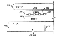
本発明の装置は、例えば5℃を超える正確な大きい温度差を達成することを探求するものであるが、例えば2W/cm2以下のように、大きいプラズマ熱流束を必要としないものである。図3Aは、本発明の一実施形態によるワーク温度制御装置を示す概略側面図である。ベース302すなわち熱交換器が断熱材304を支持している。該断熱材304上には、好ましくは平支持体306が取付けられている。支持体306内には、ヒータ308が埋設されている。支持体306上には、ウェーハのようなワーク310が配置されている。熱伝導体312が、支持体306とワーク310との間の熱的密接を形成している。熱伝導体312は、ヘリウムのようなガスが好ましい。ヘリウム圧力は、ワーク310と支持体306との熱伝導を制御する。
The apparatus of the present invention seeks to achieve an accurate large temperature difference, for example exceeding 5 ° C., but does not require a large plasma heat flux, for example 2 W / cm 2 or less. FIG. 3A is a schematic side view showing a workpiece temperature control apparatus according to an embodiment of the present invention. A base 302 or heat exchanger supports the
一実施形態によれば、ベース302は、冷却/加熱流体ループのような慣用の熱交換システムを通して比較的一定温度に維持される金属材料(好ましくはアルミニウムベースの冷却板)で構成される。他の実施形態によれば、ベース302は、窒化アルミニウムのような非金属材料で構成することもできる。しかしながら、ベース302は、ヒータ308を用いない標準的作動時におけるよりも大きく冷却されなければならない。例えば、ベース302の温度は、ワーク310の所望温度よりも10〜50℃低くすることができる。ベース302はまた、プラズマ加熱の場合の熱シンクを形成する。ベースプレート302の温度を維持するため、外部クーラント冷却器(図示せず)を使用することもできる。外部クーラント冷却器により除去される熱量およびクーラントの温度は、それぞれ、2000Wおよび−20℃以下に制限できる。ベース302には、ヒータ用給電線312または他のサービスラインを配置するための幾つかの孔およびキャビティ(図示せず)を設けることができる。このようなサービスラインとして、ヒータ、センサ、高電圧静電クランプ用の給電線がある。当業者ならば、サービスラインは前掲のものに限定されないことは理解されよう。
According to one embodiment, the
一実施形態によれば、断熱材304は、支持体306とベース302との間の大きい熱インピーダンス断熱層(thermal impedance break)として機能する。断熱材304は、ポリマー、プラスチックまたはセラミックで作られた厚いRTV接着層で構成できる。しかしながら、断熱材304の熱インピーダンス断熱層は、ウェーハ310の冷却が不充分になるほど過度のものであってはならない。例えば、断熱材は、約0.05〜0.20W/mKの範囲の熱伝導率を有するのが好ましい。この場合、断熱材304は、耐熱要素として、および支持体306とベース302との接合材としての両機能を有する。また、断熱材304は、プラズマとベース304との間に充分なRFカップリングが維持されるものでなくてはならない。また、断熱材304は、層の上下に存在する異なる材料および温度による大きい熱−機械的剪断を許容できなくてはならない。一実施形態によれば、断熱材304の厚さは2mm以下にすべきである。断熱材304には、ヒータ用給電線312および他のサービスラインを収容するための、ベース304のキャビティに隣接する幾つかのキャビティまたはバイア(vias)(図示せず)を設けることができる。
According to one embodiment, the
一実施形態によれば、支持体306はセラミック材料で構成される。セラミックは、例えばアルミナのような非導電性材料で形成できる。支持体306の形状は、プラズマエッチングシステムに一般的に使用されている慣用ディスクにするのが好ましい。ワーク306は慣用の静電チャックで構成するか、ウェーハ310を保持する機械的クランプを備えたセラミックで構成できる。一実施形態によれば、支持体306の厚さは約2mmである。しかしながら、当業者ならば、他の厚さも適していることは理解されよう。他の実施形態によれば、支持体306の構造は「ベースに接合された薄いディスク」であり、そうでなければ、側方熱伝導が非常に高くなり、ヒータ入力が側方に拡大されてゾーン分離が非効率的になってしまう。支持体は、熱を局部的に散逸させることができる。
According to one embodiment, the
ヒータ308は、少なくとも1つの抵抗要素を有している。一実施形態によれば、ヒータ308は、クランプ電極平面の下で支持体306内に埋設でき、かつ例えば対称的または任意の所望パターンの形状にすることができる。ヒータ308は、1以上の平加熱要素で構成することもできる。各加熱要素は、独立的に制御される加熱ゾーンまたは領域を形成する。多ゾーンパターンは、支持体306への伝導冷却(conduction cooling)とは逆に作用する1以上の平加熱要素を有している。各加熱ゾーンに関連するセンサ309は、各加熱ゾーンの温度を測定しかつ信号をコントローラまたはコンピュータ(図7参照)に送って、個々の平加熱要素をモニタしかつ制御する。例えば、赤外線放射センサまたは熱電対センサ等のセンサは、ワーク310から直接読取りできるようにポートを通して取付けることができる。センサ309は支持体306内または背面に取付けることもできる。ヒータ308には、断熱材304およびベース302の開口を通って配置される給電線312により給電できる。
The
一実施形態によれば、ヒータ308は誘導ヒータで構成される。他の実施形態によれば、ヒータ308は、クリプトンランプまたは石英ランプ等の加熱ランプで構成される。更に別の実施形態によれば、ヒータ308は、冷却または加熱が可能な熱電モジュールで構成できる。熱電モジュールを用いる場合には、ベースまたは断熱層は任意に構成できる。当業者ならば、支持体306を加熱するのに他の多くの方法があることは理解されよう。
According to one embodiment, the
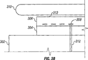
図3Bには、本発明の他の実施形態が示されている。図3Bの実施形態では、ヒータ308は、薄膜ヒータのような蝕刻箔技術で形成される。ヒータ308はワーク支持体306内に埋設するか、ワーク支持体306の背面上に取付けることができる(図示せず)。断熱材304と支持体306との間および断熱材304とベース302との間には、ポリマーのような接合層(図示せず。各層の厚さは例えば0.003インチである)が配置される。
FIG. 3B shows another embodiment of the present invention. In the embodiment of FIG. 3B, the
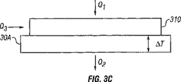
図3Cは、図3Aの装置における熱流量力学を示す簡単化された概略図である。進入するプラズマ熱流束Q1は、ウェーハ310の表面上の温度T1に寄与する。ヒータ308は、ウェーハ310に熱Q3を供給する。ワーク支持体306を通り冷却されたベース302に入る、システムからの外出熱流束Q2は、進入熱流束Q1およびQ3の合計にほぼ等しく、従って次式のように表される。
Q1+Q3=Q2
定義により、ウェーハ310の温度T1と、断熱材304を通る温度ΔTとの合計は、冷却されたベース302の温度T1に等しい。
T1=T2+ΔT
ΔTは、断熱材304の熱伝導率により定められることに留意されたい。かくして、ヒータ308により発生される進入熱流束Q3はΔTを制御する。従って、ヒータ308の出力は、Q1の範囲でウェーハの表面上に所望温度T1が得られるように調節される。
FIG. 3C is a simplified schematic diagram illustrating thermal flow dynamics in the apparatus of FIG. 3A. The incoming plasma heat flux Q1 contributes to the temperature T1 on the surface of the
Q1 + Q3 = Q2
By definition, the sum of the temperature T 1 of the
T1 = T2 + ΔT
Note that ΔT is determined by the thermal conductivity of the
好ましくは、ベース302の温度は、進入熱流束Q1が存在せず、かつ最大熱流束Q3が最大熱流束Q1にほぼ等しいとき、最大進入熱流束Q3の約1/2の外出熱流束Q2を発生するように設定される。すなわち、
Q1=0でありかつQ3max≒Q1maxであるとき、
Q2≒1/2・Q3max
Preferably, the temperature of the
When Q1 = 0 and Q3 max ≈Q1 max ,
Q2 ≒ 1/2 ・ Q3 max
この好ましいスキームでは、T1が変化できる範囲は最大化される。すなわち、ウェーハの局部的温度は、ヒータ308のゾーンの加熱出力を制御することにより調節できる。一実施形態によれば、ベース302の温度すなわちクーラント温度は、最大値Q1と最大値Q3との合計が最大値Q2に等しくなる慣用装置よりも約20℃低く設定される。
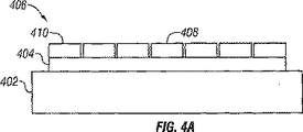
ここで図4Aの概略側面図を参照すると、ここには、本発明の他の実施形態に従ってワークの温度を制御する一体型単一平層電極/ヒータを備えた装置が示されている。ベース402は断熱材404を支持している。断熱材404上には平支持体406が取付けられている。一実施形態によれば、平支持体406は内側スパイラル408および外側スパイラル410を有し、これらの両スパイラル408、410は、ワークおよびワークをクランプする電極を加熱するヒータとして使用される。両ヒータおよび電極は、平支持体406により表される単一平層構造を形成するように一体化されている。図4Bは平支持体406の平面図である。内側スパイラル408と外側スパイラル410との間には差動高電圧HV412が印加され、平支持体406の静電クランプ機能を発生させる。差動高電圧HV412がアース(接地)に対して内側スパイラル408および外側スパイラル410の両者に印加される場合には、平支持体406は単極静電チャックとして機能する。差動高電圧HVが内側スパイラル408と外側スパイラル410との間に印加される場合には、平支持体406は双極チャックとして機能する。内側コイル408には第一制御電源414が接続され、第一加熱ゾーンを発生させる。外側コイル410には第二制御電源414が接続され、第二加熱ゾーンを発生させる。
In this preferred scheme, the range over which T1 can be varied is maximized. That is, the local temperature of the wafer can be adjusted by controlling the heating power of the
Referring now to the schematic side view of FIG. 4A, there is shown an apparatus with an integrated single flat layer electrode / heater that controls the temperature of the workpiece in accordance with another embodiment of the present invention. The
図5は、本発明の他の実施形態による側方断熱層(lateral thermal break)アプローチを用いたワーク温度制御装置を示す概略側面図である。直接電気加熱または異なる温度のクーラントを用いる代わりに二重または多重マニホルドヒートシンクを用いて、温度制御された流体を循環させることができる。温度制御されるベース502が、断熱材(例えばセラミック)504を支持する。平支持体506がワーク508の支持体を形成する。ベース502は、断熱材510により、2以上のゾーンに方位角的に分離されており、各ゾーンがヒートシンクを表している。矢印は異なるヒートシンクゾーンを表している。より詳しくは、側方断熱層510が、ヒートシンクを2以上のサーマルゾーン、例えばゾーンT1、T2に分離している。各サーマルゾーンの温度は、各流体ループ内の流体温度を制御することにより独立的に制御できる。このような断熱層510の使用により、任意の空間ゾーンを考慮に入れることができる。
FIG. 5 is a schematic side view illustrating a workpiece temperature control apparatus using a lateral thermal break approach according to another embodiment of the present invention. Instead of using direct electrical heating or different temperature coolants, dual or multiple manifold heat sinks can be used to circulate the temperature controlled fluid. A temperature controlled
図6は、本発明の一実施形態によるチャックの温度を制御する方法を示すフローチャートである。より詳しくは、図6は、2つの別個のサーマルゾーンを備えたチャックの温度制御方法を示すものである。当業者ならば、本発明の方法が1以上のサーマルゾーンを有するチャックに適用できることが理解されよう。第一ブロック602では、第一組のセンサを用いて第一ゾーンの温度が測定される。これらの測定値に基いて、ブロック604では、第一ゾーンの温度に影響を与える加熱要素の出力を制御して、第一ゾーンの温度を、ユーザおよび/またはコンピュータにより設定された温度に調節する。第二ブロック606では、第二組のセンサを用いて第二ゾーンの温度が測定される。これらの測定値に基いて、ブロック608では、第二ゾーンの温度に影響を与える加熱要素の出力を制御して、第二ゾーンの温度を、ユーザおよび/またはコンピュータにより設定された温度に調節する。
FIG. 6 is a flowchart illustrating a method for controlling the temperature of a chuck according to an embodiment of the present invention. More specifically, FIG. 6 shows a temperature control method for a chuck with two separate thermal zones. One skilled in the art will appreciate that the method of the present invention is applicable to chucks having one or more thermal zones. In a
図7は、本発明の一実施形態によるチャックの温度制御システムを示す概略図である。ユーザ702はコンピュータ704に1組のパラメータを入力する。このようなパラメータの組として、例えば、チャックの第一ゾーンの所望温度およびチャックの第二ゾーンの所望温度がある。当業者ならば、チャックに1以上のゾーンを設けることができることは理解されよう。コンピュータ704は、図6のアルゴリズム、コンピュータ704の入力および出力を記憶している記憶要素706と通信する。第一組のセンサ708がチャックの第一ゾーンを測定し、第2組のセンサ710がチャックの第二ゾーンを測定する。第一組のセンサ708の温度測定値に基いて、コンピュータ704は、第一組の加熱要素712を制御してチャックの第一ゾーンの温度を調節する。第二組のセンサ710の温度測定値に基いて、コンピュータ704は、第二組の加熱要素714を制御してチャックの第二ゾーンの温度を調節する。
FIG. 7 is a schematic diagram illustrating a chuck temperature control system according to an embodiment of the present invention.
静電チャック上のウェーハの温度分布を制御する上記方法は、誘導結合プラズマ(Inductive Coupled Plasma:ICP)加工機での適用に適しているだけでなく、特に、ウェーハへの低プラズマ出力熱流束を必要とする他の任意のシステムへの用途にも適している。この技術は、本発明の技術は、熱勾配を形成する必要性が存在する他の任意の用途に適用できる。 The above method for controlling the temperature distribution of the wafer on the electrostatic chuck is not only suitable for application in an inductive coupled plasma (ICP) processing machine, but in particular a low plasma output heat flux to the wafer. It is also suitable for use in any other system that requires it. This technique can be applied to any other application where there is a need for the technique of the present invention to form a thermal gradient.
以上、本発明の実施形態および用途を図示しかつ説明したが、本願開示の利益を有する当業者ならば、本発明の概念から逸脱することなく、上記以外の多くの変更形態を想到し得ることは明白である。従って本発明は、特許請求の範囲に記載の精神を除き、いかなる制限を受けるものではない。 While the embodiments and applications of the present invention have been illustrated and described, those skilled in the art having the benefit of this disclosure may conceive many other variations without departing from the concept of the present invention. Is obvious. Accordingly, the invention is not limited in any way except by the spirit described in the claims.
302 ベース
304 断熱材
306 支持体
308ヒータ
310 ワーク(ウェーハ)
412 差動高電圧
414 第一ヒータ電源
416 第二ヒータ電源
302
412 Differential high voltage 414 1st heater power supply 416 2nd heater power supply
Claims (22)
該ベース上に配置される断熱材の層と、を有し、前記断熱材は、0.05W/mKから0.20W/mKの範囲の熱伝導率を有し、
ワークを支持する静電チャックを更に有し、前記チャックは、前記断熱材の層の上に配置され、前記チャックは、前記断熱材の層によって前記ベースに結合され、処理中にプラズマから進入する熱流束を受け入れ、
前記静電チャック内に埋設されたヒータを更に有し、前記ヒータおよび前記静電チャックは、単一の平らな層を形成することを特徴とする支持体。A temperature controlled base having a temperature below the desired temperature of the workpiece;
A layer of thermal insulation disposed on the base, the thermal insulation having a thermal conductivity in the range of 0.05 W / mK to 0.20 W / mK;
An electrostatic chuck for supporting a workpiece is further provided, the chuck being disposed on the layer of insulation, the chuck being coupled to the base by the layer of insulation and entering from the plasma during processing. Accept heat flux,
The support further comprising a heater embedded in the electrostatic chuck, wherein the heater and the electrostatic chuck form a single flat layer.
ワークを支持体の頂面に当接させて保持する段階を有し、前記支持体は、
ワークの所望温度以下の温度を有する温度制御型ベースと、
該ベース上に配置される断熱材の層と、を有し、前記断熱材は、0.05W/mKから0.20W/mKの範囲の熱伝導率を有し、
ワークを支持する静電チャックを更に有し、前記チャックは、前記断熱材の層の上
に配置され、前記チャックは、前記断熱材の層によって前記ベースに結合され、処理
中にプラズマから入って来る熱流束を受け入れ、
前記静電チャック内に埋設されたヒータを更に有し、前記ヒータおよび前記静電チャックは、単一の平らな層を形成し、
前記ワークを横切る温度を制御するために、それぞれの前記ヒータにより、ワークの各ゾーンを独立的に加熱する段階を更に有することを特徴とする、多ゾーンを有するワークを横切る温度制御方法。A temperature control method across a workpiece having multiple zones, the method comprising:
And holding the work in contact with the top surface of the support,
A temperature controlled base having a temperature below the desired temperature of the workpiece;
A layer of thermal insulation disposed on the base, the thermal insulation having a thermal conductivity in the range of 0.05 W / mK to 0.20 W / mK;
An electrostatic chuck for supporting a workpiece, the chuck being disposed on the layer of insulation, the chuck being coupled to the base by the layer of insulation and entering from the plasma during processing; Accept the incoming heat flux,
Further comprising a heater embedded in the electrostatic chuck, the heater and the electrostatic chuck forming a single flat layer;
The method of controlling temperature across a workpiece having multiple zones, further comprising the step of independently heating each zone of the workpiece by each of the heaters in order to control the temperature across the workpiece.
Applications Claiming Priority (3)
| Application Number | Priority Date | Filing Date | Title |
|---|---|---|---|
| US84643201A | 2001-04-30 | 2001-04-30 | |
| US10/062,395 US6847014B1 (en) | 2001-04-30 | 2002-02-01 | Method and apparatus for controlling the spatial temperature distribution across the surface of a workpiece support |
| PCT/US2002/012864 WO2002089531A1 (en) | 2001-04-30 | 2002-04-23 | Method and apparatus for controlling the spatial temperature distribution across the surface of a workpiece support |
Related Child Applications (1)
| Application Number | Title | Priority Date | Filing Date |
|---|---|---|---|
| JP2009136934A Division JP5388704B2 (en) | 2001-04-30 | 2009-06-08 | Method and apparatus for controlling spatial temperature distribution across the surface of a workpiece support |
Publications (3)
| Publication Number | Publication Date |
|---|---|
| JP2004533718A JP2004533718A (en) | 2004-11-04 |
| JP2004533718A5 JP2004533718A5 (en) | 2005-12-22 |
| JP4549022B2 true JP4549022B2 (en) | 2010-09-22 |
Family
ID=26742208
Family Applications (1)
| Application Number | Title | Priority Date | Filing Date |
|---|---|---|---|
| JP2002586683A Expired - Lifetime JP4549022B2 (en) | 2001-04-30 | 2002-04-23 | Method and apparatus for controlling spatial temperature distribution across the surface of a workpiece support |
Country Status (6)
| Country | Link |
|---|---|
| US (3) | US8536494B2 (en) |
| EP (1) | EP1391140B1 (en) |
| JP (1) | JP4549022B2 (en) |
| CN (1) | CN100401852C (en) |
| TW (1) | TWI267160B (en) |
| WO (1) | WO2002089531A1 (en) |
Families Citing this family (151)
| Publication number | Priority date | Publication date | Assignee | Title |
|---|---|---|---|---|
| JP4549022B2 (en) | 2001-04-30 | 2010-09-22 | ラム リサーチ コーポレイション | Method and apparatus for controlling spatial temperature distribution across the surface of a workpiece support |
| US20050211385A1 (en) * | 2001-04-30 | 2005-09-29 | Lam Research Corporation, A Delaware Corporation | Method and apparatus for controlling spatial temperature distribution |
| US7347901B2 (en) | 2002-11-29 | 2008-03-25 | Tokyo Electron Limited | Thermally zoned substrate holder assembly |
| US7230204B2 (en) | 2003-03-28 | 2007-06-12 | Tokyo Electron Limited | Method and system for temperature control of a substrate |
| US20040222210A1 (en) * | 2003-05-08 | 2004-11-11 | Hongy Lin | Multi-zone ceramic heating system and method of manufacture thereof |
| JP4686996B2 (en) * | 2004-03-30 | 2011-05-25 | 住友電気工業株式会社 | Heating device |
| US7731798B2 (en) * | 2004-12-01 | 2010-06-08 | Ultratech, Inc. | Heated chuck for laser thermal processing |
| US8038796B2 (en) | 2004-12-30 | 2011-10-18 | Lam Research Corporation | Apparatus for spatial and temporal control of temperature on a substrate |
| JP4672597B2 (en) * | 2005-06-02 | 2011-04-20 | 日本碍子株式会社 | Substrate processing equipment |
| US7525787B2 (en) * | 2005-09-30 | 2009-04-28 | Lam Research Corporation | Electrostatic chuck assembly with dielectric material and/or cavity having varying thickness, profile and/or shape, method of use and apparatus incorporating same |
| US7956310B2 (en) * | 2005-09-30 | 2011-06-07 | Tokyo Electron Limited | Stage, substrate processing apparatus, plasma processing apparatus, control method for stage, control method for plasma processing apparatus, and storage media |
| US7297894B1 (en) | 2006-09-25 | 2007-11-20 | Tokyo Electron Limited | Method for multi-step temperature control of a substrate |
| US7723648B2 (en) * | 2006-09-25 | 2010-05-25 | Tokyo Electron Limited | Temperature controlled substrate holder with non-uniform insulation layer for a substrate processing system |
| US7838800B2 (en) | 2006-09-25 | 2010-11-23 | Tokyo Electron Limited | Temperature controlled substrate holder having erosion resistant insulating layer for a substrate processing system |
| JP5203612B2 (en) * | 2007-01-17 | 2013-06-05 | 株式会社日立ハイテクノロジーズ | Plasma processing equipment |
| US8673080B2 (en) | 2007-10-16 | 2014-03-18 | Novellus Systems, Inc. | Temperature controlled showerhead |
| JP5414172B2 (en) | 2007-12-05 | 2014-02-12 | 株式会社日立ハイテクノロジーズ | Plasma processing apparatus and plasma processing method |
| JP5171584B2 (en) * | 2008-03-26 | 2013-03-27 | 株式会社日立国際電気 | Substrate mounting table for substrate processing apparatus, substrate processing apparatus, and method for manufacturing semiconductor device |
| US20100116788A1 (en) * | 2008-11-12 | 2010-05-13 | Lam Research Corporation | Substrate temperature control by using liquid controlled multizone substrate support |
| JP5193886B2 (en) * | 2009-01-14 | 2013-05-08 | 株式会社巴川製紙所 | Electrostatic chuck device repair method and repair device, and electrostatic chuck device |
| KR101691044B1 (en) * | 2009-02-04 | 2016-12-29 | 맷슨 테크놀로지, 인크. | Electrostatic chuck system and process for radially tuning the temperature profile across the surface of a substrate |
| US8637794B2 (en) | 2009-10-21 | 2014-01-28 | Lam Research Corporation | Heating plate with planar heating zones for semiconductor processing |
| KR101841378B1 (en) * | 2009-12-15 | 2018-03-22 | 램 리써치 코포레이션 | Adjusting substrate temperature to improve cd uniformity |
| US9034142B2 (en) | 2009-12-18 | 2015-05-19 | Novellus Systems, Inc. | Temperature controlled showerhead for high temperature operations |
| JP5423632B2 (en) * | 2010-01-29 | 2014-02-19 | 住友大阪セメント株式会社 | Electrostatic chuck device |
| EP2383771B1 (en) * | 2010-04-29 | 2020-04-22 | EV Group GmbH | Method and device for loosening a polymer coating from a surface of a substrate |
| US8410393B2 (en) | 2010-05-24 | 2013-04-02 | Lam Research Corporation | Apparatus and method for temperature control of a semiconductor substrate support |
| US8791392B2 (en) | 2010-10-22 | 2014-07-29 | Lam Research Corporation | Methods of fault detection for multiplexed heater array |
| US8546732B2 (en) | 2010-11-10 | 2013-10-01 | Lam Research Corporation | Heating plate with planar heater zones for semiconductor processing |
| US10283321B2 (en) | 2011-01-18 | 2019-05-07 | Applied Materials, Inc. | Semiconductor processing system and methods using capacitively coupled plasma |
| KR101937115B1 (en) | 2011-03-04 | 2019-01-09 | 노벨러스 시스템즈, 인코포레이티드 | Hybrid ceramic showerhead |
| US8552346B2 (en) * | 2011-05-20 | 2013-10-08 | Applied Materials, Inc. | Methods and apparatus for controlling temperature of a multi-zone heater in an process chamber |
| US9307578B2 (en) | 2011-08-17 | 2016-04-05 | Lam Research Corporation | System and method for monitoring temperatures of and controlling multiplexed heater array |
| US10388493B2 (en) | 2011-09-16 | 2019-08-20 | Lam Research Corporation | Component of a substrate support assembly producing localized magnetic fields |
| US8624168B2 (en) | 2011-09-20 | 2014-01-07 | Lam Research Corporation | Heating plate with diode planar heater zones for semiconductor processing |
| US8461674B2 (en) | 2011-09-21 | 2013-06-11 | Lam Research Corporation | Thermal plate with planar thermal zones for semiconductor processing |
| US9869392B2 (en) | 2011-10-20 | 2018-01-16 | Lam Research Corporation | Edge seal for lower electrode assembly |
| US9859142B2 (en) | 2011-10-20 | 2018-01-02 | Lam Research Corporation | Edge seal for lower electrode assembly |
| US9324589B2 (en) | 2012-02-28 | 2016-04-26 | Lam Research Corporation | Multiplexed heater array using AC drive for semiconductor processing |
| US9960059B2 (en) * | 2012-03-30 | 2018-05-01 | Taiwan Semiconductor Manufacturing Company, Ltd. | Honeycomb heaters for integrated circuit manufacturing |
| US8677586B2 (en) | 2012-04-04 | 2014-03-25 | Lam Research Corporation | Installation fixture for elastomer bands and methods of using the same |
| US8809747B2 (en) | 2012-04-13 | 2014-08-19 | Lam Research Corporation | Current peak spreading schemes for multiplexed heated array |
| US8937800B2 (en) * | 2012-04-24 | 2015-01-20 | Applied Materials, Inc. | Electrostatic chuck with advanced RF and temperature uniformity |
| US9132436B2 (en) | 2012-09-21 | 2015-09-15 | Applied Materials, Inc. | Chemical control features in wafer process equipment |
| US10049948B2 (en) | 2012-11-30 | 2018-08-14 | Lam Research Corporation | Power switching system for ESC with array of thermal control elements |
| JP5992388B2 (en) * | 2012-12-03 | 2016-09-14 | 日本碍子株式会社 | Ceramic heater |
| US10177014B2 (en) | 2012-12-14 | 2019-01-08 | Applied Materials, Inc. | Thermal radiation barrier for substrate processing chamber components |
| US10256079B2 (en) | 2013-02-08 | 2019-04-09 | Applied Materials, Inc. | Semiconductor processing systems having multiple plasma configurations |
| US10085585B2 (en) * | 2013-02-21 | 2018-10-02 | Rain Mountain, Llc | System and methods of improving the performance, safety and energy efficiency of a cooking appliance |
| US9677772B2 (en) | 2013-02-21 | 2017-06-13 | Rain Mountain, Llc | Intelligent ventilating safety range hood control system |
| US9362130B2 (en) | 2013-03-01 | 2016-06-07 | Applied Materials, Inc. | Enhanced etching processes using remote plasma sources |
| US20140251214A1 (en) * | 2013-03-06 | 2014-09-11 | Applied Materials, Inc. | Heated substrate support with flatness control |
| CN104112638B (en) * | 2013-04-22 | 2017-07-18 | 中微半导体设备(上海)有限公司 | A kind of plasma-reaction-chamber and its electrostatic chuck |
| US9502279B2 (en) | 2013-06-28 | 2016-11-22 | Lam Research Corporation | Installation fixture having a micro-grooved non-stick surface |
| DE102014202302B4 (en) * | 2013-07-03 | 2015-02-19 | Technische Universität Dresden | Device for heating preforms |
| CN105340073A (en) * | 2013-07-04 | 2016-02-17 | Ev集团E·索尔纳有限责任公司 | Method and device for treating a substrate surface |
| CN104637838B (en) * | 2013-11-15 | 2018-06-26 | 中微半导体设备(上海)有限公司 | A kind of semiconductor processing device |
| US10217615B2 (en) | 2013-12-16 | 2019-02-26 | Lam Research Corporation | Plasma processing apparatus and component thereof including an optical fiber for determining a temperature thereof |
| US9583377B2 (en) | 2013-12-17 | 2017-02-28 | Lam Research Corporation | Installation fixture for elastomer bands |
| US9101038B2 (en) | 2013-12-20 | 2015-08-04 | Lam Research Corporation | Electrostatic chuck including declamping electrode and method of declamping |
| US10090211B2 (en) | 2013-12-26 | 2018-10-02 | Lam Research Corporation | Edge seal for lower electrode assembly |
| JP6240532B2 (en) * | 2014-02-27 | 2017-11-29 | 東京エレクトロン株式会社 | Electrostatic chuck temperature control method |
| US10741365B2 (en) | 2014-05-05 | 2020-08-11 | Lam Research Corporation | Low volume showerhead with porous baffle |
| US9309598B2 (en) | 2014-05-28 | 2016-04-12 | Applied Materials, Inc. | Oxide and metal removal |
| JP6265841B2 (en) | 2014-06-11 | 2018-01-24 | 東京エレクトロン株式会社 | Plasma processing apparatus and method of operating plasma processing apparatus |
| US9966240B2 (en) | 2014-10-14 | 2018-05-08 | Applied Materials, Inc. | Systems and methods for internal surface conditioning assessment in plasma processing equipment |
| US9355922B2 (en) | 2014-10-14 | 2016-05-31 | Applied Materials, Inc. | Systems and methods for internal surface conditioning in plasma processing equipment |
| US10002782B2 (en) | 2014-10-17 | 2018-06-19 | Lam Research Corporation | ESC assembly including an electrically conductive gasket for uniform RF power delivery therethrough |
| US11637002B2 (en) | 2014-11-26 | 2023-04-25 | Applied Materials, Inc. | Methods and systems to enhance process uniformity |
| US10224210B2 (en) | 2014-12-09 | 2019-03-05 | Applied Materials, Inc. | Plasma processing system with direct outlet toroidal plasma source |
| US10573496B2 (en) | 2014-12-09 | 2020-02-25 | Applied Materials, Inc. | Direct outlet toroidal plasma source |
| US11257693B2 (en) | 2015-01-09 | 2022-02-22 | Applied Materials, Inc. | Methods and systems to improve pedestal temperature control |
| US9728437B2 (en) | 2015-02-03 | 2017-08-08 | Applied Materials, Inc. | High temperature chuck for plasma processing systems |
| US10378107B2 (en) | 2015-05-22 | 2019-08-13 | Lam Research Corporation | Low volume showerhead with faceplate holes for improved flow uniformity |
| US10023959B2 (en) | 2015-05-26 | 2018-07-17 | Lam Research Corporation | Anti-transient showerhead |
| US10763142B2 (en) | 2015-06-22 | 2020-09-01 | Lam Research Corporation | System and method for determining field non-uniformities of a wafer processing chamber using a wafer processing parameter |
| US10381248B2 (en) | 2015-06-22 | 2019-08-13 | Lam Research Corporation | Auto-correction of electrostatic chuck temperature non-uniformity |
| US10386821B2 (en) * | 2015-06-22 | 2019-08-20 | Lam Research Corporation | Systems and methods for calibrating scalar field contribution values for a limited number of sensors including a temperature value of an electrostatic chuck and estimating temperature distribution profiles based on calibrated values |
| US9691645B2 (en) * | 2015-08-06 | 2017-06-27 | Applied Materials, Inc. | Bolted wafer chuck thermal management systems and methods for wafer processing systems |
| US9741593B2 (en) | 2015-08-06 | 2017-08-22 | Applied Materials, Inc. | Thermal management systems and methods for wafer processing systems |
| US9349605B1 (en) | 2015-08-07 | 2016-05-24 | Applied Materials, Inc. | Oxide etch selectivity systems and methods |
| US10504700B2 (en) | 2015-08-27 | 2019-12-10 | Applied Materials, Inc. | Plasma etching systems and methods with secondary plasma injection |
| KR20190126450A (en) * | 2015-10-06 | 2019-11-11 | 에이에스엠엘 홀딩 엔.브이. | Chucks and clamps for holding objects of a lithographic apparatus and methods for controlling a temperature of an object held by a clamp of a lithographic apparatus |
| US10154542B2 (en) | 2015-10-19 | 2018-12-11 | Watlow Electric Manufacturing Company | Composite device with cylindrical anisotropic thermal conductivity |
| CN106935468A (en) * | 2015-12-31 | 2017-07-07 | 中微半导体设备(上海)有限公司 | A kind of semiconductor processor and the multi-region temp controlling heater for semiconductor processor |
| US10582570B2 (en) | 2016-01-22 | 2020-03-03 | Applied Materials, Inc. | Sensor system for multi-zone electrostatic chuck |
| US10504754B2 (en) | 2016-05-19 | 2019-12-10 | Applied Materials, Inc. | Systems and methods for improved semiconductor etching and component protection |
| US10522371B2 (en) | 2016-05-19 | 2019-12-31 | Applied Materials, Inc. | Systems and methods for improved semiconductor etching and component protection |
| US11069553B2 (en) * | 2016-07-07 | 2021-07-20 | Lam Research Corporation | Electrostatic chuck with features for preventing electrical arcing and light-up and improving process uniformity |
| US10629473B2 (en) | 2016-09-09 | 2020-04-21 | Applied Materials, Inc. | Footing removal for nitride spacer |
| JP6767833B2 (en) * | 2016-09-29 | 2020-10-14 | 日本特殊陶業株式会社 | Heating device |
| US10546729B2 (en) | 2016-10-04 | 2020-01-28 | Applied Materials, Inc. | Dual-channel showerhead with improved profile |
| US9934942B1 (en) | 2016-10-04 | 2018-04-03 | Applied Materials, Inc. | Chamber with flow-through source |
| US10062579B2 (en) | 2016-10-07 | 2018-08-28 | Applied Materials, Inc. | Selective SiN lateral recess |
| US10163696B2 (en) | 2016-11-11 | 2018-12-25 | Applied Materials, Inc. | Selective cobalt removal for bottom up gapfill |
| US9768034B1 (en) | 2016-11-11 | 2017-09-19 | Applied Materials, Inc. | Removal methods for high aspect ratio structures |
| US10026621B2 (en) | 2016-11-14 | 2018-07-17 | Applied Materials, Inc. | SiN spacer profile patterning |
| US10242908B2 (en) | 2016-11-14 | 2019-03-26 | Applied Materials, Inc. | Airgap formation with damage-free copper |
| US10566206B2 (en) | 2016-12-27 | 2020-02-18 | Applied Materials, Inc. | Systems and methods for anisotropic material breakthrough |
| US10910195B2 (en) | 2017-01-05 | 2021-02-02 | Lam Research Corporation | Substrate support with improved process uniformity |
| US10403507B2 (en) | 2017-02-03 | 2019-09-03 | Applied Materials, Inc. | Shaped etch profile with oxidation |
| US10431429B2 (en) | 2017-02-03 | 2019-10-01 | Applied Materials, Inc. | Systems and methods for radial and azimuthal control of plasma uniformity |
| US10319739B2 (en) | 2017-02-08 | 2019-06-11 | Applied Materials, Inc. | Accommodating imperfectly aligned memory holes |
| US10943834B2 (en) | 2017-03-13 | 2021-03-09 | Applied Materials, Inc. | Replacement contact process |
| US10319649B2 (en) | 2017-04-11 | 2019-06-11 | Applied Materials, Inc. | Optical emission spectroscopy (OES) for remote plasma monitoring |
| US11276590B2 (en) | 2017-05-17 | 2022-03-15 | Applied Materials, Inc. | Multi-zone semiconductor substrate supports |
| US11276559B2 (en) | 2017-05-17 | 2022-03-15 | Applied Materials, Inc. | Semiconductor processing chamber for multiple precursor flow |
| US10497579B2 (en) | 2017-05-31 | 2019-12-03 | Applied Materials, Inc. | Water-free etching methods |
| US10920320B2 (en) | 2017-06-16 | 2021-02-16 | Applied Materials, Inc. | Plasma health determination in semiconductor substrate processing reactors |
| US10541246B2 (en) | 2017-06-26 | 2020-01-21 | Applied Materials, Inc. | 3D flash memory cells which discourage cross-cell electrical tunneling |
| US10727080B2 (en) | 2017-07-07 | 2020-07-28 | Applied Materials, Inc. | Tantalum-containing material removal |
| US10541184B2 (en) | 2017-07-11 | 2020-01-21 | Applied Materials, Inc. | Optical emission spectroscopic techniques for monitoring etching |
| US10354889B2 (en) | 2017-07-17 | 2019-07-16 | Applied Materials, Inc. | Non-halogen etching of silicon-containing materials |
| US10170336B1 (en) | 2017-08-04 | 2019-01-01 | Applied Materials, Inc. | Methods for anisotropic control of selective silicon removal |
| US10043674B1 (en) | 2017-08-04 | 2018-08-07 | Applied Materials, Inc. | Germanium etching systems and methods |
| US10297458B2 (en) | 2017-08-07 | 2019-05-21 | Applied Materials, Inc. | Process window widening using coated parts in plasma etch processes |
| JP6392961B2 (en) * | 2017-09-13 | 2018-09-19 | 日本特殊陶業株式会社 | Electrostatic chuck |
| US10424487B2 (en) | 2017-10-24 | 2019-09-24 | Applied Materials, Inc. | Atomic layer etching processes |
| US10128086B1 (en) | 2017-10-24 | 2018-11-13 | Applied Materials, Inc. | Silicon pretreatment for nitride removal |
| US10283324B1 (en) | 2017-10-24 | 2019-05-07 | Applied Materials, Inc. | Oxygen treatment for nitride etching |
| US10256112B1 (en) | 2017-12-08 | 2019-04-09 | Applied Materials, Inc. | Selective tungsten removal |
| US10903054B2 (en) | 2017-12-19 | 2021-01-26 | Applied Materials, Inc. | Multi-zone gas distribution systems and methods |
| US11328909B2 (en) | 2017-12-22 | 2022-05-10 | Applied Materials, Inc. | Chamber conditioning and removal processes |
| US10854426B2 (en) | 2018-01-08 | 2020-12-01 | Applied Materials, Inc. | Metal recess for semiconductor structures |
| US10964512B2 (en) | 2018-02-15 | 2021-03-30 | Applied Materials, Inc. | Semiconductor processing chamber multistage mixing apparatus and methods |
| US10679870B2 (en) | 2018-02-15 | 2020-06-09 | Applied Materials, Inc. | Semiconductor processing chamber multistage mixing apparatus |
| TWI766433B (en) | 2018-02-28 | 2022-06-01 | 美商應用材料股份有限公司 | Systems and methods to form airgaps |
| US10593560B2 (en) | 2018-03-01 | 2020-03-17 | Applied Materials, Inc. | Magnetic induction plasma source for semiconductor processes and equipment |
| US10319600B1 (en) | 2018-03-12 | 2019-06-11 | Applied Materials, Inc. | Thermal silicon etch |
| US10497573B2 (en) | 2018-03-13 | 2019-12-03 | Applied Materials, Inc. | Selective atomic layer etching of semiconductor materials |
| US10573527B2 (en) | 2018-04-06 | 2020-02-25 | Applied Materials, Inc. | Gas-phase selective etching systems and methods |
| US10490406B2 (en) | 2018-04-10 | 2019-11-26 | Appled Materials, Inc. | Systems and methods for material breakthrough |
| US10699879B2 (en) | 2018-04-17 | 2020-06-30 | Applied Materials, Inc. | Two piece electrode assembly with gap for plasma control |
| US10886137B2 (en) | 2018-04-30 | 2021-01-05 | Applied Materials, Inc. | Selective nitride removal |
| US10872778B2 (en) | 2018-07-06 | 2020-12-22 | Applied Materials, Inc. | Systems and methods utilizing solid-phase etchants |
| US10755941B2 (en) | 2018-07-06 | 2020-08-25 | Applied Materials, Inc. | Self-limiting selective etching systems and methods |
| US10672642B2 (en) | 2018-07-24 | 2020-06-02 | Applied Materials, Inc. | Systems and methods for pedestal configuration |
| US11049755B2 (en) | 2018-09-14 | 2021-06-29 | Applied Materials, Inc. | Semiconductor substrate supports with embedded RF shield |
| US10892198B2 (en) | 2018-09-14 | 2021-01-12 | Applied Materials, Inc. | Systems and methods for improved performance in semiconductor processing |
| CN110911332B (en) * | 2018-09-14 | 2022-11-25 | 北京北方华创微电子装备有限公司 | Electrostatic chuck |
| US11062887B2 (en) | 2018-09-17 | 2021-07-13 | Applied Materials, Inc. | High temperature RF heater pedestals |
| US11417534B2 (en) | 2018-09-21 | 2022-08-16 | Applied Materials, Inc. | Selective material removal |
| US11682560B2 (en) | 2018-10-11 | 2023-06-20 | Applied Materials, Inc. | Systems and methods for hafnium-containing film removal |
| US11121002B2 (en) | 2018-10-24 | 2021-09-14 | Applied Materials, Inc. | Systems and methods for etching metals and metal derivatives |
| US11437242B2 (en) | 2018-11-27 | 2022-09-06 | Applied Materials, Inc. | Selective removal of silicon-containing materials |
| US11721527B2 (en) | 2019-01-07 | 2023-08-08 | Applied Materials, Inc. | Processing chamber mixing systems |
| US10920319B2 (en) | 2019-01-11 | 2021-02-16 | Applied Materials, Inc. | Ceramic showerheads with conductive electrodes |
| KR20210039825A (en) * | 2019-10-02 | 2021-04-12 | 삼성전자주식회사 | An apparatus for depositing a substrate and a deposition system having the same |
| US11551951B2 (en) | 2020-05-05 | 2023-01-10 | Applied Materials, Inc. | Methods and systems for temperature control for a substrate |
| US11688615B2 (en) * | 2020-08-19 | 2023-06-27 | Taiwan Semiconductor Manufacturing Co., Ltd. | System and method for heating semiconductor wafers |
| US20220415635A1 (en) * | 2021-06-25 | 2022-12-29 | Applied Materials, Inc. | Thermal management hardware for uniform temperature control for enhanced bake-out for cluster tool |
Family Cites Families (45)
| Publication number | Priority date | Publication date | Assignee | Title |
|---|---|---|---|---|
| US2152126A (en) * | 1936-10-02 | 1939-03-28 | John Wentworth | Heating device |
| US3634740A (en) * | 1970-04-20 | 1972-01-11 | Addressograph Multigraph | Electrostatic holddown |
| US4361749A (en) * | 1980-02-04 | 1982-11-30 | Western Electric Co., Inc. | Uniformly cooled plasma etching electrode |
| US4518848A (en) * | 1981-05-15 | 1985-05-21 | Gca Corporation | Apparatus for baking resist on semiconductor wafers |
| JPH079887B2 (en) * | 1985-05-22 | 1995-02-01 | 三洋電機株式会社 | Liquid phase epitaxial growth method |
| US5001594A (en) * | 1989-09-06 | 1991-03-19 | Mcnc | Electrostatic handling device |
| US5059770A (en) * | 1989-09-19 | 1991-10-22 | Watkins-Johnson Company | Multi-zone planar heater assembly and method of operation |
| CA2031912A1 (en) * | 1989-12-22 | 1991-06-23 | Robert Fred Pfost | Heated cover device |
| US5192849A (en) * | 1990-08-10 | 1993-03-09 | Texas Instruments Incorporated | Multipurpose low-thermal-mass chuck for semiconductor processing equipment |
| JP3238925B2 (en) * | 1990-11-17 | 2001-12-17 | 株式会社東芝 | Electrostatic chuck |
| JPH04196528A (en) | 1990-11-28 | 1992-07-16 | Toshiba Corp | Magnetron etching system |
| US5580607A (en) * | 1991-07-26 | 1996-12-03 | Tokyo Electron Limited | Coating apparatus and method |
| US5294778A (en) * | 1991-09-11 | 1994-03-15 | Lam Research Corporation | CVD platen heater system utilizing concentric electric heating elements |
| US5376213A (en) * | 1992-07-28 | 1994-12-27 | Tokyo Electron Limited | Plasma processing apparatus |
| JP2906006B2 (en) * | 1992-10-15 | 1999-06-14 | 東京エレクトロン株式会社 | Processing method and apparatus |
| US5413360A (en) * | 1992-12-01 | 1995-05-09 | Kyocera Corporation | Electrostatic chuck |
| US5460684A (en) * | 1992-12-04 | 1995-10-24 | Tokyo Electron Limited | Stage having electrostatic chuck and plasma processing apparatus using same |
| US5591269A (en) * | 1993-06-24 | 1997-01-07 | Tokyo Electron Limited | Vacuum processing apparatus |
| TW277139B (en) * | 1993-09-16 | 1996-06-01 | Hitachi Seisakusyo Kk | |
| US5529657A (en) * | 1993-10-04 | 1996-06-25 | Tokyo Electron Limited | Plasma processing apparatus |
| JP2647799B2 (en) * | 1994-02-04 | 1997-08-27 | 日本碍子株式会社 | Ceramic heater and manufacturing method thereof |
| JP3208029B2 (en) * | 1994-11-22 | 2001-09-10 | 株式会社巴川製紙所 | Electrostatic chuck device and manufacturing method thereof |
| US6133557A (en) * | 1995-01-31 | 2000-10-17 | Kyocera Corporation | Wafer holding member |
| US5854468A (en) * | 1996-01-25 | 1998-12-29 | Brooks Automation, Inc. | Substrate heating apparatus with cantilevered lifting arm |
| JP3537269B2 (en) * | 1996-05-21 | 2004-06-14 | アネルバ株式会社 | Multi-chamber sputtering equipment |
| WO1998005060A1 (en) * | 1996-07-31 | 1998-02-05 | The Board Of Trustees Of The Leland Stanford Junior University | Multizone bake/chill thermal cycling module |
| US6080215A (en) * | 1996-08-12 | 2000-06-27 | 3M Innovative Properties Company | Abrasive article and method of making such article |
| US5846375A (en) * | 1996-09-26 | 1998-12-08 | Micron Technology, Inc. | Area specific temperature control for electrode plates and chucks used in semiconductor processing equipment |
| US6022587A (en) * | 1997-05-13 | 2000-02-08 | Applied Materials, Inc. | Method and apparatus for improving film deposition uniformity on a substrate |
| US5978202A (en) * | 1997-06-27 | 1999-11-02 | Applied Materials, Inc. | Electrostatic chuck having a thermal transfer regulator pad |
| JP3318514B2 (en) * | 1997-08-06 | 2002-08-26 | 日本碍子株式会社 | Semiconductor support device |
| US6102909A (en) * | 1997-08-26 | 2000-08-15 | Ethicon, Inc. | Scissorlike electrosurgical cutting instrument |
| EP0915499B1 (en) * | 1997-11-05 | 2011-03-23 | Tokyo Electron Limited | Semiconductor wafer holding apparatus |
| JP3368461B2 (en) * | 1997-11-05 | 2003-01-20 | 東京エレクトロン株式会社 | shell |
| JP3400692B2 (en) * | 1997-11-05 | 2003-04-28 | 東京エレクトロン株式会社 | Wafer temperature control device and wafer storage room |
| JP3477062B2 (en) * | 1997-12-26 | 2003-12-10 | 京セラ株式会社 | Wafer heating device |
| US6020262A (en) | 1998-03-06 | 2000-02-01 | Siemens Aktiengesellschaft | Methods and apparatus for chemical mechanical planarization (CMP) of a semiconductor wafer |
| US6259592B1 (en) * | 1998-11-19 | 2001-07-10 | Applied Materials, Inc. | Apparatus for retaining a workpiece upon a workpiece support and method of manufacturing same |
| KR100593627B1 (en) * | 1999-02-16 | 2006-06-28 | 동경 엘렉트론 주식회사 | Processing apparatus, processing system, discrimination method and detection method |
| US6310755B1 (en) * | 1999-05-07 | 2001-10-30 | Applied Materials, Inc. | Electrostatic chuck having gas cavity and method |
| JP2001203257A (en) * | 2000-01-20 | 2001-07-27 | Sumitomo Electric Ind Ltd | Wafer holder for semiconductor manufacturing apparatus |
| US6472643B1 (en) | 2000-03-07 | 2002-10-29 | Silicon Valley Group, Inc. | Substrate thermal management system |
| US6847014B1 (en) * | 2001-04-30 | 2005-01-25 | Lam Research Corporation | Method and apparatus for controlling the spatial temperature distribution across the surface of a workpiece support |
| JP4549022B2 (en) | 2001-04-30 | 2010-09-22 | ラム リサーチ コーポレイション | Method and apparatus for controlling spatial temperature distribution across the surface of a workpiece support |
| US6770852B1 (en) | 2003-02-27 | 2004-08-03 | Lam Research Corporation | Critical dimension variation compensation across a wafer by means of local wafer temperature control |
-
2002
- 2002-04-23 JP JP2002586683A patent/JP4549022B2/en not_active Expired - Lifetime
- 2002-04-23 EP EP02723949A patent/EP1391140B1/en not_active Expired - Lifetime
- 2002-04-23 WO PCT/US2002/012864 patent/WO2002089531A1/en active Application Filing
- 2002-04-23 CN CNB028119460A patent/CN100401852C/en not_active Expired - Lifetime
- 2002-04-30 TW TW091108963A patent/TWI267160B/en not_active IP Right Cessation
-
2004
- 2004-11-30 US US11/001,219 patent/US8536494B2/en active Active
- 2004-11-30 US US11/001,218 patent/US7274004B2/en not_active Expired - Lifetime
-
2013
- 2013-08-13 US US13/965,719 patent/US8921740B2/en not_active Expired - Fee Related
Also Published As
| Publication number | Publication date |
|---|---|
| US8536494B2 (en) | 2013-09-17 |
| US7274004B2 (en) | 2007-09-25 |
| US20140034608A1 (en) | 2014-02-06 |
| US8921740B2 (en) | 2014-12-30 |
| EP1391140B1 (en) | 2012-10-10 |
| US20050173403A1 (en) | 2005-08-11 |
| CN100401852C (en) | 2008-07-09 |
| JP2004533718A (en) | 2004-11-04 |
| CN1529994A (en) | 2004-09-15 |
| TWI267160B (en) | 2006-11-21 |
| EP1391140A4 (en) | 2006-02-22 |
| EP1391140A1 (en) | 2004-02-25 |
| US20050173404A1 (en) | 2005-08-11 |
| WO2002089531A1 (en) | 2002-11-07 |
Similar Documents
| Publication | Publication Date | Title |
|---|---|---|
| JP4549022B2 (en) | Method and apparatus for controlling spatial temperature distribution across the surface of a workpiece support | |
| JP5388704B2 (en) | Method and apparatus for controlling spatial temperature distribution across the surface of a workpiece support | |
| KR101109440B1 (en) | Method and apparatus for controlling spatial temperature distribution | |
| US11302556B2 (en) | Apparatus for spatial and temporal control of temperature on a substrate | |
| KR102652012B1 (en) | Thermal management systems and methods for wafer processing systems |
Legal Events
| Date | Code | Title | Description |
|---|---|---|---|
| A521 | Request for written amendment filed |
Free format text: JAPANESE INTERMEDIATE CODE: A523 Effective date: 20050425 |
|
| A621 | Written request for application examination |
Free format text: JAPANESE INTERMEDIATE CODE: A621 Effective date: 20050425 |
|
| A131 | Notification of reasons for refusal |
Free format text: JAPANESE INTERMEDIATE CODE: A131 Effective date: 20081208 |
|
| A601 | Written request for extension of time |
Free format text: JAPANESE INTERMEDIATE CODE: A601 Effective date: 20090309 |
|
| A602 | Written permission of extension of time |
Free format text: JAPANESE INTERMEDIATE CODE: A602 Effective date: 20090316 |
|
| A521 | Request for written amendment filed |
Free format text: JAPANESE INTERMEDIATE CODE: A523 Effective date: 20090608 |
|
| A131 | Notification of reasons for refusal |
Free format text: JAPANESE INTERMEDIATE CODE: A131 Effective date: 20090914 |
|
| A521 | Request for written amendment filed |
Free format text: JAPANESE INTERMEDIATE CODE: A523 Effective date: 20091214 |
|
| A131 | Notification of reasons for refusal |
Free format text: JAPANESE INTERMEDIATE CODE: A131 Effective date: 20100308 |
|
| A521 | Request for written amendment filed |
Free format text: JAPANESE INTERMEDIATE CODE: A523 Effective date: 20100527 |
|
| TRDD | Decision of grant or rejection written | ||
| A01 | Written decision to grant a patent or to grant a registration (utility model) |
Free format text: JAPANESE INTERMEDIATE CODE: A01 Effective date: 20100621 |
|
| A01 | Written decision to grant a patent or to grant a registration (utility model) |
Free format text: JAPANESE INTERMEDIATE CODE: A01 |
|
| A61 | First payment of annual fees (during grant procedure) |
Free format text: JAPANESE INTERMEDIATE CODE: A61 Effective date: 20100706 |
|
| R150 | Certificate of patent or registration of utility model |
Ref document number: 4549022 Country of ref document: JP Free format text: JAPANESE INTERMEDIATE CODE: R150 Free format text: JAPANESE INTERMEDIATE CODE: R150 |
|
| FPAY | Renewal fee payment (event date is renewal date of database) |
Free format text: PAYMENT UNTIL: 20130716 Year of fee payment: 3 |
|
| R250 | Receipt of annual fees |
Free format text: JAPANESE INTERMEDIATE CODE: R250 |
|
| R250 | Receipt of annual fees |
Free format text: JAPANESE INTERMEDIATE CODE: R250 |
|
| R250 | Receipt of annual fees |
Free format text: JAPANESE INTERMEDIATE CODE: R250 |
|
| R250 | Receipt of annual fees |
Free format text: JAPANESE INTERMEDIATE CODE: R250 |
|
| R250 | Receipt of annual fees |
Free format text: JAPANESE INTERMEDIATE CODE: R250 |
|
| R250 | Receipt of annual fees |
Free format text: JAPANESE INTERMEDIATE CODE: R250 |
|
| R250 | Receipt of annual fees |
Free format text: JAPANESE INTERMEDIATE CODE: R250 |
|
| R250 | Receipt of annual fees |
Free format text: JAPANESE INTERMEDIATE CODE: R250 |
|
| R250 | Receipt of annual fees |
Free format text: JAPANESE INTERMEDIATE CODE: R250 |
|
| EXPY | Cancellation because of completion of term |