JP2009130665A - Piezoelectric oscillator - Google Patents
Piezoelectric oscillator Download PDFInfo
- Publication number
- JP2009130665A JP2009130665A JP2007304037A JP2007304037A JP2009130665A JP 2009130665 A JP2009130665 A JP 2009130665A JP 2007304037 A JP2007304037 A JP 2007304037A JP 2007304037 A JP2007304037 A JP 2007304037A JP 2009130665 A JP2009130665 A JP 2009130665A
- Authority
- JP
- Japan
- Prior art keywords
- piezoelectric
- semiconductor device
- package
- piezoelectric oscillator
- vibrating piece
- Prior art date
- Legal status (The legal status is an assumption and is not a legal conclusion. Google has not performed a legal analysis and makes no representation as to the accuracy of the status listed.)
- Withdrawn
Links
Images


Abstract
Description
本発明は、半導体装置に振動子のパッケージを接合して形成する圧電発振器の改良に関
する。
The present invention relates to an improvement in a piezoelectric oscillator formed by bonding a package of a vibrator to a semiconductor device.
HDD(ハード・ディスク・ドライブ)、モバイルコンピュータ、あるいはICカード
等の小型の情報機器や、携帯電話、自動車電話、またはページングシステム等の移動体通
信機器において、圧電振動子や圧電発振器が広く使用されている。
圧電発振器は、圧電材料で形成した圧電振動片と、半導体装置、すなわちICチップを
接合により組み合わせたものである。
Piezoelectric vibrators and oscillators are widely used in small information devices such as HDDs (hard disk drives), mobile computers, and IC cards, and mobile communication devices such as mobile phones, car phones, and paging systems. ing.
The piezoelectric oscillator is a combination of a piezoelectric vibrating piece formed of a piezoelectric material and a semiconductor device, that is, an IC chip, by bonding.
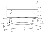
特許文献1は、このような圧電発振器の一例を示しており、その図1において、圧電発
振器1は、上蓋5と下蓋6との間に水晶振動子2が挟持され、封止されてなるパッケージ
3と、水晶振動子2を駆動するための半導体装置4とを備えてなる発振器1が記載されて
いる。上蓋5は、透光性の基材によって形成されている。また、半導体装置4はその能動
面4a側を外側にして下蓋6の外側に実装され、能動面4a側に外部接続端子11が形成
されている。
このような圧電発振器1では、外部接続端子11を利用して、基板などに容易に実装す
ることができ、小型化も容易となる。
Such a
しかしながら、特許文献1に記載したような圧電発振器1にあっては、水晶振動子2の
下蓋6と半導体装置4は、その長手方向の両端付近で電極部9などにより接合されている
。
このような構造において、圧電発振器1を基板Pにリフロー工程などにより実装すると
、加熱後に半田が硬化する過程で、図11に矢印Aで示すような力が加わる。
このため、圧電振動子2には、その両端付近に対して、矢印Bに示すような応力が作用
することになり、実装後の圧電発振器1が周波数ずれを生じる場合がある。
However, in the
In such a structure, when the
For this reason, the stress as shown by the arrow B acts on the
本発明は、以上の課題を解決するためになされたもので、実装が容易で小型化を図るこ
とができ、実装後の周波数ずれを防止できる圧電発振器を提供することを目的とする。
The present invention has been made to solve the above-described problems, and an object of the present invention is to provide a piezoelectric oscillator that can be easily mounted and can be miniaturized, and that can prevent frequency deviation after mounting.
本発明は、上述の課題の少なくとも一部を解決するためになされたものであり、以下の
形態又は適用例として実現することが可能である。
SUMMARY An advantage of some aspects of the invention is to solve at least a part of the problems described above, and the invention can be implemented as the following forms or application examples.
[適用例1]
圧電振動子と、該圧電振動子を発振させる発振回路を備える半導体装置とを接合した圧
電発振器において、前記半導体装置は、能動面に実装端子を有し、かつ前記能動面と対向
する面に接続端子を有し、前記圧電振動子は、前記接続端子と接続される電極パッドを有
し、前記接続端子が、前記能動面と対向する面の中央部に形成され、該中央部において前
記圧電振動子と接合されていることを特徴とする圧電発振器。
上記構成によれば、半導体装置に圧電振動子を重ねて接合した構成であり、全体として
コンパクトに形成することができる。
また、半導体装置の能動面を利用して、基板等へ容易に実装することができる。
さらには、前記半導体装置の前記接続端子が、前記非能動面の中央部に形成され、該中
央部において前記振動子パッケージに対して接合されている。つまり、半導体装置と振動
子パッケージは半導体装置の非能動面の中央部で接続されているので、能動面側が基板に
実装される際に、リフロー工程などにおいて応力が働くことで、半導体装置に歪みを生じ
ても、該半導体装置と振動子パッケージは互いに、中央部で接合されているので、振動子
パッケージの長さ方向の端部などに対して応力が作用することがない。このため、振動子
パッケージに収容されている圧電振動片に対して、変形応力等が作用することがなく、応
力の作用に起因する周波数ずれも生じない。
かくして、実装が容易で小型化を図ることができる圧電発振器について、実装後の周波
数ずれを防止できる圧電発振器を提供することができる。
なお、本発明で、「前記非能動面の中央部」とは、半導体装置の非能動面の正確な中心
点を指すのではなく、正確な中心点に近接した領域を指している。つまり、その部分で振
動子パッケージに接合されても、振動子パッケージが実質的に歪みを生じることのない範
囲が当該領域としての「中心部」である。
[Application Example 1]
In a piezoelectric oscillator in which a piezoelectric vibrator and a semiconductor device including an oscillation circuit that oscillates the piezoelectric vibrator are joined, the semiconductor device has a mounting terminal on an active surface and is connected to a surface facing the active surface The piezoelectric vibrator has an electrode pad connected to the connection terminal, and the connection terminal is formed at a central portion of the surface facing the active surface, and the piezoelectric vibration is formed at the central portion. A piezoelectric oscillator characterized by being joined to a child.
According to the above configuration, the piezoelectric vibrator is overlapped and joined to the semiconductor device, and can be formed compact as a whole.
Further, it can be easily mounted on a substrate or the like by using the active surface of the semiconductor device.
Furthermore, the connection terminal of the semiconductor device is formed at a central portion of the non-active surface, and is bonded to the vibrator package at the central portion. In other words, since the semiconductor device and the vibrator package are connected at the center of the non-active surface of the semiconductor device, when the active surface side is mounted on the substrate, stress is exerted in the reflow process or the like, causing distortion in the semiconductor device. Even if this occurs, since the semiconductor device and the vibrator package are bonded to each other at the center, no stress acts on the end of the vibrator package in the longitudinal direction. For this reason, deformation stress or the like does not act on the piezoelectric vibrating reed housed in the vibrator package, and no frequency shift caused by the action of stress occurs.
Thus, a piezoelectric oscillator that can be easily mounted and can be miniaturized can prevent a frequency shift after mounting.
In the present invention, the “center portion of the inactive surface” does not indicate the exact center point of the inactive surface of the semiconductor device, but indicates a region close to the accurate center point. That is, even if the portion is bonded to the vibrator package, a range in which the vibrator package does not substantially distort is the “center portion” as the region.
[適用例2]
上記構成において、前記接続端子が、前記非能動面の長手方向の中心線上であって、短
手方向の中央部に設けられていることを特徴とする。
「前記非能動面の長手方向の中心線上であって、短手方向の中央部」とは、前記した「
前記非能動面の中央部」の最も理想的な位置を意味している。このような位置に半導体装
置の前記接続端子を形成すると、その長さ方向の完全な中間位置となるので、前記した実
装時であるリフロー時などにおいて、接合相手である振動子パッケージを変形あるいは歪
がませるような応力が働くことがない。
[Application Example 2]
The said structure WHEREIN: The said connection terminal is provided on the centerline of the longitudinal direction of the said inactive surface, Comprising: It is characterized by the above-mentioned.
“On the center line in the longitudinal direction of the non-active surface and in the center in the short direction” means the above-mentioned “
It means the most ideal position of “the central part of the inactive surface”. If the connection terminal of the semiconductor device is formed at such a position, it becomes a complete intermediate position in the length direction, so that the resonator package as a bonding partner is deformed or distorted at the time of reflowing at the time of mounting. There is no stress acting on it.
[適用例3]
上記構成において、前記接続端子が、前記非能動面の短手方向に沿った仮想の中心線上
であって、長手方向の中央部に設けられていることを特徴とする。
「前記非能動面の短手方向の中心線上であって、長手方向の中央部」とは、前記した「
前記非能動面の中央部」の一例であり、比較的好ましい位置を意味している。このような
位置に半導体装置の前記接続端子を形成した場合においても、その長さ方向のほぼ中間位
置となるので、前記した実装時であるリフロー時などにおいて、接合相手である振動子パ
ッケージを変形あるいは歪がませるような応力が働くことがない。
[Application Example 3]
The said structure WHEREIN: The said connection terminal is provided on the virtual center line along the transversal direction of the said inactive surface, Comprising: It is characterized by the above-mentioned.
“On the center line in the short direction of the non-active surface and in the longitudinal center” means the above-mentioned “
It is an example of “the central portion of the non-active surface” and means a relatively preferable position. Even when the connection terminal of the semiconductor device is formed at such a position, it becomes a substantially intermediate position in the length direction, so that the vibrator package as a joining partner is deformed at the time of reflowing at the time of mounting as described above. Or there is no stress that causes distortion.
[適用例4]
上記構成において、前記接続端子が、前記非能動面の中心点から対角方向にずれて2つ
設けられていることを特徴とする。
上記構成によれば、半導体装置の前記接続端子を、非能動面の中心点から対角方向にず
れて2つ設ける場合には、振動子パッケージとの接合箇所の位置が、圧電振動片の長さ方
向に対して傾斜する方向となり、このような方向に沿った2点に、仮にリフロー時などに
応力が作用しても、該圧電振動片を歪ませるようなことがないので、周波数ずれを生じな
い。
[Application Example 4]
In the above configuration, two connection terminals are provided so as to be shifted diagonally from the center point of the inactive surface.
According to the above configuration, when two connection terminals of the semiconductor device are provided diagonally away from the center point of the non-active surface, the position of the joint portion with the vibrator package is the length of the piezoelectric vibrating piece. Even if stress is applied to two points along such a direction during reflow, the piezoelectric vibrating piece will not be distorted. Does not occur.
[適用例5]
上記構成において、半導体装置と前記圧電振動子との間に弾性率の低い樹脂を充填した
ことを特徴とする。
上記構成によれば、半導体装置側から伝えられるリフロー時など実装時の応力は、弾性
率の低い樹脂により伝えられて、その応力が緩和されることで、圧電振動片へ伝えられる
ことが防止される。
また、当該樹脂は半導体装置と圧電振動子との間に介在して、両者の接合をより強固な
ものとすることができる。
[Application Example 5]
In the above structure, a resin having a low elastic modulus is filled between the semiconductor device and the piezoelectric vibrator.
According to the above configuration, the stress at the time of mounting such as reflow transmitted from the semiconductor device side is transmitted by the resin having a low elastic modulus, and the stress is relaxed to prevent the stress from being transmitted to the piezoelectric vibrating piece. The
In addition, the resin can be interposed between the semiconductor device and the piezoelectric vibrator to further strengthen the bonding between the two.
[適用例6]
上記構成において、前記圧電振動子は、パッケージと該パッケージ内に収容された振動
片を有し、前記振動片は前記パッケージ内で、片持ち式に固定されていることを特徴とす
る。
上記構成によれば、圧電振動片が片側で支持されているから、仮に、実装時においてリ
フローの際に作用する応力が振動子パッケージに伝えられても、圧電振動片の長さ方向の
一端しか振動子パッケージに接続されておらず、該パッケージから圧電振動片に応力が作
用する事態はほとんどない。
[Application Example 6]
In the above configuration, the piezoelectric vibrator includes a package and a vibrating piece accommodated in the package, and the vibrating piece is fixed in a cantilever manner in the package.
According to the above configuration, since the piezoelectric vibrating piece is supported on one side, even if a stress acting during reflow is transmitted to the vibrator package at the time of mounting, only one end of the piezoelectric vibrating piece in the length direction is provided. There is almost no situation where stress is applied to the piezoelectric vibrating piece from the package without being connected to the vibrator package.
[適用例7]
上記構成において、前記圧電振動子は、水晶により形成した第1および第2の基板と、
振動片ならびに前記第1および前記第2の基板に挟まれて固定された枠部を一体に結合し
た基板とを有し、前記振動片は、前記枠部から片持ち式に延出することを特徴とする。
上記構成によれば、圧電振動片とこれを収容するパッケージの材料が同一であるから温
度変化による線膨張係数が同じである。したがって、実装時においてリフローの際などの
応力以外に、温度の変化による応力が作用することなども防止でき、周波数のずれを一層
確実に防止することができる。
[Application Example 7]
In the above configuration, the piezoelectric vibrator includes first and second substrates formed of quartz,
A vibration piece and a substrate integrally joined with a frame portion sandwiched and fixed between the first and second substrates, and the vibration piece extends from the frame portion in a cantilevered manner. Features.
According to the above configuration, the material of the piezoelectric vibrating piece and the package that accommodates the piezoelectric vibrating piece is the same, so the linear expansion coefficient due to temperature change is the same. Therefore, it is possible to prevent stress due to temperature change in addition to stress during reflow during mounting, and it is possible to more reliably prevent frequency shift.
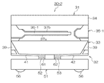
図1は、本発明の圧電発振器の第1の実施形態を示す概略断面図である。
図において、圧電発振器30は、圧電振動子31と、この圧電振動子31のパッケージ
32内に収容した圧電振動片35を発振させる発振回路を備える半導体装置51とを接合
して形成されている。
FIG. 1 is a schematic sectional view showing a first embodiment of the piezoelectric oscillator of the present invention.
In the figure, a piezoelectric oscillator 30 is formed by joining a
この実施形態において、圧電振動子31は、図1に示すように、第1および第2の基板
33,34を含む前記パッケージ32と、これら第1および第2の基板33,34に挟ま
れて固定された圧電振動片35を備えている。
第1および第2の基板33,34は、好ましくは、光を透過する平坦な板であり、ガラ
スか、より好ましくは圧電振動片35と同じ材料で形成されている。すなわち、この実施
形態では、第1および第2の基板33,34はともに水晶で形成されていると好ましい。
In this embodiment, as shown in FIG. 1, the
The first and
圧電振動片35は、圧電材料により形成されている。圧電材料として、例えば、この実
施形態では水晶が使用されており、水晶以外にもタンタル酸リチウム,ニオブ酸リチウム
等の圧電材料を利用することができる。
特に、この圧電振動片35は矩形の水晶の板の外周縁の厚みを残して、エッチングによ
り中央部の厚みを薄く加工して励振領域を形成した逆メサ型のAT振動片が使用されてい
る。圧電振動片は、このような形態以外にも、逆メサ型でない矩形(第1および第2の基
板の内側に凹状部を形成して励振を可能とした場合)や、音叉型の振動片などを用いるこ
ともできる。
The piezoelectric vibrating
In particular, the piezoelectric vibrating
第1および第2の基板33,34は、圧電振動片35を間に挟み込んで接合されている
。このような接合は種々の接合法により接合できる。例えば、これら第1および第2の基
板33,34と圧電振動片35とは、接合面にプラズマを照射することにより共有結合を
発生させる、いわゆる直接接合によって接合したり、金−スズによる合金接合することが
できる。あるいは、第1および第2の基板33,34をガラスとした場合には陽極接合に
より接合することができる。
圧電振動片35の励振領域には、その表面と裏面にそれぞれクロム−金メッキなどによ
り励振電極37a,37bが形成されている。これらの励振電極は導電パターンにより圧
電振動片35の外縁の枠部分まで延長され、下方に導かれている。
The first and
In the excitation region of the piezoelectric vibrating
図2は、第1の基板33の裏面側を示している。この第1の基板33は、その四隅の箇
所に欠落部、すなわちキャスタレーション39がドライエッチングなどにより予め形成さ
れており、励振電極37a,37bから延びる導電パターンは、図2に示されているよう
に導電パターン41a,42aにより中央部に導かれている。
すなわち、延長された導電パターン41a,42aの先端には電極端子である電極パッ
ド41,42が形成されている。これら電極パッド41,42は、第1の基板32の短手
方向の寸法を2分する仮想の中心線C1上で並列に、長手方向の寸法(図1の符合Lに相
当)を2分する仮想の中心線C2に近接して設けられている。
FIG. 2 shows the back side of the
That is,
半導体装置51は、所謂ICチップであり、圧電振動子31の発振回路と温度補償回路
とを内臓した半導体素子であり、該圧電振動子31の動作の温度補償などの機能を発揮す
るものである。
図1においては、半導体装置51の下の面が能動面58であり、上の面が能動面と対向
する非能動面57である。図4に示すように、半導体装置51の能動面58には、外部接
続端子、すなわち、実装端子56が四隅部に対応して形成されている。実装端子56は、
金属バンプ、スタッドバンプなどによっても形成できるが、この実施形態では、半田ボー
ルで形成している。
The
In FIG. 1, the lower surface of the
Although it can be formed by a metal bump, a stud bump or the like, in this embodiment, it is formed by a solder ball.
他方、半導体装置51の非能動面57には、図3に示すように能動面58と接続された
貫通電極54,55が形成されている。貫通電極は、半導体装置51を形成するシリコン
基板を貫通して表裏を電気的に接続するものである。
その形成法を簡単に説明すると、まず、上記シリコン基板の表面全体に、熱酸化等によ
って酸化シリコンからなる絶縁層を形成する。次に、この絶縁層上にレジストを塗布し、
露光・現像処理により所定形状にパターニングする。続いて、このレジストをマスクとし
て、エッチング処理によりシリコン基板に複数の平面視円形状の溝部を形成する。さらに
、この溝部の内壁面を覆う絶縁層を熱酸化法等により形成して、その後、該溝部の内部つ
まり内壁面を含むシリコン基板の能動面にスパッタ法や真空蒸着法等によって下地層を形
成する。
続いて、シリコン基板の能動面58上にメッキレジストを塗布し、該メッキレジストを
上記溝部の周辺のシリコン基板が露出した開口部を有するようにパターニングし、メッキ
レジストパターンを形成する。このメッキレジストパターンをマスクにしてCu電解メッ
キ処理し、上記開口部を含む溝部の内部に銅を析出させる。これにより、溝部の内部に銅
が充填され、溝部を含む開口部に金属端子が形成される。次いで、メッキレジストパター
ンをそのままマスクにして、金属端子上に無鉛半田等のろう材からなる接合材を形成する
。
On the other hand, through
The formation method will be briefly described. First, an insulating layer made of silicon oxide is formed on the entire surface of the silicon substrate by thermal oxidation or the like. Next, a resist is applied on this insulating layer,
Patterning into a predetermined shape by exposure and development processing. Subsequently, a plurality of circular grooves in plan view are formed in the silicon substrate by etching using the resist as a mask. Further, an insulating layer covering the inner wall surface of the groove is formed by a thermal oxidation method or the like, and then an underlying layer is formed on the active surface of the silicon substrate including the inner wall surface, that is, the inner wall surface, by sputtering or vacuum deposition. To do.
Subsequently, a plating resist is applied on the
次に、メッキレジストパターンをシリコン基板から除去し、該シリコン基板をその裏面
側からバックグラインドし、シリコン基板の裏面に金属端子を露出させる。
これにより、金属端子と接合材とからなる複数の貫通電極54,55を形成することが
できる。
これにより、半導体装置51においては、貫通電極54,55を介して圧電振動片35
の駆動を制御することができる。
なお、半導体装置51の貫通電極54,55および実装端子56を露出した個所以外は
、例えばポリイミドなどにより絶縁されている。
本実施形態では、図3に示すように、各貫通電極54,55から導電パターンを延長し
、先端に接続端子52,53を形成している。これら接続端子52,53は半導体装置5
1の短手方向の寸法を2分する仮想の中心線HC1上で並列に、長手方向の寸法を2分す
る仮想の中心線HC2に近接して設けられている。しかも、半導体装置51の上に圧電振
動子31を重ねたときに、半導体装置51の接続端子52,53は、圧電振動子31の図
2で説明した第1の基板33の電極パッド41,42と一致する位置となる。これにより
、接続端子52,53を、それぞれ電極パッド41,42に対して、半田61,62で接
合することにより、圧電発振器30を形成することができる。
Next, the plating resist pattern is removed from the silicon substrate, the silicon substrate is back-ground from the back surface side, and the metal terminals are exposed on the back surface of the silicon substrate.
As a result, a plurality of through
Thereby, in the
Can be controlled.
The portions other than the portions where the through
In the present embodiment, as shown in FIG. 3, the conductive pattern is extended from each of the through
1 is provided in parallel on a virtual center line HC1 that divides the dimension in the short direction into two, and is adjacent to a virtual center line HC2 that divides the dimension in the longitudinal direction into two. Moreover, when the
本実施形態は以上のように構成されており、図1で説明したように、半導体装置51に
圧電振動子31を重ねて接合した構成なので、全体としてコンパクトに形成することがで
きる。
そして、半導体装置51の能動面58に実装端子56を設けるだけで、図示しない実装
基板等へ容易に実装することができる。
さらには、図3で説明したように、半導体装置51の接続端子52,53が、非能動面
57の中央部に形成され、図1に示したように、該中央部においてパッケージ32に対し
て接合されている。つまり、半導体装置51とパッケージ32は半導体装置51の非能動
面57の中央部で接続されている
このため、圧電発振器30の半導体装置51の能動面58側が図示しない実装基板に実
装される際に、リフロー工程などにおいて応力が働くことで、半導体装置51に歪みを生
じても、該半導体装置51とパッケージ32は互いに、中央部で接合されているので、パ
ッケージ32の長さ方向の端部などに対して応力が作用することがない。このため、パッ
ケージ32に収容されている圧電振動片35に対して、変形応力等が作用することがなく
、応力の作用に起因する周波数ずれも生じない。
かくして、実装が容易で小型化を図ることができ、実装後の周波数ずれを防止できる圧
電発振器30を提供することができる。
The present embodiment is configured as described above. As described with reference to FIG. 1, the
Then, simply by providing the mounting
Further, as described with reference to FIG. 3, the
Thus, it is possible to provide the piezoelectric oscillator 30 that can be easily mounted and reduced in size and can prevent a frequency shift after mounting.
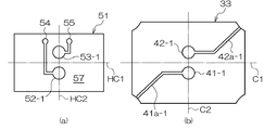
図5ないし図7は、各変形例を示している。
図5(a)において、半導体装置51の接続端子52−1,53−1は、その非能動面
57の長手方向に沿った仮想の中心線HC2上であって、短手方向の中央部に設けられて
いる。この変形例は、接続端子を設ける上では、最も理想的な位置を示している。
図5(b)に示すように、圧電振動子側である第1の基板33の電極パッド41−1,
42−1も該第1の基板33の長手方向に沿った仮想の中心線C2上であって、短手方向
の中央部に設けられている。
このような位置に半導体装置51の接続端子を形成し、第1の基板33側の電極パッド
と接合すると、それらの長さ方向の完全な中間位置となるので、図1における圧電発振器
30の実装時であるリフロー時などにおいて、接合相手であるパッケージ32を変形ある
いは歪がませるような応力が働くことがない。
5 to 7 show modifications.
In FIG. 5A, the connection terminals 52-1 and 53-1 of the
As shown in FIG. 5B, the electrode pads 41-1 of the
42-1 is also provided on the imaginary center line C2 along the longitudinal direction of the
When the connection terminal of the
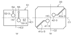
図6と図7はともに、半導体装置51の接続端子52−2,53−2(図6)、52−
3,53−3(図7)が、非能動面57の中心点HO(縦横の各寸法の中心位置)から対
角方向にずれて2つ設けられている。これに応じて、圧電振動子側である第1の基板33
の電極パッド41−2,42−2(図6)、41−3,42−3(図7)も、該第1の基
板33の中心点HO(縦横の各寸法の中心位置)から対角方向にずれて2つ設けられてい
る。
このような変形例によると、半導体装置51と図1のパッケージ32との接合箇所の位
置が、圧電振動片35の長さ方向に対して傾斜する方向となり、このような方向に沿った
2点に、仮にリフロー時などに応力が作用しても、該圧電振動片35を歪ませるようなこ
とがないので、周波数ずれを生じない。
6 and 7 are both connection terminals 52-2, 53-2 (FIG. 6), 52- of the
3, 33-3 (FIG. 7) are provided in a diagonal direction from the center point HO (center position of each dimension in the vertical and horizontal directions) of the
The electrode pads 41-2, 42-2 (FIG. 6), 41-3, 42-3 (FIG. 7) are also diagonal from the center point HO (center position of each dimension in the vertical and horizontal directions) of the
According to such a modification, the position of the joining portion between the
図8は、第2の実施形態を示している。
図8の圧電発振器30−1において、第1の実施形態に関する図1の符合と同一の符合
を付した個所は共通する構成であるから、重複する説明を省略し、以下、相違点を中心に
説明する。
FIG. 8 shows a second embodiment.
In the piezoelectric oscillator 30-1 in FIG. 8, the same reference numerals as those in FIG. 1 relating to the first embodiment are the same in configuration, and thus redundant description will be omitted. explain.
この実施形態では、半導体装置51の接続端子52,53が、非能動面57の中央部に
形成され、この中央部においてパッケージ32に対して接合されているだけでなく、半導
体装置51とパッケージ32との間に弾性率の低い樹脂65を充填したものである。
ここで、樹脂65は、例えば、シリコーン(シリカケトン)樹脂を用いることができる
。
これにより、半導体装置側51から伝えられるリフロー時など実装時の応力は、弾性率
の低い樹脂65により伝えられて、その応力が緩和されることで、圧電振動片35へ伝え
られることが防止される。
また、樹脂65は半導体装置51とパッケージ32との間に介在して、両者の接合をよ
り強固なものとすることができる。
In this embodiment, the
Here, as the resin 65, for example, a silicone (silica ketone) resin can be used.
Thereby, the stress at the time of mounting such as reflow transmitted from the
In addition, the resin 65 is interposed between the
図9は、第3の実施形態を示している。
図9の圧電発振器30−2おいて、第1の実施形態に関する図1の符合と同一の符合を
付した個所は共通する構成であるから、重複する説明を省略し、以下、相違点を中心に説
明する。
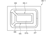
図9の圧電発振器30−2において、その圧電振動子31のパッケージ32に収容され
る圧電振動片35−1は、図10に示すように構成されている。
FIG. 9 shows a third embodiment.
In the piezoelectric oscillator 30-2 in FIG. 9, the same reference numerals as those in FIG. 1 relating to the first embodiment are the same in configuration, and thus redundant description will be omitted. Explained.
In the piezoelectric oscillator 30-2 of FIG. 9, the piezoelectric vibrating piece 35-1 accommodated in the
図10は圧電振動片35−1の概略平面図である。
図において、圧電振動片35−1は枠付き振動片であり、その枠部67の一端から振動
片が片持ち式に延出して形成されている。
すなわち、枠部67の左端部から一対の支持部68,68を介して、短冊状ないし矩形
のAT振動片本体66が延びており、先端側は固定されない自由端となっている。この振
動片本体66の表裏には励振電極37a,37bが形成されている(図9、図10)。
FIG. 10 is a schematic plan view of the piezoelectric vibrating piece 35-1.
In the figure, the piezoelectric vibrating piece 35-1 is a vibrating piece with a frame, and the vibrating piece extends from one end of the
That is, a strip-shaped or rectangular AT vibration piece
本実施形態は以上のように形成されており、圧電振動片35−1の振動片本体66が片
側で支持されているから、仮に、実装時においてリフローの際に作用する応力がパッケー
ジ32に伝えられても、圧電振動片35−1の長さ方向の一端しかパッケージ32に接続
されていないことにより、パッケージ32から圧電振動片35−1に応力が作用する事態
はほとんどない。
The present embodiment is formed as described above, and since the vibration piece
本発明は上述の実施形態に限定されない。各実施形態の各構成はこれらを適宜組み合わ
せたり、省略し、図示しない他の構成と組み合わせることができる。
圧電振動片は、図示した形状に限らず、各種の異なる形態とすることもできる。
The present invention is not limited to the above-described embodiment. Each configuration of each embodiment can be appropriately combined or omitted, and can be combined with other configurations not shown.
The piezoelectric vibrating piece is not limited to the illustrated shape, and may be various types.
30・・・圧電発振器、31・・・圧電振動子、32・・・パッケージ、33・・・第
1の基板、34・・・第2の基板、35・・・圧電振動片、51・・・半導体装置
30 ... piezoelectric oscillator, 31 ... piezoelectric vibrator, 32 ... package, 33 ... first substrate, 34 ... second substrate, 35 ... piezoelectric vibrating piece, 51 ...・ Semiconductor equipment
Claims (7)
電発振器において、
前記半導体装置は、能動面に実装端子を有し、かつ前記能動面と対向する面に接続端子
を有し、
前記圧電振動子は、前記接続端子と接続される電極パッドを有し、
前記接続端子が、前記能動面と対向する面の中央部に形成され、該中央部において前記
圧電振動子と接合されていること
を特徴とする圧電発振器。 In a piezoelectric oscillator in which a piezoelectric vibrator and a semiconductor device including an oscillation circuit that oscillates the piezoelectric vibrator are joined,
The semiconductor device has a mounting terminal on an active surface and a connection terminal on a surface facing the active surface,
The piezoelectric vibrator has an electrode pad connected to the connection terminal,
The piezoelectric oscillator, wherein the connection terminal is formed at a central portion of a surface facing the active surface, and is joined to the piezoelectric vibrator at the central portion.
けられていることを特徴とする請求項1に記載の圧電発振器。 2. The piezoelectric oscillator according to claim 1, wherein the connection terminal is provided on a center line in a longitudinal direction of the inactive surface and in a center portion in a lateral direction.
けられていることを特徴とする請求項1に記載の圧電発振器。 2. The piezoelectric oscillator according to claim 1, wherein the connection terminal is provided on a center line in a short direction of the inactive surface and in a center portion in a longitudinal direction.
を特徴とする請求項1に記載の圧電発振器。 2. The piezoelectric oscillator according to claim 1, wherein two connection terminals are provided in a diagonal direction from a center point of the inactive surface.
求項1ないし4のいずれかに記載の圧電発振器。 5. The piezoelectric oscillator according to claim 1, wherein a resin having a low elastic modulus is filled between a semiconductor device and the piezoelectric vibrator.
前記振動片は前記パッケージ内で、片持ち式に固定されていることを特徴とする請求項
1ないし5のいずれかに記載の圧電発振器。 The piezoelectric vibrator has a package and a vibrating piece accommodated in the package,
The piezoelectric oscillator according to claim 1, wherein the vibrating piece is fixed in a cantilever manner in the package.
第1および前記第2の基板に挟まれて固定された枠部を一体に結合した基板とを有し、
前記振動片は、前記枠部から片持ち式に延出することを特徴とする請求項1乃至請求項
5に記載の圧電発振器。 The piezoelectric vibrator includes first and second substrates made of quartz, and a substrate integrally connecting a vibrating piece and a frame portion sandwiched and fixed between the first and second substrates. ,
6. The piezoelectric oscillator according to claim 1, wherein the vibrating piece extends in a cantilever manner from the frame portion.
Priority Applications (1)
| Application Number | Priority Date | Filing Date | Title |
|---|---|---|---|
| JP2007304037A JP2009130665A (en) | 2007-11-26 | 2007-11-26 | Piezoelectric oscillator |
Applications Claiming Priority (1)
| Application Number | Priority Date | Filing Date | Title |
|---|---|---|---|
| JP2007304037A JP2009130665A (en) | 2007-11-26 | 2007-11-26 | Piezoelectric oscillator |
Publications (2)
| Publication Number | Publication Date |
|---|---|
| JP2009130665A true JP2009130665A (en) | 2009-06-11 |
| JP2009130665A5 JP2009130665A5 (en) | 2010-12-09 |
Family
ID=40821141
Family Applications (1)
| Application Number | Title | Priority Date | Filing Date |
|---|---|---|---|
| JP2007304037A Withdrawn JP2009130665A (en) | 2007-11-26 | 2007-11-26 | Piezoelectric oscillator |
Country Status (1)
| Country | Link |
|---|---|
| JP (1) | JP2009130665A (en) |
Cited By (5)
| Publication number | Priority date | Publication date | Assignee | Title |
|---|---|---|---|---|
| JP2011049992A (en) * | 2009-08-28 | 2011-03-10 | Seiko Instruments Inc | Piezoelectric device and method of manufacturing the piezoelectric device |
| JP2011107055A (en) * | 2009-11-20 | 2011-06-02 | Seiko Epson Corp | Pressure sensor and temperature-compensated pressure sensor |
| JP2015156597A (en) * | 2014-02-21 | 2015-08-27 | 京セラクリスタルデバイス株式会社 | Piezoelectric device and mounting structure thereof |
| JP2019068462A (en) * | 2015-03-27 | 2019-04-25 | 株式会社大真空 | Piezoelectric vibration device |
| WO2023074615A1 (en) * | 2021-10-26 | 2023-05-04 | 株式会社大真空 | Temperature sensor-equipped crystal oscillator device |
Citations (16)
| Publication number | Priority date | Publication date | Assignee | Title |
|---|---|---|---|---|
| JP2003046216A (en) * | 2001-07-30 | 2003-02-14 | Kyocera Corp | Surface-mounted electronic component, circuit board, and surface-mounted electronic component mounting structure |
| JP2003133857A (en) * | 2001-10-22 | 2003-05-09 | Citizen Watch Co Ltd | Oscillator |
| JP2004260598A (en) * | 2003-02-26 | 2004-09-16 | Kyocera Corp | Surface mount temperature compensation crystal oscillator |
| JP2004297620A (en) * | 2003-03-27 | 2004-10-21 | Kyocera Corp | Surface mount temperature compensation crystal oscillator |
| JP2005020546A (en) * | 2003-06-27 | 2005-01-20 | Kyocera Corp | Surface mount crystal oscillator |
| JP2005039791A (en) * | 2003-05-29 | 2005-02-10 | Kyocera Corp | Temperature compensated crystal oscillator |
| JP2005117188A (en) * | 2003-10-03 | 2005-04-28 | Toyo Commun Equip Co Ltd | Surface mount piezoelectric oscillator and manufacturing method thereof |
| JP2005151537A (en) * | 2003-10-24 | 2005-06-09 | Seiko Epson Corp | Piezoelectric oscillator, electronic equipment, and method of manufacturing piezoelectric oscillator |
| JP2007019310A (en) * | 2005-07-08 | 2007-01-25 | Seiko Epson Corp | Piezoelectric device, method for manufacturing the same, and electronic device |
| JP2007067173A (en) * | 2005-08-31 | 2007-03-15 | Kyocera Kinseki Corp | Electronic component |
| JP2007124590A (en) * | 2005-10-31 | 2007-05-17 | Kyocera Kinseki Corp | Piezoelectric oscillator container |
| JP2007180900A (en) * | 2005-12-28 | 2007-07-12 | Seiko Epson Corp | Crystal oscillator and manufacturing method thereof |
| JP2007228009A (en) * | 2006-02-21 | 2007-09-06 | Epson Toyocom Corp | Package and piezoelectric oscillator |
| JP2007243681A (en) * | 2006-03-09 | 2007-09-20 | Daishinku Corp | Surface-mounting type piezoelectric vibration device |
| JP2007288644A (en) * | 2006-04-19 | 2007-11-01 | Epson Toyocom Corp | Piezoelectric substrate, piezoelectric vibration element, surface mounted piezoelectric vibration element, method for manufacturing piezoelectric substrate, and surface mounted piezoelectric oscillator |
| JP2007306434A (en) * | 2006-05-12 | 2007-11-22 | Epson Toyocom Corp | Piezoelectric vibrator, and manufacturing method therefor |
-
2007
- 2007-11-26 JP JP2007304037A patent/JP2009130665A/en not_active Withdrawn
Patent Citations (16)
| Publication number | Priority date | Publication date | Assignee | Title |
|---|---|---|---|---|
| JP2003046216A (en) * | 2001-07-30 | 2003-02-14 | Kyocera Corp | Surface-mounted electronic component, circuit board, and surface-mounted electronic component mounting structure |
| JP2003133857A (en) * | 2001-10-22 | 2003-05-09 | Citizen Watch Co Ltd | Oscillator |
| JP2004260598A (en) * | 2003-02-26 | 2004-09-16 | Kyocera Corp | Surface mount temperature compensation crystal oscillator |
| JP2004297620A (en) * | 2003-03-27 | 2004-10-21 | Kyocera Corp | Surface mount temperature compensation crystal oscillator |
| JP2005039791A (en) * | 2003-05-29 | 2005-02-10 | Kyocera Corp | Temperature compensated crystal oscillator |
| JP2005020546A (en) * | 2003-06-27 | 2005-01-20 | Kyocera Corp | Surface mount crystal oscillator |
| JP2005117188A (en) * | 2003-10-03 | 2005-04-28 | Toyo Commun Equip Co Ltd | Surface mount piezoelectric oscillator and manufacturing method thereof |
| JP2005151537A (en) * | 2003-10-24 | 2005-06-09 | Seiko Epson Corp | Piezoelectric oscillator, electronic equipment, and method of manufacturing piezoelectric oscillator |
| JP2007019310A (en) * | 2005-07-08 | 2007-01-25 | Seiko Epson Corp | Piezoelectric device, method for manufacturing the same, and electronic device |
| JP2007067173A (en) * | 2005-08-31 | 2007-03-15 | Kyocera Kinseki Corp | Electronic component |
| JP2007124590A (en) * | 2005-10-31 | 2007-05-17 | Kyocera Kinseki Corp | Piezoelectric oscillator container |
| JP2007180900A (en) * | 2005-12-28 | 2007-07-12 | Seiko Epson Corp | Crystal oscillator and manufacturing method thereof |
| JP2007228009A (en) * | 2006-02-21 | 2007-09-06 | Epson Toyocom Corp | Package and piezoelectric oscillator |
| JP2007243681A (en) * | 2006-03-09 | 2007-09-20 | Daishinku Corp | Surface-mounting type piezoelectric vibration device |
| JP2007288644A (en) * | 2006-04-19 | 2007-11-01 | Epson Toyocom Corp | Piezoelectric substrate, piezoelectric vibration element, surface mounted piezoelectric vibration element, method for manufacturing piezoelectric substrate, and surface mounted piezoelectric oscillator |
| JP2007306434A (en) * | 2006-05-12 | 2007-11-22 | Epson Toyocom Corp | Piezoelectric vibrator, and manufacturing method therefor |
Cited By (6)
| Publication number | Priority date | Publication date | Assignee | Title |
|---|---|---|---|---|
| JP2011049992A (en) * | 2009-08-28 | 2011-03-10 | Seiko Instruments Inc | Piezoelectric device and method of manufacturing the piezoelectric device |
| JP2011107055A (en) * | 2009-11-20 | 2011-06-02 | Seiko Epson Corp | Pressure sensor and temperature-compensated pressure sensor |
| JP2015156597A (en) * | 2014-02-21 | 2015-08-27 | 京セラクリスタルデバイス株式会社 | Piezoelectric device and mounting structure thereof |
| JP2019068462A (en) * | 2015-03-27 | 2019-04-25 | 株式会社大真空 | Piezoelectric vibration device |
| US10771037B2 (en) | 2015-03-27 | 2020-09-08 | Daishinku Corporation | Piezoelectric resonator device |
| WO2023074615A1 (en) * | 2021-10-26 | 2023-05-04 | 株式会社大真空 | Temperature sensor-equipped crystal oscillator device |
Similar Documents
| Publication | Publication Date | Title |
|---|---|---|
| JP4600663B2 (en) | Temperature compensated piezoelectric oscillator | |
| JP2010193133A (en) | Bending vibrator piece and bending vibrator | |
| JP2006246112A (en) | Surface acoustic wave device and its manufacturing method | |
| JP2006339943A (en) | Piezoelectric device | |
| JP2013165404A (en) | Vibration device and oscillator | |
| JP6547825B2 (en) | Piezoelectric vibration device | |
| JP2007295235A (en) | Piezoelectric device | |
| JP2011166309A (en) | Piezoelectric vibrator and oscillator using the same | |
| JP2009130665A (en) | Piezoelectric oscillator | |
| JP2008099144A (en) | Piezoelectric oscillating piece and piezoelectric device | |
| JP5082968B2 (en) | Piezoelectric oscillator | |
| JP2011166308A (en) | Piezoelectric vibrator and oscillator using the same | |
| JP2009165102A (en) | Piezoelectric oscillator, and method for manufacturing piezoelectric oscillator | |
| JP5428735B2 (en) | Piezoelectric device | |
| JP5643040B2 (en) | Piezoelectric oscillator | |
| JP5341685B2 (en) | Piezoelectric device | |
| JP2009055354A (en) | Package for piezoelectric vibration device and piezoelectric vibration device | |
| JP2012029024A (en) | Bending vibration piece, vibrator, oscillator, and electronic apparatus | |
| JP5299645B2 (en) | Bending vibrator element and method for manufacturing bending vibrator | |
| JP2010093859A (en) | Tuning fork piezoelectric vibrator | |
| CN114208027A (en) | Piezoelectric vibrating plate, piezoelectric vibrating device, and method for manufacturing piezoelectric vibrating device | |
| JP2009239475A (en) | Surface mounting piezoelectric oscillator | |
| JP2009124587A (en) | Piezoelectric vibrating chip, piezoelectric vibration device, and method of manufacturing piezoelectric vibrating chip | |
| JP2008141413A (en) | Piezoelectric oscillator, and manufacturing method thereof | |
| JP2018142888A (en) | Piezoelectric oscillator |
Legal Events
| Date | Code | Title | Description |
|---|---|---|---|
| A521 | Written amendment |
Free format text: JAPANESE INTERMEDIATE CODE: A523 Effective date: 20101025 |
|
| A621 | Written request for application examination |
Effective date: 20101025 Free format text: JAPANESE INTERMEDIATE CODE: A621 |
|
| A711 | Notification of change in applicant |
Effective date: 20110729 Free format text: JAPANESE INTERMEDIATE CODE: A712 |
|
| RD03 | Notification of appointment of power of attorney |
Free format text: JAPANESE INTERMEDIATE CODE: A7423 Effective date: 20110729 |
|
| A521 | Written amendment |
Effective date: 20110819 Free format text: JAPANESE INTERMEDIATE CODE: A523 |
|
| A131 | Notification of reasons for refusal |
Free format text: JAPANESE INTERMEDIATE CODE: A131 Effective date: 20120605 |
|
| A761 | Written withdrawal of application |
Free format text: JAPANESE INTERMEDIATE CODE: A761 Effective date: 20120702 |