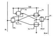
JP2009004074A - 4つのダブル・ゲートのトランジスタを備える非対称sramセル - Google Patents
4つのダブル・ゲートのトランジスタを備える非対称sramセル Download PDFInfo
- Publication number
- JP2009004074A JP2009004074A JP2008147062A JP2008147062A JP2009004074A JP 2009004074 A JP2009004074 A JP 2009004074A JP 2008147062 A JP2008147062 A JP 2008147062A JP 2008147062 A JP2008147062 A JP 2008147062A JP 2009004074 A JP2009004074 A JP 2009004074A
- Authority
- JP
- Japan
- Prior art keywords
- transistor
- gate electrode
- memory cell
- transistors
- gate
- Prior art date
- Legal status (The legal status is an assumption and is not a legal conclusion. Google has not performed a legal analysis and makes no representation as to the accuracy of the status listed.)
- Withdrawn
Links
Images

Classifications
-
- G—PHYSICS
- G11—INFORMATION STORAGE
- G11C—STATIC STORES
- G11C11/00—Digital stores characterised by the use of particular electric or magnetic storage elements; Storage elements therefor
- G11C11/21—Digital stores characterised by the use of particular electric or magnetic storage elements; Storage elements therefor using electric elements
- G11C11/34—Digital stores characterised by the use of particular electric or magnetic storage elements; Storage elements therefor using electric elements using semiconductor devices
- G11C11/40—Digital stores characterised by the use of particular electric or magnetic storage elements; Storage elements therefor using electric elements using semiconductor devices using transistors
- G11C11/41—Digital stores characterised by the use of particular electric or magnetic storage elements; Storage elements therefor using electric elements using semiconductor devices using transistors forming static cells with positive feedback, i.e. cells not needing refreshing or charge regeneration, e.g. bistable multivibrator or Schmitt trigger
- G11C11/412—Digital stores characterised by the use of particular electric or magnetic storage elements; Storage elements therefor using electric elements using semiconductor devices using transistors forming static cells with positive feedback, i.e. cells not needing refreshing or charge regeneration, e.g. bistable multivibrator or Schmitt trigger using field-effect transistors only
Landscapes
- Engineering & Computer Science (AREA)
- Microelectronics & Electronic Packaging (AREA)
- Computer Hardware Design (AREA)
- Static Random-Access Memory (AREA)
- Semiconductor Memories (AREA)
Applications Claiming Priority (1)
| Application Number | Priority Date | Filing Date | Title |
|---|---|---|---|
| FR0703955A FR2916895B1 (fr) | 2007-06-04 | 2007-06-04 | Cellule memoire sram asymetrique a 4 transistors double grille |
Publications (2)
| Publication Number | Publication Date |
|---|---|
| JP2009004074A true JP2009004074A (ja) | 2009-01-08 |
| JP2009004074A5 JP2009004074A5 (enExample) | 2011-06-30 |
Family
ID=38935890
Family Applications (1)
| Application Number | Title | Priority Date | Filing Date |
|---|---|---|---|
| JP2008147062A Withdrawn JP2009004074A (ja) | 2007-06-04 | 2008-06-04 | 4つのダブル・ゲートのトランジスタを備える非対称sramセル |
Country Status (5)
| Country | Link |
|---|---|
| US (1) | US7733688B2 (enExample) |
| EP (1) | EP2003650B1 (enExample) |
| JP (1) | JP2009004074A (enExample) |
| DE (1) | DE602008000257D1 (enExample) |
| FR (1) | FR2916895B1 (enExample) |
Families Citing this family (4)
| Publication number | Priority date | Publication date | Assignee | Title |
|---|---|---|---|---|
| US8072797B2 (en) * | 2008-07-07 | 2011-12-06 | Certichip Inc. | SRAM cell without dedicated access transistors |
| US8363455B2 (en) | 2008-12-04 | 2013-01-29 | David Rennie | Eight transistor soft error robust storage cell |
| TWI470631B (zh) * | 2011-06-01 | 2015-01-21 | Univ Nat Chiao Tung | 雙埠次臨界靜態隨機存取記憶體單元 |
| CN116230053B (zh) * | 2023-03-01 | 2023-12-22 | 芯立嘉集成电路(杭州)有限公司 | 一种四晶体管静态随机存取存储器和存取方法 |
Family Cites Families (8)
| Publication number | Priority date | Publication date | Assignee | Title |
|---|---|---|---|---|
| US6442060B1 (en) | 2000-05-09 | 2002-08-27 | Monolithic System Technology, Inc. | High-density ratio-independent four-transistor RAM cell fabricated with a conventional logic process |
| KR100560948B1 (ko) | 2004-03-31 | 2006-03-14 | 매그나칩 반도체 유한회사 | 6 트랜지스터 듀얼 포트 에스램 셀 |
| JP4795653B2 (ja) * | 2004-06-15 | 2011-10-19 | ルネサスエレクトロニクス株式会社 | 半導体記憶装置 |
| US7532501B2 (en) * | 2005-06-02 | 2009-05-12 | International Business Machines Corporation | Semiconductor device including back-gated transistors and method of fabricating the device |
| US7313012B2 (en) * | 2006-02-27 | 2007-12-25 | International Business Machines Corporation | Back-gate controlled asymmetrical memory cell and memory using the cell |
| FR2898432B1 (fr) | 2006-03-10 | 2008-04-11 | Commissariat Energie Atomique | Cellules memoire en technologie cmos double-grille dotee de transistors a deux grilles independantes |
| FR2910999B1 (fr) * | 2006-12-28 | 2009-04-03 | Commissariat Energie Atomique | Cellule memoire dotee de transistors double-grille, a grilles independantes et asymetriques |
| US7710765B2 (en) * | 2007-09-27 | 2010-05-04 | Micron Technology, Inc. | Back gated SRAM cell |
-
2007
- 2007-06-04 FR FR0703955A patent/FR2916895B1/fr not_active Expired - Fee Related
-
2008
- 2008-05-26 EP EP08354031A patent/EP2003650B1/fr not_active Ceased
- 2008-05-26 DE DE602008000257T patent/DE602008000257D1/de active Active
- 2008-05-29 US US12/155,074 patent/US7733688B2/en not_active Expired - Fee Related
- 2008-06-04 JP JP2008147062A patent/JP2009004074A/ja not_active Withdrawn
Also Published As
| Publication number | Publication date |
|---|---|
| FR2916895A1 (fr) | 2008-12-05 |
| DE602008000257D1 (de) | 2009-12-17 |
| US20080298118A1 (en) | 2008-12-04 |
| FR2916895B1 (fr) | 2009-08-28 |
| EP2003650B1 (fr) | 2009-11-04 |
| EP2003650A1 (fr) | 2008-12-17 |
| US7733688B2 (en) | 2010-06-08 |
Similar Documents
| Publication | Publication Date | Title |
|---|---|---|
| JP4822791B2 (ja) | 半導体記憶装置 | |
| JP3906166B2 (ja) | 半導体記憶装置 | |
| US7511989B2 (en) | Memory cells in double-gate CMOS technology provided with transistors with two independent gates | |
| US8654569B2 (en) | 10T SRAM cell with near dual port functionality | |
| US8159863B2 (en) | 6T SRAM cell with single sided write | |
| US20110103137A1 (en) | Source controlled sram | |
| US8164945B2 (en) | 8T SRAM cell with two single sided ports | |
| JP2002368135A (ja) | 半導体記憶装置 | |
| US7474583B2 (en) | Semiconductor memory device | |
| JP2010140534A (ja) | 半導体記憶装置 | |
| US10062419B2 (en) | Digtial circuit structures | |
| JP5057757B2 (ja) | 半導体集積回路 | |
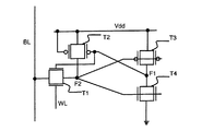
| JP2009004074A (ja) | 4つのダブル・ゲートのトランジスタを備える非対称sramセル | |
| US8179715B2 (en) | 8T SRAM cell with four load transistors | |
| KR101705172B1 (ko) | 반도체 메모리 장치 | |
| JP2008047190A (ja) | 半導体装置 | |
| US8339839B2 (en) | SRAM cell for single sided write | |
| JP2007323770A (ja) | Sram | |
| JP2008135169A (ja) | 半導体記憶装置 | |
| JP4127523B2 (ja) | 半導体集積回路およびその駆動方法 | |
| JP2011090782A (ja) | 半導体記憶装置 | |
| CN119724290A (zh) | 存储器器件、写入辅助电路和方法 | |
| JP2013054793A (ja) | Sramおよびその制御方法 | |
| JP2011071530A (ja) | 半導体記憶装置 | |
| JP2011076673A (ja) | 半導体記憶装置 |
Legal Events
| Date | Code | Title | Description |
|---|---|---|---|
| A521 | Written amendment |
Free format text: JAPANESE INTERMEDIATE CODE: A523 Effective date: 20110517 |
|
| A621 | Written request for application examination |
Free format text: JAPANESE INTERMEDIATE CODE: A621 Effective date: 20110517 |
|
| A761 | Written withdrawal of application |
Free format text: JAPANESE INTERMEDIATE CODE: A761 Effective date: 20120919 |
|
| A521 | Written amendment |
Free format text: JAPANESE INTERMEDIATE CODE: A821 Effective date: 20120919 |