JP2008529290A - 照射システム、具体的には、半導体リソグラフにおける投影露光装置のための照射システム - Google Patents
照射システム、具体的には、半導体リソグラフにおける投影露光装置のための照射システム Download PDFInfo
- Publication number
- JP2008529290A JP2008529290A JP2007552559A JP2007552559A JP2008529290A JP 2008529290 A JP2008529290 A JP 2008529290A JP 2007552559 A JP2007552559 A JP 2007552559A JP 2007552559 A JP2007552559 A JP 2007552559A JP 2008529290 A JP2008529290 A JP 2008529290A
- Authority
- JP
- Japan
- Prior art keywords
- irradiation system
- rod integrator
- axis
- rotation angle
- homogenizing
- Prior art date
- Legal status (The legal status is an assumption and is not a legal conclusion. Google has not performed a legal analysis and makes no representation as to the accuracy of the status listed.)
- Pending
Links
Images


Classifications
-
- G—PHYSICS
- G03—PHOTOGRAPHY; CINEMATOGRAPHY; ANALOGOUS TECHNIQUES USING WAVES OTHER THAN OPTICAL WAVES; ELECTROGRAPHY; HOLOGRAPHY
- G03F—PHOTOMECHANICAL PRODUCTION OF TEXTURED OR PATTERNED SURFACES, e.g. FOR PRINTING, FOR PROCESSING OF SEMICONDUCTOR DEVICES; MATERIALS THEREFOR; ORIGINALS THEREFOR; APPARATUS SPECIALLY ADAPTED THEREFOR
- G03F7/00—Photomechanical, e.g. photolithographic, production of textured or patterned surfaces, e.g. printing surfaces; Materials therefor, e.g. comprising photoresists; Apparatus specially adapted therefor
- G03F7/70—Microphotolithographic exposure; Apparatus therefor
- G03F7/70058—Mask illumination systems
- G03F7/70075—Homogenization of illumination intensity in the mask plane by using an integrator, e.g. fly's eye lens, facet mirror or glass rod, by using a diffusing optical element or by beam deflection
-
- G—PHYSICS
- G03—PHOTOGRAPHY; CINEMATOGRAPHY; ANALOGOUS TECHNIQUES USING WAVES OTHER THAN OPTICAL WAVES; ELECTROGRAPHY; HOLOGRAPHY
- G03F—PHOTOMECHANICAL PRODUCTION OF TEXTURED OR PATTERNED SURFACES, e.g. FOR PRINTING, FOR PROCESSING OF SEMICONDUCTOR DEVICES; MATERIALS THEREFOR; ORIGINALS THEREFOR; APPARATUS SPECIALLY ADAPTED THEREFOR
- G03F7/00—Photomechanical, e.g. photolithographic, production of textured or patterned surfaces, e.g. printing surfaces; Materials therefor, e.g. comprising photoresists; Apparatus specially adapted therefor
- G03F7/70—Microphotolithographic exposure; Apparatus therefor
- G03F7/70058—Mask illumination systems
- G03F7/70091—Illumination settings, i.e. intensity distribution in the pupil plane or angular distribution in the field plane; On-axis or off-axis settings, e.g. annular, dipole or quadrupole settings; Partial coherence control, i.e. sigma or numerical aperture [NA]
- G03F7/70108—Off-axis setting using a light-guiding element, e.g. diffractive optical elements [DOEs] or light guides
-
- G—PHYSICS
- G03—PHOTOGRAPHY; CINEMATOGRAPHY; ANALOGOUS TECHNIQUES USING WAVES OTHER THAN OPTICAL WAVES; ELECTROGRAPHY; HOLOGRAPHY
- G03F—PHOTOMECHANICAL PRODUCTION OF TEXTURED OR PATTERNED SURFACES, e.g. FOR PRINTING, FOR PROCESSING OF SEMICONDUCTOR DEVICES; MATERIALS THEREFOR; ORIGINALS THEREFOR; APPARATUS SPECIALLY ADAPTED THEREFOR
- G03F7/00—Photomechanical, e.g. photolithographic, production of textured or patterned surfaces, e.g. printing surfaces; Materials therefor, e.g. comprising photoresists; Apparatus specially adapted therefor
- G03F7/70—Microphotolithographic exposure; Apparatus therefor
- G03F7/70058—Mask illumination systems
- G03F7/70141—Illumination system adjustment, e.g. adjustments during exposure or alignment during assembly of illumination system
-
- G—PHYSICS
- G03—PHOTOGRAPHY; CINEMATOGRAPHY; ANALOGOUS TECHNIQUES USING WAVES OTHER THAN OPTICAL WAVES; ELECTROGRAPHY; HOLOGRAPHY
- G03F—PHOTOMECHANICAL PRODUCTION OF TEXTURED OR PATTERNED SURFACES, e.g. FOR PRINTING, FOR PROCESSING OF SEMICONDUCTOR DEVICES; MATERIALS THEREFOR; ORIGINALS THEREFOR; APPARATUS SPECIALLY ADAPTED THEREFOR
- G03F7/00—Photomechanical, e.g. photolithographic, production of textured or patterned surfaces, e.g. printing surfaces; Materials therefor, e.g. comprising photoresists; Apparatus specially adapted therefor
- G03F7/70—Microphotolithographic exposure; Apparatus therefor
- G03F7/70058—Mask illumination systems
- G03F7/7015—Details of optical elements
- G03F7/70158—Diffractive optical elements
Landscapes
- Physics & Mathematics (AREA)
- General Physics & Mathematics (AREA)
- Exposure And Positioning Against Photoresist Photosensitive Materials (AREA)
- Exposure Of Semiconductors, Excluding Electron Or Ion Beam Exposure (AREA)
- Optical Elements Other Than Lenses (AREA)
- Lenses (AREA)
Abstract
Description
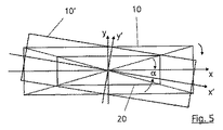
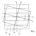
この目的は、非対称的な瞳孔分布のために、少なくとも、非回転対称の光分布をもたらす光学素子、及び/もしくは、均一化素子が、x−y座標系のz軸を形成する光軸を回転軸にして回転可能に支持され、瞳孔分布が、1つの軸上、もしくはx−y座標系を回転角度a分回転させて回転角度aによって新たに形成されたx’−y’座標系の1つの軸を基準にして対称的に位置するように、少なくとも1つの回転角度aを設定することが可能であるという事実に基づいて、本発明によって達成される。
本発明のさらなる実質的な効果は、独創的に回転可能なセッティングと、光学素子及び均一化素子を共に搭載したこととによって、同一の照射システムが、垂直パターンもしくは水平パターンと、傾斜パターンとの双方を撮像するのに適しているということである。全ての素子は、“通常動作”のx−y座標系では“通常位置”にある。ウエハー上に傾斜パターンを生成することが望まれているときには、単に、適切な回転角度を設定する必要があるだけである。適切な回転角度のセッティングを大きな経費を要することなく実行できるため、顧客の要求に従う非常に汎用的に使用可能な照射システムがもたらされる。
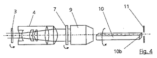
本発明に基づく解決策は、明確に、長方形の断面を有するロッドではなく、少なくとも略正方形の側面を有するロッドを使用するときにいつでも、特別な効果を伴って使用され得る。この場合、光損失、及び領域の減小は、結局、明確に長方形のロッドの場合よりも実質的に小さくなる。
均一化素子として例えばロッドインテグレータもしくはハニカム集光器を有する照射システムを備える投影露光装置の構造及び作動形態は、原理上周知であるため、その構造及び作動形態については、以下にごく簡単に説明する。一例として、さらなる詳細については、ドイツ特許公報DE 101 32 988 A1(米国特許公報US 6,707,537 B2)が参照される。そして、ドイツ特許公報DE 101 32 988 A1(米国特許公報US 6,707,537 B2)は、参照されることにより、本願における主題の開示の一部をなす。
Claims (12)
- 照射システムであり、光源が発する光を有し、光軸と光学素子とを有し、具体的には、半導体リソグラフにおける投影露光装置のための照射システムであり、光線の瞳孔分布を生成するための少なくとも1つの光学素子を有し、前記光の強度を均一化するための均一化素子を有する照射システムであって、
非対称的な瞳孔分布のために、非回転対称の光分布をもたらす少なくとも1つの前記光学素子(3,7)、及び/もしくは前記均一化素子が、x−y座標系のz軸を形成する前記光軸を回転軸として回転可能に支持され、
前記瞳孔分布が、1つの軸上に位置、もしくは、前記x−y座標系を回転角度a分回転させて、該回転角度aによって新たに形成されるx’−y’座標系の1つの軸を基準にして対称的に位置するように、少なくとも1つの前記回転角度aを設定することが可能である
ことを特徴とする照射システム。 - 請求項1に記載の照射システムであって、
少なくとも1つの回転可能な光学素子(3,7)、及び前記均一化素子(10)は、同一の回転角度分回転される
ことを特徴とする照射システム。 - 請求項1に記載の照射システムであって、
少なくとも1つの回転可能な光学素子(3,7)、及び前記均一化素子(10)は、異なる回転角度分回転される
ことを特徴とする照射システム。 - 請求項1乃至請求項3のいずれかに記載の照射システムであって、
前記均一化素子として配設されているのは、非対称的な瞳孔分布のために回転角度a分回転可能な長方形のロッドインテグレータ(10)である
ことを特徴とする照射システム。 - 請求項4に記載の照射システムであって、
前記ロッドインテグレータ(10)の断面は、少なくとも略正方形である
ことを特徴とする照射システム。 - 請求項4または請求項5に記載の照射システムであって、
前記ロッドインテグレータ(10)は、インカップリング・オプティクス(9)と、視野絞り(11)を有する領域面との間に配置されている
ことを特徴とする照射システム。 - 請求項1乃至請求項6のいずれかに記載の照射システムであって、
前記複数の光学素子(3,7)は、前記光線の方向における前記均一化素子(10,24)の上流に位置決めされた回折光学素子及び/もしくは屈折光学素子である
ことを特徴とする照射システム。 - 請求項4乃至請求項7のいずれかに記載の照射システムであって、
前記ロッドインテグレータ(10,10’’)は、交換可能に前記照射システムに配置され、
正方形の断面を有するロッドインテグレータ(10’’)は、回転角度の設定に関連して、長方形の断面を有するロッドインテグレータ(10)の代わりに配設される
ことを特徴とする照射システム。 - 請求項8に記載の照射システムであって、
長方形の断面(10)を有する前記ロッドインテグレータの端面における対角線の長さは、少なくとも、正方形の断面を有する前記ロッドインテグレータ(10’’)における端部の長さとほぼ一致している
ことを特徴とする照射システム。 - 請求項8または請求項9に記載の照射システムであって、
前記光線の方向における前記ロッドインテグレータ(10,10’’)の上流に配置された複数の屈折光学素子(7)は、交換可能に配置されている
ことを特徴とする照射システム。 - 請求項1に記載の照射システムであって、
均一化素子として、ハニカム集光器(24)が配設されている
ことを特徴とする照射システム。 - 請求項1乃至請求項11のいずれかに記載の照射システムを有する、半導体リソグラフにおける投影露光装置。
Applications Claiming Priority (2)
| Application Number | Priority Date | Filing Date | Title |
|---|---|---|---|
| DE102005004216A DE102005004216A1 (de) | 2005-01-29 | 2005-01-29 | Beleuchtungssystem, insbesondere für eine Projektionsbelichtungsanlage in der Halbleiterlithographie |
| PCT/EP2006/000535 WO2006079486A2 (en) | 2005-01-29 | 2006-01-21 | Illumination system, in particular for a projection exposure machine in semiconductor lithography |
Publications (2)
| Publication Number | Publication Date |
|---|---|
| JP2008529290A true JP2008529290A (ja) | 2008-07-31 |
| JP2008529290A5 JP2008529290A5 (ja) | 2009-02-05 |
Family
ID=36084237
Family Applications (1)
| Application Number | Title | Priority Date | Filing Date |
|---|---|---|---|
| JP2007552559A Pending JP2008529290A (ja) | 2005-01-29 | 2006-01-21 | 照射システム、具体的には、半導体リソグラフにおける投影露光装置のための照射システム |
Country Status (6)
| Country | Link |
|---|---|
| US (1) | US20080273186A1 (ja) |
| EP (1) | EP1842102A2 (ja) |
| JP (1) | JP2008529290A (ja) |
| KR (1) | KR20070100905A (ja) |
| DE (1) | DE102005004216A1 (ja) |
| WO (1) | WO2006079486A2 (ja) |
Cited By (2)
| Publication number | Priority date | Publication date | Assignee | Title |
|---|---|---|---|---|
| JP2013077022A (ja) * | 2006-12-01 | 2013-04-25 | Seiko Epson Corp | 光源装置、画像表示装置、プロジェクタ、照明装置、及びモニタ装置 |
| JP2021511546A (ja) * | 2018-01-23 | 2021-05-06 | カール・ツァイス・エスエムティー・ゲーエムベーハー | 投影リソグラフィ用の照明光学デバイス |
Families Citing this family (6)
| Publication number | Priority date | Publication date | Assignee | Title |
|---|---|---|---|---|
| US8164739B2 (en) * | 2007-09-28 | 2012-04-24 | Asml Holding N.V. | Controlling fluctuations in pointing, positioning, size or divergence errors of a beam of light for optical apparatus |
| JP6494339B2 (ja) * | 2015-03-10 | 2019-04-03 | キヤノン株式会社 | 照明光学系、露光装置、及び物品の製造方法 |
| DE102018201010A1 (de) * | 2018-01-23 | 2019-07-25 | Carl Zeiss Smt Gmbh | Beleuchtungsoptik für die Projektionslithographie |
| CN112305863B (zh) * | 2019-07-25 | 2021-12-03 | 上海微电子装备(集团)股份有限公司 | 照明系统、光瞳椭圆度补偿方法及光刻机 |
| CN112445005B (zh) * | 2019-08-29 | 2023-08-11 | 深圳市中光工业技术研究院 | 激光光源及激光光源系统 |
| CN112445076B (zh) * | 2019-08-30 | 2022-04-22 | 上海微电子装备(集团)股份有限公司 | 光刻机、曝光系统及实现离轴照明的方法与离轴照明装置 |
Citations (6)
| Publication number | Priority date | Publication date | Assignee | Title |
|---|---|---|---|---|
| JPH07221007A (ja) * | 1994-01-31 | 1995-08-18 | Nec Corp | 縮小投影露光装置 |
| JPH0883743A (ja) * | 1994-09-09 | 1996-03-26 | Nikon Corp | 照明光学装置 |
| JPH11354424A (ja) * | 1998-06-04 | 1999-12-24 | Canon Inc | 照明装置及びそれを用いた投影露光装置 |
| JP2001313250A (ja) * | 2000-02-25 | 2001-11-09 | Nikon Corp | 露光装置、その調整方法、及び前記露光装置を用いるデバイス製造方法 |
| JP2002043221A (ja) * | 2000-07-05 | 2002-02-08 | Asm Lithography Bv | リソグラフィ投影装置 |
| JP2002158157A (ja) * | 2000-11-17 | 2002-05-31 | Nikon Corp | 照明光学装置および露光装置並びにマイクロデバイスの製造方法 |
Family Cites Families (10)
| Publication number | Priority date | Publication date | Assignee | Title |
|---|---|---|---|---|
| US6897942B2 (en) * | 1990-11-15 | 2005-05-24 | Nikon Corporation | Projection exposure apparatus and method |
| US6285443B1 (en) * | 1993-12-13 | 2001-09-04 | Carl-Zeiss-Stiftung | Illuminating arrangement for a projection microlithographic apparatus |
| EP0687956B2 (de) * | 1994-06-17 | 2005-11-23 | Carl Zeiss SMT AG | Beleuchtungseinrichtung |
| JPH09199390A (ja) * | 1996-01-16 | 1997-07-31 | Hitachi Ltd | パターン形成方法、投影露光装置および半導体装置の製造方法 |
| DE10132988B4 (de) * | 2001-07-06 | 2005-07-28 | Carl Zeiss Smt Ag | Projektionsbelichtungsanlage |
| DE10158921A1 (de) * | 2001-11-30 | 2003-06-26 | Zeiss Carl Smt Ag | Verfahren zum Bestimmen von mindestens einer Kenngröße, die für die Beleuchtungswinkelverteilung einer der Beleuchtung eines Gegenstandes dienenden Lichtquelle einer Projektionsbelichtungsanlage charakteristisch ist |
| JP4332331B2 (ja) * | 2002-08-05 | 2009-09-16 | キヤノン株式会社 | 露光方法 |
| EP1434092A1 (en) * | 2002-12-23 | 2004-06-30 | ASML Netherlands B.V. | Lithographic apparatus, device manufacturing method, and device manufactured thereby |
| US20040207829A1 (en) * | 2003-04-17 | 2004-10-21 | Asml Netherlands, B.V. | Illuminator controlled tone reversal printing |
| US20050134820A1 (en) * | 2003-12-22 | 2005-06-23 | Asml Netherlands B.V. | Method for exposing a substrate, patterning device, and lithographic apparatus |
-
2005
- 2005-01-29 DE DE102005004216A patent/DE102005004216A1/de not_active Withdrawn
-
2006
- 2006-01-21 WO PCT/EP2006/000535 patent/WO2006079486A2/en active Application Filing
- 2006-01-21 KR KR1020077019609A patent/KR20070100905A/ko not_active Application Discontinuation
- 2006-01-21 EP EP06722978A patent/EP1842102A2/en not_active Withdrawn
- 2006-01-21 JP JP2007552559A patent/JP2008529290A/ja active Pending
- 2006-01-21 US US11/814,685 patent/US20080273186A1/en not_active Abandoned
Patent Citations (6)
| Publication number | Priority date | Publication date | Assignee | Title |
|---|---|---|---|---|
| JPH07221007A (ja) * | 1994-01-31 | 1995-08-18 | Nec Corp | 縮小投影露光装置 |
| JPH0883743A (ja) * | 1994-09-09 | 1996-03-26 | Nikon Corp | 照明光学装置 |
| JPH11354424A (ja) * | 1998-06-04 | 1999-12-24 | Canon Inc | 照明装置及びそれを用いた投影露光装置 |
| JP2001313250A (ja) * | 2000-02-25 | 2001-11-09 | Nikon Corp | 露光装置、その調整方法、及び前記露光装置を用いるデバイス製造方法 |
| JP2002043221A (ja) * | 2000-07-05 | 2002-02-08 | Asm Lithography Bv | リソグラフィ投影装置 |
| JP2002158157A (ja) * | 2000-11-17 | 2002-05-31 | Nikon Corp | 照明光学装置および露光装置並びにマイクロデバイスの製造方法 |
Cited By (2)
| Publication number | Priority date | Publication date | Assignee | Title |
|---|---|---|---|---|
| JP2013077022A (ja) * | 2006-12-01 | 2013-04-25 | Seiko Epson Corp | 光源装置、画像表示装置、プロジェクタ、照明装置、及びモニタ装置 |
| JP2021511546A (ja) * | 2018-01-23 | 2021-05-06 | カール・ツァイス・エスエムティー・ゲーエムベーハー | 投影リソグラフィ用の照明光学デバイス |
Also Published As
| Publication number | Publication date |
|---|---|
| WO2006079486A2 (en) | 2006-08-03 |
| EP1842102A2 (en) | 2007-10-10 |
| US20080273186A1 (en) | 2008-11-06 |
| DE102005004216A1 (de) | 2006-08-03 |
| WO2006079486A3 (en) | 2006-10-05 |
| KR20070100905A (ko) | 2007-10-12 |
Similar Documents
| Publication | Publication Date | Title |
|---|---|---|
| JP3993335B2 (ja) | リソグラフィ装置と方法 | |
| JP2008544531A (ja) | 瞳ファセットミラー上に減衰素子を備えた二重ファセット照明光学系 | |
| JP5026788B2 (ja) | マイクロリソグラフィの照明システム | |
| US8025427B2 (en) | Filter device for the compensation of an asymmetric pupil illumination | |
| JP2008529290A (ja) | 照射システム、具体的には、半導体リソグラフにおける投影露光装置のための照射システム | |
| JP2008033365A (ja) | マイクロリソグラフィ用投影露光装置のrema対物レンズ | |
| JP2020112796A (ja) | 投影露光装置用の光学系 | |
| TWI414899B (zh) | 照明光學系統,使用該系統的曝光設備和裝置製造方法 | |
| JP2002116379A (ja) | マイクロリソグラフィ用の照明システム | |
| US11378887B2 (en) | Pupil facet mirror, illumination optics and optical system for a projection lithography system | |
| TWI592766B (zh) | 微影投影曝光設備的光學系統 | |
| JP4051473B2 (ja) | 照明光学装置および該照明光学装置を備えた露光装置 | |
| JP2006253327A (ja) | 照明光学装置、露光装置、マイクロデバイスの製造方法、および露光装置の調整方法 | |
| JP2002083759A (ja) | 照明光学装置および該照明光学装置を備えた露光装置 | |
| TW565738B (en) | Integrator suitable for a micro-lithography projection exposure apparatus, illumination system suitable for a micro-lithography projection exposure apparatus, and method for exposing photosensitive material | |
| US7787104B2 (en) | Illumination optics for a microlithographic projection exposure apparatus | |
| JP2008172272A (ja) | マイクロリソグラフィ投影露光装置 | |
| WO2003041134A1 (fr) | Dispositif optique d'eclairage, dispositif d'exposition et procede d'exposition | |
| JP2013008788A (ja) | 偏光変換ユニット、照明光学系、露光装置、およびデバイス製造方法 |
Legal Events
| Date | Code | Title | Description |
|---|---|---|---|
| A521 | Request for written amendment filed |
Free format text: JAPANESE INTERMEDIATE CODE: A523 Effective date: 20081209 |
|
| A621 | Written request for application examination |
Free format text: JAPANESE INTERMEDIATE CODE: A621 Effective date: 20081209 |
|
| RD02 | Notification of acceptance of power of attorney |
Free format text: JAPANESE INTERMEDIATE CODE: A7422 Effective date: 20090107 |
|
| RD03 | Notification of appointment of power of attorney |
Free format text: JAPANESE INTERMEDIATE CODE: A7423 Effective date: 20090107 |
|
| A977 | Report on retrieval |
Free format text: JAPANESE INTERMEDIATE CODE: A971007 Effective date: 20110916 |
|
| A131 | Notification of reasons for refusal |
Free format text: JAPANESE INTERMEDIATE CODE: A131 Effective date: 20110926 |
|
| A02 | Decision of refusal |
Free format text: JAPANESE INTERMEDIATE CODE: A02 Effective date: 20120305 |