JP2008522867A - パターニング用スタンプ、該スタンプの製造方法、および該スタンプを用いて対象物を製造する方法 - Google Patents
パターニング用スタンプ、該スタンプの製造方法、および該スタンプを用いて対象物を製造する方法 Download PDFInfo
- Publication number
- JP2008522867A JP2008522867A JP2007544845A JP2007544845A JP2008522867A JP 2008522867 A JP2008522867 A JP 2008522867A JP 2007544845 A JP2007544845 A JP 2007544845A JP 2007544845 A JP2007544845 A JP 2007544845A JP 2008522867 A JP2008522867 A JP 2008522867A
- Authority
- JP
- Japan
- Prior art keywords
- stamp
- manufacturing
- diaphragm
- receiving surface
- pattern
- Prior art date
- Legal status (The legal status is an assumption and is not a legal conclusion. Google has not performed a legal analysis and makes no representation as to the accuracy of the status listed.)
- Pending
Links
Images


Classifications
-
- B—PERFORMING OPERATIONS; TRANSPORTING
- B41—PRINTING; LINING MACHINES; TYPEWRITERS; STAMPS
- B41F—PRINTING MACHINES OR PRESSES
- B41F17/00—Printing apparatus or machines of special types or for particular purposes, not otherwise provided for
- B41F17/001—Pad printing apparatus or machines
-
- B—PERFORMING OPERATIONS; TRANSPORTING
- B29—WORKING OF PLASTICS; WORKING OF SUBSTANCES IN A PLASTIC STATE IN GENERAL
- B29C—SHAPING OR JOINING OF PLASTICS; SHAPING OF MATERIAL IN A PLASTIC STATE, NOT OTHERWISE PROVIDED FOR; AFTER-TREATMENT OF THE SHAPED PRODUCTS, e.g. REPAIRING
- B29C43/00—Compression moulding, i.e. applying external pressure to flow the moulding material; Apparatus therefor
- B29C43/003—Compression moulding, i.e. applying external pressure to flow the moulding material; Apparatus therefor characterised by the choice of material
-
- B—PERFORMING OPERATIONS; TRANSPORTING
- B29—WORKING OF PLASTICS; WORKING OF SUBSTANCES IN A PLASTIC STATE IN GENERAL
- B29C—SHAPING OR JOINING OF PLASTICS; SHAPING OF MATERIAL IN A PLASTIC STATE, NOT OTHERWISE PROVIDED FOR; AFTER-TREATMENT OF THE SHAPED PRODUCTS, e.g. REPAIRING
- B29C43/00—Compression moulding, i.e. applying external pressure to flow the moulding material; Apparatus therefor
- B29C43/02—Compression moulding, i.e. applying external pressure to flow the moulding material; Apparatus therefor of articles of definite length, i.e. discrete articles
- B29C43/021—Compression moulding, i.e. applying external pressure to flow the moulding material; Apparatus therefor of articles of definite length, i.e. discrete articles characterised by the shape of the surface
-
- B—PERFORMING OPERATIONS; TRANSPORTING
- B29—WORKING OF PLASTICS; WORKING OF SUBSTANCES IN A PLASTIC STATE IN GENERAL
- B29C—SHAPING OR JOINING OF PLASTICS; SHAPING OF MATERIAL IN A PLASTIC STATE, NOT OTHERWISE PROVIDED FOR; AFTER-TREATMENT OF THE SHAPED PRODUCTS, e.g. REPAIRING
- B29C43/00—Compression moulding, i.e. applying external pressure to flow the moulding material; Apparatus therefor
- B29C43/02—Compression moulding, i.e. applying external pressure to flow the moulding material; Apparatus therefor of articles of definite length, i.e. discrete articles
- B29C43/10—Isostatic pressing, i.e. using non-rigid pressure-exerting members against rigid parts or dies
- B29C43/12—Isostatic pressing, i.e. using non-rigid pressure-exerting members against rigid parts or dies using bags surrounding the moulding material or using membranes contacting the moulding material
-
- B—PERFORMING OPERATIONS; TRANSPORTING
- B29—WORKING OF PLASTICS; WORKING OF SUBSTANCES IN A PLASTIC STATE IN GENERAL
- B29C—SHAPING OR JOINING OF PLASTICS; SHAPING OF MATERIAL IN A PLASTIC STATE, NOT OTHERWISE PROVIDED FOR; AFTER-TREATMENT OF THE SHAPED PRODUCTS, e.g. REPAIRING
- B29C59/00—Surface shaping of articles, e.g. embossing; Apparatus therefor
- B29C59/02—Surface shaping of articles, e.g. embossing; Apparatus therefor by mechanical means, e.g. pressing
- B29C59/021—Surface shaping of articles, e.g. embossing; Apparatus therefor by mechanical means, e.g. pressing of profiled articles, e.g. hollow or tubular articles, beams
-
- B—PERFORMING OPERATIONS; TRANSPORTING
- B29—WORKING OF PLASTICS; WORKING OF SUBSTANCES IN A PLASTIC STATE IN GENERAL
- B29C—SHAPING OR JOINING OF PLASTICS; SHAPING OF MATERIAL IN A PLASTIC STATE, NOT OTHERWISE PROVIDED FOR; AFTER-TREATMENT OF THE SHAPED PRODUCTS, e.g. REPAIRING
- B29C59/00—Surface shaping of articles, e.g. embossing; Apparatus therefor
- B29C59/02—Surface shaping of articles, e.g. embossing; Apparatus therefor by mechanical means, e.g. pressing
- B29C59/026—Surface shaping of articles, e.g. embossing; Apparatus therefor by mechanical means, e.g. pressing of layered or coated substantially flat surfaces
-
- B—PERFORMING OPERATIONS; TRANSPORTING
- B41—PRINTING; LINING MACHINES; TYPEWRITERS; STAMPS
- B41F—PRINTING MACHINES OR PRESSES
- B41F17/00—Printing apparatus or machines of special types or for particular purposes, not otherwise provided for
- B41F17/30—Printing apparatus or machines of special types or for particular purposes, not otherwise provided for for printing on curved surfaces of essentially spherical, or part-spherical, articles
-
- B—PERFORMING OPERATIONS; TRANSPORTING
- B82—NANOTECHNOLOGY
- B82Y—SPECIFIC USES OR APPLICATIONS OF NANOSTRUCTURES; MEASUREMENT OR ANALYSIS OF NANOSTRUCTURES; MANUFACTURE OR TREATMENT OF NANOSTRUCTURES
- B82Y10/00—Nanotechnology for information processing, storage or transmission, e.g. quantum computing or single electron logic
-
- B—PERFORMING OPERATIONS; TRANSPORTING
- B82—NANOTECHNOLOGY
- B82Y—SPECIFIC USES OR APPLICATIONS OF NANOSTRUCTURES; MEASUREMENT OR ANALYSIS OF NANOSTRUCTURES; MANUFACTURE OR TREATMENT OF NANOSTRUCTURES
- B82Y30/00—Nanotechnology for materials or surface science, e.g. nanocomposites
-
- B—PERFORMING OPERATIONS; TRANSPORTING
- B82—NANOTECHNOLOGY
- B82Y—SPECIFIC USES OR APPLICATIONS OF NANOSTRUCTURES; MEASUREMENT OR ANALYSIS OF NANOSTRUCTURES; MANUFACTURE OR TREATMENT OF NANOSTRUCTURES
- B82Y40/00—Manufacture or treatment of nanostructures
-
- G—PHYSICS
- G03—PHOTOGRAPHY; CINEMATOGRAPHY; ANALOGOUS TECHNIQUES USING WAVES OTHER THAN OPTICAL WAVES; ELECTROGRAPHY; HOLOGRAPHY
- G03F—PHOTOMECHANICAL PRODUCTION OF TEXTURED OR PATTERNED SURFACES, e.g. FOR PRINTING, FOR PROCESSING OF SEMICONDUCTOR DEVICES; MATERIALS THEREFOR; ORIGINALS THEREFOR; APPARATUS SPECIALLY ADAPTED THEREFOR
- G03F7/00—Photomechanical, e.g. photolithographic, production of textured or patterned surfaces, e.g. printing surfaces; Materials therefor, e.g. comprising photoresists; Apparatus specially adapted therefor
- G03F7/0002—Lithographic processes using patterning methods other than those involving the exposure to radiation, e.g. by stamping
-
- B—PERFORMING OPERATIONS; TRANSPORTING
- B29—WORKING OF PLASTICS; WORKING OF SUBSTANCES IN A PLASTIC STATE IN GENERAL
- B29C—SHAPING OR JOINING OF PLASTICS; SHAPING OF MATERIAL IN A PLASTIC STATE, NOT OTHERWISE PROVIDED FOR; AFTER-TREATMENT OF THE SHAPED PRODUCTS, e.g. REPAIRING
- B29C35/00—Heating, cooling or curing, e.g. crosslinking or vulcanising; Apparatus therefor
- B29C35/02—Heating or curing, e.g. crosslinking or vulcanizing during moulding, e.g. in a mould
- B29C35/08—Heating or curing, e.g. crosslinking or vulcanizing during moulding, e.g. in a mould by wave energy or particle radiation
- B29C35/0805—Heating or curing, e.g. crosslinking or vulcanizing during moulding, e.g. in a mould by wave energy or particle radiation using electromagnetic radiation
- B29C2035/0827—Heating or curing, e.g. crosslinking or vulcanizing during moulding, e.g. in a mould by wave energy or particle radiation using electromagnetic radiation using UV radiation
-
- B—PERFORMING OPERATIONS; TRANSPORTING
- B29—WORKING OF PLASTICS; WORKING OF SUBSTANCES IN A PLASTIC STATE IN GENERAL
- B29C—SHAPING OR JOINING OF PLASTICS; SHAPING OF MATERIAL IN A PLASTIC STATE, NOT OTHERWISE PROVIDED FOR; AFTER-TREATMENT OF THE SHAPED PRODUCTS, e.g. REPAIRING
- B29C43/00—Compression moulding, i.e. applying external pressure to flow the moulding material; Apparatus therefor
- B29C43/02—Compression moulding, i.e. applying external pressure to flow the moulding material; Apparatus therefor of articles of definite length, i.e. discrete articles
- B29C43/021—Compression moulding, i.e. applying external pressure to flow the moulding material; Apparatus therefor of articles of definite length, i.e. discrete articles characterised by the shape of the surface
- B29C2043/023—Compression moulding, i.e. applying external pressure to flow the moulding material; Apparatus therefor of articles of definite length, i.e. discrete articles characterised by the shape of the surface having a plurality of grooves
- B29C2043/025—Compression moulding, i.e. applying external pressure to flow the moulding material; Apparatus therefor of articles of definite length, i.e. discrete articles characterised by the shape of the surface having a plurality of grooves forming a microstructure, i.e. fine patterning
-
- B—PERFORMING OPERATIONS; TRANSPORTING
- B29—WORKING OF PLASTICS; WORKING OF SUBSTANCES IN A PLASTIC STATE IN GENERAL
- B29C—SHAPING OR JOINING OF PLASTICS; SHAPING OF MATERIAL IN A PLASTIC STATE, NOT OTHERWISE PROVIDED FOR; AFTER-TREATMENT OF THE SHAPED PRODUCTS, e.g. REPAIRING
- B29C43/00—Compression moulding, i.e. applying external pressure to flow the moulding material; Apparatus therefor
- B29C43/32—Component parts, details or accessories; Auxiliary operations
- B29C43/36—Moulds for making articles of definite length, i.e. discrete articles
- B29C43/3642—Bags, bleeder sheets or cauls for isostatic pressing
- B29C2043/3647—Membranes, diaphragms
-
- B—PERFORMING OPERATIONS; TRANSPORTING
- B29—WORKING OF PLASTICS; WORKING OF SUBSTANCES IN A PLASTIC STATE IN GENERAL
- B29C—SHAPING OR JOINING OF PLASTICS; SHAPING OF MATERIAL IN A PLASTIC STATE, NOT OTHERWISE PROVIDED FOR; AFTER-TREATMENT OF THE SHAPED PRODUCTS, e.g. REPAIRING
- B29C59/00—Surface shaping of articles, e.g. embossing; Apparatus therefor
- B29C59/02—Surface shaping of articles, e.g. embossing; Apparatus therefor by mechanical means, e.g. pressing
- B29C59/022—Surface shaping of articles, e.g. embossing; Apparatus therefor by mechanical means, e.g. pressing characterised by the disposition or the configuration, e.g. dimensions, of the embossments or the shaping tools therefor
- B29C2059/023—Microembossing
Abstract
【選択図】図4c
Description
Claims (37)
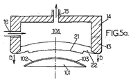
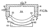
- 指定したパターン(P)に従い、受け側にパターニングをするスタンプであって、静止状態にて平面とされ、かつ前記パターンが複製される弾性ダイアフラム(20)のスタンプ表面(21)を備え、前記ダイアフラムの中間部の点が前記スタンプ表面(21)に直交する方向に沿って、前記剛体部に対して移動可能であるように、前記ダイアフラムは前記ダイアフラムの周縁部に沿って剛体部(13)に取り付けられ、前記スタンプは、前記ダイアフラムが前記中間部よりも前記周縁部付近においてより弾性があることを特徴とする、スタンプ。
- 前記ダイアフラム(20)は、リング状部分(22)に囲まれた中間部よりも、前記周縁部付近の前記リング状部分においてより薄くされている、請求項1に記載のスタンプ。
- 前記ダイアフラム(20)が前記スタンプ表面(21)と直交する方向に沿って積み重ねられた複数の弾性層(A、B)を備え、前記スタンプ表面が前記ダイアフラムの前記層のなかで最も高い硬度を有する前記弾性層(A)を含む、請求項1または2に記載のスタンプ。
- 前記最も高い硬度を有する弾性層(A)が、前記パターン(P)に対応する前記スタンプ表面の少なくとも一つの領域において、50μmと500μmの間の厚さを有する、請求項3に記載のスタンプ。
- 前記ダイアフラム(20)によって境界付けられた、密封された筐体(104)、および前記筐体内の圧力を変化させて、前記スタンプ表面(21)の凹面または凸面を、前記圧力によって制御することができる手段をさらに備える、請求項1から4のいずれか一項に記載のスタンプ。
- 前記弾性ダイアフラムの少なくとも一部がシロキサン型エラストマから形成される、請求項1から5のいずれか一項に記載のスタンプ。
- 前記シロキサン型エラストマが紫外光を透過する、請求項6に記載のスタンプ。
- 前記ダイアフラム(20)は、直径が10mm以上であり、厚さが前記ダイアフラムのスタンプ表面領域において2.5mm以上であり、前記リング状部分(22)において厚さが0.5mmから2.0mmであるディスク状である、請求項2から7のいずれか一項に記載のスタンプ。
- 前記ダイアフラム(20)のリング状部分が、長い直径と短い直径との間に、1mmと10mmの間の差を有する、請求項8に記載のスタンプ。
- モールド底部(1)に、前記モールド底部の平面上に複製されるパターン(P)を提供する工程と、
前記モールドサイド部分の内底端部が前記パターン(P)を囲むように、前記モールドサイド部分(2)を前記モールド底部(1)上に配置する工程であって、前記モールドサイド部分(2)は、下側モールドサイド部分(12)および上側モールドサイド部分(13)を備え、個々の内部ボアは一列に並んでおり、前記モールドサイド部分のうちの一つの前記ボアが他のモールドサイド部分のボアよりも断面においてより大きくされた、工程と、
前記下側モールドサイド部分(12)のボアの高さ(h)よりも高い厚さ(e)を有するエラストマダイアフラム(20)を形成するために重ね合わされた前記モールド底部(1)および前記モールドサイド部分(2)を備える前記モールド(100)に、少なくとも一つのエラストマ前駆物質を注入する工程と、
前記下側モールドサイド部分および前記上側モールドサイド部分のうちの最大のボアに対応する前記ダイアフラム(20)の周縁部に沿って、前記ダイアフラムを剛体部(13)に固定する工程と
を含む、スタンプ製造方法。 - 前記パターン(P)が前記モールド底部(1)の上面に形成される、請求項10に記載のスタンプ製造方法。
- 前記上側モールドサイド部分(13)のボアが前記下側モールドサイド部分(12)のボアよりも大きい、請求項10または11に記載のスタンプ製造方法。
- 前記エラストマ前駆物質を注入する前に、前記最大のボアを有する前記モールドサイド部分の内表面に、前記エラストマの接着促進剤を塗布する工程であって、前記最大のボアを有する前記モールドサイド部分が前記剛体部(13)の一部である、工程をさらに含む、請求項10から12のいずれか一項に記載のスタンプ製造方法。
- 前記最大のボア(13)を有する前記モールドサイド部分は、前記接着促進剤が塗布される内溝(13a)を備えている、請求項13に記載のスタンプ製造方法。
- 前記下側モールドサイド部分(12)および前記上側モールドサイド部分(13)が別個の部分であり、前記下側モールドサイド部分および前記上側モールドサイド部分を一列に結合する手段が提供されている、請求項10から14のいずれか一項に記載のスタンプ製造方法。
- 対象物(101)の擬似球面状をなした受け側表面(103)に印刷されたパターン(P)を有する前記対象物を製造する方法であって、
請求項1から6、または8、または9のいずれか一項に記載のスタンプの前記スタンプ表面(21)にインクを塗布する工程と、
前記対象物の受け側表面(103)に対して、前記スタンプのスタンプ表面(21)を押圧する工程と、
前記対象物から前記スタンプを取り除く工程と、
ウェット・エッチングまたは化学メッキ法によって前記受け側表面を加工する工程と
を含む、方法。 - 対象物(101)の擬似球面状をなした受け側表面(103)に印刷されたパターン(P)を有する前記対象物を製造する方法であって、
凹面のスタンプ表面に光吸収層を積層する工程と、
前記受け側表面にフォトレジストを適用する工程と、
前記対象物の受け側表面(103)に前記スタンプ表面(21)を押圧することによって、光結合マスクとして、請求項1から5または請求項7から9のいずれか一項に記載の前記スタンプを用いる工程であって、前記スタンプを紫外光に曝す、工程と、
前記対象物から前記スタンプを取り除く工程と、
フォトレジストを現像する工程と
を含む、方法。 - 前記受け側表面が55mmより大きい曲率半径を有し、凹面または凸面である、請求項16または17に記載の対象物を製造する方法。
- 前記対象物の前記受け側表面(103)に前記スタンプの前記スタンプ表面(21)を押圧する前に、
前記スタンプ表面(21)および前記受け側表面(103)が相補的形状を有し、かつ前記受け側表面に対して前記スタンプ表面を押圧することが前記スタンプ表面の中間部において接触することによって開始されるように、前記筐体(104)内の圧力を調整する工程
をさらに含む、請求項5または請求項16から18のいずれか一項に記載の対象物を製造する方法。 - 前記スタンプ表面の湾曲は、前記受け側表面(103)に前記スタンプ表面(21)を押圧する間、光学的なモニタリングが行われる、請求項16から19のいずれか一項に記載の対象物を製造する方法。
- 前記インクが、導電層(102)上に自己組織化単分子層を形成するように配合されている、請求項16に記載の対象物を製造する方法。
- 前記インクが触媒分子の溶液である、請求項16に記載の対象物を製造する方法。
- 前記導電層(102)が金属層である、請求項21に記載の対象物を製造する方法。
- 前記金属を、金、銀、パラジウム、プラチナ、アルミニウム、および銅から選択する、請求項23に記載の対象物を製造する方法。
- 前記対象物が光学レンズ(101)からなる、請求項16から24のいずれか一項に記載の対象物を製造する方法。
- 前記光学レンズ(101)が眼科用レンズである、請求項25に記載の対象物を製造する方法。
- 前記パターン(P)が線形状の導電グリッドを含む、請求項25または26に記載の対象物を製造する方法。
- 前記グリッドが0.1μmから0.4μmの範囲内の間隔(p)を有する、請求項27に記載の対象物を製造する方法。
- 前記グリッドの間隔(p)が0.14μmから0.25μmの範囲内である、請求項28に記載の対象物を製造する方法。
- 前記グリッドの厚み(t)が30nm以上の平行な導電ライン(110)を含む、請求項27から29のいずれか一項に記載の対象物を製造する方法。
- グリッドライン(110)の幅(l)が0.15μm以下である、請求項27から30のいずれか一項に記載の対象物を製造する方法。
- 前記グリッドが、前記光学レンズ(101)上に当たる光に少なくとも部分的な偏光効果を生じさせる、請求項27から31のいずれか一項に記載の方法。
- 前記レンズの可視光域における透過率が、前記グリッドライン(110)に対して直交する偏光成分に対して16%から95%の範囲内とされ、かつ前記グリッドラインと平行な偏光成分に対して0%から5%の範囲内とされる、請求項32に記載の方法。
- 対象物(101)の擬似球面状をなした受け側表面(103)に印刷されたパターン(P)を有する前記対象物を製造する方法であって、
前記受け側表面に重合性液体を塗布する工程と、
請求項7に記載のスタンプを用いる工程と、
前記対象物の受け側表面(103)にスタンプ表面(21)を押圧する工程であって、紫外光で液体を硬化させる、工程と、
対象物からスタンプを除去する工程と
を含む、方法。 - 対象物(101)の擬似球面状をなした受け側表面(103)に印刷されたパターン(P)を有する前記対象物を製造する方法であって、
前記スタンプ表面に重合性液体を塗布する工程と、
請求項7に記載のスタンプを用いる工程と、前記対象物の受け側表面(103)にスタンプ表面(21)を押圧する工程であって、紫外光で液体を硬化させる、工程と、
対象物からスタンプを除去する工程と
を含む、方法。 - 対象物(101)の擬似球面状をなした受け側表面(103)に印刷されたパターン(P)を有する前記対象物を製造する方法であって、
前記受け側表面に重合性液体を塗布する工程と、
請求項1から6のいずれか一項に記載のスタンプを用いる工程と、
前記対象物の受け側表面(103)にスタンプ表面(21)を押圧する工程であって、熱硬化で液体を硬化させる、工程と、
対象物からスタンプを除去する工程と
を含む、方法。 - 対象物(101)の擬似球面状をなした受け側表面(103)に印刷されたパターン(P)を有する前記対象物を製造する方法であって、
前記スタンプ表面に重合性液体を塗布する工程と、
請求項1から6のいずれか一項に記載のスタンプを用いる工程と、
前記対象物の受け側表面(103)にスタンプ表面(21)を押圧する工程であって、熱硬化で液体を硬化させる、工程と、
対象物からスタンプを除去する工程と
を含む、方法。
Applications Claiming Priority (2)
| Application Number | Priority Date | Filing Date | Title |
|---|---|---|---|
| EP04292954A EP1669196B1 (en) | 2004-12-10 | 2004-12-10 | Stamp for patterning, method for manufacturing such stamp and method for manufacturing an object using the stamp. |
| PCT/EP2005/013529 WO2006061255A1 (en) | 2004-12-10 | 2005-12-01 | Stamp for patterning, method for manufacturing such stamp and method for manufacturing an object using the stamp |
Publications (1)
| Publication Number | Publication Date |
|---|---|
| JP2008522867A true JP2008522867A (ja) | 2008-07-03 |
Family
ID=34931592
Family Applications (1)
| Application Number | Title | Priority Date | Filing Date |
|---|---|---|---|
| JP2007544845A Pending JP2008522867A (ja) | 2004-12-10 | 2005-12-01 | パターニング用スタンプ、該スタンプの製造方法、および該スタンプを用いて対象物を製造する方法 |
Country Status (6)
| Country | Link |
|---|---|
| US (1) | US8268544B2 (ja) |
| EP (2) | EP1669196B1 (ja) |
| JP (1) | JP2008522867A (ja) |
| AT (1) | ATE396048T1 (ja) |
| DE (1) | DE602004014002D1 (ja) |
| WO (1) | WO2006061255A1 (ja) |
Cited By (2)
| Publication number | Priority date | Publication date | Assignee | Title |
|---|---|---|---|---|
| JP2020088286A (ja) * | 2018-11-29 | 2020-06-04 | キヤノン株式会社 | 成形装置、成形方法、および物品の製造方法 |
| KR102415094B1 (ko) * | 2021-11-17 | 2022-06-30 | 한국기계연구원 | 비평면기판용 나노임프린트 노광장치 및 방법 |
Families Citing this family (22)
| Publication number | Priority date | Publication date | Assignee | Title |
|---|---|---|---|---|
| US20080160129A1 (en) * | 2006-05-11 | 2008-07-03 | Molecular Imprints, Inc. | Template Having a Varying Thickness to Facilitate Expelling a Gas Positioned Between a Substrate and the Template |
| JP5062551B2 (ja) * | 2007-01-30 | 2012-10-31 | 株式会社吉野工業所 | タンポ印刷方法とタンポ印刷用のタンポ転写体 |
| US7678423B2 (en) * | 2007-02-27 | 2010-03-16 | The Regents Of The University Of Michigan | System and method for depositing thin layers on non-planar substrates by stamping |
| US20090020910A1 (en) * | 2007-02-27 | 2009-01-22 | Stephen Forrest | System and method for depositing thin layers on non-planar substrates by stamping |
| ATE484773T1 (de) * | 2007-03-21 | 2010-10-15 | Erich Thallner | Verfahren und vorrichtung zur erzeugung einer nanostrukturierten scheibe |
| DE102007019398A1 (de) * | 2007-04-23 | 2008-11-06 | Itw Morlock Gmbh | Tampondruckmaschine und Tampon dafür |
| DE102008001800A1 (de) | 2007-05-25 | 2008-11-27 | Carl Zeiss Smt Ag | Projektionsobjektiv für die Mikrolithographie, Mikrolithographie-Projektionsbelichtungsanlage mit einem derartigen Projektionsobjektiv, mikrolithographisches Herstellungsverfahren für Bauelemente sowie mit diesem Verfahren hergestelltes Bauelement |
| DE112008001634A5 (de) * | 2007-06-21 | 2010-04-01 | GeSIM Gesellschaft für Silizium-Mikrosysteme mbH | Verfahren und Vorrichtung zur Übertragung von Mikro- oder Nanostrukturen durch Kontaktstempeln |
| US20090025595A1 (en) * | 2007-07-25 | 2009-01-29 | Nano Terra Inc. | Contact Printing Method Using an Elastomeric Stamp Having a Variable Surface Area and Variable Shape |
| WO2009129443A2 (en) * | 2008-04-17 | 2009-10-22 | Massachusetts Institute Of Technology | Diaphragm flexure with large range and high load capacity |
| US9793481B2 (en) * | 2008-10-01 | 2017-10-17 | The Regents Of The University Of Michigan | Patterning by stamped metal resist |
| KR20120034940A (ko) * | 2010-10-04 | 2012-04-13 | 삼성전자주식회사 | 패터닝 몰드 및 그 제조방법 |
| WO2012157636A1 (ja) * | 2011-05-19 | 2012-11-22 | 綜研化学株式会社 | ナノインプリント用モールドおよび曲面体 |
| TW201321214A (zh) * | 2011-11-29 | 2013-06-01 | Wistron Corp | 印壓方法及印壓模具 |
| JP2014226859A (ja) * | 2013-05-23 | 2014-12-08 | 株式会社秀峰 | 印刷方法 |
| US20150108673A1 (en) * | 2013-10-18 | 2015-04-23 | The Chinese University Of Hong Kong | Imprinting apparatus and method for imprinting |
| US10675975B2 (en) * | 2015-04-17 | 2020-06-09 | Visteon Global Technologies, Inc. | Glass lens assembly with an elastic adhesive |
| US11840013B2 (en) * | 2018-02-27 | 2023-12-12 | Matthews International Corporation | Graphite materials and devices with surface micro-texturing |
| CN113167944A (zh) * | 2018-07-23 | 2021-07-23 | 株式会社日立高新技术 | 凹面衍射光栅的制造方法、制造装置以及凹面衍射光栅 |
| CN109656098A (zh) * | 2018-12-04 | 2019-04-19 | 上海安翰医疗技术有限公司 | 纳米压印弹性模板的制作方法、纳米压印弹性模板及组件 |
| DE102021130516A1 (de) * | 2021-11-22 | 2023-05-25 | Tampoprint Gmbh | Verfahren und Vorrichtung zum Bedrucken oder Dekorieren eines Objekts |
| US11717728B1 (en) * | 2022-02-28 | 2023-08-08 | Acushnet Company | Golf ball having markings spaced from a centerline plane |
Citations (6)
| Publication number | Priority date | Publication date | Assignee | Title |
|---|---|---|---|---|
| JPH01232048A (ja) * | 1988-03-12 | 1989-09-18 | Nec Corp | コンタクトプリンタ装置 |
| JPH09240125A (ja) * | 1996-03-04 | 1997-09-16 | Motorola Inc | 物品の面をスタンピングするための装置および方法 |
| DE10028620A1 (de) * | 2000-06-09 | 2001-12-20 | Heinrich Bielmeier | Vorrichtung zum Bedrucken unebener Oberflächen |
| JP2002040202A (ja) * | 2000-07-21 | 2002-02-06 | Seiko Epson Corp | プラスチックレンズの着色方法および装置 |
| JP2003086537A (ja) * | 2001-09-13 | 2003-03-20 | Tdk Corp | 構造体を用いた薄膜パターン製造方法および構造体 |
| WO2003099463A2 (en) * | 2002-05-27 | 2003-12-04 | Koninklijke Philips Electronics N.V. | Method and device for transferring a pattern from a stamp to a substrate |
Family Cites Families (22)
| Publication number | Priority date | Publication date | Assignee | Title |
|---|---|---|---|---|
| US2748696A (en) * | 1951-06-13 | 1956-06-05 | Murray Lilian | Printing or decoration of ceramic or other ware |
| US4508031A (en) * | 1981-12-21 | 1985-04-02 | Corning Glass Works | Flexible membrane printing apparatus for a decorating machine |
| US6180239B1 (en) * | 1993-10-04 | 2001-01-30 | President And Fellows Of Harvard College | Microcontact printing on surfaces and derivative articles |
| EP0812434B1 (en) | 1995-03-01 | 2013-09-18 | President and Fellows of Harvard College | Microcontact printing on surfaces and derivative articles |
| US5804017A (en) * | 1995-07-27 | 1998-09-08 | Imation Corp. | Method and apparatus for making an optical information record |
| JP3372258B2 (ja) * | 1995-08-04 | 2003-01-27 | インターナシヨナル・ビジネス・マシーンズ・コーポレーシヨン | リソグラフィ・プロセス用のスタンプ |
| EP0784543B1 (en) * | 1995-08-04 | 2000-04-26 | International Business Machines Corporation | Lithographic surface or thin layer modification |
| US6060121A (en) | 1996-03-15 | 2000-05-09 | President And Fellows Of Harvard College | Microcontact printing of catalytic colloids |
| US6096386A (en) * | 1996-09-06 | 2000-08-01 | International Business Machines Corporation | Method of oriented depositing chemically defined bodies |
| US5948621A (en) * | 1997-09-30 | 1999-09-07 | The United States Of America As Represented By The Secretary Of The Navy | Direct molecular patterning using a micro-stamp gel |
| US5937758A (en) | 1997-11-26 | 1999-08-17 | Motorola, Inc. | Micro-contact printing stamp |
| US6871951B2 (en) * | 2000-06-23 | 2005-03-29 | E-Vision, Llc | Electro-optic lens with integrated components |
| US6517995B1 (en) * | 1999-09-14 | 2003-02-11 | Massachusetts Institute Of Technology | Fabrication of finely featured devices by liquid embossing |
| TW562755B (en) * | 1999-12-31 | 2003-11-21 | Ibm | Stamp device for printing a pattern on a surface of a substrate |
| US6542307B2 (en) * | 2000-10-20 | 2003-04-01 | Three-Five Systems, Inc. | Compact near-eye illumination system |
| US7338613B2 (en) * | 2001-09-10 | 2008-03-04 | Surface Logix, Inc. | System and process for automated microcontact printing |
| WO2003065120A2 (en) * | 2002-01-11 | 2003-08-07 | Massachusetts Institute Of Technology | Microcontact printing |
| US6656308B2 (en) * | 2002-04-22 | 2003-12-02 | International Business Machines Corporation | Process of fabricating a precision microcontact printing stamp |
| US6792856B2 (en) | 2002-07-16 | 2004-09-21 | International Business Machines Corporation | Method and apparatus for accurate, micro-contact printing |
| US20040046927A1 (en) * | 2002-08-27 | 2004-03-11 | Montgomery Mark E. | Polarized and non-polarized bifocal spectacles |
| US6981445B2 (en) * | 2003-12-24 | 2006-01-03 | Axela Biosensors Inc. | Method and apparatus for micro-contact printing |
| DE102005028704B4 (de) * | 2005-06-20 | 2016-09-08 | Infineon Technologies Ag | Verfahren zur Herstellung eines Halbleiterbauteils mit in Kunststoffgehäusemasse eingebetteten Halbleiterbauteilkomponenten |
-
2004
- 2004-12-10 AT AT04292954T patent/ATE396048T1/de not_active IP Right Cessation
- 2004-12-10 EP EP04292954A patent/EP1669196B1/en active Active
- 2004-12-10 DE DE602004014002T patent/DE602004014002D1/de active Active
-
2005
- 2005-12-01 US US11/721,199 patent/US8268544B2/en active Active
- 2005-12-01 WO PCT/EP2005/013529 patent/WO2006061255A1/en active Application Filing
- 2005-12-01 JP JP2007544845A patent/JP2008522867A/ja active Pending
- 2005-12-01 EP EP05824198A patent/EP1819514A1/en not_active Withdrawn
Patent Citations (6)
| Publication number | Priority date | Publication date | Assignee | Title |
|---|---|---|---|---|
| JPH01232048A (ja) * | 1988-03-12 | 1989-09-18 | Nec Corp | コンタクトプリンタ装置 |
| JPH09240125A (ja) * | 1996-03-04 | 1997-09-16 | Motorola Inc | 物品の面をスタンピングするための装置および方法 |
| DE10028620A1 (de) * | 2000-06-09 | 2001-12-20 | Heinrich Bielmeier | Vorrichtung zum Bedrucken unebener Oberflächen |
| JP2002040202A (ja) * | 2000-07-21 | 2002-02-06 | Seiko Epson Corp | プラスチックレンズの着色方法および装置 |
| JP2003086537A (ja) * | 2001-09-13 | 2003-03-20 | Tdk Corp | 構造体を用いた薄膜パターン製造方法および構造体 |
| WO2003099463A2 (en) * | 2002-05-27 | 2003-12-04 | Koninklijke Philips Electronics N.V. | Method and device for transferring a pattern from a stamp to a substrate |
Cited By (3)
| Publication number | Priority date | Publication date | Assignee | Title |
|---|---|---|---|---|
| JP2020088286A (ja) * | 2018-11-29 | 2020-06-04 | キヤノン株式会社 | 成形装置、成形方法、および物品の製造方法 |
| JP7171394B2 (ja) | 2018-11-29 | 2022-11-15 | キヤノン株式会社 | 成形装置、成形方法、および物品の製造方法 |
| KR102415094B1 (ko) * | 2021-11-17 | 2022-06-30 | 한국기계연구원 | 비평면기판용 나노임프린트 노광장치 및 방법 |
Also Published As
| Publication number | Publication date |
|---|---|
| DE602004014002D1 (de) | 2008-07-03 |
| EP1819514A1 (en) | 2007-08-22 |
| EP1669196A1 (en) | 2006-06-14 |
| US8268544B2 (en) | 2012-09-18 |
| US20090208882A1 (en) | 2009-08-20 |
| WO2006061255A1 (en) | 2006-06-15 |
| ATE396048T1 (de) | 2008-06-15 |
| EP1669196B1 (en) | 2008-05-21 |
Similar Documents
| Publication | Publication Date | Title |
|---|---|---|
| JP2008522867A (ja) | パターニング用スタンプ、該スタンプの製造方法、および該スタンプを用いて対象物を製造する方法 | |
| JP5225618B2 (ja) | ナノインプリント用モールド及びその製造方法 | |
| JP6173354B2 (ja) | 光透過型インプリント用モールド、大面積モールドの製造方法 | |
| US7632087B2 (en) | Composite stamper for imprint lithography | |
| JP5411557B2 (ja) | 微細構造転写装置 | |
| WO2016006592A1 (ja) | ステップアンドリピート用インプリント用モールド及びその製造方法 | |
| JP5633744B2 (ja) | 基材作製方法、ナノインプリントリソグラフィ方法及び型複製方法 | |
| JP4448868B2 (ja) | インプリント用スタンパとその製造方法 | |
| TWI576229B (zh) | 奈米壓印之安全分離技術 | |
| JP5761320B2 (ja) | マイクロコンタクトプリンティング用スタンプの製造方法 | |
| KR100889814B1 (ko) | 스탬퍼 및 그 제조방법과 스탬퍼를 이용한 기판의 임프린팅공정 | |
| US9180608B2 (en) | Stamp, method of manufacturing the same, and imprinting method using the stamp | |
| KR101542942B1 (ko) | 플라즈모닉 특성제어를 위한 금속나노패턴 형성방법 | |
| KR20110140059A (ko) | 나노 임프린트용 스탬프 및 이의 제조 방법 | |
| JP5428449B2 (ja) | マイクロコンタクトプリンティング用スタンプ作製用マスター版の製造方法、およびマイクロコンタクトプリンティング用スタンプ作製用マスター版 | |
| KR102415094B1 (ko) | 비평면기판용 나노임프린트 노광장치 및 방법 | |
| KR101977122B1 (ko) | 나노몰드 및 그 제조방법 | |
| KR101993385B1 (ko) | 스탬프의 제조 방법 | |
| JPWO2020080372A1 (ja) | 微細パターン成形方法、インプリント用モールド製造方法およびインプリント用モールド並びに光学デバイス | |
| KR20090102994A (ko) | 임프린팅 장치의 롤러 구조 |
Legal Events
| Date | Code | Title | Description |
|---|---|---|---|
| A621 | Written request for application examination |
Free format text: JAPANESE INTERMEDIATE CODE: A621 Effective date: 20080815 |
|
| A131 | Notification of reasons for refusal |
Free format text: JAPANESE INTERMEDIATE CODE: A131 Effective date: 20110426 |
|
| A601 | Written request for extension of time |
Free format text: JAPANESE INTERMEDIATE CODE: A601 Effective date: 20110705 |
|
| A602 | Written permission of extension of time |
Free format text: JAPANESE INTERMEDIATE CODE: A602 Effective date: 20110712 |
|
| A02 | Decision of refusal |
Free format text: JAPANESE INTERMEDIATE CODE: A02 Effective date: 20111108 |