JP2008522867A - Patterning stamp, method for manufacturing the stamp, and method for manufacturing an object using the stamp - Google Patents
Patterning stamp, method for manufacturing the stamp, and method for manufacturing an object using the stamp Download PDFInfo
- Publication number
- JP2008522867A JP2008522867A JP2007544845A JP2007544845A JP2008522867A JP 2008522867 A JP2008522867 A JP 2008522867A JP 2007544845 A JP2007544845 A JP 2007544845A JP 2007544845 A JP2007544845 A JP 2007544845A JP 2008522867 A JP2008522867 A JP 2008522867A
- Authority
- JP
- Japan
- Prior art keywords
- stamp
- manufacturing
- diaphragm
- receiving surface
- pattern
- Prior art date
- Legal status (The legal status is an assumption and is not a legal conclusion. Google has not performed a legal analysis and makes no representation as to the accuracy of the status listed.)
- Pending
Links
Images


Classifications
-
- B—PERFORMING OPERATIONS; TRANSPORTING
- B41—PRINTING; LINING MACHINES; TYPEWRITERS; STAMPS
- B41F—PRINTING MACHINES OR PRESSES
- B41F17/00—Printing apparatus or machines of special types or for particular purposes, not otherwise provided for
- B41F17/001—Pad printing apparatus or machines
-
- B—PERFORMING OPERATIONS; TRANSPORTING
- B29—WORKING OF PLASTICS; WORKING OF SUBSTANCES IN A PLASTIC STATE IN GENERAL
- B29C—SHAPING OR JOINING OF PLASTICS; SHAPING OF MATERIAL IN A PLASTIC STATE, NOT OTHERWISE PROVIDED FOR; AFTER-TREATMENT OF THE SHAPED PRODUCTS, e.g. REPAIRING
- B29C43/00—Compression moulding, i.e. applying external pressure to flow the moulding material; Apparatus therefor
- B29C43/003—Compression moulding, i.e. applying external pressure to flow the moulding material; Apparatus therefor characterised by the choice of material
-
- B—PERFORMING OPERATIONS; TRANSPORTING
- B29—WORKING OF PLASTICS; WORKING OF SUBSTANCES IN A PLASTIC STATE IN GENERAL
- B29C—SHAPING OR JOINING OF PLASTICS; SHAPING OF MATERIAL IN A PLASTIC STATE, NOT OTHERWISE PROVIDED FOR; AFTER-TREATMENT OF THE SHAPED PRODUCTS, e.g. REPAIRING
- B29C43/00—Compression moulding, i.e. applying external pressure to flow the moulding material; Apparatus therefor
- B29C43/02—Compression moulding, i.e. applying external pressure to flow the moulding material; Apparatus therefor of articles of definite length, i.e. discrete articles
- B29C43/021—Compression moulding, i.e. applying external pressure to flow the moulding material; Apparatus therefor of articles of definite length, i.e. discrete articles characterised by the shape of the surface
-
- B—PERFORMING OPERATIONS; TRANSPORTING
- B29—WORKING OF PLASTICS; WORKING OF SUBSTANCES IN A PLASTIC STATE IN GENERAL
- B29C—SHAPING OR JOINING OF PLASTICS; SHAPING OF MATERIAL IN A PLASTIC STATE, NOT OTHERWISE PROVIDED FOR; AFTER-TREATMENT OF THE SHAPED PRODUCTS, e.g. REPAIRING
- B29C43/00—Compression moulding, i.e. applying external pressure to flow the moulding material; Apparatus therefor
- B29C43/02—Compression moulding, i.e. applying external pressure to flow the moulding material; Apparatus therefor of articles of definite length, i.e. discrete articles
- B29C43/10—Isostatic pressing, i.e. using non-rigid pressure-exerting members against rigid parts or dies
- B29C43/12—Isostatic pressing, i.e. using non-rigid pressure-exerting members against rigid parts or dies using bags surrounding the moulding material or using membranes contacting the moulding material
-
- B—PERFORMING OPERATIONS; TRANSPORTING
- B29—WORKING OF PLASTICS; WORKING OF SUBSTANCES IN A PLASTIC STATE IN GENERAL
- B29C—SHAPING OR JOINING OF PLASTICS; SHAPING OF MATERIAL IN A PLASTIC STATE, NOT OTHERWISE PROVIDED FOR; AFTER-TREATMENT OF THE SHAPED PRODUCTS, e.g. REPAIRING
- B29C59/00—Surface shaping of articles, e.g. embossing; Apparatus therefor
- B29C59/02—Surface shaping of articles, e.g. embossing; Apparatus therefor by mechanical means, e.g. pressing
- B29C59/021—Surface shaping of articles, e.g. embossing; Apparatus therefor by mechanical means, e.g. pressing of profiled articles, e.g. hollow or tubular articles, beams
-
- B—PERFORMING OPERATIONS; TRANSPORTING
- B29—WORKING OF PLASTICS; WORKING OF SUBSTANCES IN A PLASTIC STATE IN GENERAL
- B29C—SHAPING OR JOINING OF PLASTICS; SHAPING OF MATERIAL IN A PLASTIC STATE, NOT OTHERWISE PROVIDED FOR; AFTER-TREATMENT OF THE SHAPED PRODUCTS, e.g. REPAIRING
- B29C59/00—Surface shaping of articles, e.g. embossing; Apparatus therefor
- B29C59/02—Surface shaping of articles, e.g. embossing; Apparatus therefor by mechanical means, e.g. pressing
- B29C59/026—Surface shaping of articles, e.g. embossing; Apparatus therefor by mechanical means, e.g. pressing of layered or coated substantially flat surfaces
-
- B—PERFORMING OPERATIONS; TRANSPORTING
- B41—PRINTING; LINING MACHINES; TYPEWRITERS; STAMPS
- B41F—PRINTING MACHINES OR PRESSES
- B41F17/00—Printing apparatus or machines of special types or for particular purposes, not otherwise provided for
- B41F17/30—Printing apparatus or machines of special types or for particular purposes, not otherwise provided for for printing on curved surfaces of essentially spherical, or part-spherical, articles
-
- B—PERFORMING OPERATIONS; TRANSPORTING
- B82—NANOTECHNOLOGY
- B82Y—SPECIFIC USES OR APPLICATIONS OF NANOSTRUCTURES; MEASUREMENT OR ANALYSIS OF NANOSTRUCTURES; MANUFACTURE OR TREATMENT OF NANOSTRUCTURES
- B82Y10/00—Nanotechnology for information processing, storage or transmission, e.g. quantum computing or single electron logic
-
- B—PERFORMING OPERATIONS; TRANSPORTING
- B82—NANOTECHNOLOGY
- B82Y—SPECIFIC USES OR APPLICATIONS OF NANOSTRUCTURES; MEASUREMENT OR ANALYSIS OF NANOSTRUCTURES; MANUFACTURE OR TREATMENT OF NANOSTRUCTURES
- B82Y30/00—Nanotechnology for materials or surface science, e.g. nanocomposites
-
- B—PERFORMING OPERATIONS; TRANSPORTING
- B82—NANOTECHNOLOGY
- B82Y—SPECIFIC USES OR APPLICATIONS OF NANOSTRUCTURES; MEASUREMENT OR ANALYSIS OF NANOSTRUCTURES; MANUFACTURE OR TREATMENT OF NANOSTRUCTURES
- B82Y40/00—Manufacture or treatment of nanostructures
-
- G—PHYSICS
- G03—PHOTOGRAPHY; CINEMATOGRAPHY; ANALOGOUS TECHNIQUES USING WAVES OTHER THAN OPTICAL WAVES; ELECTROGRAPHY; HOLOGRAPHY
- G03F—PHOTOMECHANICAL PRODUCTION OF TEXTURED OR PATTERNED SURFACES, e.g. FOR PRINTING, FOR PROCESSING OF SEMICONDUCTOR DEVICES; MATERIALS THEREFOR; ORIGINALS THEREFOR; APPARATUS SPECIALLY ADAPTED THEREFOR
- G03F7/00—Photomechanical, e.g. photolithographic, production of textured or patterned surfaces, e.g. printing surfaces; Materials therefor, e.g. comprising photoresists; Apparatus specially adapted therefor
- G03F7/0002—Lithographic processes using patterning methods other than those involving the exposure to radiation, e.g. by stamping
-
- B—PERFORMING OPERATIONS; TRANSPORTING
- B29—WORKING OF PLASTICS; WORKING OF SUBSTANCES IN A PLASTIC STATE IN GENERAL
- B29C—SHAPING OR JOINING OF PLASTICS; SHAPING OF MATERIAL IN A PLASTIC STATE, NOT OTHERWISE PROVIDED FOR; AFTER-TREATMENT OF THE SHAPED PRODUCTS, e.g. REPAIRING
- B29C35/00—Heating, cooling or curing, e.g. crosslinking or vulcanising; Apparatus therefor
- B29C35/02—Heating or curing, e.g. crosslinking or vulcanizing during moulding, e.g. in a mould
- B29C35/08—Heating or curing, e.g. crosslinking or vulcanizing during moulding, e.g. in a mould by wave energy or particle radiation
- B29C35/0805—Heating or curing, e.g. crosslinking or vulcanizing during moulding, e.g. in a mould by wave energy or particle radiation using electromagnetic radiation
- B29C2035/0827—Heating or curing, e.g. crosslinking or vulcanizing during moulding, e.g. in a mould by wave energy or particle radiation using electromagnetic radiation using UV radiation
-
- B—PERFORMING OPERATIONS; TRANSPORTING
- B29—WORKING OF PLASTICS; WORKING OF SUBSTANCES IN A PLASTIC STATE IN GENERAL
- B29C—SHAPING OR JOINING OF PLASTICS; SHAPING OF MATERIAL IN A PLASTIC STATE, NOT OTHERWISE PROVIDED FOR; AFTER-TREATMENT OF THE SHAPED PRODUCTS, e.g. REPAIRING
- B29C43/00—Compression moulding, i.e. applying external pressure to flow the moulding material; Apparatus therefor
- B29C43/02—Compression moulding, i.e. applying external pressure to flow the moulding material; Apparatus therefor of articles of definite length, i.e. discrete articles
- B29C43/021—Compression moulding, i.e. applying external pressure to flow the moulding material; Apparatus therefor of articles of definite length, i.e. discrete articles characterised by the shape of the surface
- B29C2043/023—Compression moulding, i.e. applying external pressure to flow the moulding material; Apparatus therefor of articles of definite length, i.e. discrete articles characterised by the shape of the surface having a plurality of grooves
- B29C2043/025—Compression moulding, i.e. applying external pressure to flow the moulding material; Apparatus therefor of articles of definite length, i.e. discrete articles characterised by the shape of the surface having a plurality of grooves forming a microstructure, i.e. fine patterning
-
- B—PERFORMING OPERATIONS; TRANSPORTING
- B29—WORKING OF PLASTICS; WORKING OF SUBSTANCES IN A PLASTIC STATE IN GENERAL
- B29C—SHAPING OR JOINING OF PLASTICS; SHAPING OF MATERIAL IN A PLASTIC STATE, NOT OTHERWISE PROVIDED FOR; AFTER-TREATMENT OF THE SHAPED PRODUCTS, e.g. REPAIRING
- B29C43/00—Compression moulding, i.e. applying external pressure to flow the moulding material; Apparatus therefor
- B29C43/32—Component parts, details or accessories; Auxiliary operations
- B29C43/36—Moulds for making articles of definite length, i.e. discrete articles
- B29C43/3642—Bags, bleeder sheets or cauls for isostatic pressing
- B29C2043/3647—Membranes, diaphragms
-
- B—PERFORMING OPERATIONS; TRANSPORTING
- B29—WORKING OF PLASTICS; WORKING OF SUBSTANCES IN A PLASTIC STATE IN GENERAL
- B29C—SHAPING OR JOINING OF PLASTICS; SHAPING OF MATERIAL IN A PLASTIC STATE, NOT OTHERWISE PROVIDED FOR; AFTER-TREATMENT OF THE SHAPED PRODUCTS, e.g. REPAIRING
- B29C59/00—Surface shaping of articles, e.g. embossing; Apparatus therefor
- B29C59/02—Surface shaping of articles, e.g. embossing; Apparatus therefor by mechanical means, e.g. pressing
- B29C59/022—Surface shaping of articles, e.g. embossing; Apparatus therefor by mechanical means, e.g. pressing characterised by the disposition or the configuration, e.g. dimensions, of the embossments or the shaping tools therefor
- B29C2059/023—Microembossing
Landscapes
- Engineering & Computer Science (AREA)
- Chemical & Material Sciences (AREA)
- Nanotechnology (AREA)
- Mechanical Engineering (AREA)
- Physics & Mathematics (AREA)
- Crystallography & Structural Chemistry (AREA)
- General Physics & Mathematics (AREA)
- Condensed Matter Physics & Semiconductors (AREA)
- Composite Materials (AREA)
- Materials Engineering (AREA)
- Manufacturing & Machinery (AREA)
- Mathematical Physics (AREA)
- Theoretical Computer Science (AREA)
- Shaping Of Tube Ends By Bending Or Straightening (AREA)
- Manufacture Or Reproduction Of Printing Formes (AREA)
- Printing Methods (AREA)
- Application Of Or Painting With Fluid Materials (AREA)
- Nitrogen And Oxygen Or Sulfur-Condensed Heterocyclic Ring Systems (AREA)
Abstract
Description
本発明は受け側表面をパターニングするスタンプおよびそのスタンプの製造方法に関する。本発明はまた、本発明に従ったスタンプを用いることによって実行される印刷工程を有する、対象物を製造する方法に関する。 The present invention relates to a stamp for patterning a receiving surface and a method for manufacturing the stamp. The invention also relates to a method for producing an object, which comprises a printing process carried out by using a stamp according to the invention.
ソフトリソグラフィおよび特にマイクロコンタクト印刷は、迅速かつ低コストでパターンを複製する公知の方法であり、その複製精度は0.50μm(マイクロメートル)よりも高くできる。本方法は、インクをパターンに従ってスタンプ表面から受け側表面へと転写するように、受け側表面に対してインクを染み込ませたスタンプのスタンプ表面を押圧することである。 Soft lithography and in particular microcontact printing are known methods for replicating patterns quickly and at low cost, the replication accuracy of which can be higher than 0.50 μm (micrometers). The method is to press the stamp surface of the stamp soaked with ink against the receiving surface so that the ink is transferred from the stamp surface to the receiving surface according to the pattern.
特許文献1および特許文献2は、大きなパターン印刷を達成するマイクロコンタクト印刷方法の改良を開示している。しかし、これらの改良された方法は球面上または擬似球面上への印刷には使用できない。本発明の範囲において、擬似球面とは連続平面を意味し(すなわち、段差や隙間のない)、凸面または凹面である。また、球面とは、二つの互いに直交する方向に沿った表面の曲率半径が等しい特別な場合である。それゆえ、本明細書で用いる擬似球面という表現には、球面である場合を含めている。
Patent Document 1 and
非特許文献1は、平面でない表面上へのマイクロコンタクト印刷について報告している。しかし、その文献に記載されている方法は、擬似球面状をなした受け側表面には適さない。 Non-Patent Document 1 reports on microcontact printing on a non-planar surface. However, the method described in that document is not suitable for a receiving surface having a pseudo-spherical shape.
最後に、特許文献3は、スタンプ表面が凸面であるスタンプを開示している。そのスタンプ表面は、受け側に対して徐々に平らになるのに対して、スタンプ表面の周辺は固定して保持される。スタンプ表面と受け側との間におけるそのような漸近的な接触によって、気泡のトラッピングが回避され、また、そのような接触には、擬似球面状をなした受け側表面が用いられる。しかしこの方法は、受け側表面に塗布する間に、スタンプ表面にて生成される歪み分布が一様でないために、歪んだパターン印刷を生成する。
それゆえ、本発明の目的は、擬似球面の形状をなした受け側に用いられるパターンを印刷するためのスタンプを提供することである。 Therefore, an object of the present invention is to provide a stamp for printing a pattern used on a receiving side having a pseudo-spherical shape.
したがって、本発明は、指定されたパターンに従い、受け側にパターニングをするスタンプを提供し、そのスタンプは、パターンが複製される弾性ダイアフラムのスタンプ表面を備える。スタンプ表面は静止状態にて平面とされるか、または印刷される特定の基板に適合する形状をもつことができる。ダイアフラムの中間部の点がスタンプ表面に直交する方向に沿って、剛体部に対して移動可能であるように、ダイアフラムはダイアフラムの周縁部に沿って剛体部に取り付けられる。さらに、ダイアフラムは中間部よりも周縁部付近において、さらに弾性が高い。本発明との関連において、「スタンプ表面に直交する方向に沿った移動」、つまりスタンプ表面の中心点を通過する法線に対して平行な軸に沿ったダイアフラムの移動は、±20°の角度許容値を有するものとして理解される。 Accordingly, the present invention provides a stamp that is patterned on the receiving side according to a specified pattern, the stamp comprising an elastic diaphragm stamp surface on which the pattern is replicated. The stamp surface can be flat at rest or can have a shape that fits the particular substrate to be printed. The diaphragm is attached to the rigid body along the periphery of the diaphragm so that the point at the middle of the diaphragm is movable relative to the rigid body along a direction perpendicular to the stamp surface. Further, the diaphragm is more elastic in the vicinity of the peripheral portion than in the intermediate portion. In the context of the present invention, “movement along a direction perpendicular to the stamp surface”, ie the movement of the diaphragm along an axis parallel to the normal passing through the center point of the stamp surface is an angle of ± 20 °. It is understood as having a tolerance.
弾性ダイアフラムは、本発明によるスタンプのスタンプ表面を形成するので、そのスタンプ表面が受け側表面に押圧される場合、その受け側の形状に適合するように、スタンプ表面の形状が変化し得る。そして、スタンプは、擬似球面状をなした受け側表面にパターンを印刷するために使用可能である。 The elastic diaphragm forms the stamp surface of the stamp according to the invention, so that when the stamp surface is pressed against the receiving surface, the shape of the stamp surface can change to match the shape of the receiving side. The stamp can be used to print a pattern on the receiving surface having a pseudo-spherical shape.
スタンプのスタンプ表面の形状におけるそのような変化は、特に、曲率半径の小さい受け側表面に対して、パターンの歪みを誘発するおそれがある。しかし、このような歪みは、より弾性のあるダイアフラムの周縁部を提供することによって制限される。実際には、ダイアフラムの湾曲は、ダイアフラムの最も弾性を有する周縁部に主に位置するので、ダイアフラムの中心部分におけるパターンは、受け側にスタンプ表面を押圧する間、ほんの僅かに歪むのみである。したがって、パターンについては、擬似球面状をなした受け側表面に高精度で印刷することが可能となる。 Such a change in the shape of the stamp surface of the stamp can induce pattern distortion, especially for a receiving surface with a small radius of curvature. However, such distortion is limited by providing a more elastic diaphragm periphery. In practice, the curvature of the diaphragm is mainly located at the most elastic peripheral edge of the diaphragm, so that the pattern in the central part of the diaphragm is only slightly distorted while pressing the stamp surface against the receiving side. Therefore, the pattern can be printed with high accuracy on the receiving surface having a pseudo-spherical shape.
本発明の好適な実施形態に従い、周縁部付近のダイアフラムのより高い弾性は、この領域内のダイアフラムの厚さを薄くすることによって得られる。このように、ダイアフラムは、リング状部分に囲まれた中間部に比して、周縁部付近のリング状部分においてより薄い。周縁部と中間部との間におけるダイアフラムの弾性を異ならせるこの方法は簡単であり、スタンプの製造時において容易に実施可能である。さらに、周縁部と中間部との間のダイアフラムの弾性における変更が、スタンプの製造時に一度決定されてしまえば、受け側の印刷中、もはや制御の必要がない。 In accordance with a preferred embodiment of the present invention, higher elasticity of the diaphragm near the periphery is obtained by reducing the thickness of the diaphragm in this region. Thus, the diaphragm is thinner in the ring-shaped part near the peripheral part than in the intermediate part surrounded by the ring-shaped part. This method of varying the elasticity of the diaphragm between the periphery and the middle is simple and can be easily implemented during the manufacture of the stamp. Furthermore, once the change in diaphragm elasticity between the peripheral and intermediate portions is determined once during the manufacture of the stamp, it no longer needs to be controlled during printing on the receiving side.
本発明の別の実施形態によると、ダイアフラムはスタンプ表面と直交する方向に沿って積み重ねられたいくつかの弾性層を備え、スタンプ表面はダイアフラムの層のなかで最も硬度を有する弾性層を含む。したがって、パターンは、擬似球面状をなした受け側表面に印刷される場合、歪みがより小さくなる。ダイアフラムの二層構造は高解像度印刷に特に適している。 According to another embodiment of the invention, the diaphragm comprises a number of elastic layers stacked along a direction orthogonal to the stamp surface, the stamp surface including the most rigid elastic layer of the diaphragm layers. Thus, the pattern is less distorted when printed on the receiving surface having a pseudo-spherical shape. The two-layer structure of the diaphragm is particularly suitable for high resolution printing.
上述したスタンプは凸面である受け側表面に適合する。この場合、受け側表面にスタンプ表面を押圧すると、ダイアフラムと受け側との間の接触はスタンプの中間部で始まり、次いで半径方向に及んでいく。発明者らは、この動作が受け側のパターン印刷の歪みを減らすことを見出した。 The above-described stamp fits a receiving surface that is convex. In this case, when the stamp surface is pressed against the receiving surface, contact between the diaphragm and the receiving side begins at the middle of the stamp and then extends radially. The inventors have found that this action reduces the distortion of pattern printing on the receiving side.
本発明によるスタンプはまた、凹面の受け側表面に適合し得る。この目的のために、スタンプはまた、ダイアフラムによって境界付けられた、密封された筐体、および筐体内の圧力を変化させて、スタンプ表面の凹面または凸面を、圧力により制御することができる手段をさらに備える。次いで、スタンプ表面の形状を、受け側表面の形状に従い、印刷前に設定することが可能である。スタンプ表面の形状のそのような初期設定は、凹面の受け側表面に対して有用であるが、それはまた、凸面の受け側表面に対するパターン印刷精度を改善できる。筐体内の圧力は、凹面の表面への印刷の場合に高くなり、その結果、スタンプ表面と受け側表面との間における最初の接触は、スタンプのほぼ中心部分にて生じる。凸面の受け側表面の場合には、筐体内の圧力を高くすることもできるが、好ましくは、受け側表面への適用の間、ダイアフラムの歪みを減らすために、圧力を減少させる。その結果、パターン印刷の歪みは少なくなる。 The stamp according to the invention can also be adapted to a concave receiving surface. For this purpose, the stamp also has a sealed housing bounded by a diaphragm, and a means by which the pressure within the housing can be varied to control the concave or convex surface of the stamp surface by pressure. Further prepare. It is then possible to set the shape of the stamp surface according to the shape of the receiving surface before printing. Such an initial setting of the shape of the stamp surface is useful for concave receiver surfaces, but it can also improve pattern printing accuracy for convex receiver surfaces. The pressure in the housing is high when printing on a concave surface, so that the initial contact between the stamp surface and the receiving surface occurs at approximately the central portion of the stamp. In the case of a convex receiving surface, the pressure in the housing can be increased, but preferably the pressure is reduced to reduce diaphragm distortion during application to the receiving surface. As a result, pattern printing distortion is reduced.
本発明はまた、そのようなスタンプの製造方法を提供し、モールド底部に、モールド底部の平面上に複製されるパターンを提供する工程と、モールドサイド部分の内底端部がパターンを囲むように、モールドサイド部分をモールド底部に配置する工程であって、モールドサイド部分は、下側モールドサイド部分および上側モールドサイド部分を備え、個々の内部ボアは一列に並んでおり、モールドサイド部分のうちの一つのボアが他方のモールドサイド部分のボアよりも断面においてより大きくされた、工程と、底サイド部のボアの高さよりも高い厚さを有するエラストマダイアフラムを形成するために重ね合わされたモールド底部およびモールドサイド部分を備えるモールドに、少なくとも一つのエラストマ前駆物質を注入する工程と、下側モールドサイド部分および上側モールドサイド部分のうちの最大のボアに対応するダイアフラムの周縁部に沿って、ダイアフラムを剛体部に固定する工程とを含む。 The present invention also provides a method of manufacturing such a stamp, providing a pattern at the bottom of the mold that is replicated on the mold bottom plane, such that the inner bottom edge of the mold side portion surrounds the pattern. , A step of disposing the mold side portion at the bottom of the mold, wherein the mold side portion includes a lower mold side portion and an upper mold side portion, and the individual internal bores are arranged in a line, A mold bottom overlapped to form an elastomer diaphragm having a thickness greater than the height of the bottom side bore, with one bore made larger in cross-section than the other mold side portion bore; Injecting at least one elastomer precursor into a mold having a mold side portion; Along the periphery of the diaphragm corresponding to the largest bore of the mold side parts and upper mold side parts, and a step of fixing the diaphragm to the rigid part.
そのようなスタンプ製造方法は容易および安価である。その理由は、任意の複雑な技術的手段を必要としないからである。さらに、シリコン・ウエハ・リソグラフィなどの公知の技術もまた、モールド底部の上にパターンを複製するのに用いられる。なぜならば、スタンプ表面は静止状態にて平面となるように設計されているからである。 Such a stamp manufacturing method is easy and inexpensive. The reason is that it does not require any complicated technical means. In addition, known techniques such as silicon wafer lithography are also used to replicate the pattern on the mold bottom. This is because the stamp surface is designed to be flat in a stationary state.
好適には、上側モールドサイド部分のボアは下側モールドサイド部分よりも大きい。 Preferably, the upper mold side portion has a larger bore than the lower mold side portion.
より一層の扱い易さのために、下側モールドサイド部分および上側モールドサイド部分は別個の部分であり、下側モールドサイド部分および上側モールドサイド部分を一列に結合する手段が提供されている。 For greater ease of handling, the lower mold side part and the upper mold side part are separate parts, and means are provided for joining the lower mold side part and the upper mold side part in a row.
スタンプ製造方法の好適な実施に従い、エラストマ前駆物質を注入する前に、最大のボアを有するモールドサイド部分の内表面に、エラストマの接着促進剤を塗布する工程をさらに含む。 In accordance with a preferred implementation of the stamp manufacturing method, the method further includes the step of applying an elastomer adhesion promoter to the inner surface of the mold side portion having the largest bore before injecting the elastomer precursor.
また、最大のボアを有するモールドサイド部分はスタンプの剛体部の一部である。それゆえ、ダイアフラムが剛体部に直接、取り付けられて形成されると、スタンプの製造は大幅に簡略化される。これはダイアフラムを剛体部に固定する、別個の製造工程を回避する。なお、そのような固定する工程は、ダイアフラムの恒常的な湾曲によって、パターンの歪みを誘発し得る。 Also, the mold side portion having the largest bore is a part of the rigid portion of the stamp. Therefore, if the diaphragm is formed directly attached to the rigid body, the manufacture of the stamp is greatly simplified. This avoids a separate manufacturing process that secures the diaphragm to the rigid body. Note that such a fixing step can induce distortion of the pattern due to the permanent curvature of the diaphragm.
有利には、最大のボアを有するモールドサイド部分は、接着促進剤が塗布される内溝を備える。したがって、接着促進剤の塗布は、均一に達成されるように、さらに容易に実行される。その結果、ダイアフラムは剛体部にほぼ均等に取り付けられ、パターン印刷の歪みが減少する。 Advantageously, the mold side part with the largest bore comprises an inner groove in which an adhesion promoter is applied. Therefore, the application of the adhesion promoter is more easily performed so that it is uniformly achieved. As a result, the diaphragm is substantially uniformly attached to the rigid body portion, and pattern printing distortion is reduced.
本発明はまた、対象物の擬似球面状をなした受け側表面に印刷されたパターンを有する対象物を製造する方法を提供し、上述のスタンプのスタンプ表面にインクを塗布する工程と、対象物の受け側表面に対して、スタンプのスタンプ表面を押圧する工程と、対象物からスタンプを取り除く工程と、ウェット・エッチングまたは化学メッキ法によって受け側表面を加工する工程とを含む。 The present invention also provides a method of manufacturing an object having a pattern printed on a receiving surface having a pseudo-spherical shape of the object, the step of applying ink to the stamp surface of the above-mentioned stamp, and the object Pressing the stamp surface of the stamp against the receiving surface, removing the stamp from the object, and processing the receiving surface by wet etching or chemical plating.
本発明のこの好適な実施形態に従い、インクは、印刷中、スタンプから基板へと転写される。該基板は受け側表面を形成する受け側層でコーティングされている。インクは、例えばウェット・エッチングなどに対して、その受け側層を保護する分子の材料からなる。本発明はまた、接触型(contact)の位相マスクとしてスタンプを用いることによって、近接場光リソグラフィを実施するのに有用である。その例は、非特許文献2に記載されている。この場合、スタンプの弾性ダイアフラムはUV光を透過するシロキサン型エラストマの材料からなる。他の実施形態に従い、本発明はまた、対象物(101)の擬似球面状をなした受け側表面(103)に印刷されたパターン(P)を有する対象物を製造する方法を提供し、凹面のスタンプ表面に光吸収層を積層する工程と、受け側表面にフォトレジストを適用する工程と、対象物の受け側表面(103)にスタンプ表面(21)を押圧することによって、光結合マスクとして、上述のスタンプを用いる工程であって、スタンプをUV光に曝す、工程と、対象物からスタンプを取り除く工程と、フォトレジストを現像する工程と を含む。そのような製造方法は迅速で安価である。実際、パターン全体は、単一の動作で押圧する工程、すなわち、対象物に対するスタンプの単純な動きによって、その対象物上に印刷される。また、それらは非常に簡素な動作制御装置を用いることによって実行することができる。
In accordance with this preferred embodiment of the present invention, the ink is transferred from the stamp to the substrate during printing. The substrate is coated with a receiver layer that forms a receiver surface. The ink is made of a molecular material that protects the receiving layer against, for example, wet etching. The present invention is also useful for performing near-field optical lithography by using a stamp as a contact phase mask. An example is described in
さらに、同一のスタンプは、対象物の受け側表面の多様な曲率半径に使用できる。受け側表面は、55mm(ミリメートル)よりも大きい曲率半径を有し得る。すなわち、同一のスタンプは、異なる形状の個々の受け側表面を有する対象物に対して使用できる。 Furthermore, the same stamp can be used for various radii of curvature on the receiving surface of the object. The receiving surface may have a radius of curvature greater than 55 mm (millimeters). That is, the same stamp can be used for objects having individual receiver surfaces of different shapes.
対象物のそのような製造方法は、得られる印刷の高精度によって、サブミクロンの細かさを有するパターンに適している。 Such a manufacturing method of the object is suitable for patterns having submicron fineness due to the high accuracy of the printing obtained.
スタンプが、密封された筐体、およびスタンプ表面を凸面または凹面にする圧力調整手段を具備する場合、対象物を製造する方法はさらに、対象物の受け側表面に対してスタンプのスタンプ表面を押圧する前に、スタンプ表面および受け側表面が相補的形状を有し、かつ受け側表面に対してスタンプ表面を押圧することがスタンプ表面の中間部に接触することによって開始されるように、筐体内の圧力を調整する工程、を含む。本発明において、「相補的形状」とは、凸面の受け側表面であって、スタンプ表面の曲率半径が受け側表面の曲率半径と同一であるかまたはこれを上回ることと、凹面の受け側表面であって、スタンプ表面の曲率半径が受け側表面の曲率半径と同一であるかまたはこれを下回ることを意味する。 If the stamp comprises a sealed housing and pressure adjusting means to make the stamp surface convex or concave, the method of manufacturing the object further presses the stamp surface of the stamp against the receiving surface of the object Before the stamp surface and the receiver surface have complementary shapes, and pressing the stamp surface against the receiver surface is initiated by contacting the middle portion of the stamp surface. Adjusting the pressure. In the present invention, the “complementary shape” is a convex receiving surface, and the curvature radius of the stamp surface is equal to or exceeds the curvature radius of the receiving surface, and the concave receiving surface. This means that the radius of curvature of the stamp surface is equal to or less than the radius of curvature of the receiving surface.
印刷工程のそのような改良を用いる場合、同一のスタンプは、凹面の受け側表面および凸面の受け側表面を含む、様々に異なる曲率を有する受け側表面に対して用いることができる。したがって、同一のスタンプに適合する対象物の形状の多様性は増加する。 When using such an improvement of the printing process, the same stamp can be used for receiving surfaces with different curvatures, including concave receiving surfaces and convex receiving surfaces. Accordingly, the variety of shapes of objects that match the same stamp increases.
本発明の有用な用途は、パターンを有する光学レンズの製造に関する。実際、光学レンズは、レンズに当たる光の広がりを修正するために、しばしば擬似球面状をなした表面を有する。レンズはまた、眼科用レンズ、すなわち、メガネ類用に設計された任意のレンズであってもよく、光学補正があってもなくてもよく、色付きであってもなくてもよい。眼科用レンズは、アフォーカル、単一焦点、二焦点、三焦点または累進多焦点であってもよい。 A useful application of the invention relates to the production of optical lenses having a pattern. In fact, optical lenses often have a quasi-spherical surface to modify the spread of light that strikes the lens. The lens may also be an ophthalmic lens, ie, any lens designed for eyeglasses, with or without optical correction and with or without color. The ophthalmic lens may be afocal, single focus, bifocal, trifocal or progressive multifocal.
本発明のこれらおよび他の局面は、以下の図面を参照し、本明細書において記載される、限定を付さない実施形態から明らかになる。 These and other aspects of the invention will become apparent from the non-limiting embodiments described herein with reference to the following drawings.
これらの図面において、同一の参照符号は同一の要素または同様の機能を有する要素を示す。さらに、明瞭化のため、示した要素のサイズは実際の要素のサイズに対応していない。 In these drawings, the same reference numerals indicate the same elements or elements having similar functions. Further, for clarity, the element sizes shown do not correspond to the actual element sizes.
図1を参照して、スタンプの製造工程を詳述する。スタンプを製造するためのモールド100は、4つの部分、すなわち基部10、マスター11、下側モールドサイド部分12、および上側モールドサイド部分13からなり、正確な位置合わせにより積み重ねるように設計される。基部10、下側モールドサイド部分12、および上側モールドサイド部分13は、アルミニウム、ポリオキシメチレン、または、形状的に安定し、かつエラストマとの接着を促進または接着を回避するための十分な表面特性を有する任意の他の材料であってもよい。基部の凹部内に配置されたマスター11と共に基部10は、モールド100のモールド底部1を形成する。下側モールドサイド部分12および上側モールドサイド部分13は、モールド100のモールドサイド部分2を形成する。基部10、マスター11、下側モールドサイド部分12、および上側モールドサイド部分13は一般的な組立て手段を用いて提供され、10μmまでのアラインメント精度にて組み立てられたモールド100が得られるように構成される。
The stamp manufacturing process will be described in detail with reference to FIG. A
有利には、マスター11は、マイクロエレクトロニクスにおいて一般的に使用されているシリコンウエハからなる。例えば、ウエハは直径約10cmである。フォトリソグラフィ・プロセスを用い、ウエハの上面にパターンが複製されるが、そのプロセスは公知である。ウエハは、その上面をフォトレジストでコーティングし、次いでそのパターンに対応する透明な領域および不透明な領域を有するマスク部材を介してUV光照射に曝される。レジストの現像後に、ウエハ上に残存するレジスト部分がパターンを複製し、0.02μmまでの複製精度を有する。
Advantageously, the
また、残りのレジスト部分が境界の明瞭な厚さを有し、かつスタンプのモールディングの間に劣化しないほど十分に堅牢である限りにおいて、ウエハはその残りのレジスト部分を有するマスター11として用いることができる。あるいは、ウエハは、プラズマ・エッチングまたはウェット・エッチングなどの公知のプロセスを用いてエッチングされる。次いで、レジストが完全に除去され、ウエハはマスター11として使用するために基部10に配置される。その結果、パターンは、モールド底部1の上面に形成され、現出する。さらなる低エネルギー表面コーティングまたは固着防止層をウエハ上に好適に施すことが好ましい。
Also, as long as the remaining resist portion has a well-defined thickness and is sufficiently robust not to deteriorate during stamp molding, the wafer may be used as a
図2は、図1に示したII−II線に沿った組立て時におけるモールド100の断面図である。下側モールドサイド部分12は、10mmから100mmの内径Dを有する円筒形の第1のボアを有する。この第1のボアの高さhは、例えば、1.0mmから5.0mmである。上側モールドサイド部分13は、円筒形の第2のボアを有し、その内径がD+2Δである。ここでΔ値は1mmと10mmの間である。パターンはPで示している。該パターンは直径Dの円内において、マスター11の上面に存在する。
FIG. 2 is a cross-sectional view of the
モールド100を組み立てた上で、第1の液状エラストマをモールドに注入し、その結果、第1のボア内のマスター11の上に連続液体の層Aを形成する。モールド100は、均一な厚さを有するエラストマ層を形成するために、第1のエラストマを注入する間、その軸を中心にして回転させる。第1のエラストマはモールド100内で乾燥する。層Aの底面は、マスター11の上面に対して相互に逆形状(conformal)であるので、パターンPが層Aの底面に複製される。注入した第1のエラストマの量を、層Aの厚さが少なくともそのパターンに対応する領域において50μmから500μmとなるように調整し、その後、第1のエラストマが部分的に固まる。第2の液体エラストマをモールド100に注入し、その結果、層Aの上に、Bで示す別の層を形成する。モールドを回転させることもできる。第2のエラストマは、例えば二つの層が互いに接着するように、固まる。注入した第2のエラストマの量を、層Bの上面が第1のボアの上縁よりも高くなるように調整する。すなわち、層Aおよび層Bは合計の厚さeを有し、厚さeは第1のボアの高さhの値よりも大きい。通常、層Aおよび層Bの合計の厚さは、1mm乃至10mmに選定する。
After the
層Aおよび層Bはスタンプの弾性ダイアフラムを形成し、層Aの底面はスタンプ表面を形成する。層Aのエラストマは、層Bのエラストマよりも固くなるように選択され、その結果、スタンプ表面に複製されるパターンPは、たとえそのパターンPが非常に細かいものであっても、スタンピング中の機械的変形を最小限に被るだけである。層Bは層Aのソフトなバックプレーンとして働く。したがって、ダイアフラムは、スタンプ動作中、受け側表面の湾曲に適合するように変形することが可能である。 Layer A and layer B form the elastic diaphragm of the stamp, and the bottom surface of layer A forms the stamp surface. The elastomer of layer A is selected to be harder than the elastomer of layer B, so that the pattern P replicated on the stamp surface is a machine that is being stamped, even if the pattern P is very fine It only suffers from minimal deformation. Layer B serves as the soft backplane for layer A. Thus, the diaphragm can be deformed to conform to the curvature of the receiving surface during the stamping operation.
層Bのエラストマはシロキサン型でもよい。例えば、Sylgard(登録商標)184の名称で、Dow Corning社より供給されている市販用製品を使用してもよい。層Bのヤング率は、0.5MPaと2.5MPaとの間であり、かなり柔らかい材料に相当する。Sylgard(登録商標)184の硬化状態は供給業者によって表示される。 The elastomer of layer B may be a siloxane type. For example, a commercial product supplied by Dow Corning under the name Sylgard (registered trademark) 184 may be used. The Young's modulus of layer B is between 0.5 MPa and 2.5 MPa, corresponding to a fairly soft material. The cure status of Sylgard (R) 184 is indicated by the supplier.
層Aのエラストマもまた、シロキサン型であってもよく、5MPaから15MPaのヤング率を有するように修正される。 The elastomer of layer A may also be a siloxane type and is modified to have a Young's modulus of 5 MPa to 15 MPa.
本発明の別の実施形態において、層Aおよび層Bのシロキサン型エラストマは、UV光(紫外光)を透過させることができる。例えば、Sylgard(登録商標)184は、250nmから400nm(ナノメートル)の波長において適度な吸収作用を示すことによって、この要件を満たす。 In another embodiment of the present invention, the siloxane type elastomers of layer A and layer B can transmit UV light (ultraviolet light). For example, Sylgard (R) 184 meets this requirement by exhibiting moderate absorption at wavelengths between 250 nm and 400 nm (nanometers).
第1のエラストマを注入した直後に第2のエラストマをモールド100に注入し、層Aおよび層Bの両方を同時に乾燥させることも可能である。数時間から数日間、60℃での乾燥が適切であることが観察されている。
It is also possible to inject a second elastomer into the
スタンプを製造する方法が上側モールドサイド部分13の内面に第2のエラストマの接着促進剤を塗布する工程をさらに含む場合、印刷時の押圧の処理および/または印刷時の押圧を固定するために使用される剛体部を用いたダイアフラムの組立ては非常に単純化される。この接着促進剤はプライマーとも呼ばれる。プライマーは、エラストマを注入する前に、上側モールドサイド部分13に塗布しなければならない。また、上側モールドサイド部分13はスタンプの処理および/または固定のために用いられる。図1および図2にて例示した本発明の実施形態のために、上側モールドサイド部分13のボア表面には接着促進剤が塗られる。例えば、リファレンスプライマー92−023という、Dow Corning社によって供給されている接着促進剤を使用できる。
When the method of manufacturing a stamp further includes the step of applying a second elastomer adhesion promoter to the inner surface of the upper
有利には、最大のボアを有するモールドサイド部分(本例においてはモールド部13)は、内溝のある縁を有し、その上に、接着促進剤が塗布される。その溝を図2において、参照符号13aとして示している。このように、促進剤塗布器を用い、溝13aを拭く(wipe)ことで、モールド100の組立ての前に、上側モールドサイド部分13のボアにおいて、接着促進剤を容易に塗布できる。
Advantageously, the mold side part (in this example the mold part 13) having the largest bore has an edge with an inner groove on which an adhesion promoter is applied. The groove is shown as
図3は、上記のように製造されたダイアフラム20を示す。ダイアフラム20は、破線で示すモールド部13に取り付けられている。ダイアフラム20の固定面は、溝13aに対応する傾斜した周縁部を含む。参照符号21はスタンプ表面を示し、その上に、パターンPが形成される。スタンプ表面21は、薄くしたエラストマ・リング22に囲まれている。一例としては、ダイアフラム20は、直径10mm以上、好ましくは70mmを有するディスク状をしている。スタンプ表面領域におけるダイアフラムの厚さは、1mm以上、例えば3mmであり、リング領域におけるダイアフラムの厚さは0.5mmと2.0mmとの間である。スタンプ表面領域とリング領域との間のダイアフラムの厚さにおける差異は、下側モールドサイド部分12のボアの高さhに対応する。モールド100に対する幾何形状パラメータおよび複数の幾何形状パラメータの組み合わせが、材料Aおよび材料Bの特定のヤング率の値に適合することは明らかである。
FIG. 3 shows the
図4aから図4cを参照すると、擬似球面(pseudo−spherical)をなした受け側表面に印刷されるパターンを有する対象物の製造工程が記載されている。対象物の受け側表面は10mmよりも大きい曲率半径を有する。例えば、その対象物は眼科用レンズであり、凸面または凹面の曲率半径が50mmから200mmであり、直径が55mmから80mmである。そのレンズは、例えばポリエチレンまたはアクリル塩酸系材料などの有機材料を含む任意の材料であってもよい。 With reference to FIGS. 4a to 4c, the manufacturing process of an object having a pattern printed on a receiving surface with a pseudo-spherical surface is described. The receiving surface of the object has a radius of curvature greater than 10 mm. For example, the object is an ophthalmic lens having a convex or concave curvature radius of 50 mm to 200 mm and a diameter of 55 mm to 80 mm. The lens may be any material including organic materials such as polyethylene or acrylic acid based materials.
インクの溶液は、スタンプを用いて、選択的に堆積される。印刷されるレンズの表面は、最初に、化学吸着などの、インクに対する化学親和性を示す層でコーティングされる。その層は導電性であってもよい。限定しないが、導電層として、金、銀、パラジウム、プラチナ、アルミニウム、および銅から選択した金属の層を形成できる。導電層はまた、例えばインジウムスズ酸化物などの、ドーピングした酸化物であってもよい。導電層の材料は後でエッチングできるように選択される。蒸着またはスパッタリングなどの公知のプロセスを、導電層の堆積に使用できる。 The ink solution is selectively deposited using a stamp. The surface of the lens to be printed is first coated with a layer that exhibits chemical affinity for the ink, such as chemisorption. The layer may be conductive. Without limitation, the conductive layer can be a layer of metal selected from gold, silver, palladium, platinum, aluminum, and copper. The conductive layer may also be a doped oxide, such as indium tin oxide. The material of the conductive layer is selected so that it can be etched later. Known processes such as vapor deposition or sputtering can be used to deposit the conductive layer.
次いで、スタンプは、エッチングから導電層を保護するために配合されたインクを用いて、その導電層上にパターンを印刷するために用いられる。導電層の上面は、スタンピング工程に用いる、レンズの受け側表面を形成する。好ましくは、インクは導電層上に、自己組織化単分子層を形成するように配合される。そのインクは、堆積するインク層が非常に高密度であるため、エッチングに対して導電層を保護するのに非常に有効である。そのインクは、導電材料と結合する官能基を有する分子を含む。各分子の残りの部分(例えば長鎖炭化水素)は、隣接する分子と相互作用して、エッチング剤を通さない密度の高い構造を形成する。例えば、Sigma Aldrich社によって提供されているヘキサデカンチオール(C16H34S)系のインクは、そのレンズの受け側表面に堆積された金層と相性が良い。 The stamp is then used to print a pattern on the conductive layer using ink formulated to protect the conductive layer from etching. The upper surface of the conductive layer forms a receiving surface of the lens used in the stamping process. Preferably, the ink is formulated to form a self-assembled monolayer on the conductive layer. The ink is very effective in protecting the conductive layer against etching because the deposited ink layer is very dense. The ink includes molecules having functional groups that bind to the conductive material. The remaining portion of each molecule (eg, long chain hydrocarbon) interacts with adjacent molecules to form a dense structure that is impermeable to the etchant. For example, hexadecanethiol (C 16 H 34 S) -based ink provided by Sigma Aldrich is compatible with a gold layer deposited on the lens receiving surface.
インクは、直接インキング、インクタンクへの浸漬、およびインクスプレーを含む任意の公知の方法によってスタンプ表面上に転写する。スタンプ表面21上の余分なインクは、スタンプ表面に対して、フィルターろ過した空気または窒素を吹き付けることによって除去する。
The ink is transferred onto the stamp surface by any known method including direct inking, immersion in an ink tank, and ink spray. Excess ink on the
次いで、スタンプ表面21をレンズの受け側表面へ押圧し、インクは導電層上のパターンに対応する位置に堆積する。図4aから図4cにおいて、参照記号Dは、受け側表面に対するスタンプの移動方向を示す。参照符号101はレンズ、参照符号102は導電層、参照符号103は受け側表面を示す。
The
垂直方向への移動装置は、スタンプ表面21と受け側表面103との間における接触のパラメータを制御するために用いられる。例えば、受け側表面が55mmの曲率半径を有する凸面であり、かつダイアフラム20が上述した領域を有する場合、速度10cm/s、30Nの最大押圧力、および5秒の平均接触時間でのスタンプの押圧は、直径65mmの接触領域を達成するのに適切なパラメータである。
A vertical movement device is used to control the parameters of contact between the
図4aは、ダイアフラム20のスタンプ表面21がレンズ101の受け側表面103との接触を開始した場合の状況を示す。このとき、ダイアフラムは湾曲しておらず、接触は、レンズの軸上に位置する単一の点で生じる。剛体部13が方向Dに沿って押し下げられると、ダイアフラム20は、受け側表面103によって押上げられる。ダイアフラム20は、レンズ101の曲率に適合するように、その中間位置まで歪む(図4b)。この方法において、スタンプ表面21と受け側表面103との間における接触領域は徐々に広がり、したがって気泡のとり込みが避けられる。周辺リング22は引き続き湾曲する。次いで、剛体部13がさらに押されると、ダイアフラム20はスタンピング領域21の全体にまで歪み、リング22はさらに湾曲する(図4c)。実際、ダイアフラム20の周縁部付近が薄くなっているため、ダイアフラム20の大部分の湾曲がリング22に集中する。したがって、スタンプ表面21のパターンPは少ししか歪まない。受け側表面103によってスタンプ表面21が押されている間、必要に応じて、スタンプ表面21の湾曲は、光学的なモニタリングを行ってもよい。
FIG. 4 a shows the situation when the
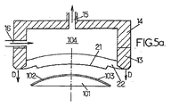
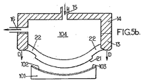
図5aおよび図5bは本発明の実施例を示しており、スタンプは、ダイアフラム20によって境界付けられた、密封された筐体104をさらに備える。筐体104は、剛体部13の上方にキャップ14を合致させることによって形成される。スタンプ表面21の形状は、開口部15を用いて、筐体104内の空気圧により制御できる。凸面の受け側表面103を有するレンズ101に対して、スタンプ表面21は前段階では凹面にされ、その絶対曲率半径は、受け側表面103の絶対曲率半径よりも大きい(図5a)。このことは、開口部15を用いて筐体104内の空気圧を低下させることによって得られる。このように、ダイアフラム20は最初に既に湾曲しており、スタンプが受け側表面103に対して押し下げられたときに生じるスタンプ表面21の残留歪みが減少する。スタンプ表面21の残留歪みが減少することで、受け側表面に印刷したパターンの品質が向上する。このことは、スタンプ表面21の歪みが空気圧制御によってさらに均一的に分布すること、および受け側表面103上のダイアフラム20の滑りが、スタンプ動作中に殆ど生じないことによる。必要に応じて、キャップ14はさらに小さいボア16を有し、そのボア16は、スタンプ動作中の圧力差を調節できる。
FIGS. 5 a and 5 b show an embodiment of the present invention where the stamp further comprises a sealed
受け側表面103が凹面である場合(図5b)、スタンプ表面21は最初に凸面とされ、受け側表面の絶対曲率半径よりも小さい絶対曲率半径を有する。これは、開口部15を用いて筐体104内の空気圧を高めることによって達成される。この圧力が筐体104の外部の圧力よりも高い場合、スタンプ表面は凸面となる。次いで、方向Dに沿ってスタンプを押し下げると、スタンプ表面21は、受け側表面103に深く入り込んで行き、その結果、最初の接触がスタンプ表面の中心点において生じる。必要に応じて、キャップ14は別の小さなボア16を有し、該ボア16はスタンプ動作中の圧力差を調節できる。
If the receiving
スタンプを対象物から取り除いた後、レンズ101の受け側表面103はエッチング剤と接触し、その結果、導電層102は、スタンプ動作中にインクが堆積していない受け側表面の点においてエッチングされる。ウェット・エッチングとして公知のプロセスは、導電層の材料に応じて、用いることができる。特に、40mモル/リットルの硝酸鉄(Fe(NO3)3)および60mモル/リットルのチオ尿素(CH4N2S)を含む溶液が、周囲温度において、金層をエッチングするのに適している。エッチング溶液としてpH調整されたシアン化物溶液を使用することもできる。エッチングの後、導電層102は、パターンPに従い、スタンプによって堆積されたインクでコーティングされている点のみに残る。
After removing the stamp from the object, the receiving
図6aおよび図6bは、レンズ101の受け側表面103に印刷されたパターンPの一例を示す。図6bは、図6aに示した矢印VIbに従った、レンズ101の断面図である。パターンPは線形の導電性グリッドであり、一組の平行な導電ライン110から構成される。各ラインは導電層102の残りの部分に対応する。有利には、グリッドは、0.1μmから0.4μmの範囲内、好ましくは0.14μmから0.25μmの範囲内の間隔pを有する。そして、レンズ101上に当たる可視光には回折が生じず、その結果、レンズは眼科用レンズの審美的要件に適合する。グリッドは光学用レンズに当たる光に、部分的な偏光作用を生じさせる。公知の方法において、その偏光作用は、反射平面により生じるグレアを低減するのに有用である。グリッドの他の特徴は、層102の材料に応じた、銀またはアルミニウムを材料とするグリッドラインと層102の厚さに応じた、30nm(ナノメートル)以上のラインの厚さtとスタンプ表面21上に複製されたパターンPによって指定される0.15μm以下のライン幅とグリッドラインに対し直交する偏光成分に対して16%から95%の範囲内とされ、かつグリッドラインと平行な偏光成分に対して0%から5%の範囲内とされるレンズの可視光域における透過率(visible transmission)であり得る。
6a and 6b show an example of a pattern P printed on the receiving
極性を有する線形のグリッド(polarizing linear grid)の幾何形状パラメータが、導電層102の特定の性質に適合することは明らかである。このパターンの例は、例示目的のためだけに挙げたものである。偏光以外の機能を用いて、他のパターンをレンズ上に印刷することもできる。本発明の製造方法を用いて、発明者らはまた、通常、波長1.3μmまたは1.5μmの赤外光を使用してレンズを製造した。
It is clear that the polarizing linear grid geometry parameters are adapted to the specific properties of the
さらに、詳細に記載された本発明は、ソフトリソグラフィの特定の用途および様々な実施形態に応じるために適合させ、または修正できることは明らかである。例えば、記載された実施から直接に導かれることが可能である方法において、パターンはポジティブまたはネガティブに印刷され得る。特に、「Positive Microcontact Printing」という技術を実施するために、本発明を用いることは容易である。この例は、非特許文献3に記載されている。本発明はまた、スタンプ上のインクとして特定の触媒分子を用いることによって、「Electroless deposition」の技術を実施するために有用である。この例は、非特許文献4に記載されている。本発明はまた、UVエンボス加工または熱エンボス加工などのマイクロモールド技術を実施するために有用であり得る。いくつかの例は、非特許文献1に記載されている。UVエンボス加工の特定の場合においては、スタンプのエラストマ系材料は、UV光を適度に透過させる必要がある。 Further, it will be apparent that the invention described in detail can be adapted or modified to suit a particular application and various embodiments of soft lithography. For example, the pattern can be printed positively or negatively in a way that can be derived directly from the described implementation. In particular, it is easy to use the present invention to implement a technique called “Positive Microcontact Printing”. This example is described in Non-Patent Document 3. The present invention is also useful for implementing the “Electroless deposition” technique by using specific catalyst molecules as ink on the stamp. This example is described in Non-Patent Document 4. The present invention may also be useful for implementing micromold techniques such as UV embossing or hot embossing. Some examples are described in Non-Patent Document 1. In the particular case of UV embossing, the elastomeric material of the stamp needs to be transparent to UV light.
また、別の実施形態において、本発明は、対象物(101)の擬似球面状をなした受け側表面(103)に印刷されたパターン(P)を有する対象物を製造する方法を提供し、受け側表面に重合性液体を塗布する工程と、UV光を透過するシロキサン型エラストマを含むスタンプを用いる工程と、対象物の受け側表面(103)に対してスタンプ表面(21)を押圧する工程であって、UV光で液体を硬化させる、工程と、対象物からスタンプを除去する工程とを含む。 In another embodiment, the present invention provides a method of manufacturing an object having a pattern (P) printed on a receiving surface (103) having a pseudo-spherical shape of the object (101), Applying a polymerizable liquid to the receiving surface, using a stamp containing a siloxane-type elastomer that transmits UV light, and pressing the stamp surface (21) against the receiving surface (103) of the object And curing the liquid with UV light and removing the stamp from the object.
同様の方法において、本発明の目的は、対象物(101)の擬似球面状をなした受け側表面(103)に印刷されたパターン(P)を有する対象物を製造する方法を提供し、スタンプ表面に重合性液体を塗布する工程と、UV光を透過するシロキサン型エラストマを含むスタンプを用いる工程と、対象物の受け側表面(103)に対してスタンプ表面(21)を押圧する工程であって、UV光で液体を硬化させる、工程と、対象物からスタンプを除去する工程とを含む。 In a similar manner, the object of the present invention is to provide a method for producing an object having a pattern (P) printed on a receiving surface (103) in the form of a pseudo-spherical surface of the object (101). A step of applying a polymerizable liquid to the surface, a step of using a stamp containing a siloxane-type elastomer that transmits UV light, and a step of pressing the stamp surface (21) against the receiving surface (103) of the object. And curing the liquid with UV light and removing the stamp from the object.
上記にて引用した両方の成形方法において、重合性液体を熱硬化することもまた実施可能であることは明らかである。 It is clear that in both molding methods cited above, it is also feasible to heat cure the polymerizable liquid.
Claims (37)
前記モールドサイド部分の内底端部が前記パターン(P)を囲むように、前記モールドサイド部分(2)を前記モールド底部(1)上に配置する工程であって、前記モールドサイド部分(2)は、下側モールドサイド部分(12)および上側モールドサイド部分(13)を備え、個々の内部ボアは一列に並んでおり、前記モールドサイド部分のうちの一つの前記ボアが他のモールドサイド部分のボアよりも断面においてより大きくされた、工程と、
前記下側モールドサイド部分(12)のボアの高さ(h)よりも高い厚さ(e)を有するエラストマダイアフラム(20)を形成するために重ね合わされた前記モールド底部(1)および前記モールドサイド部分(2)を備える前記モールド(100)に、少なくとも一つのエラストマ前駆物質を注入する工程と、
前記下側モールドサイド部分および前記上側モールドサイド部分のうちの最大のボアに対応する前記ダイアフラム(20)の周縁部に沿って、前記ダイアフラムを剛体部(13)に固定する工程と
を含む、スタンプ製造方法。 Providing the mold bottom (1) with a pattern (P) replicated on a plane of the mold bottom;
Disposing the mold side portion (2) on the mold bottom portion (1) such that an inner bottom end of the mold side portion surrounds the pattern (P), the mold side portion (2) Comprises a lower mold side part (12) and an upper mold side part (13), the individual internal bores are arranged in a line, and one of the mold side parts is connected to the other mold side part. A process made larger in cross-section than bore,
The mold bottom (1) and the mold side overlaid to form an elastomer diaphragm (20) having a thickness (e) that is higher than the height (h) of the bore in the lower mold side portion (12). Injecting at least one elastomer precursor into said mold (100) comprising part (2);
Fixing the diaphragm to a rigid body portion (13) along a peripheral edge portion of the diaphragm (20) corresponding to the largest bore of the lower mold side portion and the upper mold side portion. Production method.
請求項1から6、または8、または9のいずれか一項に記載のスタンプの前記スタンプ表面(21)にインクを塗布する工程と、
前記対象物の受け側表面(103)に対して、前記スタンプのスタンプ表面(21)を押圧する工程と、
前記対象物から前記スタンプを取り除く工程と、
ウェット・エッチングまたは化学メッキ法によって前記受け側表面を加工する工程と
を含む、方法。 A method of manufacturing the object having a pattern (P) printed on a receiving surface (103) having a pseudo-spherical shape of the object (101),
Applying ink to the stamp surface (21) of the stamp according to any one of claims 1 to 6, or 8, or 9;
Pressing the stamp surface (21) of the stamp against the receiving surface (103) of the object;
Removing the stamp from the object;
Processing the receiving surface by wet etching or chemical plating.
凹面のスタンプ表面に光吸収層を積層する工程と、
前記受け側表面にフォトレジストを適用する工程と、
前記対象物の受け側表面(103)に前記スタンプ表面(21)を押圧することによって、光結合マスクとして、請求項1から5または請求項7から9のいずれか一項に記載の前記スタンプを用いる工程であって、前記スタンプを紫外光に曝す、工程と、
前記対象物から前記スタンプを取り除く工程と、
フォトレジストを現像する工程と
を含む、方法。 A method of manufacturing the object having a pattern (P) printed on a receiving surface (103) having a pseudo-spherical shape of the object (101),
A step of laminating a light absorbing layer on the concave stamp surface;
Applying a photoresist to the receiving surface;
The stamp according to any one of claims 1 to 5 or 7 to 9 as a light coupling mask by pressing the stamp surface (21) against the receiving surface (103) of the object. A step of exposing the stamp to ultraviolet light; and
Removing the stamp from the object;
Developing the photoresist.
前記スタンプ表面(21)および前記受け側表面(103)が相補的形状を有し、かつ前記受け側表面に対して前記スタンプ表面を押圧することが前記スタンプ表面の中間部において接触することによって開始されるように、前記筐体(104)内の圧力を調整する工程
をさらに含む、請求項5または請求項16から18のいずれか一項に記載の対象物を製造する方法。 Before pressing the stamp surface (21) of the stamp against the receiving surface (103) of the object,
The stamp surface (21) and the receiver surface (103) have complementary shapes, and pressing the stamp surface against the receiver surface starts by contacting at an intermediate portion of the stamp surface The method of manufacturing an object according to any one of claims 5 or 16 to 18, further comprising adjusting the pressure in the housing (104) as described.
前記受け側表面に重合性液体を塗布する工程と、
請求項7に記載のスタンプを用いる工程と、
前記対象物の受け側表面(103)にスタンプ表面(21)を押圧する工程であって、紫外光で液体を硬化させる、工程と、
対象物からスタンプを除去する工程と
を含む、方法。 A method of manufacturing the object having a pattern (P) printed on a receiving surface (103) having a pseudo-spherical shape of the object (101),
Applying a polymerizable liquid to the receiving surface;
Using the stamp of claim 7;
Pressing the stamp surface (21) against the receiving surface (103) of the object, curing the liquid with ultraviolet light; and
Removing the stamp from the object.
前記スタンプ表面に重合性液体を塗布する工程と、
請求項7に記載のスタンプを用いる工程と、前記対象物の受け側表面(103)にスタンプ表面(21)を押圧する工程であって、紫外光で液体を硬化させる、工程と、
対象物からスタンプを除去する工程と
を含む、方法。 A method of manufacturing the object having a pattern (P) printed on a receiving surface (103) having a pseudo-spherical shape of the object (101),
Applying a polymerizable liquid to the stamp surface;
Using the stamp of claim 7, and pressing the stamp surface (21) against the receiving surface (103) of the object, curing the liquid with ultraviolet light; and
Removing the stamp from the object.
前記受け側表面に重合性液体を塗布する工程と、
請求項1から6のいずれか一項に記載のスタンプを用いる工程と、
前記対象物の受け側表面(103)にスタンプ表面(21)を押圧する工程であって、熱硬化で液体を硬化させる、工程と、
対象物からスタンプを除去する工程と
を含む、方法。 A method of manufacturing the object having a pattern (P) printed on a receiving surface (103) having a pseudo-spherical shape of the object (101),
Applying a polymerizable liquid to the receiving surface;
Using the stamp according to any one of claims 1 to 6;
Pressing the stamp surface (21) against the receiving surface (103) of the object, curing the liquid by thermosetting;
Removing the stamp from the object.
前記スタンプ表面に重合性液体を塗布する工程と、
請求項1から6のいずれか一項に記載のスタンプを用いる工程と、
前記対象物の受け側表面(103)にスタンプ表面(21)を押圧する工程であって、熱硬化で液体を硬化させる、工程と、
対象物からスタンプを除去する工程と
を含む、方法。 A method of manufacturing the object having a pattern (P) printed on a receiving surface (103) having a pseudo-spherical shape of the object (101),
Applying a polymerizable liquid to the stamp surface;
Using the stamp according to any one of claims 1 to 6;
Pressing the stamp surface (21) against the receiving surface (103) of the object, curing the liquid by thermosetting;
Removing the stamp from the object.
Applications Claiming Priority (2)
| Application Number | Priority Date | Filing Date | Title |
|---|---|---|---|
| EP04292954A EP1669196B1 (en) | 2004-12-10 | 2004-12-10 | Stamp for patterning, method for manufacturing such stamp and method for manufacturing an object using the stamp. |
| PCT/EP2005/013529 WO2006061255A1 (en) | 2004-12-10 | 2005-12-01 | Stamp for patterning, method for manufacturing such stamp and method for manufacturing an object using the stamp |
Publications (1)
| Publication Number | Publication Date |
|---|---|
| JP2008522867A true JP2008522867A (en) | 2008-07-03 |
Family
ID=34931592
Family Applications (1)
| Application Number | Title | Priority Date | Filing Date |
|---|---|---|---|
| JP2007544845A Pending JP2008522867A (en) | 2004-12-10 | 2005-12-01 | Patterning stamp, method for manufacturing the stamp, and method for manufacturing an object using the stamp |
Country Status (6)
| Country | Link |
|---|---|
| US (1) | US8268544B2 (en) |
| EP (2) | EP1669196B1 (en) |
| JP (1) | JP2008522867A (en) |
| AT (1) | ATE396048T1 (en) |
| DE (1) | DE602004014002D1 (en) |
| WO (1) | WO2006061255A1 (en) |
Cited By (2)
| Publication number | Priority date | Publication date | Assignee | Title |
|---|---|---|---|---|
| JP2020088286A (en) * | 2018-11-29 | 2020-06-04 | キヤノン株式会社 | Molding apparatus, molding method, and article manufacturing method |
| KR102415094B1 (en) * | 2021-11-17 | 2022-06-30 | 한국기계연구원 | Exposure apparatus and method for nanoimprint process for non-planar substrates |
Families Citing this family (22)
| Publication number | Priority date | Publication date | Assignee | Title |
|---|---|---|---|---|
| US20080160129A1 (en) * | 2006-05-11 | 2008-07-03 | Molecular Imprints, Inc. | Template Having a Varying Thickness to Facilitate Expelling a Gas Positioned Between a Substrate and the Template |
| JP5062551B2 (en) * | 2007-01-30 | 2012-10-31 | 株式会社吉野工業所 | Tampo printing method and tampo transfer material for tampo printing |
| US7678423B2 (en) * | 2007-02-27 | 2010-03-16 | The Regents Of The University Of Michigan | System and method for depositing thin layers on non-planar substrates by stamping |
| US20090020910A1 (en) * | 2007-02-27 | 2009-01-22 | Stephen Forrest | System and method for depositing thin layers on non-planar substrates by stamping |
| ATE484773T1 (en) | 2007-03-21 | 2010-10-15 | Erich Thallner | METHOD AND DEVICE FOR PRODUCING A NANOSTRUCTURED DISK |
| DE102007019398A1 (en) * | 2007-04-23 | 2008-11-06 | Itw Morlock Gmbh | Pad printing machine and tampon for it |
| DE102008001800A1 (en) | 2007-05-25 | 2008-11-27 | Carl Zeiss Smt Ag | Projection lens for microlithography, microlithography projection exposure apparatus with such a projection lens, microlithographic manufacturing method for components as well as produced by this method component |
| DE112008001634A5 (en) * | 2007-06-21 | 2010-04-01 | GeSIM Gesellschaft für Silizium-Mikrosysteme mbH | Method and device for transfer of micro- or nanostructures by contact stamping |
| US20090025595A1 (en) * | 2007-07-25 | 2009-01-29 | Nano Terra Inc. | Contact Printing Method Using an Elastomeric Stamp Having a Variable Surface Area and Variable Shape |
| WO2009129443A2 (en) * | 2008-04-17 | 2009-10-22 | Massachusetts Institute Of Technology | Diaphragm flexure with large range and high load capacity |
| US9793481B2 (en) * | 2008-10-01 | 2017-10-17 | The Regents Of The University Of Michigan | Patterning by stamped metal resist |
| KR20120034940A (en) * | 2010-10-04 | 2012-04-13 | 삼성전자주식회사 | Patterning mold and manufacturing method thereof |
| CN103429417A (en) * | 2011-05-19 | 2013-12-04 | 综研化学株式会社 | Nanoimprint mold and curved body |
| TW201321214A (en) * | 2011-11-29 | 2013-06-01 | Wistron Corp | Embossing method and embossing mold |
| JP2014226859A (en) * | 2013-05-23 | 2014-12-08 | 株式会社秀峰 | Printing method |
| US20150108673A1 (en) * | 2013-10-18 | 2015-04-23 | The Chinese University Of Hong Kong | Imprinting apparatus and method for imprinting |
| US10675975B2 (en) * | 2015-04-17 | 2020-06-09 | Visteon Global Technologies, Inc. | Glass lens assembly with an elastic adhesive |
| US11840013B2 (en) * | 2018-02-27 | 2023-12-12 | Matthews International Corporation | Graphite materials and devices with surface micro-texturing |
| JP7348182B2 (en) * | 2018-07-23 | 2023-09-20 | 株式会社日立ハイテク | Concave diffraction grating manufacturing method, manufacturing device, and concave diffraction grating |
| CN109656098A (en) * | 2018-12-04 | 2019-04-19 | 上海安翰医疗技术有限公司 | Production method, nano impression Elastic forming board and the component of nano impression Elastic forming board |
| DE102021130516A1 (en) * | 2021-11-22 | 2023-05-25 | Tampoprint Gmbh | Method and device for printing or decorating an object |
| US11717728B1 (en) * | 2022-02-28 | 2023-08-08 | Acushnet Company | Golf ball having markings spaced from a centerline plane |
Citations (6)
| Publication number | Priority date | Publication date | Assignee | Title |
|---|---|---|---|---|
| JPH01232048A (en) * | 1988-03-12 | 1989-09-18 | Nec Corp | Contact printer |
| JPH09240125A (en) * | 1996-03-04 | 1997-09-16 | Motorola Inc | Apparatus for stamping surface of article and method therefor |
| DE10028620A1 (en) * | 2000-06-09 | 2001-12-20 | Heinrich Bielmeier | Ink dabber with housing and elastic membrane fastened to it to print onto uneven surfaces by projection of two-dimensional pictures onto three-dimensional surfaces |
| JP2002040202A (en) * | 2000-07-21 | 2002-02-06 | Seiko Epson Corp | Method and device for coloring plastic lens |
| JP2003086537A (en) * | 2001-09-13 | 2003-03-20 | Tdk Corp | Thin film pattern manufacturing method using structure and the structure |
| WO2003099463A2 (en) * | 2002-05-27 | 2003-12-04 | Koninklijke Philips Electronics N.V. | Method and device for transferring a pattern from a stamp to a substrate |
Family Cites Families (22)
| Publication number | Priority date | Publication date | Assignee | Title |
|---|---|---|---|---|
| US2748696A (en) * | 1951-06-13 | 1956-06-05 | Murray Lilian | Printing or decoration of ceramic or other ware |
| US4508031A (en) * | 1981-12-21 | 1985-04-02 | Corning Glass Works | Flexible membrane printing apparatus for a decorating machine |
| US6180239B1 (en) | 1993-10-04 | 2001-01-30 | President And Fellows Of Harvard College | Microcontact printing on surfaces and derivative articles |
| EP0812434B1 (en) | 1995-03-01 | 2013-09-18 | President and Fellows of Harvard College | Microcontact printing on surfaces and derivative articles |
| US5804017A (en) * | 1995-07-27 | 1998-09-08 | Imation Corp. | Method and apparatus for making an optical information record |
| EP0784542B1 (en) | 1995-08-04 | 2001-11-28 | International Business Machines Corporation | Stamp for a lithographic process |
| EP0784543B1 (en) | 1995-08-04 | 2000-04-26 | International Business Machines Corporation | Lithographic surface or thin layer modification |
| US6060121A (en) | 1996-03-15 | 2000-05-09 | President And Fellows Of Harvard College | Microcontact printing of catalytic colloids |
| EP0865323B1 (en) | 1996-09-06 | 2002-11-20 | International Business Machines Corporation | Method of oriented depositing chemically defined bodies |
| US5948621A (en) * | 1997-09-30 | 1999-09-07 | The United States Of America As Represented By The Secretary Of The Navy | Direct molecular patterning using a micro-stamp gel |
| US5937758A (en) | 1997-11-26 | 1999-08-17 | Motorola, Inc. | Micro-contact printing stamp |
| US6871951B2 (en) * | 2000-06-23 | 2005-03-29 | E-Vision, Llc | Electro-optic lens with integrated components |
| US6517995B1 (en) * | 1999-09-14 | 2003-02-11 | Massachusetts Institute Of Technology | Fabrication of finely featured devices by liquid embossing |
| TW562755B (en) | 1999-12-31 | 2003-11-21 | Ibm | Stamp device for printing a pattern on a surface of a substrate |
| US6542307B2 (en) * | 2000-10-20 | 2003-04-01 | Three-Five Systems, Inc. | Compact near-eye illumination system |
| US7338613B2 (en) | 2001-09-10 | 2008-03-04 | Surface Logix, Inc. | System and process for automated microcontact printing |
| AU2003217184A1 (en) * | 2002-01-11 | 2003-09-02 | Massachusetts Institute Of Technology | Microcontact printing |
| US6656308B2 (en) * | 2002-04-22 | 2003-12-02 | International Business Machines Corporation | Process of fabricating a precision microcontact printing stamp |
| US6792856B2 (en) | 2002-07-16 | 2004-09-21 | International Business Machines Corporation | Method and apparatus for accurate, micro-contact printing |
| US20040046927A1 (en) * | 2002-08-27 | 2004-03-11 | Montgomery Mark E. | Polarized and non-polarized bifocal spectacles |
| US6981445B2 (en) * | 2003-12-24 | 2006-01-03 | Axela Biosensors Inc. | Method and apparatus for micro-contact printing |
| DE102005028704B4 (en) * | 2005-06-20 | 2016-09-08 | Infineon Technologies Ag | A method of manufacturing a semiconductor device having semiconductor device components embedded in plastic package |
-
2004
- 2004-12-10 AT AT04292954T patent/ATE396048T1/en not_active IP Right Cessation
- 2004-12-10 EP EP04292954A patent/EP1669196B1/en active Active
- 2004-12-10 DE DE602004014002T patent/DE602004014002D1/en active Active
-
2005
- 2005-12-01 WO PCT/EP2005/013529 patent/WO2006061255A1/en active Application Filing
- 2005-12-01 US US11/721,199 patent/US8268544B2/en active Active
- 2005-12-01 EP EP05824198A patent/EP1819514A1/en not_active Withdrawn
- 2005-12-01 JP JP2007544845A patent/JP2008522867A/en active Pending
Patent Citations (6)
| Publication number | Priority date | Publication date | Assignee | Title |
|---|---|---|---|---|
| JPH01232048A (en) * | 1988-03-12 | 1989-09-18 | Nec Corp | Contact printer |
| JPH09240125A (en) * | 1996-03-04 | 1997-09-16 | Motorola Inc | Apparatus for stamping surface of article and method therefor |
| DE10028620A1 (en) * | 2000-06-09 | 2001-12-20 | Heinrich Bielmeier | Ink dabber with housing and elastic membrane fastened to it to print onto uneven surfaces by projection of two-dimensional pictures onto three-dimensional surfaces |
| JP2002040202A (en) * | 2000-07-21 | 2002-02-06 | Seiko Epson Corp | Method and device for coloring plastic lens |
| JP2003086537A (en) * | 2001-09-13 | 2003-03-20 | Tdk Corp | Thin film pattern manufacturing method using structure and the structure |
| WO2003099463A2 (en) * | 2002-05-27 | 2003-12-04 | Koninklijke Philips Electronics N.V. | Method and device for transferring a pattern from a stamp to a substrate |
Cited By (3)
| Publication number | Priority date | Publication date | Assignee | Title |
|---|---|---|---|---|
| JP2020088286A (en) * | 2018-11-29 | 2020-06-04 | キヤノン株式会社 | Molding apparatus, molding method, and article manufacturing method |
| JP7171394B2 (en) | 2018-11-29 | 2022-11-15 | キヤノン株式会社 | Molding Apparatus, Molding Method, and Article Manufacturing Method |
| KR102415094B1 (en) * | 2021-11-17 | 2022-06-30 | 한국기계연구원 | Exposure apparatus and method for nanoimprint process for non-planar substrates |
Also Published As
| Publication number | Publication date |
|---|---|
| US8268544B2 (en) | 2012-09-18 |
| ATE396048T1 (en) | 2008-06-15 |
| EP1819514A1 (en) | 2007-08-22 |
| WO2006061255A1 (en) | 2006-06-15 |
| EP1669196A1 (en) | 2006-06-14 |
| EP1669196B1 (en) | 2008-05-21 |
| US20090208882A1 (en) | 2009-08-20 |
| DE602004014002D1 (en) | 2008-07-03 |
Similar Documents
| Publication | Publication Date | Title |
|---|---|---|
| JP2008522867A (en) | Patterning stamp, method for manufacturing the stamp, and method for manufacturing an object using the stamp | |
| JP5225618B2 (en) | Nanoimprint mold and manufacturing method thereof | |
| JP6173354B2 (en) | Light transmission type imprint mold, large area mold manufacturing method | |
| US7632087B2 (en) | Composite stamper for imprint lithography | |
| JP5411557B2 (en) | Microstructure transfer device | |
| WO2016006592A1 (en) | Mold for step-and-repeat imprinting, and method for producing same | |
| JP5633744B2 (en) | Substrate preparation method, nanoimprint lithography method and mold replication method | |
| JP4448868B2 (en) | Imprint stamper and manufacturing method thereof | |
| TWI576229B (en) | Safe separation for nano imprinting | |
| JP5761320B2 (en) | Manufacturing method of stamp for micro contact printing | |
| KR20100008619A (en) | Fabrication mehtod of lithography mask and formation method of fine pattern using the same | |
| KR100889814B1 (en) | A stamper and Production method thereof and Imprinting process of substrate using the stamper | |
| US9180608B2 (en) | Stamp, method of manufacturing the same, and imprinting method using the stamp | |
| KR101542942B1 (en) | Method of forming a metal nano-pattern for controlling plasmonic characteristics | |
| KR20110140059A (en) | Stamp for nano-imprint and manufacturing method thereof | |
| JP5428449B2 (en) | Method for producing master plate for producing stamp for micro contact printing, and master plate for producing stamp for micro contact printing | |
| KR102415094B1 (en) | Exposure apparatus and method for nanoimprint process for non-planar substrates | |
| KR101977122B1 (en) | Nano mold and method of fabricating thereof | |
| KR101993385B1 (en) | method for manufacturing stamp | |
| JPWO2020080372A1 (en) | Fine pattern molding method, imprint mold manufacturing method and imprint mold and optical device | |
| KR20090102994A (en) | Roller for imprinting |
Legal Events
| Date | Code | Title | Description |
|---|---|---|---|
| A621 | Written request for application examination |
Free format text: JAPANESE INTERMEDIATE CODE: A621 Effective date: 20080815 |
|
| A131 | Notification of reasons for refusal |
Free format text: JAPANESE INTERMEDIATE CODE: A131 Effective date: 20110426 |
|
| A601 | Written request for extension of time |
Free format text: JAPANESE INTERMEDIATE CODE: A601 Effective date: 20110705 |
|
| A602 | Written permission of extension of time |
Free format text: JAPANESE INTERMEDIATE CODE: A602 Effective date: 20110712 |
|
| A02 | Decision of refusal |
Free format text: JAPANESE INTERMEDIATE CODE: A02 Effective date: 20111108 |