JP2008270762A - Method of manufacturing semiconductor device - Google Patents
Method of manufacturing semiconductor device Download PDFInfo
- Publication number
- JP2008270762A JP2008270762A JP2008062132A JP2008062132A JP2008270762A JP 2008270762 A JP2008270762 A JP 2008270762A JP 2008062132 A JP2008062132 A JP 2008062132A JP 2008062132 A JP2008062132 A JP 2008062132A JP 2008270762 A JP2008270762 A JP 2008270762A
- Authority
- JP
- Japan
- Prior art keywords
- substrate
- element substrate
- organic resin
- fibrous body
- forming
- Prior art date
- Legal status (The legal status is an assumption and is not a legal conclusion. Google has not performed a legal analysis and makes no representation as to the accuracy of the status listed.)
- Withdrawn
Links
Images


Classifications
-
- H—ELECTRICITY
- H01—ELECTRIC ELEMENTS
- H01L—SEMICONDUCTOR DEVICES NOT COVERED BY CLASS H10
- H01L23/00—Details of semiconductor or other solid state devices
- H01L23/28—Encapsulations, e.g. encapsulating layers, coatings, e.g. for protection
- H01L23/29—Encapsulations, e.g. encapsulating layers, coatings, e.g. for protection characterised by the material, e.g. carbon
- H01L23/293—Organic, e.g. plastic
-
- H—ELECTRICITY
- H01—ELECTRIC ELEMENTS
- H01L—SEMICONDUCTOR DEVICES NOT COVERED BY CLASS H10
- H01L21/00—Processes or apparatus adapted for the manufacture or treatment of semiconductor or solid state devices or of parts thereof
- H01L21/02—Manufacture or treatment of semiconductor devices or of parts thereof
- H01L21/04—Manufacture or treatment of semiconductor devices or of parts thereof the devices having at least one potential-jump barrier or surface barrier, e.g. PN junction, depletion layer or carrier concentration layer
- H01L21/18—Manufacture or treatment of semiconductor devices or of parts thereof the devices having at least one potential-jump barrier or surface barrier, e.g. PN junction, depletion layer or carrier concentration layer the devices having semiconductor bodies comprising elements of Group IV of the Periodic System or AIIIBV compounds with or without impurities, e.g. doping materials
- H01L21/20—Deposition of semiconductor materials on a substrate, e.g. epitaxial growth solid phase epitaxy
-
- H—ELECTRICITY
- H01—ELECTRIC ELEMENTS
- H01L—SEMICONDUCTOR DEVICES NOT COVERED BY CLASS H10
- H01L27/00—Devices consisting of a plurality of semiconductor or other solid-state components formed in or on a common substrate
- H01L27/02—Devices consisting of a plurality of semiconductor or other solid-state components formed in or on a common substrate including semiconductor components specially adapted for rectifying, oscillating, amplifying or switching and having at least one potential-jump barrier or surface barrier; including integrated passive circuit elements with at least one potential-jump barrier or surface barrier
- H01L27/12—Devices consisting of a plurality of semiconductor or other solid-state components formed in or on a common substrate including semiconductor components specially adapted for rectifying, oscillating, amplifying or switching and having at least one potential-jump barrier or surface barrier; including integrated passive circuit elements with at least one potential-jump barrier or surface barrier the substrate being other than a semiconductor body, e.g. an insulating body
- H01L27/1214—Devices consisting of a plurality of semiconductor or other solid-state components formed in or on a common substrate including semiconductor components specially adapted for rectifying, oscillating, amplifying or switching and having at least one potential-jump barrier or surface barrier; including integrated passive circuit elements with at least one potential-jump barrier or surface barrier the substrate being other than a semiconductor body, e.g. an insulating body comprising a plurality of TFTs formed on a non-semiconducting substrate, e.g. driving circuits for AMLCDs
-
- H—ELECTRICITY
- H01—ELECTRIC ELEMENTS
- H01L—SEMICONDUCTOR DEVICES NOT COVERED BY CLASS H10
- H01L2924/00—Indexing scheme for arrangements or methods for connecting or disconnecting semiconductor or solid-state bodies as covered by H01L24/00
- H01L2924/0001—Technical content checked by a classifier
- H01L2924/0002—Not covered by any one of groups H01L24/00, H01L24/00 and H01L2224/00
-
- H—ELECTRICITY
- H01—ELECTRIC ELEMENTS
- H01L—SEMICONDUCTOR DEVICES NOT COVERED BY CLASS H10
- H01L2924/00—Indexing scheme for arrangements or methods for connecting or disconnecting semiconductor or solid-state bodies as covered by H01L24/00
- H01L2924/10—Details of semiconductor or other solid state devices to be connected
- H01L2924/11—Device type
- H01L2924/12—Passive devices, e.g. 2 terminal devices
- H01L2924/1204—Optical Diode
- H01L2924/12044—OLED
-
- H—ELECTRICITY
- H05—ELECTRIC TECHNIQUES NOT OTHERWISE PROVIDED FOR
- H05K—PRINTED CIRCUITS; CASINGS OR CONSTRUCTIONAL DETAILS OF ELECTRIC APPARATUS; MANUFACTURE OF ASSEMBLAGES OF ELECTRICAL COMPONENTS
- H05K1/00—Printed circuits
- H05K1/18—Printed circuits structurally associated with non-printed electric components
- H05K1/182—Printed circuits structurally associated with non-printed electric components associated with components mounted in the printed circuit board, e.g. insert mounted components [IMC]
- H05K1/185—Components encapsulated in the insulating substrate of the printed circuit or incorporated in internal layers of a multilayer circuit
-
- H—ELECTRICITY
- H05—ELECTRIC TECHNIQUES NOT OTHERWISE PROVIDED FOR
- H05K—PRINTED CIRCUITS; CASINGS OR CONSTRUCTIONAL DETAILS OF ELECTRIC APPARATUS; MANUFACTURE OF ASSEMBLAGES OF ELECTRICAL COMPONENTS
- H05K1/00—Printed circuits
- H05K1/18—Printed circuits structurally associated with non-printed electric components
- H05K1/189—Printed circuits structurally associated with non-printed electric components characterised by the use of a flexible or folded printed circuit
Abstract
Description
本発明は、単結晶半導体基板またはSOI基板を用いて形成された半導体素子を有する半導体装置の作製方法に関する。 The present invention relates to a method for manufacturing a semiconductor device having a semiconductor element formed using a single crystal semiconductor substrate or an SOI substrate.
現在、無線チップ、センサ等、各種装置の薄型化が製品小型化の上で重要な要素となっており、薄型化技術や小型化製品の使用範囲が急速に広まっている。これらの薄型化された各種装置はある程度フレキシブルなため、湾曲したものに設置して使用することが可能である。 At present, thinning of various devices such as a wireless chip and a sensor is an important element in downsizing the product, and the range of use of thinning technology and downsized products is rapidly widening. Since these various thinned devices are flexible to some extent, they can be installed and used on curved surfaces.
また、特許文献1では、0.5mm以下サイズの半導体チップを紙またはフィルム状の媒体に埋め込み、曲げや集中荷重を改善した半導体装置が開示されている。
しかしながら、アンテナをチップに作り込んで内蔵(オンチップ化)する半導体装置の場合、チップの面積が小さいとアンテナサイズが小さくなり通信距離が短くなる問題がある。また、紙またはフィルム媒体に設けられたアンテナをチップに接続して半導体装置を作製する場合、チップの大きさが小さいと、接続不良が生じ、歩留まりが低下する。 However, in the case of a semiconductor device in which an antenna is built in a chip (on-chip), there is a problem that if the chip area is small, the antenna size is reduced and the communication distance is shortened. In addition, in the case where a semiconductor device is manufactured by connecting an antenna provided on paper or a film medium to a chip, if the size of the chip is small, a connection failure occurs and the yield decreases.
そこで本発明は、外部からの局所的押圧による非破壊の信頼性が高い半導体装置を歩留まり高く作製する方法を提供する。 Therefore, the present invention provides a method for manufacturing a semiconductor device with high non-destructive reliability by local pressing from outside with high yield.
本発明は、単結晶基板またはSOI基板を用いて形成された半導体素子を有する素子基板を形成し、素子基板上に有機化合物または無機化合物の繊維体を設け、素子基板及び繊維体上から有機樹脂を含む組成物を塗布し、加熱することにより、素子基板上に有機化合物または無機化合物の繊維体に有機樹脂が含浸された封止層を形成して半導体装置を作製することを特徴とする。 The present invention forms an element substrate having a semiconductor element formed using a single crystal substrate or an SOI substrate, and provides a fiber body of an organic compound or an inorganic compound on the element substrate, and an organic resin is formed on the element substrate and the fiber body. A semiconductor device is manufactured by forming a sealing layer in which a fibrous body of an organic compound or an inorganic compound is impregnated with an organic resin over an element substrate by applying and heating a composition containing the above.
また、本発明は、単結晶基板またはSOI基板を用いて形成された半導体素子を有する素子基板を形成し、素子基板上から有機樹脂を含む組成物を塗布し、素子基板及び有機樹脂層上に有機化合物または無機化合物の繊維体を設け、加熱することにより、素子基板上に有機化合物または無機化合物の繊維体に有機樹脂が含浸された封止層を形成して半導体装置を作製することを特徴とする。 The present invention also includes forming an element substrate having a semiconductor element formed using a single crystal substrate or an SOI substrate, applying a composition containing an organic resin from the element substrate, and forming the element substrate and the organic resin layer on the element substrate and the organic resin layer. A semiconductor device is manufactured by forming a sealing body in which an organic compound or an inorganic compound fiber body is impregnated with an organic resin on an element substrate by providing an organic compound or inorganic compound fiber body and heating. And
素子基板の厚さは1μm以上80μm以下、さらには1μm以上50μm以下、さらには1μm以上20μm以下、1μm以上10μm以下、さらには1μm以上5μm以下であり、封止層の厚さは厚さ10μm以上100μm以下であることが好ましい。このような厚さにすることにより、湾曲することが可能な半導体装置を作製することができる。 The thickness of the element substrate is 1 μm or more and 80 μm or less, further 1 μm or more and 50 μm or less, 1 μm or more and 20 μm or less, 1 μm or more and 10 μm or less, further 1 μm or more and 5 μm or less, and the sealing layer thickness is 10 μm or more. It is preferable that it is 100 micrometers or less. With such a thickness, a semiconductor device that can be bent can be manufactured.
繊維体としては、有機化合物または無機化合物の高強度繊維を用いた織布または不織布がある。高強度繊維としては、具体的には引張弾性率が高い繊維である。またはヤング率が高い繊維である。 Examples of the fiber body include a woven fabric and a nonwoven fabric using high-strength fibers of an organic compound or an inorganic compound. Specifically, the high-strength fiber is a fiber having a high tensile elastic modulus. Or it is a fiber with a high Young's modulus.
また、有機樹脂としては、熱可塑性樹脂または熱硬化性樹脂を用いることができる。 As the organic resin, a thermoplastic resin or a thermosetting resin can be used.
繊維体として高強度繊維を用いることにより、局所的な押圧が半導体装置にかかったとしても、当該圧力が繊維体全体に分散され、半導体装置の一部が延伸することを防ぐことができる。即ち、一部の延伸に伴う配線、半導体素子等の破壊を防止することが可能である。 By using high-strength fibers as the fibrous body, even if local pressing is applied to the semiconductor device, the pressure is dispersed throughout the fibrous body, and part of the semiconductor device can be prevented from stretching. That is, it is possible to prevent damage to wiring, semiconductor elements, and the like due to partial stretching.
本発明により、外部から局所的な圧力がかかっても破損しにくく、信頼性が高い半導体装置を歩留まり高く作製することができる。 According to the present invention, a highly reliable semiconductor device which is not easily damaged even when a local pressure is applied from the outside can be manufactured with high yield.
以下に、本発明の実施の形態を図面に基づいて説明する。但し、本発明は多くの異なる形態で実施することが可能であり、本発明の趣旨及びその範囲から逸脱することなくその形態及び詳細を様々に変更し得ることは当業者であれば容易に理解される。従って、本実施の形態の記載内容に限定して解釈されるものではない。なお、実施の形態を説明するための全図において、同一部分又は同様な機能を有する部分には同一の符号を付し、その繰り返しの説明は省略する。 Embodiments of the present invention will be described below with reference to the drawings. However, the present invention can be implemented in many different forms, and those skilled in the art can easily understand that the forms and details can be variously changed without departing from the spirit and scope of the present invention. Is done. Therefore, the present invention is not construed as being limited to the description of this embodiment mode. Note that in all the drawings for describing the embodiments, the same portions or portions having similar functions are denoted by the same reference numerals, and repetitive description thereof is omitted.
(実施の形態1)
本実施の形態では、外部からの局所的圧力がかかっても破損しにくい半導体装置を歩留まり高く作製する方法を、図1を用いて示す。
(Embodiment 1)
In this embodiment mode, a method for manufacturing a semiconductor device which is difficult to be damaged even when a local external pressure is applied with high yield will be described with reference to FIGS.
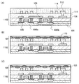
図1(A)に示すように、単結晶半導体基板またはSOI基板を用いて形成された半導体素子を含む素子基板1102及びアンテナ112を形成する。次に、素子基板1102及びアンテナ112上に、繊維体113を設ける。
As shown in FIG. 1A, an
素子基板1102に含まれる半導体素子の代表例としては、MOSトランジスタ、ダイオード、不揮発性記憶素子等の能動素子、抵抗素子、容量素子等の受動素子がある。また、単結晶半導体基板、代表的には、n型又はp型の導電型を有する単結晶シリコン基板(シリコンウェハ)、化合物半導体基板(GaAs基板、InP基板、GaN基板、SiC基板、サファイア基板、ZnSe基板等)を用いることが好ましい。また、SOI(Si−On−Insulator)基板を用いることもできる。SOI基板として、鏡面研磨ウェハに酸素イオンを注入した後、高温アニールすることにより、表面から一定の深さに酸化層を形成させるとともに、表面層に生じた欠陥を消滅させて作られた所謂SIMOX(Separation by IMplanted OXygen)基板や、水素イオン注入により形成された微小ボイドの熱処理による成長を利用してSi基板を劈開するスマートカット法や、ELTRAN法(Epitaxial Layer Transfer:キャノン社の登録商標)等を用いて形成したSOI基板を用いてもよい。素子基板1102の厚さとしては、1μm以上80μm以下、さらには1μm以上50μm以下、さらには1μm以上20μm以下、1μm以上10μm以下、さらには1μm以上5μm以下が好ましい。このような厚さにすることにより、湾曲することが可能な半導体装置を作製することができる。また、半導体装置の上面の面積は、4mm2以上、さらには9mm2以上が好ましい。
Typical examples of semiconductor elements included in the
素子基板1102に少なくともMOSトランジスタ、抵抗素子、容量素子、配線等が形成される場合、半導体装置として他の装置の制御やデータの計算・加工を行なうマイクロプロセッサ(MPU)を作製することができる。MPUは、CPU、メインメモリ、コントローラ、インターフェース、I/Oポート等を有する。
In the case where at least a MOS transistor, a resistor, a capacitor, a wiring, or the like is formed over the
また、素子基板1102に少なくとも、記憶素子及びMOSトランジスタが形成される場合、半導体装置として記憶装置を作製することができる。記憶素子としては、フローティングゲートまたは電荷蓄積層を有する不揮発性記憶素子、MOSトランジスタ及びそれに接続される容量素子、MOSトランジスタ及びそれに接続される強誘電体層を有する容量素子、一対の電極の間に有機化合物層が挟まれる有機メモリ素子等がある。また、このような記憶素子を有する半導体装置としては、DRAM(Dynamic Random Access Memory)、SRAM(Static Random Access Memory)、FeRAM(Ferroelectric Random Access Memory)、マスクROM(Read Only Memory)、EPROM(Electrically Programmable Read Only Memory)、EEPROM(Electrically Erasable and Programmable Read Only Memory)、フラッシュメモリ等の記憶装置がある。
In the case where at least a memory element and a MOS transistor are formed over the
また、素子基板1102に少なくとも、ダイオードが形成される場合、半導体装置として光センサ、イメージセンサ、太陽電池等を作製することができる。ダイオードとしては、PNダイオード、PINダイオード、アバランシェダイオード、ショットキーダイオード等のフォトダイオード等がある。
In the case where at least a diode is formed over the
また、素子基板1102に少なくともMOSトランジスタを形成し、MOSトランジスタに電気的に接続するアンテナを素子基板1102上に形成する場合、半導体装置としては、無線で情報を送受信することが可能なIDタグ、ICタグ、RF(Radio Frequency)タグ、無線タグ、電子タグ、RFID(Radio Frequency Identification)タグ、ICカード、IDカード等(以下、RFIDと示す。)を作製することができる。なお、本発明の半導体装置は、MOSトランジスタ等で構成される集積回路部とアンテナを封止したインレットや、当該インレットをシール状やカード状にしたものを含む。また、RFIDの上面の面積を、4mm2以上、さらには9mm2以上とすることで、アンテナの大きさを大きく形成することが可能であるため、通信機との通信距離の長いRFIDを作製することができる。
In the case where at least a MOS transistor is formed on the
また、ここでは、単結晶半導体基板またはSOI基板を用いて形成された半導体素子を含む素子基板1102としては、MOSトランジスタ1060a、1060b、MOSトランジスタ1060a、1060bを覆う絶縁層106、絶縁層106を介してMOSトランジスタ1060aのソース領域及びドレイン領域、及びMOSトランジスタ1060bのウェル領域のソース領域及びドレイン領域に接続する導電層108、109、導電層108、109及び絶縁層106の一部を覆う絶縁層111を示す。また、素子基板1102上には絶縁層111を介して導電層109に接続するアンテナ112を示す。
Here, as the
MOSトランジスタ1060aは、少なくとも半導体基板101、不純物領域1054a、ゲート絶縁層1055a、ゲート電極1056aで構成される。また、MOSトランジスタ1060bは、少なくともpウェル領域1053、不純物領域1054b、ゲート絶縁層1055b、ゲート電極1056bで構成される。半導体基板101がn型で有る場合には、ウェル領域としてp型不純物が注入されたpウェル領域1053が形成される。p型不純物として、例えばホウ素が用いられ、5×1015cm−3〜1×1016cm−3程度の濃度で添加されている。pウェル領域1053を形成することにより、この領域にnチャネル型のトランジスタを形成することができる。また、pウェル領域1053に添加するp型不純物は、MOSトランジスタのしきい値電圧を制御する作用もある。半導体基板101、及びpウェル領域1053に形成されるチャネル形成領域は、ゲート電極1056a、1056bと略一致する領域に形成されるものであり、半導体基板101、pウェル領域1053に形成される低濃度不純物領域1054d、1054eまたは一対の不純物領域1054a、1054bの間に位置している。なお、半導体基板1052をp型半導体基板で形成し、pウェル領域1053をn型不純物が添加されたnウェル領域としてもよい。
The
一対の不純物領域1054a、1054bはMOSトランジスタにおいてソース及びドレインとして機能する領域である。一対の不純物領域1054a、1054bは、それぞれn型不純物であるリン若しくはヒ素、p型不純物であるボロンを1×10¹⁹atoms/cm3乃至1×1021atoms/cm3程度で添加することで形成される。
The pair of
ゲート電極1056a、1056bの側壁にはスペーサ1057a、1057bが形成され、その端部においてリーク電流を防ぐ効果がある。また、このスペーサ1057a、1057bを利用して、ゲート電極1056a、1056bのチャネル長方向の両端の下方に低濃度不純物領域1054d、1054eを形成することができる。この低濃度不純物領域1054d、1054eは低濃度ドレイン(LDD)として機能する。低濃度不純物領域1054d、1054eは必須の構成とはならないが、この領域を設けることにより、ドレイン端の電界を緩和して、MOSトランジスタの劣化を抑制することができる。
ゲート絶縁層1055a、1055bは、熱処理を行い半導体基板101の表面を酸化させることにより酸化珪素膜で形成することができる。また、熱酸化法により酸化珪素膜を形成した後に、窒化処理を行うことによって酸化珪素膜の表面を窒化させることにより、酸化珪素膜と酸素と窒素を有する膜(酸窒化珪素膜)との積層構造で形成することができる。ゲート絶縁層1055a、1055bは、厚さ5〜50nm酸化珪素及び酸化窒化珪素などの無機絶縁物で形成する。
The
ゲート電極1056a、1056bは、タンタル(Ta)、タングステン(W)、チタン(Ti)、モリブデン(Mo)、クロム(Cr)、ニオブ(Nb)等から選択された金属、又はこれらの金属を主成分とする合金材料若しくは化合物材料で形成することが好ましい。また、リン等の不純物元素を添加した多結晶シリコンを用いることができる。また、一層又は複数層の金属窒化物層と上記の金属層の積層構造で制御ゲート電極を形成しても良い。金属窒化物としては、窒化タングステン、窒化モリブデン、窒化チタンを用いることができる。金属窒化物層を設けることにより、金属窒化物層上に形成される金属層の密着性を向上させることができ、剥離を防止することができる。
The
絶縁層106は、MOSトランジスタ及び配線として機能する導電層を絶縁するための層間絶縁層として機能する。絶縁層106は、CVD法やスパッタ法等により、酸化珪素、窒化珪素、酸化窒化珪素、窒化酸化珪素等の酸素または窒素を有する絶縁層やDLC(ダイヤモンドライクカーボン)等の炭素を含む層、エポキシ、ポリイミド、ポリアミド、ポリビニルフェノール、ベンゾシクロブテン、アクリル等の有機材料またはシロキサン樹脂等のシロキサン材料からなる単層または積層構造で設けることができる。
The insulating
導電層108、109は、配線、プラグ等として機能する。導電層108、109は、CVD法やスパッタリング法等により、アルミニウム(Al)、タングステン(W)、チタン(Ti)、タンタル(Ta)、モリブデン(Mo)、ニッケル(Ni)、白金(Pt)、銅(Cu)、金(Au)、銀(Ag)、マンガン(Mn)、ネオジム(Nd)、炭素(C)、シリコン(Si)から選択された元素、又はこれらの元素を主成分とする合金材料若しくは化合物材料で、単層又は積層で形成する。アルミニウムを主成分とする合金材料とは、例えば、アルミニウムを主成分としニッケルを含む材料、又は、アルミニウムを主成分とし、ニッケルと、炭素と珪素の一方又は両方とを含む合金材料に相当する。導電層108、109は、例えば、バリア膜とアルミニウムシリコン膜とバリア膜の積層構造、バリア膜とアルミニウムシリコン膜と窒化チタン膜とバリア膜の積層構造を採用するとよい。なお、バリア膜とは、チタン、チタンの窒化物、モリブデン、又はモリブデンの窒化物からなる薄膜に相当する。アルミニウムやアルミニウムシリコンは抵抗値が低く、安価であるため、導電層108、109を形成する材料として最適である。また、上層と下層にバリア膜を設けると、アルミニウムやアルミニウムシリコンのヒロックの発生を防止することができる。また、還元性の高い元素であるチタンからなるバリア膜を形成すると、半導体基板上に薄い自然酸化膜ができていたとしても、この自然酸化膜を還元し、半導体基板と良好なコンタクトをとることができる。
The
また、導電層109、絶縁層106上に保護膜として機能する絶縁層が形成されてもよい。絶縁層は、窒化珪素、窒化酸化珪素、酸化窒化珪素、酸化珪素、窒化炭素、DLC等で形成される。保護膜をイオンアシストデポジションで形成すると、緻密な保護膜を形成することが可能である。保護膜として機能する絶縁層を設けることにより、外部からMOSトランジスタへ水分が浸入することを抑制することが可能であり、特に緻密な保護膜を形成することで、その効果はより高まる。即ち、MOSトランジスタ及び半導体装置の電気的特性の信頼性を高めることができる。
An insulating layer functioning as a protective film may be formed over the
また、絶縁層106上に導電層及び当該導電層を絶縁する絶縁層を1組または複数組形成し、多層構造としてもよい。多層構造とすることにより、高集積化が可能である。
Alternatively, one or more conductive layers and a plurality of insulating layers that insulate the conductive layers may be formed over the insulating
アンテナ112は、銀(Ag)、金(Au)、銅(Cu)、ニッケル(Ni)、白金(Pt)、パラジウム(Pd)、タンタル(Ta)、モリブデン(Mo)およびチタン(Ti)等のいずれか一つ以上の金属粒子を有する液滴やペーストを液滴吐出法(インクジェット法、ディスペンス法など)により吐出し、乾燥焼成して形成する。液滴吐出法によりアンテナを形成することで、工程数の削減が可能であり、それに伴うコスト削減が可能である。
The
また、スクリーン印刷法を用いてアンテナ112を形成してもよい。スクリーン印刷法を用いる場合、アンテナ112の材料としては、粒径が数nmから数十μmの導電性粒子を有機樹脂に溶解または分散させた導電性ペーストを選択的に印刷する。導電性粒子としては、銀(Ag)、金(Au)、銅(Cu)、ニッケル(Ni)、白金(Pt)、パラジウム(Pd)、タンタル(Ta)、モリブデン(Mo)およびチタン(Ti)等のいずれか一つ以上の金属粒子やハロゲン化銀の微粒子、または分散性ナノ粒子を用いることができる。また、導電性ペーストに含まれる有機樹脂は、金属粒子のバインダー、溶媒、分散剤および被覆材として機能する有機樹脂から選ばれた一つまたは複数を用いることができる。代表的には、エポキシ樹脂、シリコーン樹脂等の有機樹脂が挙げられる。また、導電層の形成にあたり、導電性のペーストを印刷した後に焼成することが好ましい。
Alternatively, the
また、アンテナ112は、スクリーン印刷法の他にもグラビア印刷等を用いてもよいし、メッキ法、スパッタリング法等を用いて、導電性材料により形成することができる。
In addition to the screen printing method, the
ここでは、スパッタリング法によりアルミニウム層を形成した後、フォトリソグラフィー工程により形成したレジストマスクを用いて選択的にエッチングして、アンテナ112を形成する。
Here, after an aluminum layer is formed by a sputtering method, the
また、RFIDの信号の伝送方式として、電磁結合方式または電磁誘導方式(例えば13.56MHz帯)を適用する。磁束密度の変化による電磁誘導を利用する場合、アンテナの上面形状を輪状(例えば、ループアンテナ)、らせん状(例えば、スパイラルアンテナ)に形成することができる。 As an RFID signal transmission method, an electromagnetic coupling method or an electromagnetic induction method (for example, 13.56 MHz band) is applied. When using electromagnetic induction due to a change in magnetic flux density, the top surface of the antenna can be formed in a ring shape (for example, a loop antenna) or a spiral shape (for example, a spiral antenna).
また、RFIDにおける信号の伝送方式として、マイクロ波方式(例えば、UHF帯(860〜960MHz帯)、2.45GHz帯等)を適用することもできる。その場合には、信号の伝送に用いる電磁波の波長を考慮してアンテナの長さ等の形状を適宜設定すればよい。 As a signal transmission method in the RFID, a microwave method (for example, UHF band (860 to 960 MHz band), 2.45 GHz band, or the like) can be applied. In that case, a shape such as the length of the antenna may be appropriately set in consideration of the wavelength of the electromagnetic wave used for signal transmission.
マイクロ波方式を適応することが可能なRFIDのアンテナ112の例を図9(A)〜(D)に一例を示す。例えば、アンテナの上面形状を線状(例えば、ダイポールアンテナ(図9(A)参照))、平坦な形状(例えば、パッチアンテナ(図9(B)参照))またはリボン型の形状(図9(C)、(D)参照)等に形成することができる。また、アンテナとして機能する導電層の形状は線状に限られず、電磁波の波長を考慮して曲線状や蛇行形状またはこれらを組み合わせた形状で設けてもよい。
An example of an
なお、素子基板1102は、裏面部が一部除去されて薄膜化されていることが好ましい。裏面部を一部除去する方法としては、物理的研磨及び化学的除去がある。物理的研磨は、半導体基板の表面(半導体素子が形成される側)に保護テープを貼り付けた後、半導体基板の裏面を機械研削し、化学的機械研磨により裏面を研磨する。また、化学的除去は、SF6、CF4等のガスを用いたドライエッチング、フッ酸・硝酸・酢酸混合液、または水酸化カリウム水溶液を用いたウエットエッチング等がある。代表的には、素子基板1102の厚さが1μm以上80μm以下、さらには1μm以上50μm以下、さらには1μm以上20μm以下、1μm以上10μm以下、さらには1μm以上5μm以下であることが好ましい。または、半導体基板の一部を剥離して、素子基板1102を薄膜化してもよい。
Note that the
素子基板1102の一表面または両面に設けられる繊維体113は、有機化合物または無機化合物の高強度繊維を用いた織布または不織布であり、素子基板1102全面を覆う。高強度繊維としては、具体的には引張弾性率が高い繊維である。または、ヤング率が高い繊維である。高強度繊維の代表例としては、ポリビニルアルコール繊維、ポリエステル繊維、ポリアミド繊維、ポリエチレン繊維、アラミド繊維、ポリパラフェニレンベンゾビスオキサゾール繊維、ガラス繊維、または炭素繊維である。ガラス繊維としては、Eガラス、Sガラス、Dガラス、Qガラス等を用いたガラス繊維を用いることができる。なお、繊維体113は、一種類の上記高強度繊維で形成されてもよい。また、複数種類の上記高強度繊維で形成されてもよい。
The
また、繊維体113は、繊維(単糸)の束(以下、糸束という。)を経糸及び緯糸に使って製織した織布、または複数種の繊維の糸束をランダムまたは一方向に堆積させた不織布で構成されてもよい。織布の場合、平織り、綾織り、しゅす織り等適宜用いることができる。
The
糸束の断面は、円形でも楕円形でもよい。糸束として、高圧水流、液体を媒体とした高周波の振動、連続超音波の振動、ロールによる押圧等によって、開繊加工をした糸束を用いてもよい。開繊加工をした糸束は、糸束幅が広くなり、厚み方向の単糸数を削減することが可能であり、糸束の断面が楕円形または平板状となる。また、糸束として低撚糸を用いることで、糸束が扁平化しやすく、糸束の断面形状が楕円形状または平板形状となる。このように、断面が楕円形または平板状の糸束を用いることで、繊維体113の厚さを薄くすることが可能である。このため、薄型の半導体装置を作製することができる。糸束幅は4μm以上400μm以下、さらには4μm以上200μm以下において本発明の効果を確認しており、原理上は更に細くてもよい。また、糸束の厚さは、4μm以上20μm以下において本発明の効果を確認しており、原理上は更に薄くても良く、それらは繊維の材料に依存する。
The cross section of the yarn bundle may be circular or elliptical. As the yarn bundle, a yarn bundle that has been opened by high-pressure water flow, high-frequency vibration using a liquid medium, continuous ultrasonic vibration, pressing with a roll, or the like may be used. The yarn bundle subjected to the fiber opening process has a wide yarn bundle width and can reduce the number of single yarns in the thickness direction, and the cross section of the yarn bundle is elliptical or flat. Further, by using a low twist yarn as the yarn bundle, the yarn bundle is easily flattened, and the cross-sectional shape of the yarn bundle becomes an elliptical shape or a flat plate shape. Thus, the thickness of the
なお、本明細書の図面においては、繊維体113は、断面が楕円形の糸束で平織りした織布で示されている。また、MOSトランジスタ1060a、1060bが繊維体113の糸束よも大きいが、MOSトランジスタ1060a、1060bが繊維体113の糸束よも小さい場合もある。
In the drawings of the present specification, the
繊維体113が、糸束を経糸及び緯糸に使って製織した織布の上面図を図8に示す。
FIG. 8 shows a top view of a woven fabric in which the
図8(A)に示すように、繊維体113は、一定間隔をあけた経糸113a及び一定間隔をあけた緯糸113bが織られている。このような繊維体には、経糸113a及び緯糸113bが存在しない領域(バスケットホール113cという)を有する。このような繊維体113は、有機樹脂が繊維体に含浸される割合が高まり、繊維体113及び素子基板の密着性を高めることができる。
As shown in FIG. 8 (A), the
また、図8(B)に示すように、繊維体113は、経糸113a及び緯糸113bの密度が高く、バスケットホール113cの割合が低いものでもよい。代表的には、バスケットホール113cの大きさが、局所的に押圧される面積より小さいことが好ましい。代表的には一辺が0.01mm以上0.2mm以下の矩形であることが好ましい。繊維体113のバスケットホール113cの面積がこのように小さいと、先端の細い部材(代表的には、ペンや鉛筆等の筆記用具)により押圧されても、当該圧力を繊維体113全体で吸収することが可能である。
Further, as shown in FIG. 8B, the
また、糸束内部への有機樹脂の浸透率を高めるため、繊維に表面処理が施されても良い。例えば、繊維表面を活性化させるためのコロナ放電処理、プラズマ放電処理等がある。また、シランカップリング剤、チタネートカップリング剤を用いた表面処理がある。 Further, in order to increase the penetration rate of the organic resin into the yarn bundle, the fiber may be subjected to a surface treatment. For example, there are corona discharge treatment and plasma discharge treatment for activating the fiber surface. Moreover, there exists surface treatment using a silane coupling agent and a titanate coupling agent.
次に、図1(B)に示すように、繊維体113及び素子基板1102上から有機樹脂を含む組成物を塗布し、有機樹脂層114を形成する。有機樹脂層114はエポキシ樹脂、不飽和ポリエステル樹脂、ポリイミド樹脂、ビスマレイミドトリアジン樹脂、またはシアネート樹脂等の熱硬化性樹脂を用いることができる。また、ポリフェニレンオキシド樹脂、ポリエーテルイミド樹脂、またはフッ素樹脂等の熱可塑性樹脂を用いることができる。また、上記熱可塑性樹脂及び上記熱硬化性樹脂の複数を用いてもよい。上記有機樹脂を用いることで、熱処理により繊維体を素子基板に固着することが可能である。なお、有機樹脂層114はガラス転移温度が高いほど、局所的押圧に対して破壊しにくいため好ましい。
Next, as illustrated in FIG. 1B, a composition containing an organic resin is applied over the
有機樹脂層114の形成方法としては、印刷法、キャスト法、液滴吐出法、ディップコート法等を用いることができる。
As a method for forming the
このとき、有機樹脂層114中の一部または全部を繊維体113に含浸させる。即ち、繊維体113は有機樹脂層114中に含まれる。このようにすることで、繊維体113及び有機樹脂層114の密着力が高まる。
At this time, a part or all of the
有機樹脂層114または繊維体の糸束内に高熱伝導性フィラーを分散させてもよい。高熱伝導性フィラーとしては、窒化アルミニウム、窒化ホウ素、窒化珪素、アルミナ等がある。また、高熱伝導性フィラーとしては、銀、銅等の金属粒子がある。高熱伝導性フィラーが有機樹脂または糸束内に含まれることにより素子基板での発熱を外部に放出しやすくなるため、半導体装置の蓄熱を抑制することが可能であり、半導体装置の不良を低減することができる。
A high thermal conductive filler may be dispersed in the
次に、有機樹脂層114を加熱して、有機樹脂層114の有機樹脂を可塑化または硬化する。なお、有機樹脂が可塑性有機樹脂の場合、この後、室温に冷却することにより可塑化した有機樹脂を硬化する。
Next, the
この結果、図1(C)に示すように、繊維体113に含浸し、かつ素子基板1102及びアンテナ112の片面に固着される有機樹脂層121となる。なお、素子基板1102及びアンテナ112の片面に固着された有機樹脂層121及び繊維体113を、封止層120と示す。
As a result, as shown in FIG. 1C, the
なお、素子基板1102に複数の半導体装置が含まれる場合、素子基板1102及び封止層を分断して、複数の半導体装置を切り出してもよい。このような工程により、複数の半導体装置を作製することができる。
Note that in the case where the
以上により、半導体装置を作製することができる。 Through the above steps, a semiconductor device can be manufactured.
なお、半導体基板101側にも封止層を形成してもよい。半導体基板101上に繊維体126を設ける。繊維体126は、図1(A)に示す繊維体113を適宜用いることができる。繊維体126及び素子基板1102上から有機樹脂を含む組成物を塗布し、焼成して、有機樹脂層を形成する。有機樹脂層は図1(B)に示す有機樹脂層114を適宜用いることができる。次に、有機樹脂層を加熱して、有機樹脂層の有機樹脂を可塑化または硬化する。有機樹脂が可塑性の場合、この後、室温に冷却することにより可塑化した有機樹脂も硬化する。この結果、図1(D)に示すように、繊維体126に含浸し、かつ半導体基板101に形成される有機樹脂層128からなる封止層129を形成することができる。即ち、素子基板1102の両面に封止層120、129が設けられる半導体装置を作製することができる。
Note that a sealing layer may also be formed on the
このときの封止層120、129は同じ材質の繊維体及び有機樹脂で形成されていることが反り低減の為には好ましいが、表裏を判別して使用する用途の場合には必ずしも同じ材質である必要性はない。このように素子基板の両面を繊維体に含浸される有機樹脂が固着されることにより、繊維体により支持されるため、半導体装置の反りを減少させることが可能であり、後のラミネートフィルムやシール等へ当該半導体装置を搭載することが容易となる。
In this case, the sealing
また、素子基板1102に形成される封止層120の繊維体の経糸または緯糸の方向と、封止層129の繊維体の経糸または緯糸の方向とが30°以上60°以下、好ましくは40°以上50°以下ずれていてもよい。この場合、素子基板の表裏に設けられる繊維体の引っ張り方向が表裏で異なるため、局所的押圧の際の延伸が等方的になる。このため、局所的押圧による破壊をさらに低減することができる。
Further, the direction of warp or weft of the fibrous body of the
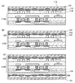
なお、図1においては、素子基板1102上に繊維体113を設けた後、有機樹脂層114を形成したが、この代わりに素子基板1102に有機樹脂層114を形成した後、繊維体を素子基板1102及び有機樹脂層114上に設けてもよい。この工程について、以下に示す。
In FIG. 1, the
図2(A)に示すように、半導体基板101上に単結晶半導体基板またはSOI基板を用いて素子基板1102を形成し、素子基板1102上にアンテナ112を形成する。次に、素子基板1102及びアンテナ112上に、有機樹脂層114を形成する。
As shown in FIG. 2A, an
次に、図2(B)に示すように、素子基板1102及びアンテナ112上に繊維体113を設ける。このとき、有機樹脂層114に繊維体113を押し付けることで、有機樹脂層114中に繊維体113を含ませることができる。また、繊維体113内に有機樹脂を含浸させることができる。
Next, as illustrated in FIG. 2B, the
次に、有機樹脂層114を加熱して、有機樹脂層114の有機樹脂を可塑化または硬化する。なお、有機樹脂が可塑性有機樹脂の場合、この後、室温に冷却することにより可塑化した有機樹脂を硬化する。
Next, the
この結果、図2(C)に示すように、繊維体113に含浸し、かつ素子基板1102及びアンテナ112の片面に固着される有機樹脂層121となる。なお、素子基板1102及びアンテナ112の片面に固着された有機樹脂層121及び繊維体113を、封止層120と示す。
As a result, as shown in FIG. 2C, the
この後、図1(D)と同様に、半導体基板101上に封止層129を形成してもよい。
After that, a
以上により、半導体装置を作製することができる。 Through the above steps, a semiconductor device can be manufactured.
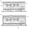
ここで、本実施の形態で示す半導体装置が有する効果について、図3を用いて示す。 Here, effects of the semiconductor device described in this embodiment are described with reference to FIGS.
図3(A)に示すように、従来の半導体装置40は、単結晶半導体基板またはSOI基板を用いて形成される半導体素子を含む素子基板41が接着材42a、42bを用いてフィルム43a、43bで封止される。このような半導体装置に局所的な押圧44を加える。
As shown in FIG. 3A, in a
その結果、図3(B)に示すように、素子基板41を構成する層、接着材42a、42b、フィルム43a、43bがそれぞれ延伸してしまい、押圧部において曲率半径の小さな湾曲が生じてしまう。この結果、素子基板41を構成する半導体素子、配線等に亀裂が生じてしまい、半導体装置が破壊されてしまう。
As a result, as shown in FIG. 3B, the layers constituting the
しかしながら、本実施の形態で示す半導体装置1050は、図3(C)に示すように、素子基板1051の片面または両面には、有機樹脂を含有する繊維体からなる封止層が設けられる。繊維体は高強度繊維で形成されており、高強度繊維は、引張弾性率またはヤング率が高い。このため、点圧や線圧等の局所的な押圧44がかかっても高強度繊維は延伸せず、押圧された力が繊維体全体に分散され、半導体装置全体で湾曲するようになる。この結果、図3(D)に示すように、局所的な押圧が加えられても、半導体装置で生じる湾曲は曲率半径の大きなものとなり、素子基板1051を構成する半導体素子、配線等に亀裂が生じず、半導体装置の破壊を低減することができる。
However, as shown in FIG. 3C, the
また、素子基板1051の厚さを薄くすることで、半導体装置を湾曲させることが可能となる。このため、素子基板1051の面積を大きくすることが可能である。このため、半導体装置を作製する工程が容易となる。また、当該半導体装置がアンテナ内蔵のRFIDの場合、アンテナのサイズを増大させることが可能である。このため、通信距離の長いRFIDを作製することができる。
Further, by reducing the thickness of the
なお、素子基板1102に複数の半導体装置が含まれる場合、素子基板1102及び封止層を分断して、複数の半導体装置を切り出してもよい。このような工程により、複数の半導体装置を作製することができる。分断する際は、ダイシング、スクライビング、はさみやナイフなどの刃物を有する裁断機、又はレーザーカット法等により選択的に分断することができる。
Note that in the case where the
また、半導体装置を紙に抄きこむことで、半導体装置を含む紙を形成することができる。具体的には、第1の湿紙上に半導体装置を設ける。その上に第2の湿紙を配置し、圧着及び乾燥する。この結果、半導体装置を含む紙を形成することができる。この後、当該紙を適当な大きさに切断してもよい。 In addition, paper containing a semiconductor device can be formed by paper-making the semiconductor device on paper. Specifically, a semiconductor device is provided over the first wet paper. A second wet paper is placed thereon, and is pressed and dried. As a result, paper including the semiconductor device can be formed. Thereafter, the paper may be cut into an appropriate size.
本実施の形態で示す半導体装置は、単結晶半導体基板またはSOI基板を用いて形成される半導体素子を有する素子基板と、繊維体とが有機樹脂で固着されている。繊維体は、局所的な押圧による圧力を繊維全体へ分散するため、局所的に圧力がかかりにくい。このため、半導体装置を構成する配線や半導体素子が延伸されず、半導体装置が破壊されにくい。即ち、素子基板に形成される半導体素子、配線等が延伸することを低減することができる。このため、歩留まりを向上させることができる。 In the semiconductor device described in this embodiment, an element substrate including a semiconductor element formed using a single crystal semiconductor substrate or an SOI substrate and a fibrous body are fixed with an organic resin. Since the fiber body disperses the pressure caused by local pressing throughout the fiber, it is difficult to apply pressure locally. For this reason, the wiring and semiconductor element which comprise a semiconductor device are not extended | stretched, and a semiconductor device is hard to be destroyed. That is, it is possible to reduce the stretching of the semiconductor elements, wirings, and the like formed on the element substrate. For this reason, a yield can be improved.
また、素子基板の厚さを薄くすることで、半導体装置を湾曲させることが可能となる。このため、素子基板の面積を大きくすることが可能である。このため、半導体装置を作製する工程が容易となる。また、当該半導体装置がアンテナ内蔵のRFIDの場合、アンテナのサイズを増大させることが可能である。このため、通信距離の長いRFIDを作製することができる。 In addition, the semiconductor device can be curved by reducing the thickness of the element substrate. For this reason, the area of the element substrate can be increased. For this reason, the process of manufacturing a semiconductor device becomes easy. In the case where the semiconductor device is an RFID with a built-in antenna, the size of the antenna can be increased. For this reason, an RFID having a long communication distance can be manufactured.
(実施の形態2)
本実施の形態では、実施の形態1と比較して、さらに破壊されにくい半導体装置の作製方法を図4を用いて説明する。
(Embodiment 2)
In this embodiment, a method for manufacturing a semiconductor device that is more unlikely to be broken than in
実施の形態1と同様に、図4(A)に示すように単結晶半導体基板またはSOI基板を用いて形成される半導体素子を含む素子基板1102及びアンテナ112を形成する。次に、素子基板1102及びアンテナ112上に繊維体113を設け、有機樹脂層114を形成し、有機樹脂層114上に保護フィルム131を設ける。
As in
保護フィルム131としては、高強度材料で形成されていることが好ましい。高強度材料の代表例としては、ポリビニルアルコール樹脂、ポリエステル樹脂、ポリアミド樹脂、ポリエチレン樹脂、アラミド樹脂、ポリパラフェニレンベンゾビスオキサゾール樹脂、ガラス樹脂等がある。
The
保護フィルム131が高強度材料で形成されていることで、実施の形態1と比較して局所的な押圧による破壊を抑制することができる。具体的には、繊維体113において、経糸束及び緯糸束が分布しないバスケットホールの面積が局所的圧力がかけられる面積より大きい場合、バスケットホールに局所的に荷重されると、当該圧力が繊維体113で吸収されず、直接素子基板1102及びアンテナ112にかかってしまう。この結果、素子基板1102及びアンテナ112が延伸し、半導体素子または配線が破壊されてしまう。
Since the
しかしながら、高強度材料で形成される保護フィルム131を有機樹脂層114上に設けることで、局所的な荷重を保護フィルム131全体で吸収するため、局所的な押圧による破壊の少ない半導体装置となる。
However, by providing the
次に、図4(B)に示すように、実施の形態1と同様に、有機樹脂層114を加熱して、封止層120を形成する。また、封止層120の有機樹脂は保護フィルム131を素子基板1102及びアンテナ112に固着する。即ち、封止層120は、繊維体113及び保護フィルム131を素子基板1102及びアンテナ112に固着している。また、封止層120に含まれる有機樹脂層121は繊維体113中に含浸される。
Next, as shown in FIG. 4B, the
次に、図4(C)に示すように、素子基板1102の半導体基板101に繊維体を設け、有機樹脂層を形成し、保護フィルム141を設け、加熱し圧着して封止層129により保護フィルム141を素子基板1102に固着してもよい。
Next, as illustrated in FIG. 4C, a fibrous body is provided over the
なお、図4(A)において、保護フィルム131が熱可塑性材料の場合、素子基板1102及びアンテナ112と繊維体113との間に保護フィルム131を設け加熱圧着してもよい。また、素子基板1102、アンテナ112及び繊維体113と、有機樹脂層114との間に保護フィルム131を設け加熱圧着してもよい。また、図4(C)において、保護フィルム141が熱可塑性材料の場合、素子基板1102と繊維体との間に保護フィルム141を設け加熱圧着してもよい。また、素子基板1102及び繊維体と、有機樹脂層との間に保護フィルム141を設け加熱圧着してもよい。当該構造においても、局所的押圧による荷重を保護フィルム及び繊維体で分散させることが可能であり、破壊を低減することができる。
Note that in FIG. 4A, in the case where the
なお、素子基板1102に複数の半導体装置が含まれる場合、素子基板1102及び封止層を分断して、複数の半導体装置を切り出してもよい。このような工程により、複数の半導体装置を作製することができる。
Note that in the case where the
また、実施の形態1と同様に、半導体装置を紙に抄きこむことで、半導体装置を含む紙を形成することができる。
Further, similarly to
以上により、局所的押圧による破壊が少ない半導体装置を作製することができる。また、素子基板の厚さを薄くすることで、半導体装置を湾曲させることが可能となる。このため、素子基板の面積を大きくすることが可能である。このため、半導体装置を作製する工程が容易となる。また、当該半導体装置がアンテナ内蔵のRFIDの場合、アンテナのサイズを増大させることが可能である。このため、通信距離の長いRFIDを作製することができる。 As described above, a semiconductor device with less damage due to local pressing can be manufactured. In addition, the semiconductor device can be curved by reducing the thickness of the element substrate. For this reason, the area of the element substrate can be increased. For this reason, the process of manufacturing a semiconductor device becomes easy. In the case where the semiconductor device is an RFID with a built-in antenna, the size of the antenna can be increased. For this reason, an RFID having a long communication distance can be manufactured.
(実施の形態3)
本実施の形態では、素子基板上にアンテナが形成されず、別の基板に設けられたアンテナを素子基板に接続した半導体装置の作製方法について、図5乃至図7を用いて説明する。
(Embodiment 3)
In this embodiment, a method for manufacturing a semiconductor device in which an antenna is not formed over an element substrate and an antenna provided over another substrate is connected to the element substrate will be described with reference to FIGS.
図5(A)に示すように、素子基板1151上に繊維体113及び開口部154を有する有機樹脂層155を形成する。
As shown in FIG. 5A, an
ここでは、素子基板1151としては、実施の形態1に示すように、半導体基板101にMOSトランジスタ1060a、1060bを形成する。MOSトランジスタ1060a、1060b上に絶縁層106を形成し、絶縁層106を介してMOSトランジスタソース領域及びドレイン領域に接続する導電層108、109を形成する。導電層108、109、絶縁層106上に絶縁層111を形成し、絶縁層111を介して導電層109と接続する電極パッド152を形成する。
Here, as the
有機樹脂層155は、電極パッド152の一部を露出するような開口部154を有するように有機樹脂を有機溶剤で希釈した組成物を印刷法または液滴吐出法により素子基板1151上に設け、乾燥焼成して形成する。
The
次に、図5(B)に示すように、有機樹脂層155の開口部に接続端子161を形成する。接続端子161は、印刷法、液滴吐出法等で形成することができる。接続端子161の材料としては、銀(Ag)、金(Au)、銅(Cu)、ニッケル(Ni)、白金(Pt)、パラジウム(Pd)、タンタル(Ta)、モリブデン(Mo)およびチタン(Ti)等のいずれか一つ以上の金属粒子やハロゲン化銀の微粒子、または分散性ナノ粒子を用いることができる。次に、接続端子の材料を焼成して、素子基板1151の片面に有機樹脂層155及び繊維体113からなる封止層156を形成する。なお、封止層156には、電極パッド152に接続する接続端子161が形成される。
Next, as illustrated in FIG. 5B, the
この後、図5(C)に示すように、素子基板1151に固着された封止層156と、アンテナ172が形成された基板171とを接着材174にて接着する。このとき、素子基板1151に形成された接続端子161とアンテナ172とを異方性導電接着材173を用いて電気的に接続する。
After that, as shown in FIG. 5C, the
異方性導電接着材173としては、分散した導電性粒子(粒径が、数nm〜数十μm)を含有する接着性樹脂であり、エポキシ樹脂、フェノール樹脂等が挙げられる。また、導電性粒子は、金、銀、銅、パラジウム、ニッケル、炭素、または白金から選ばれた一元素、若しくは複数の元素で形成される。また、これらの元素の多層構造を有する粒子でも良い。更には、樹脂で形成された粒子の表面に、金、銀、銅、パラジウム、ニッケル、または白金から選ばれた一元素、若しくは複数の元素で形成される薄膜が形成された導電性粒子を用いてもよい。さらには、導電性粒子として、CNT(カーボンナノチューブ)を用いてもよい。
The anisotropic
アンテナ172としては、実施の形態1に示すアンテナ112と同様の材料及び形成方法を適宜用いることができる。
As the
アンテナ172が形成された基板171としては、フィルム状のプラスチック基板、例えば、ポリエチレンテレフタレート(PET)、ポリエーテルスルホン(PES)、ポリエチレンナフタレート(PEN)、ポリカーボネート(PC)、ナイロン、ポリエーテルエーテルケトン(PEEK)、ポリスルホン(PSF)、ポリエーテルイミド(PEI)、ポリアリレート(PAR)、ポリブチレンテレフタレート(PBT)などを用いることができる。
As the
次に、図6(A)に示すように、実施の形態1と同様に、半導体基板101表面に封止層129を形成してもよい。
Next, as illustrated in FIG. 6A, a
次に、図6(B)に示すように、アンテナ172が形成される基板171と、封止層156、素子基板1151、及び封止層129を封止するようにフィルム175を設けてもよい。フィルムとしては、アンテナ172が形成された基板171と同様のフィルムを用いることができる。
Next, as illustrated in FIG. 6B, a
上記形態では、アンテナ172を有する基板171が素子基板1151の一方の面にのみ接着された半導体装置を示したが、素子基板1151の両面にそれぞれアンテナが形成された基板を接着してもよい。その形態を図7を用いて以下に示す。
Although the semiconductor device in which the
素子基板1181としては、実施の形態1に示すように、半導体基板101にMOSトランジスタ1060a、1060bを形成する。MOSトランジスタ1060a、1060b上に絶縁層106を形成し、絶縁層106を介してMOSトランジスタソース領域及びドレイン領域に接続する導電層108、109を形成する。導電層108、109、絶縁層106上に絶縁層111を形成し、絶縁層111を介して導電層109と接続する電極パッド152、及び導電層153を形成する。
As the
次に、半導体基板101、絶縁層106、絶縁層111に貫通孔を形成し、貫通孔の表面に貫通電極183を形成する。なお、貫通電極183は、導電層153に接する。また、貫通電極183は、絶縁層184によって、半導体基板101と絶縁されている。
Next, a through hole is formed in the
この後、当該素子基板1181の一表面に図5(A)及び(B)と同様の工程により、接続端子161を形成する。次に、図5(C)と同様の工程により、アンテナ172が形成された基板171と、素子基板1181の一方の面に設けられた封止層156とが接着材174で接着される。
After that, the
次に、素子基板1181の半導体基板101上に繊維体を設け、有機樹脂層を形成した後、加熱して、封止層125を形成する。次に、貫通電極183に接続する接続端子を形成するために、封止層125の一部に開口部を形成する。ここでは、封止層125から貫通電極183に至る開口部をレーザビーム照射により形成し、貫通電極183を一部露出する。
Next, a fibrous body is provided over the
次に、図7(B)に示すように、開口部を充填するように、接続端子186を形成する。接続端子186は、接続端子161と同様に形成することができる。
Next, as shown in FIG. 7B, a
次に、図7(C)に示すように、封止層129と、アンテナ192が形成された基板191を接着すると共に、接続端子186及びアンテナ192を異方性導電接着材193で電気的に接続する。
Next, as illustrated in FIG. 7C, the
以上により、素子基板の両面にアンテナが設けられた半導体装置を作製することができる。このような半導体装置は、UHF帯の電波受信可能なRFIDのように、対称構造のアンテナを有する半導体装置のときに用いると、半導体装置の大きさを小さくすることが可能であるため、好ましい。 As described above, a semiconductor device in which antennas are provided on both surfaces of an element substrate can be manufactured. Such a semiconductor device is preferably used for a semiconductor device having an antenna having a symmetrical structure, such as an RFID capable of receiving radio waves in the UHF band, because the size of the semiconductor device can be reduced.
なお、素子基板1151、1181に複数の半導体装置が含まれる場合、素子基板1151、1181及び封止層を分断して、複数の半導体装置を切り出してもよい。このような工程により、複数の半導体装置を作製することができる。
Note that in the case where the
また、実施の形態1と同様に、半導体装置を紙に抄きこむことで、半導体装置を含む紙を形成することができる。
Further, similarly to
本実施の形態で示す半導体装置は、単結晶半導体基板またはSOI基板を用いて形成される半導体素子を有する素子基板と、繊維体とが有機樹脂で固着されている。繊維体は、局所的な押圧による圧力を繊維全体へ分散するため、局所的に圧力がかかりにくい。このため、半導体装置を構成する配線や半導体素子が延伸されず、半導体装置が破壊されにくい。即ち、素子基板に形成される半導体素子、配線等が延伸することを低減することができる。このため、歩留まりを向上させることができる。 In the semiconductor device described in this embodiment, an element substrate including a semiconductor element formed using a single crystal semiconductor substrate or an SOI substrate and a fibrous body are fixed with an organic resin. Since the fiber body disperses the pressure caused by local pressing throughout the fiber, it is difficult to apply pressure locally. For this reason, the wiring and semiconductor element which comprise a semiconductor device are not extended | stretched, and a semiconductor device is hard to be destroyed. That is, it is possible to reduce the stretching of the semiconductor elements, wirings, and the like formed on the element substrate. For this reason, a yield can be improved.
また、素子基板の厚さを薄くすることで、半導体装置を湾曲させることが可能となる。このため、素子基板の面積を大きくすることが可能である。このため、外部アンテナを素子基板に接続する際、接続面積を大きくすることが可能となり、半導体装置を作製する工程が容易となる。また、当該半導体装置がアンテナ内蔵のRFIDの場合、アンテナのサイズを増大させることが可能である。このため、通信距離の長いRFIDを作製することができる。 In addition, the semiconductor device can be curved by reducing the thickness of the element substrate. For this reason, the area of the element substrate can be increased. For this reason, when the external antenna is connected to the element substrate, the connection area can be increased, and the process for manufacturing the semiconductor device is facilitated. In the case where the semiconductor device is an RFID with a built-in antenna, the size of the antenna can be increased. For this reason, an RFID having a long communication distance can be manufactured.
(実施の形態4)
本実施の形態では、実施の形態1乃至3で示す単結晶半導体基板またはSOI基板を用いて形成される半導体素子を含む素子基板がプリント基板に接続された半導体装置について、図10を用いて説明する。
(Embodiment 4)
In this embodiment, a semiconductor device in which an element substrate including a semiconductor element formed using the single crystal semiconductor substrate or the SOI substrate described in any of
図10(A)は、本実施の形態の半導体装置250の斜視図を示す。半導体装置250は、フレキシブルプリント基板に実施の形態1乃至3に示す単結晶半導体基板またはSOI基板を用いて形成される半導体素子を含む素子基板が設けられている。例えば、ポリエステル、ポリイミド等で形成されるベースフィルム251上に、銅、金、銀、アルミニウム等で形成される配線252が設けられる。また、配線252上に絶縁層を介して、実施の形態1乃至3に示す単結晶半導体基板またはSOI基板を用いて形成される半導体素子を含む素子基板及び封止層の積層体253a、253bが設けられている。また、配線252及び積層体253a、253bは、封止層のコンタクトホールに形成される接続端子を介して接続されている。ベースフィルム251、配線252、及び積層体253a、253bは、保護フィルム254で覆われている。また、半導体装置250の端部においては、保護フィルム254の一部が切除され、コネクタ等の外部回路と配線252が露出されている。
FIG. 10A shows a perspective view of the
素子基板を封止層を介してベース基板に設け、加熱圧着することで配線及びベース基板に素子基板を固着させることができる。 The element substrate can be fixed to the wiring and the base substrate by providing the element substrate on the base substrate with the sealing layer interposed therebetween and thermocompression bonding.
なお、ここでは、1層の配線252を有する半導体装置を示したが、この代わりに多層配線構造であってもよい。また、複数の配線で積層体253a、253bが挟まれていてもよい。このように配線を多層にすることで、実装密度を高めることが可能である。
Although a semiconductor device having one layer of
図10(B)は、本実施の形態の半導体装置260の断面図を示す。半導体装置260は、プリント基板に、実施の形態1乃至3に示す単結晶半導体基板またはSOI基板を用いて形成される半導体素子を含む素子基板が設けられている。例えば、コア層261の一方の面に実施の形態1乃至3に示す単結晶半導体基板またはSOI基板を用いて形成される半導体素子を含む素子基板262が設けられている。また、コア層261と、実施の形態1乃至3に示す単結晶半導体基板またはSOI基板を用いて形成される半導体素子を含む素子基板262に含まれる半導体素子または配線が、封止層263を貫通するビア264で接続される。
FIG. 10B is a cross-sectional view of the
また、素子基板262には多層配線265が設けられる。多層配線265の有機樹脂層266に形成されるビア267によって、コア層261、素子基板262に形成される半導体素子及び配線等が、半導体装置260表面に形成される導体パターン268と電気的に接続される。
The
また、コア層261の他方の面には多層配線269が設けられている。
A
また、半導体装置260に、コンデンサ、コイル、抵抗、ダイオード等のチップ271を導電性ペーストやワイヤー等の実装部材272で実装してもよい。
Further, a
本実施の形態の半導体装置は、プリント基板に単結晶半導体基板またはSOI基板を用いて形成される半導体素子を含む層を有する。また、繊維体を用いたプリプレグを用いて素子基板をプリント基板内に設ける。このため、局所的荷重(点圧、線圧等)がかかっても、繊維体で圧力が分散されるため、実装工程や湾曲による破壊を低減することができる。また、高集積化が可能である。
(実施の形態5)
The semiconductor device of this embodiment includes a layer including a semiconductor element formed using a single crystal semiconductor substrate or an SOI substrate on a printed board. Further, the element substrate is provided in the printed board using a prepreg using a fibrous body. For this reason, even if a local load (point pressure, linear pressure, etc.) is applied, the pressure is dispersed by the fibrous body, so that the breakage due to the mounting process or bending can be reduced. Further, high integration is possible.
(Embodiment 5)
本実施の形態では、本発明の半導体装置の構成及び応用例を示す。ここでは、半導体装置の代表例として、RFID及び記憶装置について説明する。 In this embodiment mode, a structure and an application example of a semiconductor device of the present invention are shown. Here, an RFID and a memory device will be described as typical examples of a semiconductor device.
はじめに、本発明の半導体装置の一つであるRFID501の回路構成例について説明する。図11に、RFID501の回路ブロック図を示す。
First, a circuit configuration example of an
図11のRFID501の仕様は、国際標準規格のISO15693に準拠し、近傍型で、交信信号周波数は13.56MHzである。また、受信はデータ読み出し命令のみ対応し、送信のデータ伝送レートは約13kHzであり、データ符号化形式はマンチェスタコードを用いている。
The specification of the
RFID501の回路部412は、大別して、電源部460、信号処理部461から構成される。電源部460は、整流回路462と保持容量463を有する。また、電源部460に、アンテナ411から受信した電力が過剰であった場合、内部回路を保護するための保護回路部(リミッタ回路部ともいう)と、保護回路部を動作させるかどうかを制御するための保護回路制御回路部とを設けてもよい。当該回路部を設けることにより、RFIDと通信機との通信距離が極端に短い状況等においてRFIDが大電力を受信することによって生じる不具合を防ぐことができ、RFIDの信頼性の向上を図ることができる。すなわち、RFID内部の素子の劣化や、RFID自体を破壊することなく、RFIDを正常に動作させることができる。
The circuit unit 412 of the
なお、ここでは、通信機とはRFIDと無線通信により情報の送受信を行う手段を有していればよく、例えば、情報を読み取るリーダや、読み取り機能及び書き込み機能を備えたリーダ/ライタ等が挙げられる。また、読み取り機能と書き込み機能の一方又は両方を備える携帯電話やコンピュータ等も含まれる。 Note that here, the communication device only needs to have means for transmitting and receiving information through RFID and wireless communication. For example, a reader that reads information, a reader / writer that has a reading function and a writing function, and the like can be given. It is done. In addition, a mobile phone, a computer, or the like having one or both of a reading function and a writing function is also included.
整流回路462は、アンテナ411で受信された搬送波を整流し、直流電圧を生成する。保持容量463は、整流回路462で生成された直流電圧を平滑化する。電源部460において生成された直流電圧は電源電圧として、信号処理部461の各回路に供給される。
The rectifier circuit 462 rectifies the carrier wave received by the
信号処理部461は、復調回路464、クロック生成/補正回路465、認識/判定回路466と、メモリコントローラ467、マスクROM468、符号化回路469、および変調回路470を有する。
The signal processing unit 461 includes a demodulation circuit 464, a clock generation / correction circuit 465, a recognition / determination circuit 466, a memory controller 467, a
復調回路464はアンテナで受信した信号を復調する回路である。復調回路464で復調された受信信号はクロック生成/補正回路465と認識/判定回路466に入力される。 The demodulation circuit 464 is a circuit that demodulates the signal received by the antenna. The received signal demodulated by the demodulation circuit 464 is input to the clock generation / correction circuit 465 and the recognition / determination circuit 466.
クロック生成/補正回路465は信号処理部461の動作に必要なクロック信号を生成し、さらにそれを補正する機能を有する。例えば、クロック生成/補正回路465は、電圧制御発振回路(以下VCO(Voltage Controlled Oscillator)回路)を有し、VCO回路の出力を帰還信号にして、供給される信号との位相を比較し、入力される信号と帰還信号が一定の位相になるよう負帰還により出力信号の調整を行う。 The clock generation / correction circuit 465 has a function of generating a clock signal necessary for the operation of the signal processing unit 461 and correcting it. For example, the clock generation / correction circuit 465 has a voltage controlled oscillation circuit (hereinafter referred to as a VCO (Voltage Controlled Oscillator) circuit), uses the output of the VCO circuit as a feedback signal, compares the phase with the supplied signal, The output signal is adjusted by negative feedback so that the received signal and the feedback signal have a constant phase.
認識/判定回路466は、命令コードを認識し判定する。認識/判定回路466が認識し、判定する命令コードは、フレーム終了信号(EOF、end of frame)、フレーム開始信号(SOF、start of frame)、フラグ、コマンドコード、マスク長(mask length)、マスク値(mask value)等である。また、認識/判定回路466は、送信エラーを識別する巡回冗長検査(CRC、cyclic redundancy check)機能も含む。 The recognition / determination circuit 466 recognizes and determines the instruction code. The instruction code recognized and determined by the recognition / determination circuit 466 includes a frame end signal (EOF, end of frame), a frame start signal (SOF), a flag, a command code, a mask length (mask length), and a mask. For example, a value (mask value). The recognition / determination circuit 466 also includes a cyclic redundancy check (CRC) function for identifying a transmission error.
メモリコントローラ467は、認識/判定回路466で処理された信号を基に、マスクROMからデータを読み出す。また、マスクROM468は、IDなどが記憶されている。マスクROM468を搭載することで、複製や改ざんが不可能な読み取り専用のRFID501として構成される。このような読み取り専用のRFID501を紙に抄き込むことで、偽造防止の紙を提供することができる。
The memory controller 467 reads data from the mask ROM based on the signal processed by the recognition / determination circuit 466. The
符号化回路469はメモリコントローラ467がマスクROM468から読み出したデータを符号化する。符号化されたデータは変調回路470で変調される。変調回路470で変調されたデータはアンテナ411から搬送波に重畳させて送信される。
The
次に、RFIDの使用例について示す。本発明のRFIDはあらゆる紙媒体及びフィルム媒体に使用できる。特に、本発明のRFIDは、偽造防止が要求されるあらゆる紙媒体に使用することができる。例えば、紙幣、戸籍謄本、住民票、パスポート、免許証、身分証、会員証、鑑定書、診察券、定期券、手形、小切手、貨物引換証、船貨証券、倉庫証券、株券、債券、商品券、チケット、抵当証券などである。 Next, an example of using RFID will be described. The RFID of the present invention can be used for any paper and film media. In particular, the RFID of the present invention can be used for any paper medium that requires anti-counterfeiting. For example, banknotes, certified copy of family register, resident's card, passport, license, identification card, membership card, certificate, examination ticket, commuter pass, bill, check, cargo voucher, cargo bill, warehouse securities, stock certificate, bond, product Tickets, tickets, mortgage securities, etc.
また、本発明の実施により、紙媒体上で視覚的に示される情報以上の多くの情報を紙媒体及びフィルム媒体に持たせることができるため、本発明のRFIDを商品ラベルなどに適用することで、商品の管理の電子システム化や、商品の盗難の防止に利用できる。以下、図12を用いて、本発明に係る紙の使用例を説明する。 In addition, by implementing the present invention, it is possible to give the paper medium and film medium more information than the information visually shown on the paper medium. Therefore, by applying the RFID of the present invention to a product label or the like, It can be used for electronic management of merchandise management and prevention of merchandise theft. Hereinafter, an example of using the paper according to the present invention will be described with reference to FIG.
図12(A)は、本発明のRFID501を抄き込んだ紙を使用した無記名債券類511の一例である。無記名債券類511には、切手、切符、チケット、入場券、商品券、図書券、文具券、ビール券、おこめ券、各種ギフト券、各種サービス券等が含まれるが、勿論これらに限定されるものではない。また、図12(B)は、本発明に係るRFID501を抄き込んだ紙を使用した証書類512(例えば、住民票、戸籍謄本)の一例である。
FIG. 12A is an example of
図12(C)は、本発明のRFIDをラベルに適用した一例である。ラベル台紙(セパレート紙)513上に、RFID501が抄き込まれた紙でラベル(IDシール)514が形成されている。ラベル514は、ボックス515内に収納されている。ラベル514上には、その商品や役務に関する情報(商品名、ブランド、商標、商標権者、販売者、製造者等)が印刷されている。さらに、RFID501には、その商品(又は商品の種類)固有のIDナンバーが記憶されているため、偽造や、商標権、特許権等の知的財産権侵害、不正競争等の不法行為を容易に把握することができる。RFID501には、商品の容器やラベルに明記しきれない多大な情報、例えば、商品の産地、販売地、品質、原材料、効能、用途、数量、形状、価格、生産方法、使用方法、生産時期、使用時期、賞味期限、取扱説明、商品に関する知的財産情報等を入力しておくことができる。そのため、取引者や消費者は、簡易な通信機によって、それらの情報にアクセスすることができる。また、生産者側からは容易に書換え、消去等も可能であるが、取引者、消費者側からは書換え、消去等ができない仕組みになっている。
FIG. 12C illustrates an example in which the RFID of the present invention is applied to a label. On a label mount (separate paper) 513, a label (ID seal) 514 is formed of paper on which the
図12(D)は、RFID501を抄き込んだ紙またはフィルムでなるタグ516を示している。RFID501を抄き込んだ紙またはフィルムでタグ516を作製することで、プラスチックの筐体を使用した従来のIDタグよりも安価に製造することができる。図12(E)は、本発明のRFIDを表紙に用いた書籍517であり、表紙にRFID501が抄き込まれている。
FIG. 12D illustrates a
本発明の半導体装置の一例であるRFIDを搭載したラベル514やタグ516を商品に取り付けておくことで、商品管理が容易になる。例えば、商品が盗難された場合に、商品の経路を辿ることによって、その犯人を迅速に把握することができる。このように、本発明のRFIDをIDタグとして用いることで、商品の原材料や産地、製造や加工、流通、販売などに至るまでの履歴管理や、追跡照会を可能にする。すなわち、商品のトレーサビリティを可能にする。また、本発明により、商品のトレーサビリティ管理システムを従来よりも低コストで導入をすることを可能する。
Commodity management is facilitated by attaching a
また、本発明の半導体装置の一例であるRFIDは、局所的押圧により破壊しにくい。このため、本発明の半導体装置の一例であるRFIDを有する紙媒体及びフィルム媒体は、貼り付けや設置等の処理において、湾曲させることが可能であり、処理効率が高まる。また、本発明の半導体装置の一例であるRFIDを有する紙媒体及びフィルム媒体に筆記用具で情報を記入することが可能であるため、用途範囲が広がる。 Further, the RFID which is an example of the semiconductor device of the present invention is not easily destroyed by local pressing. For this reason, a paper medium and a film medium having an RFID, which is an example of the semiconductor device of the present invention, can be bent in processing such as attachment and installation, and processing efficiency is increased. In addition, since it is possible to write information on a paper medium and a film medium having an RFID, which is an example of the semiconductor device of the present invention, with a writing tool, the application range is widened.
次に、本発明の半導体装置の一形態である記憶装置の構成について、以下に示す。ここでは記憶装置の代表例として不揮発性記憶装置を用いて示す。 Next, a structure of a memory device which is one embodiment of the semiconductor device of the present invention is described below. Here, a nonvolatile memory device is used as a representative example of the memory device.
図13は、不揮発性半導体記憶装置の回路ブロック図の一例を示している。不揮発性半導体記憶装置は、メモリセルアレイ552と周辺回路554が同一の素子基板上に形成されている。メモリセルアレイ552は、実施の形態1で示すような不揮発性記憶素子を有している。周辺回路554の構成は以下の通りである。
FIG. 13 shows an example of a circuit block diagram of a nonvolatile semiconductor memory device. In the nonvolatile semiconductor memory device, the
ワード線選択のためにロウデコーダ562と、ビット線選択のためにカラムデコーダ564が、メモリセルアレイ552の周囲に設けられている。アドレスは、アドレスバッファ556を介してコントロール回路558に送られ、内部ロウアドレス信号及び内部カラムアドレス信号がそれぞれロウデコーダ562及びカラムデコーダ564に転送される。
A
データ書き込み及び消去には、電源電位を昇圧した電位が用いられる。このため、コントロール回路558により動作モードに応じて制御される昇圧回路560が設けられている。昇圧回路560の出力はロウデコーダ562やカラムデコーダ564を介して、ワード線やビット線に供給される。センスアンプ566はカラムデコーダ564から出力されたデータが入力される。センスアンプ566により読み出されたデータは、データバッファ568に保持され、コントロール回路558からの制御により、データがランダムアクセスされ、データ入出力バッファ570を介して出力されるようになっている。書き込みデータは、データ入出力バッファ570を介してデータバッファ568に一旦保持され、コントロール回路558の制御によりカラムデコーダ564に転送される。
For writing and erasing data, a potential obtained by boosting the power supply potential is used. For this reason, a
このように、不揮発性半導体記憶装置では、メモリセルアレイ552において、電源電位とは異なる電位を用いる必要がある。そのため、少なくともメモリセルアレイ552と周辺回路554の間は、電気的に絶縁分離されていることが望ましい。この場合、不揮発性記憶素子及び周辺回路のトランジスタを絶縁表面に形成した単結晶半導体層で形成することにより、容易に絶縁分離をすることができる。それにより、誤動作を無くし、消費電力の低い不揮発性半導体記憶装置を得ることができる。
(実施の形態6)
As described above, in the nonvolatile semiconductor memory device, it is necessary to use a potential different from the power supply potential in the
(Embodiment 6)
本実施の形態では、本発明の半導体装置を用いた電子機器について以下に示す。 In this embodiment mode, electronic devices using the semiconductor device of the present invention are described below.
本発明の半導体装置を適用した電子機器として、ビデオカメラ、デジタルカメラ等のカメラ、ゴーグル型ディスプレイ(ヘッドマウントディスプレイ)、ナビゲーションシステム、音響再生装置(カーオーディオ、オーディオコンポ等)、コンピュータ、ゲーム機器、携帯情報端末(モバイルコンピュータ、携帯電話、携帯型ゲーム機または電子書籍等)、記録媒体を備えた画像再生装置(具体的にはDVD(digital versatile disc)等の記録媒体を再生し、その画像を表示しうるディスプレイを備えた装置)などが挙げられる。それら電子機器の具体例を図14に示す。 As electronic devices to which the semiconductor device of the present invention is applied, cameras such as video cameras and digital cameras, goggle type displays (head mounted displays), navigation systems, sound playback devices (car audio, audio components, etc.), computers, game machines, Play back a recording medium such as a portable information terminal (mobile computer, mobile phone, portable game machine or electronic book), an image playback device (specifically a DVD (digital versatile disc)) equipped with a recording medium, A device having a display capable of displaying). Specific examples of these electronic devices are shown in FIGS.
図14(A)、(B)は、デジタルカメラを示している。図14(B)は、図14(A)の裏側を示す図である。このデジタルカメラは、筐体2111、表示部2112、レンズ2113、操作キー2114、シャッターボタン2115などを有する。筐体2111内部には、記憶装置、MPU、イメージセンサ等の機能を有する本発明の半導体装置2116を備えている。
14A and 14B show a digital camera. FIG. 14B is a diagram showing the back side of FIG. This digital camera includes a
また、図14(C)は、携帯電話を示しており、携帯端末の1つの代表例である。この携帯電話は筐体2121、表示部2122、操作キー2123などを含む。また、携帯電話の内部には、記憶装置、MPU、イメージセンサ等の機能を有する本発明の半導体装置2125を備えている。
FIG. 14C illustrates a mobile phone, which is a typical example of a mobile terminal. This mobile phone includes a
また、図14(D)は、デジタルプレーヤーを示しており、オーディオ装置の1つの代表例である。図14(D)に示すデジタルプレーヤーは、本体2130、表示部2131、記憶装置、MPU、イメージセンサ等の機能を有する本発明の半導体装置2132、操作部2133、イヤホン2134等を含んでいる。
FIG. 14D illustrates a digital player, which is a typical example of an audio device. A digital player shown in FIG. 14D includes a
また、図14(E)は、電子ブック(電子ペーパーともいう)を示している。この電子ブックは、本体2141、表示部2142、操作キー2143、記憶装置、MPU、イメージセンサ等の機能を有する本発明の半導体装置2144を含んでいる。またモデムが本体2141に内蔵されていてもよいし、無線で情報を送受信できる構成としてもよい。
FIG. 14E illustrates an electronic book (also referred to as electronic paper). This electronic book includes a
以上の様に、本発明の半導体装置の適用範囲は極めて広く、他の電子機器に用いることが可能である。 As described above, the applicable range of the semiconductor device of the present invention is so wide that the semiconductor device can be used for other electronic devices.
Claims (12)
前記素子基板上に繊維体を設け、前記繊維体及び前記素子基板上から有機樹脂を含む組成物を塗布した後、加熱して、前記素子基板上に前記繊維体及び前記繊維体に含浸された有機樹脂を含む封止層を形成することを特徴とする半導体装置の作製方法。 Forming an active element formed using a single crystal semiconductor substrate or an SOI substrate and an element substrate having an insulating layer covering the active element;
A fiber body is provided on the element substrate, a composition containing an organic resin is applied from the fiber body and the element substrate, and then heated to impregnate the fiber body and the fiber body on the element substrate. A method for manufacturing a semiconductor device, comprising forming a sealing layer containing an organic resin.
前記素子基板の一方の面に第1の繊維体を設け、前記第1の繊維体及び前記素子基板上から第1の有機樹脂を含む組成物を塗布した後、加熱して、前記素子基板上に前記第1の繊維体及び前記第1の繊維体に含浸された第1の有機樹脂を含む第1の封止層を形成し、
第2の繊維体を前記素子基板の他方の面に設け、前記第2の繊維体及び前記素子基板上から第2の有機樹脂を含む組成物を塗布した後、加熱して、前記素子基板上に前記第2の繊維体及び前記第2の繊維体に含浸された第2の有機樹脂を含む第2の封止層を形成することを特徴とする半導体装置の作製方法。 Forming an active element formed using a single crystal semiconductor substrate or an SOI substrate and an element substrate having an insulating layer covering the active element;
A first fibrous body is provided on one surface of the element substrate, and a composition containing a first organic resin is applied from the first fibrous body and the element substrate, and then heated to form the first substrate on the element substrate. Forming a first sealing layer containing the first fibrous body and the first organic resin impregnated in the first fibrous body;
A second fibrous body is provided on the other surface of the element substrate, a composition containing a second organic resin is applied from above the second fibrous body and the element substrate, and then heated, on the element substrate. And forming a second sealing layer containing the second fibrous body and a second organic resin impregnated in the second fibrous body.
前記素子基板上に有機樹脂層を形成し、前記有機樹脂層及び前記素子基板上に繊維体を設けた後、加熱して、前記素子基板上に前記繊維体及び前記繊維体に含浸された有機樹脂を含む封止層を形成することを特徴とする半導体装置の作製方法。 Forming an active element formed using a single crystal semiconductor substrate or an SOI substrate and an element substrate having an insulating layer covering the active element;
An organic resin layer is formed on the element substrate, a fiber body is provided on the organic resin layer and the element substrate, and then heated, and the fiber body and the fiber body impregnated on the element substrate are heated. A method for manufacturing a semiconductor device, wherein a sealing layer containing a resin is formed.
前記素子基板上に第1の有機樹脂層を形成し、前記第1の有機樹脂層及び前記素子基板上に第1の繊維体を設けた後、加熱して、前記素子基板上に前記第1の繊維体及び前記第1の繊維体に含浸された第1の有機樹脂を含む第1の封止層を形成し、
第2の有機樹脂層を前記素子基板の他方の面に形成し、前記第2の有機樹脂層及び前記素子基板上に第2の繊維体を設けた後、加熱して、前記素子基板上に前記第2の繊維体及び前記第2の繊維体に含浸された第2の有機樹脂を含む第2の封止層を形成することを特徴とする半導体装置の作製方法。 Forming an active element formed using a single crystal semiconductor substrate or an SOI substrate and an element substrate having an insulating layer covering the active element;
A first organic resin layer is formed on the element substrate, a first fibrous body is provided on the first organic resin layer and the element substrate, and then heated to heat the first organic resin layer on the element substrate. Forming a first sealing layer containing the first organic resin impregnated with the fiber body and the first fiber body,
A second organic resin layer is formed on the other surface of the element substrate, a second fibrous body is provided on the second organic resin layer and the element substrate, and then heated to form on the element substrate. A method for manufacturing a semiconductor device, comprising: forming a second sealing layer including the second fibrous body and a second organic resin impregnated in the second fibrous body.
前記素子基板上に繊維体を設け、前記繊維体及び前記素子基板上から有機樹脂を含む組成物を塗布した後、加熱して、前記素子基板上に前記繊維体及び前記繊維体に含浸された有機樹脂を含む封止層を形成し、
前記封止層の開口部に前記配線に接続する接続端子を形成し、
前記封止層にアンテナを有する基板を貼り付けると共に、前記接続端子及び前記アンテナを電気的に接続することを特徴とする半導体装置の作製方法。 Forming an active element formed using a single crystal semiconductor substrate or an SOI substrate, an insulating layer covering the active element, and an element substrate having wiring;
A fiber body is provided on the element substrate, a composition containing an organic resin is applied from the fiber body and the element substrate, and then heated to impregnate the fiber body and the fiber body on the element substrate. Forming a sealing layer containing an organic resin;
Forming a connection terminal connected to the wiring in the opening of the sealing layer;
A method for manufacturing a semiconductor device, wherein a substrate having an antenna is attached to the sealing layer, and the connection terminal and the antenna are electrically connected.
前記素子基板の一方の面に第1の繊維体を設け、前記第1の繊維体及び前記素子基板上から第1の有機樹脂を含む組成物を塗布した後加熱して、前記素子基板上に前記第1の繊維体及び前記第1の繊維体に含浸された前記第1の有機樹脂を含む第1の封止層を形成し、前記第1の封止層の開口部に前記配線に接続する接続端子を形成し、
前記第1の封止層にアンテナを有する基板を貼り付けると共に、前記接続端子及び前記アンテナを電気的に接続し、
第2の繊維体を前記素子基板の他方の面に設け、前記第2の繊維体及び前記素子基板上から第2の有機樹脂を含む組成物を塗布した後、加熱して、前記素子基板上に前記第2の繊維体及び前記第2の繊維体に含浸された第2の有機樹脂を含む第2の封止層を形成することを特徴とする半導体装置の作製方法。 Forming an active element formed using a single crystal semiconductor substrate or an SOI substrate, an insulating layer covering the active element, and an element substrate having wiring;
A first fibrous body is provided on one surface of the element substrate, a composition containing a first organic resin is applied from above the first fibrous body and the element substrate, and then heated, on the element substrate. Forming a first sealing layer containing the first fibrous body and the first organic resin impregnated in the first fibrous body, and connecting the wiring to an opening of the first sealing layer; Forming connection terminals to
Affixing a substrate having an antenna on the first sealing layer, electrically connecting the connection terminal and the antenna,
A second fibrous body is provided on the other surface of the element substrate, a composition containing a second organic resin is applied from above the second fibrous body and the element substrate, and then heated, on the element substrate. And forming a second sealing layer containing the second fibrous body and a second organic resin impregnated in the second fibrous body.
前記素子基板の一方の面に第1の繊維体を設け、前記第1の繊維体及び前記素子基板上から前記第1の配線の一部を露出する開口部を有する第1の有機樹脂層を含む組成物を塗布した後、加熱して、前記素子基板上に前記第1の繊維体及び前記第1の繊維体に含浸された第1の有機樹脂を含む第1の封止層を形成し、前記第1の封止層の開口部に前記第1の配線に接続する第1の接続端子を形成し、
前記第1の封止層に第1のアンテナを有する基板を貼り付けると共に、前記第1の接続端子及び前記第1のアンテナを電気的に接続し、
第2の繊維体を前記素子基板の他方の面に設け、前記第2の繊維体及び前記素子基板上から第2の有機樹脂を含む組成物を塗布した後、加熱して、前記素子基板上に前記第2の繊維体及び前記第2の繊維体に含浸された第2の有機樹脂を含む第2の封止層を形成した後、前記第2の配線の一部を露出する開口部を形成し、前記第2の有機樹脂層の開口部に前記第2の配線に接続する第2の接続端子を形成し、
前記第2の封止層に第2のアンテナを有する基板を貼り付けると共に、前記第2の接続端子及び前記第2のアンテナを電気的に接続することを特徴とする半導体装置の作製方法。 Forming an active element formed using a single crystal semiconductor substrate or an SOI substrate, an insulating layer covering the active element, a first wiring, and an element substrate having a second wiring;
A first fibrous body is provided on one surface of the element substrate, and a first organic resin layer having an opening that exposes a part of the first wiring from the first fibrous body and the element substrate. After applying the composition containing heat, it is heated to form a first sealing layer containing the first fibrous body and the first organic resin impregnated in the first fibrous body on the element substrate. Forming a first connection terminal connected to the first wiring in the opening of the first sealing layer;
Affixing a substrate having a first antenna on the first sealing layer, electrically connecting the first connection terminal and the first antenna,
A second fibrous body is provided on the other surface of the element substrate, a composition containing a second organic resin is applied from above the second fibrous body and the element substrate, and then heated, on the element substrate. Forming a second sealing layer including the second fibrous body and the second organic resin impregnated in the second fibrous body, and then opening an opening exposing a part of the second wiring. Forming a second connection terminal connected to the second wiring in the opening of the second organic resin layer;
A method for manufacturing a semiconductor device, wherein a substrate having a second antenna is attached to the second sealing layer, and the second connection terminal and the second antenna are electrically connected to each other.
前記素子基板上に前記配線の一部を露出する開口部を有する有機樹脂層を形成し、前記有機樹脂層及び前記素子基板上に繊維体を設けた後、加熱して、前記素子基板上に前記繊維体及び前記繊維体に含浸された有機樹脂を含む封止層を形成し、前記有機樹脂層の開口部に前記配線に接続する接続端子を形成し、
前記封止層にアンテナを有する基板を貼り付けると共に、前記接続端子及び前記アンテナを電気的に接続することを特徴とする半導体装置の作製方法。 Forming an active element formed using a single crystal semiconductor substrate or an SOI substrate, an insulating layer covering the active element, and an element substrate having wiring;
An organic resin layer having an opening that exposes a part of the wiring is formed on the element substrate, a fiber body is provided on the organic resin layer and the element substrate, and then heated to form on the element substrate. Forming a sealing layer containing an organic resin impregnated in the fibrous body and the fibrous body, forming a connection terminal connected to the wiring in an opening of the organic resin layer;
A method for manufacturing a semiconductor device, wherein a substrate having an antenna is attached to the sealing layer, and the connection terminal and the antenna are electrically connected.
前記素子基板の一方の面に前記配線の一部を露出する開口部を有する第1の有機樹脂層を形成し、前記第1の機樹脂層及び前記素子基板上に第1の繊維体を設けた後加熱して、前記素子基板上に前記第1の繊維体及び前記第1の繊維体に含浸された第1の有機樹脂を含む第1の封止層を形成し、前記第1の有機樹脂層の開口部に前記配線に接続する接続端子を形成し、
前記第1の封止層にアンテナを有する基板を貼り付けると共に、前記接続端子及び前記アンテナを電気的に接続し、
第2の有機樹脂層を前記素子基板の他方の面に形成し、前記第2の有機樹脂層及び前記素子基板上に第2の繊維体を設けた後、加熱して、前記素子基板上に前記第2の繊維体及び前記第2の繊維体に含浸された第2の有機樹脂を含む第2の封止層を形成することを特徴とする半導体装置の作製方法。 Forming an active element formed using a single crystal semiconductor substrate or an SOI substrate, an insulating layer covering the active element, and an element substrate having wiring;
A first organic resin layer having an opening exposing a part of the wiring is formed on one surface of the element substrate, and a first fibrous body is provided on the first machine resin layer and the element substrate. And then heating to form a first sealing layer containing the first fibrous body and the first organic resin impregnated in the first fibrous body on the element substrate, and the first organic A connection terminal connected to the wiring is formed in the opening of the resin layer,
Affixing a substrate having an antenna on the first sealing layer, electrically connecting the connection terminal and the antenna,
A second organic resin layer is formed on the other surface of the element substrate, a second fibrous body is provided on the second organic resin layer and the element substrate, and then heated to form on the element substrate. A method for manufacturing a semiconductor device, comprising: forming a second sealing layer including the second fibrous body and a second organic resin impregnated in the second fibrous body.
前記第1の封止層に第1のアンテナを有する基板を貼り付けると共に、前記第1の接続端子及び前記第1のアンテナを電気的に接続し、
前記素子基板の他方の面に第2の有機樹脂層を形成し、前記第2の有機樹脂層及び前記素子基板上に第2の繊維体を設けた後、加熱して、前記素子基板上に前記第2の繊維体及び前記第2の繊維体に含浸された第2の有機樹脂を含む第2の封止層を形成した後、前記第2の配線の一部を露出する開口部を形成し、前記第2の有機樹脂層の開口部に前記第2の配線に接続する第2の接続端子を形成し、
前記第2の封止層に第2のアンテナを有する基板を貼り付けると共に、前記第2の接続端子及び前記第2のアンテナを電気的に接続することを特徴とする半導体装置の作製方法。 An element substrate having an active element formed using a single crystal semiconductor substrate or an SOI substrate, an insulating layer covering the active element, a first wiring, and a second wiring is formed, and the first substrate is formed on the element substrate. Forming a first organic resin layer having an opening exposing a part of the wiring, forming a first fibrous body on the first organic resin layer and the element substrate, and heating the Forming a first sealing layer including the first fibrous body and the first organic resin impregnated in the first fibrous body on the element substrate; and opening the first organic resin layer to the opening portion of the first organic resin layer. Forming a first connection terminal connected to the first wiring;
Affixing a substrate having a first antenna on the first sealing layer, electrically connecting the first connection terminal and the first antenna,
A second organic resin layer is formed on the other surface of the element substrate, a second fibrous body is provided on the second organic resin layer and the element substrate, and then heated to form on the element substrate. After forming the second sealing body containing the second fibrous body and the second organic resin impregnated in the second fibrous body, an opening for exposing a part of the second wiring is formed. And forming a second connection terminal connected to the second wiring in the opening of the second organic resin layer,
A method for manufacturing a semiconductor device, wherein a substrate having a second antenna is attached to the second sealing layer, and the second connection terminal and the second antenna are electrically connected to each other.
Priority Applications (1)
| Application Number | Priority Date | Filing Date | Title |
|---|---|---|---|
| JP2008062132A JP2008270762A (en) | 2007-03-26 | 2008-03-12 | Method of manufacturing semiconductor device |
Applications Claiming Priority (2)
| Application Number | Priority Date | Filing Date | Title |
|---|---|---|---|
| JP2007079264 | 2007-03-26 | ||
| JP2008062132A JP2008270762A (en) | 2007-03-26 | 2008-03-12 | Method of manufacturing semiconductor device |
Publications (2)
| Publication Number | Publication Date |
|---|---|
| JP2008270762A true JP2008270762A (en) | 2008-11-06 |
| JP2008270762A5 JP2008270762A5 (en) | 2011-03-17 |
Family
ID=39643903
Family Applications (1)
| Application Number | Title | Priority Date | Filing Date |
|---|---|---|---|
| JP2008062132A Withdrawn JP2008270762A (en) | 2007-03-26 | 2008-03-12 | Method of manufacturing semiconductor device |
Country Status (6)
| Country | Link |
|---|---|
| US (1) | US7785933B2 (en) |
| EP (1) | EP1976000A3 (en) |
| JP (1) | JP2008270762A (en) |
| KR (1) | KR101466594B1 (en) |
| CN (1) | CN101276767B (en) |
| TW (1) | TWI442513B (en) |
Cited By (4)
| Publication number | Priority date | Publication date | Assignee | Title |
|---|---|---|---|---|
| JP2011244111A (en) * | 2010-05-14 | 2011-12-01 | Murata Mfg Co Ltd | Wireless ic device |
| US8710683B2 (en) | 2010-09-29 | 2014-04-29 | Samsung Electronics Co., Ltd. | Method of forming wafer level mold using glass fiber and wafer structure formed by the same |
| KR20150014563A (en) * | 2013-07-29 | 2015-02-09 | 삼성디스플레이 주식회사 | Thin film transistor substrate, method of manufacturing the same and display device comprising the same |
| KR101821861B1 (en) | 2015-10-15 | 2018-01-25 | 한국과학기술원 | Wearable memory with textile substrate and manufacturing method thereof |
Families Citing this family (29)
| Publication number | Priority date | Publication date | Assignee | Title |
|---|---|---|---|---|
| KR101478810B1 (en) | 2006-07-28 | 2015-01-02 | 가부시키가이샤 한도오따이 에네루기 켄큐쇼 | Power storage device |
| EP1970952A3 (en) | 2007-03-13 | 2009-05-06 | Semiconductor Energy Laboratory Co., Ltd. | Semiconductor device and manufacturing method thereof |
| EP1970951A3 (en) * | 2007-03-13 | 2009-05-06 | Semiconductor Energy Laboratory Co., Ltd. | Semiconductor device and manufacturing method thereof |
| JP5268395B2 (en) * | 2007-03-26 | 2013-08-21 | 株式会社半導体エネルギー研究所 | Method for manufacturing semiconductor device |
| JP2009205669A (en) * | 2008-01-31 | 2009-09-10 | Semiconductor Energy Lab Co Ltd | Semiconductor device |
| JP5473413B2 (en) | 2008-06-20 | 2014-04-16 | 株式会社半導体エネルギー研究所 | Wiring substrate manufacturing method, antenna manufacturing method, and semiconductor device manufacturing method |
| US8563397B2 (en) * | 2008-07-09 | 2013-10-22 | Semiconductor Energy Laboratory Co., Ltd. | Semiconductor device and manufacturing method thereof |
| KR101588576B1 (en) | 2008-07-10 | 2016-01-26 | 가부시키가이샤 한도오따이 에네루기 켄큐쇼 | Light emitting device and electronic device |
| JP5358324B2 (en) * | 2008-07-10 | 2013-12-04 | 株式会社半導体エネルギー研究所 | Electronic paper |
| JP2010041040A (en) * | 2008-07-10 | 2010-02-18 | Semiconductor Energy Lab Co Ltd | Photoelectric conversion device and method of manufacturing the same |
| WO2010035627A1 (en) * | 2008-09-25 | 2010-04-01 | Semiconductor Energy Laboratory Co., Ltd. | Semiconductor device |
| JP5583951B2 (en) * | 2008-11-11 | 2014-09-03 | 株式会社半導体エネルギー研究所 | Method for manufacturing semiconductor device |
| JP5470054B2 (en) * | 2009-01-22 | 2014-04-16 | 株式会社半導体エネルギー研究所 | Semiconductor device |
| GB2469628A (en) * | 2009-04-20 | 2010-10-27 | Michael Edward Beese | Two Part Identification Label |
| KR101732397B1 (en) * | 2009-06-05 | 2017-05-04 | 가부시키가이샤 한도오따이 에네루기 켄큐쇼 | Photoelectric conversion device and manufacturing method thereof |
| WO2010140539A1 (en) * | 2009-06-05 | 2010-12-09 | Semiconductor Energy Laboratory Co., Ltd. | Photoelectric conversion device and method for manufacturing the same |
| KR101677076B1 (en) * | 2009-06-05 | 2016-11-17 | 가부시키가이샤 한도오따이 에네루기 켄큐쇼 | Photoelectric conversion device and method for manufacturing the same |
| US8345435B2 (en) * | 2009-08-07 | 2013-01-01 | Semiconductor Energy Laboratory Co., Ltd. | Terminal structure and manufacturing method thereof, and electronic device and manufacturing method thereof |
| JP5719560B2 (en) * | 2009-10-21 | 2015-05-20 | 株式会社半導体エネルギー研究所 | Manufacturing method of terminal structure |
| CN102403225B (en) * | 2010-09-07 | 2013-08-14 | 无锡华润上华半导体有限公司 | Manufacturing method and device of channel double-diffusion metal oxide semiconductor |
| US8518798B2 (en) * | 2010-09-23 | 2013-08-27 | Infineon Technologies Ag | Semiconductor structure and method for making same |
| WO2012070035A1 (en) * | 2010-11-26 | 2012-05-31 | The National Microelectronics Applications Centre Limited | An ac current or voltage sensor |
| US20130229776A1 (en) * | 2011-12-23 | 2013-09-05 | Wisconsin Alumni Research Foundation | High-speed, flexible integrated circuits and methods for making high-speed, flexible integrated circuits |
| JP2014135422A (en) * | 2013-01-11 | 2014-07-24 | Toyota Motor Corp | Semiconductor device manufacturing method |
| KR102086098B1 (en) * | 2013-07-03 | 2020-03-09 | 삼성디스플레이 주식회사 | Display device |
| KR101418974B1 (en) * | 2014-01-23 | 2014-07-14 | 김용석 | Protective film management system for smart phone |
| US20170170016A1 (en) * | 2015-12-14 | 2017-06-15 | Globalfoundries Inc. | Multiple patterning method for substrate |
| DE102016107678B4 (en) * | 2016-04-26 | 2023-12-28 | Infineon Technologies Ag | SEMICONDUCTOR DEVICES WITH ON-CHIP ANTENNAS AND THEIR PRODUCTION |
| JP6577910B2 (en) * | 2016-06-23 | 2019-09-18 | ルネサスエレクトロニクス株式会社 | Electronic equipment |
Citations (7)
| Publication number | Priority date | Publication date | Assignee | Title |
|---|---|---|---|---|
| JPH04196346A (en) * | 1990-11-28 | 1992-07-16 | Hitachi Ltd | Thin resin-sealed semiconductor device |
| JPH05286065A (en) * | 1992-04-14 | 1993-11-02 | Unitika Ltd | Inorganic-fiber woven fabric for reinforcement and multilayer printed wiring board using said inorganic-fiber woven fabric |
| JPH1092980A (en) * | 1996-09-13 | 1998-04-10 | Toshiba Corp | Wireless card and production thereof |
| JP2000174063A (en) * | 1998-12-03 | 2000-06-23 | Fujitsu Ltd | Printed board unit and manufacture for printed board unit |
| JP2002337271A (en) * | 2001-05-15 | 2002-11-27 | Asahi Schwebel Co Ltd | Glass cloth having pattern formed thereon by plating |
| JP2003282610A (en) * | 2002-01-16 | 2003-10-03 | Nippon Koden Corp | Insulating method of conductive part and manufacturing method of semiconductor sensor |
| JP2007059890A (en) * | 2005-07-29 | 2007-03-08 | Semiconductor Energy Lab Co Ltd | Semiconductor device and method of producing the same |
Family Cites Families (43)
| Publication number | Priority date | Publication date | Assignee | Title |
|---|---|---|---|---|
| CN85104878A (en) * | 1985-05-26 | 1987-01-07 | 米尔顿·伊万·罗斯 | The encapsulation of electronic circuit device and manufacture method thereof and equipment |
| CA2026113C (en) * | 1989-01-25 | 1998-12-01 | Tsunoe Igarashi | Prepreg, composite molded body, and method of manufacture of the composite molded body |
| DE3907757A1 (en) * | 1989-03-10 | 1990-09-13 | Mtu Muenchen Gmbh | PROTECTIVE FILM |
| US5888609A (en) * | 1990-12-18 | 1999-03-30 | Valtion Teknillinen Tutkimuskeskus | Planar porous composite structure and method for its manufacture |
| JPH05190582A (en) | 1992-01-08 | 1993-07-30 | Oki Electric Ind Co Ltd | Resin sealed semiconductor device and manufacture thereof |
| JPH077246A (en) * | 1993-06-17 | 1995-01-10 | Kobe Steel Ltd | Manufacture of in-molded product containing electronic component constituting material |
| JP3866282B2 (en) * | 1994-05-27 | 2007-01-10 | アッサ アブロイ アイデンティフィケイション テクノロジー グループ エービー | Manufacturing method of electronic module and electronic module obtained by this method |
| TW371285B (en) * | 1994-09-19 | 1999-10-01 | Amp Akzo Linlam Vof | Foiled UD-prepreg and PWB laminate prepared therefrom |
| JP3364081B2 (en) * | 1995-02-16 | 2003-01-08 | 株式会社半導体エネルギー研究所 | Method for manufacturing semiconductor device |
| US5757456A (en) * | 1995-03-10 | 1998-05-26 | Semiconductor Energy Laboratory Co., Ltd. | Display device and method of fabricating involving peeling circuits from one substrate and mounting on other |
| JP4015717B2 (en) * | 1995-06-29 | 2007-11-28 | 日立マクセル株式会社 | Information carrier manufacturing method |
| JPH09116182A (en) * | 1995-10-17 | 1997-05-02 | Canon Inc | Solar battery module and manufacture of solar battery module |
| US6482495B1 (en) * | 1996-09-04 | 2002-11-19 | Hitachi Maxwell, Ltd. | Information carrier and process for production thereof |
| JP2004078991A (en) | 1998-12-17 | 2004-03-11 | Hitachi Ltd | Semiconductor device and its manufacturing method |
| TW484101B (en) * | 1998-12-17 | 2002-04-21 | Hitachi Ltd | Semiconductor device and its manufacturing method |
| US6224965B1 (en) * | 1999-06-25 | 2001-05-01 | Honeywell International Inc. | Microfiber dielectrics which facilitate laser via drilling |
| JP4423779B2 (en) * | 1999-10-13 | 2010-03-03 | 味の素株式会社 | Epoxy resin composition, adhesive film and prepreg using the composition, multilayer printed wiring board using the same, and method for producing the same |
| JP3675688B2 (en) * | 2000-01-27 | 2005-07-27 | 寛治 大塚 | Wiring board and manufacturing method thereof |
| JP4884592B2 (en) | 2000-03-15 | 2012-02-29 | 株式会社半導体エネルギー研究所 | Method for manufacturing light emitting device and method for manufacturing display device |
| TW564471B (en) * | 2001-07-16 | 2003-12-01 | Semiconductor Energy Lab | Semiconductor device and peeling off method and method of manufacturing semiconductor device |
| JP2003049388A (en) | 2001-08-08 | 2003-02-21 | Du Pont Toray Co Ltd | Fabric comprising flat aramid fiber |
| CN100380673C (en) * | 2001-11-09 | 2008-04-09 | 株式会社半导体能源研究所 | Luminous equipment and making method thereof |
| KR100430001B1 (en) * | 2001-12-18 | 2004-05-03 | 엘지전자 주식회사 | Manufacturing method of multi-layer pcb, pad fabricating method of multi-layer pcb, semiconductor pkg manufacturing method using multi-layer pcb |
| US7485489B2 (en) * | 2002-06-19 | 2009-02-03 | Bjoersell Sten | Electronics circuit manufacture |
| WO2004001848A1 (en) | 2002-06-19 | 2003-12-31 | Sten Bjorsell | Electronics circuit manufacture |
| JP2004140267A (en) * | 2002-10-18 | 2004-05-13 | Semiconductor Energy Lab Co Ltd | Semiconductor device and fabrication method thereof |
| JP4828088B2 (en) | 2003-06-05 | 2011-11-30 | 凸版印刷株式会社 | IC tag |
| JP4540359B2 (en) * | 2004-02-10 | 2010-09-08 | シャープ株式会社 | Semiconductor device and manufacturing method thereof |
| EP1589797A3 (en) * | 2004-04-19 | 2008-07-30 | Matsushita Electric Industrial Co., Ltd. | Manufacturing method of laminated substrate, and manufacturing apparatus of semiconductor device for module and laminated substrate for use therein |
| KR101187403B1 (en) * | 2004-06-02 | 2012-10-02 | 가부시키가이샤 한도오따이 에네루기 켄큐쇼 | A Method for manufacturing a semiconductor device |
| KR20060045208A (en) * | 2004-11-12 | 2006-05-17 | 삼성테크윈 주식회사 | Printed circuit for semi-conductor package and method for manufacturing the same |
| US7736964B2 (en) * | 2004-11-22 | 2010-06-15 | Semiconductor Energy Laboratory Co., Ltd. | Semiconductor device, and method for manufacturing the same |
| US7465674B2 (en) * | 2005-05-31 | 2008-12-16 | Semiconductor Energy Laboratory Co., Ltd. | Manufacturing method of semiconductor device |
| US7727859B2 (en) * | 2005-06-30 | 2010-06-01 | Semiconductor Energy Laboratory Co., Ltd | Semiconductor device and manufacturing method thereof |
| US7685706B2 (en) * | 2005-07-08 | 2010-03-30 | Semiconductor Energy Laboratory Co., Ltd | Method of manufacturing a semiconductor device |
| US7700463B2 (en) * | 2005-09-02 | 2010-04-20 | Semiconductor Energy Laboratory Co., Ltd. | Method for manufacturing semiconductor device |
| JP4682764B2 (en) | 2005-09-15 | 2011-05-11 | 日立化成デュポンマイクロシステムズ株式会社 | Positive photosensitive resin composition, pattern forming method, and electronic component |
| JP2007091822A (en) | 2005-09-27 | 2007-04-12 | Shin Kobe Electric Mach Co Ltd | Prepreg |
| TWI431726B (en) * | 2006-06-01 | 2014-03-21 | Semiconductor Energy Lab | Nonvolatile semiconductor memory device |
| EP2038818B1 (en) * | 2006-06-26 | 2014-10-15 | Semiconductor Energy Laboratory Co., Ltd. | Paper including semiconductor device and manufacturing method thereof |
| EP1970952A3 (en) * | 2007-03-13 | 2009-05-06 | Semiconductor Energy Laboratory Co., Ltd. | Semiconductor device and manufacturing method thereof |
| EP1970951A3 (en) * | 2007-03-13 | 2009-05-06 | Semiconductor Energy Laboratory Co., Ltd. | Semiconductor device and manufacturing method thereof |
| JP5268395B2 (en) * | 2007-03-26 | 2013-08-21 | 株式会社半導体エネルギー研究所 | Method for manufacturing semiconductor device |
-
2008
- 2008-03-11 EP EP08004496A patent/EP1976000A3/en not_active Withdrawn
- 2008-03-12 JP JP2008062132A patent/JP2008270762A/en not_active Withdrawn
- 2008-03-14 US US12/076,148 patent/US7785933B2/en not_active Expired - Fee Related
- 2008-03-24 TW TW097110380A patent/TWI442513B/en not_active IP Right Cessation
- 2008-03-24 KR KR1020080027015A patent/KR101466594B1/en active IP Right Grant
- 2008-03-25 CN CN2008100879672A patent/CN101276767B/en not_active Expired - Fee Related
Patent Citations (7)
| Publication number | Priority date | Publication date | Assignee | Title |
|---|---|---|---|---|
| JPH04196346A (en) * | 1990-11-28 | 1992-07-16 | Hitachi Ltd | Thin resin-sealed semiconductor device |
| JPH05286065A (en) * | 1992-04-14 | 1993-11-02 | Unitika Ltd | Inorganic-fiber woven fabric for reinforcement and multilayer printed wiring board using said inorganic-fiber woven fabric |
| JPH1092980A (en) * | 1996-09-13 | 1998-04-10 | Toshiba Corp | Wireless card and production thereof |
| JP2000174063A (en) * | 1998-12-03 | 2000-06-23 | Fujitsu Ltd | Printed board unit and manufacture for printed board unit |
| JP2002337271A (en) * | 2001-05-15 | 2002-11-27 | Asahi Schwebel Co Ltd | Glass cloth having pattern formed thereon by plating |
| JP2003282610A (en) * | 2002-01-16 | 2003-10-03 | Nippon Koden Corp | Insulating method of conductive part and manufacturing method of semiconductor sensor |
| JP2007059890A (en) * | 2005-07-29 | 2007-03-08 | Semiconductor Energy Lab Co Ltd | Semiconductor device and method of producing the same |
Cited By (5)
| Publication number | Priority date | Publication date | Assignee | Title |
|---|---|---|---|---|
| JP2011244111A (en) * | 2010-05-14 | 2011-12-01 | Murata Mfg Co Ltd | Wireless ic device |
| US8710683B2 (en) | 2010-09-29 | 2014-04-29 | Samsung Electronics Co., Ltd. | Method of forming wafer level mold using glass fiber and wafer structure formed by the same |
| KR20150014563A (en) * | 2013-07-29 | 2015-02-09 | 삼성디스플레이 주식회사 | Thin film transistor substrate, method of manufacturing the same and display device comprising the same |
| KR102135275B1 (en) * | 2013-07-29 | 2020-07-20 | 삼성디스플레이 주식회사 | Thin film transistor substrate, method of manufacturing the same and display device comprising the same |
| KR101821861B1 (en) | 2015-10-15 | 2018-01-25 | 한국과학기술원 | Wearable memory with textile substrate and manufacturing method thereof |
Also Published As
| Publication number | Publication date |
|---|---|
| KR20080087693A (en) | 2008-10-01 |
| TWI442513B (en) | 2014-06-21 |
| US7785933B2 (en) | 2010-08-31 |
| TW200903720A (en) | 2009-01-16 |
| US20080311706A1 (en) | 2008-12-18 |
| EP1976000A2 (en) | 2008-10-01 |
| CN101276767A (en) | 2008-10-01 |
| CN101276767B (en) | 2012-12-12 |
| EP1976000A3 (en) | 2009-05-13 |
| KR101466594B1 (en) | 2014-11-28 |
Similar Documents
| Publication | Publication Date | Title |
|---|---|---|
| KR101466594B1 (en) | Method for manufacturing semiconductor device | |
| KR101493295B1 (en) | Semiconductor device and manufacturing method thereof | |
| JP6461227B2 (en) | Semiconductor device | |
| JP5268395B2 (en) | Method for manufacturing semiconductor device | |
| JP5438934B2 (en) | Method for manufacturing semiconductor device |
Legal Events
| Date | Code | Title | Description |
|---|---|---|---|
| A521 | Request for written amendment filed |
Free format text: JAPANESE INTERMEDIATE CODE: A523 Effective date: 20110131 |
|
| A621 | Written request for application examination |
Free format text: JAPANESE INTERMEDIATE CODE: A621 Effective date: 20110131 |
|
| A977 | Report on retrieval |
Free format text: JAPANESE INTERMEDIATE CODE: A971007 Effective date: 20111102 |
|
| A131 | Notification of reasons for refusal |
Free format text: JAPANESE INTERMEDIATE CODE: A131 Effective date: 20111115 |
|
| A521 | Request for written amendment filed |
Free format text: JAPANESE INTERMEDIATE CODE: A523 Effective date: 20120110 |
|
| A131 | Notification of reasons for refusal |
Free format text: JAPANESE INTERMEDIATE CODE: A131 Effective date: 20120731 |
|
| A521 | Request for written amendment filed |
Free format text: JAPANESE INTERMEDIATE CODE: A523 Effective date: 20120926 |
|
| A02 | Decision of refusal |
Free format text: JAPANESE INTERMEDIATE CODE: A02 Effective date: 20130226 |
|
| A761 | Written withdrawal of application |
Free format text: JAPANESE INTERMEDIATE CODE: A761 Effective date: 20130506 |