CN101276767B - Method for manufacturing semiconductor device - Google Patents
Method for manufacturing semiconductor device Download PDFInfo
- Publication number
- CN101276767B CN101276767B CN2008100879672A CN200810087967A CN101276767B CN 101276767 B CN101276767 B CN 101276767B CN 2008100879672 A CN2008100879672 A CN 2008100879672A CN 200810087967 A CN200810087967 A CN 200810087967A CN 101276767 B CN101276767 B CN 101276767B
- Authority
- CN
- China
- Prior art keywords
- corpus fibrosum
- organic resin
- device substrate
- substrate
- semiconductor device
- Prior art date
- Legal status (The legal status is an assumption and is not a legal conclusion. Google has not performed a legal analysis and makes no representation as to the accuracy of the status listed.)
- Expired - Fee Related
Links
Images


Classifications
-
- H—ELECTRICITY
- H01—ELECTRIC ELEMENTS
- H01L—SEMICONDUCTOR DEVICES NOT COVERED BY CLASS H10
- H01L21/00—Processes or apparatus adapted for the manufacture or treatment of semiconductor or solid state devices or of parts thereof
- H01L21/02—Manufacture or treatment of semiconductor devices or of parts thereof
- H01L21/04—Manufacture or treatment of semiconductor devices or of parts thereof the devices having at least one potential-jump barrier or surface barrier, e.g. PN junction, depletion layer or carrier concentration layer
- H01L21/18—Manufacture or treatment of semiconductor devices or of parts thereof the devices having at least one potential-jump barrier or surface barrier, e.g. PN junction, depletion layer or carrier concentration layer the devices having semiconductor bodies comprising elements of Group IV of the Periodic System or AIIIBV compounds with or without impurities, e.g. doping materials
- H01L21/20—Deposition of semiconductor materials on a substrate, e.g. epitaxial growth solid phase epitaxy
-
- H—ELECTRICITY
- H01—ELECTRIC ELEMENTS
- H01L—SEMICONDUCTOR DEVICES NOT COVERED BY CLASS H10
- H01L23/00—Details of semiconductor or other solid state devices
- H01L23/28—Encapsulations, e.g. encapsulating layers, coatings, e.g. for protection
- H01L23/29—Encapsulations, e.g. encapsulating layers, coatings, e.g. for protection characterised by the material, e.g. carbon
- H01L23/293—Organic, e.g. plastic
-
- H—ELECTRICITY
- H01—ELECTRIC ELEMENTS
- H01L—SEMICONDUCTOR DEVICES NOT COVERED BY CLASS H10
- H01L27/00—Devices consisting of a plurality of semiconductor or other solid-state components formed in or on a common substrate
- H01L27/02—Devices consisting of a plurality of semiconductor or other solid-state components formed in or on a common substrate including semiconductor components specially adapted for rectifying, oscillating, amplifying or switching and having at least one potential-jump barrier or surface barrier; including integrated passive circuit elements with at least one potential-jump barrier or surface barrier
- H01L27/12—Devices consisting of a plurality of semiconductor or other solid-state components formed in or on a common substrate including semiconductor components specially adapted for rectifying, oscillating, amplifying or switching and having at least one potential-jump barrier or surface barrier; including integrated passive circuit elements with at least one potential-jump barrier or surface barrier the substrate being other than a semiconductor body, e.g. an insulating body
- H01L27/1214—Devices consisting of a plurality of semiconductor or other solid-state components formed in or on a common substrate including semiconductor components specially adapted for rectifying, oscillating, amplifying or switching and having at least one potential-jump barrier or surface barrier; including integrated passive circuit elements with at least one potential-jump barrier or surface barrier the substrate being other than a semiconductor body, e.g. an insulating body comprising a plurality of TFTs formed on a non-semiconducting substrate, e.g. driving circuits for AMLCDs
-
- H—ELECTRICITY
- H01—ELECTRIC ELEMENTS
- H01L—SEMICONDUCTOR DEVICES NOT COVERED BY CLASS H10
- H01L2924/00—Indexing scheme for arrangements or methods for connecting or disconnecting semiconductor or solid-state bodies as covered by H01L24/00
- H01L2924/0001—Technical content checked by a classifier
- H01L2924/0002—Not covered by any one of groups H01L24/00, H01L24/00 and H01L2224/00
-
- H—ELECTRICITY
- H01—ELECTRIC ELEMENTS
- H01L—SEMICONDUCTOR DEVICES NOT COVERED BY CLASS H10
- H01L2924/00—Indexing scheme for arrangements or methods for connecting or disconnecting semiconductor or solid-state bodies as covered by H01L24/00
- H01L2924/10—Details of semiconductor or other solid state devices to be connected
- H01L2924/11—Device type
- H01L2924/12—Passive devices, e.g. 2 terminal devices
- H01L2924/1204—Optical Diode
- H01L2924/12044—OLED
-
- H—ELECTRICITY
- H05—ELECTRIC TECHNIQUES NOT OTHERWISE PROVIDED FOR
- H05K—PRINTED CIRCUITS; CASINGS OR CONSTRUCTIONAL DETAILS OF ELECTRIC APPARATUS; MANUFACTURE OF ASSEMBLAGES OF ELECTRICAL COMPONENTS
- H05K1/00—Printed circuits
- H05K1/18—Printed circuits structurally associated with non-printed electric components
- H05K1/182—Printed circuits structurally associated with non-printed electric components associated with components mounted in the printed circuit board, e.g. insert mounted components [IMC]
- H05K1/185—Components encapsulated in the insulating substrate of the printed circuit or incorporated in internal layers of a multilayer circuit
-
- H—ELECTRICITY
- H05—ELECTRIC TECHNIQUES NOT OTHERWISE PROVIDED FOR
- H05K—PRINTED CIRCUITS; CASINGS OR CONSTRUCTIONAL DETAILS OF ELECTRIC APPARATUS; MANUFACTURE OF ASSEMBLAGES OF ELECTRICAL COMPONENTS
- H05K1/00—Printed circuits
- H05K1/18—Printed circuits structurally associated with non-printed electric components
- H05K1/189—Printed circuits structurally associated with non-printed electric components characterised by the use of a flexible or folded printed circuit
Abstract
To provide a method for manufacturing a highly-reliable semiconductor device, which is not damaged by external local pressure, with a high yield, a semiconductor device is manufactured by forming an element substrate having a semiconductor element formed using a single-crystal semiconductor substrate or an SOI substrate, providing the element substrate with a fibrous body formed from an organic compound or an inorganic compound, applying a composition containing an organic resin to the element substrate and the fibrous body so that the fibrous body is impregnated with the organic resin, and heating to provide the element substrate with a sealing layer in which the fibrous body formed from an organic compound or an inorganic compound is contained.
Description
Technical field
The present invention relates to have the manufacturing approach of the semiconductor device of the semiconductor element that uses single crystalline semiconductor substrate or the formation of SOI substrate.
Background technology
Now, the slimming of various devices such as wireless chip, transducer is becoming key factor aspect the product miniaturization, and this technology and the scope of application promptly enlarge.Since these slimmings various devices have the flexibility of certain degree, therefore can it be arranged in the crooked article and use.
In addition, patent documentation 1 discloses a kind of semiconductor device, wherein, the semiconductor chip that is of a size of below the 0.5mm is embedded in the medium of paper or film like, has improved concentrating of crooked and load.
[patent documentation 1]
Japanese Patent Laid is opened the 2004-78991 communique
Summary of the invention
Yet antenna is installed in the chip and there is following problem in the semiconductor device of embedded ((on-chip) changes on the sheet): if area of chip is little, antenna size reduces, and communication distance shortens.In addition, the antenna in will being arranged on paper or thin film dielectrics is connected to chip and makes under the situation of semiconductor device, if chip is little, then produces bad connection, and rate of finished products reduces.
So, the method that the present invention provides high finished product rate ground to make semiconductor device, this semiconductor device can not destroy because of the part extruding from the outside, and reliability is high.
The invention is characterized in; Formation has the device substrate of the semiconductor element that uses monocrystal substrate or the formation of SOI substrate; Be provided with the corpus fibrosum of organic compounds or inorganic compound through device substrate, comprise the composition of organic resin and organic resin is impregnated in the corpus fibrosum, heating from device substrate and the coating of corpus fibrosum top; Thereby on device substrate, form the sealant of the corpus fibrosum that includes organic compounds or inorganic compound, process semiconductor device.
In addition; The invention is characterized in, form device substrate, through comprise the composition of organic resin from the coating of device substrate top with the semiconductor element that uses monocrystal substrate or the formation of SOI substrate; Device substrate and organic resin layer are provided with the corpus fibrosum of organic compounds or inorganic compound and organic resin are impregnated in the corpus fibrosum; Heat, thereby on device substrate, form the sealant of the corpus fibrosum that includes organic compounds or inorganic compound, process semiconductor device.
The thickness of device substrate is preferably 1 μ m~80 μ m, 1 μ m~50 μ m more preferably, and 1 μ m~20 μ m more preferably, more preferably 1 μ m~10 μ m further be preferably 1 μ m~5 μ m, and the thickness of sealant are preferably 10 μ m~100 μ m.Through adopting such thickness, can make flexible semiconductor device.
As corpus fibrosum, can enumerate weaving cotton cloth or nonwoven fabrics of the high strength fibre that uses organic compound or inorganic compound.As high strength fibre, be specially the high fiber of tensile modulus of elasticity, or the high fiber of Young's modulus.
In addition, as organic resin, can use thermoplastic resin or thermosetting resin.
Through using high strength fibre as corpus fibrosum, even semiconductor device receives local extruding, this pressure also is distributed to the integral body of corpus fibrosum, can prevent that the part of semiconductor device from extending.That is, can prevent the destruction of a part of caused distribution of extension, semiconductor element etc.
Through the present invention, also be not easy breakage and the high semiconductor device of reliability even can the rate of finished products highland make the part extruding that receives from the outside.
Description of drawings
Fig. 1 is the sectional view of the manufacturing approach of explanation semiconductor device of the present invention.
Fig. 2 is the sectional view of the manufacturing approach of explanation semiconductor device of the present invention.
Fig. 3 is the sectional view of the manufacturing approach of explanation semiconductor device of the present invention.
Fig. 4 is the sectional view of the manufacturing approach of explanation semiconductor device of the present invention.
Fig. 5 is the sectional view of the manufacturing approach of explanation semiconductor device of the present invention.
Fig. 6 is the sectional view of the manufacturing approach of explanation semiconductor device of the present invention.
Fig. 7 is the sectional view of the manufacturing approach of explanation semiconductor device of the present invention.
Fig. 8 is the vertical view that explanation can be applicable to corpus fibrosum of the present invention.
Fig. 9 is the vertical view that explanation can be applicable to antenna of the present invention.
Figure 10 is the stereogram and the sectional view of explanation semiconductor device of the present invention.
Figure 11 is the figure of explanation semiconductor device of the present invention.
Figure 12 is the stereogram of the application examples of explanation semiconductor device of the present invention.
Figure 13 is the figure of explanation semiconductor device of the present invention.
Figure 14 is the figure that explanation can be used the electronic equipment of semiconductor device of the present invention.
The explanation of symbol
40 semiconductor devices
41 element layers
44 extruding
100 device substrates
101 semiconductor substrates
103 insulating barriers
106 insulating barriers
106 insulating barriers
108 conductive layers
109 conductive layers
111 insulating barriers
112 antennas
113 corpus fibrosums
114 organic resin layers
120 sealants
121 organic resin layers
126 corpus fibrosums
127 organic resin layers
129 sealants
131 protective films
141 protective films
152 electrode pads
153 conductive layers
154 peristomes
155 organic resin layers
156 sealants
161 splicing ears
171 substrates
172 antennas
173 anisotropic conductive adhesivess
174 adhesivess
175 films
183 through electrodes
184 insulating barriers
186 splicing ears
191 substrates
192 antennas
193 anisotropic conductive adhesivess
250 semiconductor devices
251 substrate films
252 distributions
254 protective films
260 semiconductor devices
261 sandwich layers
262 device substrates
263 sealants
264 paths
265 layer laminate
266 organic resin layers
267 paths
268 conductive patterns
269 layer laminate
271 chips
272 installation components
411 antennas
412 circuit parts
The 42a adhesives
The 43a film
460 power supply units
461 signal processing parts
462 rectification circuits
463 keep electric capacity
464 demodulator circuits
465 clock generation/correcting circuits
466 identification/decision circuits
467 Memory Controllers
468 mask roms
469 coding circuits
470 modulation circuits
501 RFID
511 bearer bond classes
512 certificate classes
513 labeling platform paper (peeling paper)
514 labelings
515 boxes
516 labels
517 books
The 52a MOS transistor
552 memory cell arrays
554 peripheral circuits
556 address buffer memories
560 booster circuits
562 row decoders
564 column decoders
566 sense amplifiers
568 Data Buffer Memories
570 data input/output buffer stores
1011 semiconductor substrates
1050 semiconductor devices
1051 device substrates
1053 well areas
1053 p well areas
1062 conductive layers
1102 device substrates
1102 direct device substrates
The 113a warp thread
The 113b weft yarn
113c side's plain net eye
1151 device substrates
1181 device substrates
2111 frameworks
2112 display parts
2113 lens
2114 operation keyss
2115 shutter release buttons
2116 semiconductor devices
2121 frameworks
2122 display parts
2123 operation keyss
2125 semiconductor devices
2130 main bodys
2131 display parts
2132 semiconductor devices
2133 operating portions
2134 earphones
2141 main bodys
2141 display parts
2143 operation keyss
2144 semiconductor devices
The 253a duplexer
The 1054a extrinsic region
1054d low concentration impurity zone
The 1055a gate insulator
The 1055b gate insulator
The 1056a gate electrode
The 1056b gate electrode
The 1057a sept
The 1060a MOS transistor
The 1060b MOS transistor
Embodiment
Below, based on description of drawings execution mode of the present invention.But the present invention can implement through different ways, so long as those skilled in the art just can understand at an easy rate, its mode and detailed content can be done various changes under the prerequisite that does not break away from technological thought of the present invention and scope thereof.Therefore, the present invention should not be interpreted as only for fixing in the content that this execution mode puts down in writing.In addition, be used for explaining in institute's drawings attached of execution mode, with the identical part of identical sign flag or have the part of identical function, omitting repeat specification it.
Execution mode 1
In this execution mode, make the method that also is not easy damaged semiconductor device from the part extruding of outside that receives even will the rate of finished products highland be shown with reference to Fig. 1.
Shown in Figure 1A, form the device substrate 1102 and the antenna 112 that comprise the semiconductor element that uses single crystalline semiconductor substrate or the formation of SOI substrate.Then, on device substrate 1102 and antenna 112, corpus fibrosum 113 is set.
As the representation that is included in the semiconductor element in the device substrate 1102, active elements such as MOS transistor, diode, non-volatile memory device are arranged, passive components such as resistive element, capacity cell.In addition; The preferred single crystalline semiconductor substrate that uses, representative is monocrystalline silicon substrate (silicon chip), the compound semiconductor substrate (GaAs substrate, InP substrate, GaN substrate, SiC substrate, ruby substrate, ZnSe substrate etc.) that uses the conductivity type with n type or p type.In addition, also can use SOI (silicon-on-insulator) substrate.As the SOI substrate; Can use following substrate: in the mirror ultrafinish wafer, inject oxonium ion; Then through carrying out high annealing; Position from the surperficial a certain degree of depth forms oxide layer, eliminates SIMOX (annotate oxygen and the isolate Separationby Implanted Oxygen) substrate that results from the defective of superficial layer and process simultaneously; Riving through the caused growth of heat treatment of utilize injecting the slight void that hydrogen ion forms, (epitaxial loayer shifts, Epitaxial Layer Transfer: the registered trade mark of Canon Inc. (キ ヤ ノ Application society)) the SOI substrate that forms such as method for smart peeling method or the ELTRAN of Si substrate.The thickness of device substrate 1102 is preferably 1 μ m~80 μ m, 1 μ m~50 μ m more preferably, and 1 μ m~20 μ m more preferably, more preferably 1 μ m~10 μ m further are preferably 1 μ m~5 μ m.Through adopting such thickness, can make flexible semiconductor device.In addition, the area of overlooking of semiconductor device is preferably 4mm
2More than, 9mm more preferably
2More than.
When in device substrate 1102, forming MOS transistor, resistive element, capacity cell, distribution etc. at least,, can make the microprocessor (MPU) of the control of carrying out other devices and data computing, processing as semiconductor device.MPU comprises CPU, main storage, controller, interface, I/O port etc.
In addition, when in device substrate 1102, forming memory element and MOS transistor at least,, can make storage device as semiconductor device.As memory element, non-volatile memory device, MOS transistor and connected capacity cell with floating boom or electric charge savings layer arranged, have the capacity cell of MOS transistor and connected strong dielectric layer, between pair of electrodes, accompany organic memory element of organic compound layer etc.In addition; As semiconductor device, storage devices such as DRAM (dynamic random access memory), SRAM (static RAM), FeRAM (ferroelectric RAM), mask rom (read-only memory), EPROM (EPROM), EEPROM (EEPROM), sudden strain of a muscle are arranged with such memory element.
In addition, when in device substrate 1102, forming diode at least,, can make optical sensor, imageing sensor, solar cell etc. as semiconductor device.As diode, photodiodes such as PN diode, PIN diode, avalanche diode, Schottky diode etc. are arranged.
In addition; When in device substrate 1102, forming MOS transistor at least and formation is electrically connected to the antenna of MOS transistor on device substrate 102; As semiconductor device, can make the ID label that wirelessly to receive and send messages, IC tag, RF (radio frequency) label, wireless identification tag, electronic tag, RFID (radio frequency identification) label, IC-card, ID card etc. (below be expressed as RFID).In addition, semiconductor device of the present invention comprise integrated circuit portion that sealing is made up of MOS transistor etc. and antenna and inlay (inlet) and with this inlay process sealing sheet or card shape and device.In addition, owing to be set at 4mm through the area of overlooking with RFID
2More than, be preferably set to 9mm
2More than, can form the big antenna of size, therefore can make and communication equipment between the long RFID of communication distance.
At this; As the device substrate 1102 that comprises the semiconductor element that uses single crystalline semiconductor substrate or the formation of SOI substrate; Following structure is shown: MOS transistor 1060a, 1060b; Cover the insulating barrier 106 of MOS transistor 1060a, 1060b, being situated between is connected to the insulating barrier 111 of a part of conductive layer 108,109 and covering conductive layer 108,109 and insulating barrier 106 of source region and drain region of well area of source region and drain region and the MOS transistor 1060b of MOS transistor 1060a with insulating barrier 106.In addition, be illustrated on the device substrate 1102 to be situated between and be connected to the antenna 112 of conductive layer 109 with insulating barrier 111.
In MOS transistor, a pair of extrinsic region 1054a, 1054b are the zone of playing the effect of source electrode and drain electrode.A pair of extrinsic region 1054a, 1054b pass through respectively with about 10
21Cm
-3Peak concentration add as the phosphorus of n type impurity or arsenic, form as the boron of p type impurity.
The sidewall of gate electrode 1056a, 1056b is formed with sept 1057a, 1057b, has the effect that prevents leakage current in its end.In addition, this sept 1057a, 1057b be can utilize, below the both-end of the orientation of gate electrode 1056a, 1056b, low concentration impurity zone 1054d, 1054e formed.This low concentration impurity zone 1054d, 1054e play the effect of low concentration drain electrode (LDD).Though low concentration impurity zone 1054d, the dispensable structure of 1054e should the zones through setting, the electric field that can relax drain electrode end suppresses the deterioration of MOS transistor.
Insulating barrier 106 plays the effect of interlayer insulating film, the conductive layer insulation of the effect that is used to make MOS transistor and play distribution.Insulating barrier 106 can be had the insulating barrier of oxygen or nitrogen through uses such as CVD method, sputtering methods by silica, silicon nitride, silicon oxynitride, silicon oxynitride etc.; The layer that comprises DLC carbon such as (diamond-like-carbons), individual layer or laminated construction that silane materials such as the organic material of epoxy, polyimides, polyamide, polyvinylphenol, benzocyclobutene, acrylic compounds etc. or silicone resin form are provided with.
Conductive layer 108,109 plays the effect of distribution, plug etc.Conductive layer 108,109 uses the element that is selected from aluminium (Al), tungsten (W), titanium (Ti), tantalum (Ta), molybdenum (Mo), nickel (Ni), platinum (Pt), copper (Cu), gold (Au), silver (Ag), manganese (Mn), neodymium (Nd), carbon (C), silicon (Si) perhaps to form with individual layer or lamination with the alloy material or the compound-material of these elements as main component through CVD method or sputtering method etc.Be that the alloy material of main component for example is equivalent to aluminium with aluminium be main component and the material that comprises nickel, or be main component with aluminium and comprise nickel and a side of carbon and silicon or two sides' alloy material.Conductive layer 108,109 preferably uses the for example laminated construction of barrier film, aluminium silicon (Al-Si) film and barrier film, perhaps the laminated construction of barrier film, aluminium silicon (Al-Si) film, titanium nitride (TiN) film and barrier film.In addition, barrier film is equivalent to the film that the nitride by nitride, molybdenum or the molybdenum of titanium, titanium forms.Because the resistance value of aluminium and aluminium silicon is low, cost is low, therefore is suitable as most the formation material of conductive layer 108,109.In addition, when barrier film being set, can prevent to produce the projection of aluminium and aluminium silicon in the upper and lower.In addition, when forming the barrier film that forms by titanium, also can make this natural oxide film reduction even on the crystal semiconductor substrate, be formed with thin natural oxide film, thereby can obtain to contact with the good of crystal semiconductor substrate as the high element of reproducibility.
In addition, also can on conductive layer 109, insulating barrier 106, form the insulating barrier of the effect of playing diaphragm.Insulating barrier is formed by silicon nitride, silicon oxynitride, silicon oxynitride, silica, carbonitride, DLC etc.When forming diaphragm, can form compact protective film through ion assisted deposition.Play the insulating barrier of the effect of diaphragm through setting, can suppress moisture and invade the MOS transistor from the outside.Particularly through forming compact protective film, its effect further improves.That is, can improve the reliability of the electrical characteristic of MOS transistor and semiconductor device.
In addition, the insulating barrier that can on insulating barrier 106, form one or more groups conductive layer and make this conductive layer insulation forms sandwich construction.Through adopting sandwich construction, can realize highly integrated.
In addition, also can use silk screen print method to form antenna 112.Using under the situation of silk screen print method,, optionally print particle diameter is dissolved or dispersed in the conductive paste that gets in the organic resin for the electroconductive particle of number nm~tens of μ m as the material of antenna 112.As electroconductive particle, can use any one the above metallic that is selected from silver (Ag), gold (Au), copper (Cu), nickel (Ni), platinum (Pt), palladium (Pd), tantalum (Ta), molybdenum (Mo) and titanium (Ti) etc., the particulate or the dispersed nano particle of silver halide.In addition, be included in one or more of organic resin that organic resin in the conductive paste can use the effect that is selected from the adhesives, solvent, dispersant or the lining material that play metallic.Representative can enumerate organic resins such as epoxy resin, organic siliconresin.In addition, when forming conductive layer, preferably behind the thickener of printing conductive property, burn till.
In addition, except silk screen print method, antenna 112 can also make photogravure etc., also can adopt plating method, sputtering method etc. to form with conductive material.
At this, after forming aluminium lamination, use the mask against corrosion that forms through photo-mask process optionally to carry out etching through sputtering method, form antenna 112.
In addition, use electromagnetic coupled mode or way of electromagnetic induction (for example, 13.56MHz frequency band) signal load mode as RFID.Under the situation of utilization based on the electromagnetic induction of the variation of magnetic density, the plan view shape of antenna can form annular (for example, loop aerial) or spirality (for example, helical antenna).
In addition, also can use the signal load mode of microwave mode (for example UHF frequency band (860~960MHz frequency band), 2.45GHz frequency band etc.) as RFID.In the case, consider to be used for the electromagnetic wavelength that signal transmits, the shapes such as length of suitably setting antenna get final product.
But Fig. 9 A~9D shows the example of antenna 112 of the RFID of applied microwave mode.For example, can the plan view shape of antenna be formed linear (for example, dipole antenna (with reference to Fig. 9 A)), smooth shape (for example plate aerial (with reference to Fig. 9 B)) or shape (with reference to Fig. 9 C, 9D) of banding pattern etc.In addition, the shape of conductive layer that plays the effect of antenna is not limited to linear, can consider the shape setting of electromagnetic wavelength with curve shape, the shape of crawling or their combination.
In addition, device substrate 1102 preferred back side portions are removed and filmization by part.Remove the method for back side portion as part, have physical grinding and chemistry to remove.Physical grinding is following method: after the attaching protective tapes is gone up on the surface of semiconductor substrate (forming a side of semiconductor element), mechanical grinding is carried out at the back side of semiconductor substrate, through cmp the back side is ground.In addition, chemistry is removed has use SF
6, CF
4Deng the dry etching of gas, use hydrofluoric acid, nitric acid, the mixed liquor of acetic acid or the wet etching of potassium hydroxide aqueous solution etc.Representative is, the thickness of device substrate 1102 is preferably 1 μ m~80 μ m, 1 μ m~50 μ m more preferably, and 1 μ m~20 μ m more preferably, more preferably 1 μ m~10 μ m further are preferably 1 μ m~5 μ m.Perhaps, a part that also can the stripping semiconductor substrate makes device substrate 1102 filmizations.
The corpus fibrosum 113 that is arranged on surface or the two sides of device substrate 1102 is to use the weaving cotton cloth or nonwoven fabrics of high strength fibre of organic compound or inorganic compound, whole of its cladding element substrate 1102.As high strength fibre, be specially high fiber of tensile modulus of elasticity or the high fiber of Young's modulus.As the representative example of high strength fibre, can use vinal, polyester fiber, Fypro, polyethylene fibre, aramid fibre, polyparaphenylene Ben Bing Er oxazole fiber, glass fiber or carbon fiber.As glass fiber, can adopt the glass fiber that uses E glass, S glass, D glass, Q glass etc.In addition, corpus fibrosum 113 can form by a kind of above-mentioned high strength fibre, also can be formed by multiple above-mentioned high strength fibre.
In addition, corpus fibrosum 113 also can by weaving cotton cloth that the bundle of fiber (monofilament) (below be called tow) is woven as warp thread and weft yarn or with the tow of multiple fiber irregular or along a direction pile up and nonwoven fabrics constitute.When employing is weaved cotton cloth, can suitably use plain weave, twill-weave, satin weave etc.
The cross section of tow can be circular or oval.As tow, can use through implemented to open the tow of fine processing as the higher-order of oscillation of medium, the vibration of continuous ultrasound ripple, the extruding of use roller etc. with High-Pressure Water, liquid.The width of having implemented to open the tow of fine processing broadens, and can reduce the monofilament number of thickness direction, and the cross section of tow becomes ellipse or tabular.In addition, hang down twisted filament as tow through using, the easy flattening of tow, the cross sectional shape of tow becomes elliptical shape or writing board shape.As stated, be oval or flat tow, can reduce the thickness of corpus fibrosum 113 through using the cross section.Therefore, can make slim semiconductor device.When the tow width of fiber is 4 μ m~400 μ m, when being preferably 4 μ m~200 μ m, confirms effect of the present invention, in theory can be narrower.In addition, when the thickness of tow is 4 μ m~20 μ m, confirm effect of the present invention, in theory can be thinner, this depends on the material of fiber.
In addition, in the accompanying drawing of this specification, corpus fibrosum 113 is expressed as and uses the cross section is that oval-shaped tow is woven into weaving cotton cloth that plain weave gets.In addition, though MOS transistor 1060a, 1060b greater than the tow of corpus fibrosum 113, MOS transistor 1060a, 1060b are less than the tow of corpus fibrosum 113 sometimes.
Fig. 8 illustrates corpus fibrosum 113 for tow being used as the vertical view of weaving cotton cloth that warp thread and weft yarn weave.
Shown in Fig. 8 A, in corpus fibrosum 113, be woven with warp thread 113a with certain intervals and weft yarn 113b with certain intervals.This corpus fibrosum has the zone (side's of being called plain net eye (basket hole) 113c) that does not have warp thread 113a and weft yarn 113b.In this corpus fibrosum 113, the ratio that organic resin is impregnated in the corpus fibrosum improves, and can improve the adaptation of corpus fibrosum 113 and device substrate.
In addition, shown in Fig. 8 B, corpus fibrosum 113 also can be the density height of warp thread 113a and weft yarn 113b and the low corpus fibrosum of ratio of square plain net eye 113c.Representative is that the size of square plain net eye 113c is preferably little than the area that receives local extruding.Representative is, Yi Bian be the rectangle of 0.01mm~0.2mm preferably.When such hour of the area of the square plain net eye 113c of corpus fibrosum 113, even, also can pass through this pressure of corpus fibrosum 113 overall absorption by the thin member of tip (representative is writing implements such as pen or pencil) extruding.
In addition, also can implement surface treatment, so that improve the permeability of organic resin to tow inside to fiber.For example, the Corona discharge Treatment that is used for making the fiber surface activation, plasma discharge processing etc. are arranged.In addition, use the surface treatment of silane coupler, titanate coupling agent in addition.
Then, shown in Figure 1B, be coated with the composition that comprises organic resin, form organic resin layer 114 from corpus fibrosum 113 and device substrate 1102 tops.As organic resin layer 114, can use thermosetting resins such as epoxy resin, unsaturated polyester resin, polyimide resin, bismaleimide-triazine resin or cyanate ester resin.In addition, can use thermoplastic resins such as polyphenylene oxide resin, polyetherimide resin or fluorine resin.In addition, can also use multiple in above-mentioned thermoplastic resin and the above-mentioned thermosetting resin.Through using above-mentioned organic resin, can corpus fibrosum be fixed on the device substrate through heat treatment.In addition, vitrification point is high more, and organic resin layer 114 just is not easy because of local squeeze and destroy more, so be desirable.
As the formation method of organic resin layer 114, can use print process, casting method, drop spue method, dip coating etc.
At this moment, make in the organic resin layer 114 a part or all be impregnated in the corpus fibrosum 113.That is, corpus fibrosum 113 is included in the organic resin layer 114.Through this step, corpus fibrosum 113 improves with the adaptation of organic resin layer 114.
Can be in the tow of organic resin 114 or corpus fibrosum with the high-termal conductivity fillers dispersed.As the high-termal conductivity filler, aluminium nitride, boron nitride, silicon nitride, aluminium oxide etc. are arranged.In addition, as the high-termal conductivity filler, the metallic of silver, copper etc. is arranged.Through in organic resin or tow, containing the high-termal conductivity filler, easily with the heat release that produces in the device substrate to outside, so can suppress the accumulation of heat of semiconductor device, can reduce the defective that the accumulation of heat of semiconductor device causes.
Then, organic resin layer 114 is heated organic resin plasticising or the curing that makes organic resin layer 114.In addition, when organic resin was the plasticity organic resin, the organic resin that has made through heating plasticising through cool to room temperature after this solidified.
Consequently, shown in Fig. 1 C, formation is impregnated in the corpus fibrosum 113 and is fixed in device substrate 1102 and the organic resin layer 121 of the one side of antenna 112.The organic resin layer 121 and the corpus fibrosum 113 that in addition, will be fixed in the one side of device substrate 1102 and antenna 112 are expressed as sealant 120.
In addition, comprise at device substrate 1102 under the situation of a plurality of semiconductor devices, can break off device substrate 1102 and sealant, cut out a plurality of semiconductor devices.Through this operation, can make a plurality of semiconductor devices.
Through above-mentioned steps, can make semiconductor device.
In addition, can also form sealant in semiconductor substrate 101 sides.Corpus fibrosum 126 is set on semiconductor substrate 101.Corpus fibrosum 126 can suitably use the corpus fibrosum 113 shown in Figure 1A.Comprise the composition of organic resin and burn till the formation organic resin layer from corpus fibrosum 126 and the coating of device substrate 1102 tops.Organic resin layer can suitably use the organic resin 114 shown in Figure 1B.Then, organic resin layer is heated, make the organic resin plasticising or the curing of organic resin layer.At organic resin is under the plastic situation, afterwards through cool to room temperature plasticising organic resin also solidify.Consequently, shown in Fig. 1 D, can form by being impregnated in the corpus fibrosum 126 and being formed on the sealant 129 that the organic resin layer 128 of semiconductor substrate 101 forms.That is, can be manufactured on the semiconductor device that sealant 120,129 is set on the two sides of device substrate 1102.
When the sealant 120,129 of composition this moment was formed by the corpus fibrosum of identical material and organic resin, warpage reduced, so is desirable.But, when the differentiation front and back uses, needn't adopt identical material.Like this, be fixed to the two sides of device substrate, support, therefore can reduce the warpage of semiconductor device by corpus fibrosum through the organic resin that impregnated in corpus fibrosum, this semiconductor device to after the lift-launch of laminated film and diaphragm seal etc. become easy.
In addition, warp thread or the direction of weft yarn of corpus fibrosum of direction and sealant 129 of warp thread or weft yarn of corpus fibrosum that is formed on the sealant 120 of component substrate substrate 1102 can differ 30 °~60 °, is preferably 40 °~50 °.In the case, the draw direction of corpus fibrosum of front and back that is located at device substrate is different at front and back, so when receiving local the extruding, isotropically extend.Therefore, can further reduce the destruction of pushing caused semiconductor device because of the part.
In addition; In Fig. 1, though after being arranged on corpus fibrosum 113 on the device substrate 1102, form organic resin layer 114, instead; Also can after being formed on organic resin layer 114 on the device substrate 1102, corpus fibrosum be arranged on device substrate 1102 and the organic resin layer 114.This operation is as follows.
Shown in Fig. 2 A, on semiconductor substrate 101, use single crystalline semiconductor substrate or SOI substrate to form device substrate 1102, on device substrate 1102, form antenna 112.Then, on device substrate 1102 and antenna 112, form organic resin layer 114.
Then, shown in Fig. 2 B, on device substrate 1102 and antenna 112, corpus fibrosum 113 is set.At this moment, through corpus fibrosum 113 is pressed in the organic resin layer 114, corpus fibrosum 113 is included in the organic resin layer 114.In addition, organic resin is impregnated in the corpus fibrosum 113.
Then, organic resin layer 114 is heated, make the organic resin plasticising or the curing of organic resin layer 114.In addition, be under the situation of plasticity organic resin at organic resin, afterwards through with its cool to room temperature, make plasticising organic resin solidify.
Consequently, shown in Fig. 2 C, formation is impregnated into corpus fibrosum 113 and is fixed to device substrate 1102 and the organic resin layer 121 of the one side of antenna 112.In addition, organic resin layer 121 and the corpus fibrosum 113 with the one side that is fixed to device substrate 1102 and antenna 112 is expressed as sealant 120.
Then, can be identical with Fig. 1 D, sealant 129 on semiconductor substrate 101, formed.
According to above-mentioned steps, can make semiconductor device.
At this, will the effect that semiconductor device had shown in this execution mode be shown with reference to Fig. 3.
Shown in Fig. 3 A, in existing semiconductor devices 40, the device substrate 41 that comprises the semiconductor element that uses single crystalline semiconductor substrate or the formation of SOI substrate uses adhesives 42a, 42b by film 43a, 43b sealing.This semiconductor device is applied local extruding 44.
Consequently, shown in Fig. 3 B, the layer of composed component substrate 41, adhesives 42a, 42b, film 43a, 43b extend, and therefore produce the little bending of radius of curvature at crimping section.Thereby, in the semiconductor element of composed component substrate 41, distribution etc., producing the crack, semiconductor device is destroyed.
Yet shown in Fig. 3 C, in the semiconductor device shown in this execution mode 1050, the one or both sides of device substrate 1051 are provided with the sealant that is formed by the corpus fibrosum that contains organic resin.Corpus fibrosum is formed by high strength fibre, and the tensile modulus of elasticity of high strength fibre or Young's modulus are high.Therefore, even local extruding 44 such as application point pressure, line pressures, high strength fibre also can not extend, and the strength of extruding is dispersed to corpus fibrosum integral body, the integrally bending of semiconductor device.As a result, shown in Fig. 3 D, even apply local extruding, the bending that in semiconductor device, produces also is the big bending of radius of curvature, in the semiconductor element of composed component substrate 1051, distribution etc., does not produce the crack, thereby can reduce the destruction of semiconductor device.
In addition, through reducing the thickness of device substrate 1051, can make semiconductor device crooked.Therefore, area that can enlarged elements substrate 1051.Thereby the operation transfiguration of making semiconductor device is prone to.In addition, this semiconductor device has in being under the situation of RFID of antenna, can increase the size of antenna.Therefore, can make the long RFID of communication distance.
In addition, comprise at device substrate 1102 under the situation of a plurality of semiconductor devices, also can cutting element substrate 1102 and sealant obtain a plurality of semiconductor devices.Through this operation, can make a plurality of semiconductor devices.When cutting apart, cutting machine or laser cutting method of can adopt cutting, ruling, having cutters such as scissors or cutter etc. optionally cut apart.
In addition, through semiconductor device is embedded in the paper, can form the paper that comprises semiconductor device.Specifically, on first l Water Paper, semiconductor device is set.Dispose second l Water Paper above that, carry out crimping and drying.As a result, can form the paper that comprises semiconductor device.Then, can be suitable size with this sheet cutting.
In the semiconductor device shown in this execution mode, device substrate and corpus fibrosum with the semiconductor element that uses single crystalline semiconductor substrate or the formation of SOI substrate are fixed by organic resin.Because the pressure that corpus fibrosum has been produced the part extruding is distributed to the integral body of fiber, therefore be not easy to receive local pressure.Thus, the distribution and the semiconductor element that constitute semiconductor device are not extended, and semiconductor device is not easy to be destroyed.That is, can reduce the extension of the semiconductor element that is formed on device substrate, distribution etc.Therefore, can improve the rate of finished products of semiconductor device.
In addition, through reducing the thickness of device substrate, can make semiconductor device crooked.Therefore, area that can the enlarged elements substrate.Thereby the operation transfiguration of making semiconductor device is prone to.In addition, in this semiconductor device is, have under the situation of RFID of antenna, can increase the size of antenna.Therefore, can make the long RFID of communication distance.
In this execution mode, will be with reference to the manufacturing approach of Fig. 4 explanation than execution mode 1 more difficult ruined semiconductor device.
Same with execution mode 1, shown in Fig. 4 A, form the device substrate 1102 and the antenna 112 that comprise the semiconductor element that uses single crystalline semiconductor substrate or the formation of SOI substrate.Then, on device substrate 1102 and antenna 112, corpus fibrosum 113 is set, forms organic resin layer 114, protective film 131 is set on organic resin layer 114.
The preferred high-strength material that uses forms protective film 131.As the representation of high-strength material, can enumerate polyvinyl alcohol resin, polyester resin, polyamide-based resin, polythylene resin, aromatic polyamide resin, polyparaphenylene Ben Bing Er oxazole resin, glass resin etc.
Through using high-strength material to form protective film 131, compare with execution mode 1, can suppress to push caused destruction because of the part.Specifically; In corpus fibrosum 113, when the area of the square plain net eye of do not distribute warp thread bundle and weft yarn bundle when being applied in the area of local pressure, if square plain net eye receives localised load; Then this pressure is not absorbed by corpus fibrosum 113, and is applied directly to device substrate 1102 and antenna 112.As a result, device substrate 1102 and antenna 112 extend, thereby semiconductor element or distribution are destroyed.
Yet, because through the protective film 131 that is formed by high-strength material is set on organic resin layer 114, the overall absorption localised load of protective film 131 is so become because of pushing the few semiconductor device of caused destruction in the part.
Then, shown in Fig. 4 B, likewise organic resin layer 114 is heated, form sealant 120 with execution mode 1.In addition, the organic resin of sealant 120 is fixed to device substrate 1102 and antenna 112 with protective film 131.That is, sealant 120 is fixed to device substrate 1102 and antenna 112 with corpus fibrosum 113 and protective film 131.In addition, the organic resin layer 121 that comprised of sealant 120 is immersed in the corpus fibrosum 113.
Then, shown in Fig. 4 C, also can on the semiconductor substrate 101 of device substrate 1102, corpus fibrosum be set, form organic resin layer, protective film 141 is set, heat and crimping, protective film 141 is fixed to device substrate 1102 through sealant 129.
In addition, in Fig. 4 A, when protective film 131 is thermoplastic, can between device substrate 1102 and antenna 112 and corpus fibrosum 113, protective film 131 be set, heat and crimping.In addition, also can between device substrate 1102, antenna 112 and corpus fibrosum 113 and organic resin layer 114, protective film 131 be set, heat and crimping.In addition, in Fig. 4 C, when protective film 141 is thermoplastic, can protective film 141 be set between device substrate 1102 and corpus fibrosum, heat and crimping.In addition, also can between device substrate 1102 and corpus fibrosum and organic resin layer, protective film 141 be set, heat and crimping.In this structure, also can use protective film and corpus fibrosum to disperse the load that is produced because of the part extruding, thereby can reduce destruction.
In addition, comprise at device substrate 1102 under the situation of a plurality of semiconductor devices, also can cutting element substrate 1102 and sealant cut out a plurality of semiconductor devices.Through this operation, can make a plurality of semiconductor devices.
In addition, same with execution mode 1, through semiconductor device is embedded in the paper, can form the paper that comprises semiconductor device.
Through above-mentioned steps, can make because of pushing the few semiconductor device of caused destruction in the part.In addition, through reducing the thickness of device substrate, can make semiconductor device crooked.Therefore, area that can the enlarged elements substrate.Thereby the operation transfiguration of making semiconductor device is prone to.In addition, in this semiconductor device is, have under the situation of RFID of antenna, can increase the size of antenna.Therefore, can make the long RFID of communication distance.
Execution mode 3
In this execution mode, a kind of manufacturing approach of semiconductor device will be described with reference to Fig. 5~Fig. 7, the antenna that this semiconductor device will be arranged on other substrates is connected to device substrate, and on device substrate, does not form antenna.
Shown in Fig. 5 A, on device substrate 1151, form organic resin layer 155 with corpus fibrosum 113 and peristome 154.
At this,, shown in enforcement mode 1, on semiconductor substrate 101, form MOS transistor 1060a, 1060b as device substrate 1151.At MOS transistor 1060a, the last formation of 1060b insulating barrier 106, forming is situated between is connected to the conductive layer 108,109 of the source region and the drain region of MOS transistor with insulating barrier 106.On conductive layer 108,109, insulating barrier 106, form insulating barrier 111, being situated between is connected to the electrode pad 152 of conductive layer 109 with insulating barrier 111.
Adopt following method to form organic resin layer 155: will with an organic solvent dilute the composition that organic resin forms with mode through print process or the drop method of spuing and be arranged on the device substrate 1151, and carry out drying and burn till with peristome 154 that the part that makes electrode pad 152 exposes.
Then, shown in Fig. 5 B, at the peristome formation splicing ear 161 of organic resin layer 155.Splicing ear 161 can be through the formation such as method that spue of print process, drop.As the material of splicing ear 161, can use any above metallic in silver (Ag), gold (Au), copper (Cu), nickel (Ni), platinum (Pt), palladium (Pd), tantalum (Ta), molybdenum (Mo) and the titanium (Ti) etc., the particulate or the dispersed nano particle of halogenization silver.Then, the material with splicing ear 161 burns till the sealant 156 that formation is made up of organic resin layer 155 and corpus fibrosum 113 on the one side of device substrate 1151.In addition, on sealant 156, form the splicing ear 161 that is connected to electrode pad 152.
Then, shown in Fig. 5 C, use adhesives 174 to be adhesively fixed in the sealant 156 and the substrate 171 that is formed with antenna 172 of device substrate 1151.At this moment, the splicing ear 161 that uses anisotropic conductive adhesives 173 will be formed on device substrate 1151 is electrically connected with antenna 172.
As anisotropic conductive adhesives 173, can enumerate adhesive resins such as epoxy resin, phenolic resins, this adhesive resin comprises dispersed electroconductive particle (particle diameter is number nm~tens of μ m).In addition, electroconductive particle is formed by a kind of element or the multiple element that are selected from gold, silver, copper, palladium, nickel, carbon or the platinum.In addition, also can be particle with sandwich construction of these elements.Moreover, also can use the electroconductive particle that on the surface of the particle that forms by resin, is formed with film, this film is formed by a kind of element or the multiple element that are selected from gold, silver, copper, palladium, nickel or the platinum.In addition, also can use CNT (CNT) as electroconductive particle.
For antenna 172, can suitably use and antenna 112 identical materials and the formation method shown in the execution mode 1.
As the substrate that is formed with antenna 172 171; Can use the film like plastic base, for example PETG (PET), polyether sulfone (PES), PEN (PEN), Merlon (PC), nylon, polyether-ether-ketone (PEEK), polysulfones (PSF), PEI (PEI), polyarylate (PAR), polybutylene terephthalate (PBT) (PBT) etc.
Then, shown in Fig. 6 A, also can likewise on the surface of semiconductor substrate 101, form sealant 129 with execution mode 1.
Then, shown in Fig. 6 B, also film 175 can be set, thereby will be formed with substrate 171, sealant 156, device substrate 1151 and sealant 129 sealings of antenna 172.As film, can use the film identical with the substrate that is formed with antenna 172 171.
Though aforesaid way shows the semiconductor device that the substrate 171 with antenna 172 only is bonded in the one side of device substrate 1151, also can paste the substrate that is formed with antenna respectively on the two sides of device substrate 1151.Below, will this mode be shown with reference to Fig. 7.
As device substrate 1181, be shown in formation MOS transistor 1060a, 1060b on the semiconductor substrate 101 like 1 of enforcement mode.At MOS transistor 1060a, the last formation of 1060b insulating barrier 106, forming is situated between is connected to the conductive layer 108,109 of the source region and the drain region of MOS transistor with insulating barrier 106.On conductive layer 108,109, insulating barrier 106, form insulating barrier 111, forming is situated between is connected to the electrode pad 152 and the conductive layer 153 of conductive layer 109 with insulating barrier 111.
Then, in semiconductor substrate 101, insulating barrier 106, insulating barrier 111, form through hole, on the surface of through hole, form through electrode 183.In addition, through electrode 183 contacts with conductive layer 153.In addition, insulating barrier 184 makes through electrode 183 and semiconductor substrate 101 insulation.
Then, on a surface of this device substrate 1181, form splicing ear 161 through the operation identical with Fig. 5 A and 5B.Then, through the operation identical with Fig. 5 C, it is bonding with the sealant 156 on the one side that is arranged on device substrate 1181 to use adhesives 174 will be formed with the substrate 171 of antenna 172.
Then, on the semiconductor substrate 101 of device substrate 1181, corpus fibrosum is set and forms organic resin layer, heat then, form sealant 125.Then, in order to form the splicing ear that is connected to through electrode 183, in the part of sealant 125, form peristome.At this, form the peristome that arrives through electrode 183 from sealant 125 through laser radiation, the part of through electrode 183 is exposed.
Then, shown in Fig. 7 B, form splicing ear 186 with the mode of filling opening portion.Splicing ear 186 can likewise form with splicing ear 161.
Then, shown in Fig. 7 C,, use anisotropic conductive adhesives 193 that splicing ear 186 and antenna 192 are electrically connected at adhering and sealing layer 129 with when being formed with the substrate 191 of antenna 192.
Through above-mentioned steps, the two sides that can make device substrate is provided with the semiconductor device of antenna.If above-mentioned semiconductor device applications in the semiconductor device that as the RFID of the electric wave that can receive the UHF frequency band, has the antenna of symmetrical structure, just can be reduced the size of semiconductor device, be desirable therefore.
In addition, comprise under the situation of a plurality of semiconductor devices at device substrate 1151,1181, also can cutting element substrate 1151,1181 and sealant cut out a plurality of semiconductor devices.Through this operation, can make a plurality of semiconductor devices.
In addition, same with execution mode 1, semiconductor device is embedded in the paper, can form the paper that comprises semiconductor device.
In the semiconductor device shown in this execution mode, device substrate and corpus fibrosum with the semiconductor element that uses single crystalline semiconductor substrate or the formation of SOI substrate are fixed by organic resin.Because the pressure that corpus fibrosum is produced the part extruding is distributed to the integral body of fiber, therefore be not easy to receive local pressure.Thus, the distribution and the semiconductor element that constitute semiconductor device are not extended, and semiconductor device is not easy to be destroyed.In addition, because the corpus fibrosum that is formed by high strength fibre is fixed in device substrate, therefore in stripping process, device substrate also is not easy to extend.That is, can reduce the extension of the semiconductor element that is formed on device substrate, distribution etc.Therefore, can improve the rate of finished products of semiconductor device.
In addition, through reducing the thickness of device substrate, can make semiconductor device crooked.Therefore, area that can the enlarged elements substrate.Thereby, when exterior antenna is connected to device substrate, can enlarge the connection area, the operation transfiguration of making semiconductor device is prone to.In addition, in this semiconductor device is, have under the situation of RFID of antenna, can increase the size of antenna.Therefore, can make the long RFID of communication distance.
Execution mode 4
In this execution mode, will with reference to Figure 10 explain that the device substrate that uses the semiconductor element that single crystalline semiconductor substrate or SOI substrate form comprising shown in the execution mode 1~3 is connected to printed base plate and semiconductor device.
Figure 10 A illustrates the stereogram of the semiconductor device 250 of this execution mode.In semiconductor device 250, on flexible printed board, be provided with the device substrate of the semiconductor element that uses single crystalline semiconductor substrate or the formation of SOI substrate comprising shown in the execution mode 1~3.For example, the distribution 252 that is formed by copper, gold, silver, aluminium etc. is set on the substrate film that forms by polyester, polyimides etc. 251.In addition, Jie is provided with the device substrate of the semiconductor element that uses single crystalline semiconductor substrate or the formation of SOI substrate comprising shown in the execution mode 1~3 and laminated body 253a, the 253b of sealant with insulating barrier on distribution 252.In addition, distribution 252 and laminated body 253a, 253b connect through the splicing ear in the contact hole that is formed on sealant.Substrate film 251, distribution 252 and laminated body 253a, 253b are covered by protective film 254.In addition, in the end of semiconductor device 250, the part of protective film 254 is excised, and exposes external circuit and distributions 252 such as connector.
Can be through on distribution, device substrate be set and heat and crimping between sealant, thus device substrate is fixed to distribution and basal substrate substrate.
In addition, though show the semiconductor device of distribution 252, also can adopt multi-layer wiring structure to replace with individual layer at this.In addition, also can use many distribution clamping duplexer 253a, 253b.Through forming the distribution of multilayer, can improve packing density.
Figure 10 B illustrates the sectional view of the semiconductor device 260 of this execution mode.In semiconductor device 260, on printed base plate, be provided with the device substrate of the semiconductor element that uses single crystalline semiconductor substrate or the formation of SOI substrate comprising shown in the execution mode 1~3.For example, the one side of sandwich layer 261 is provided with the device substrate 262 of the semiconductor element that uses single crystalline semiconductor substrate or the formation of SOI substrate comprising shown in the execution mode 1~3.In addition, contained semiconductor element or distribution is connected by the path that passes sealant 263 264 in the device substrate 262 of sandwich layer 261 and the semiconductor element that uses comprising shown in the execution mode 1~3 single crystalline semiconductor substrate or SOI substrate to form.
In addition, device substrate 262 is provided with multilayer wired 265.Through being formed on the path 267 of multilayer wired 265 organic resin layer 266, semiconductor element and the distribution etc. that are formed on sandwich layer 261 and device substrate 262 are connected to the conductive pattern 268 that is formed on semiconductor device 260 surfaces.
In addition, the another side of sandwich layer 261 is provided with multilayer wired 269.
In addition, also can use installation components such as conductive paste, lead-in wire 272 that the chip 271 of capacitor, coil, resistance, diode etc. is installed on the semiconductor device 260.
The semiconductor device of this execution mode has the layer that comprises the semiconductor element that uses single crystalline semiconductor substrate or the formation of SOI substrate on the printed base plate substrate.In addition, adopt the prepreg (prepreg) of use corpus fibrosum that device substrate is arranged in the printed base plate substrate.Therefore, even receive localised load (some pressure, line pressure etc.), pressure is also disperseed through corpus fibrosum.Thereby can reduce the destruction that bending produced because of installation procedure and semiconductor device.In addition, can also realize highly integrated.
Execution mode 5
This execution mode illustrates the structure and the application examples of semiconductor device of the present invention.At this,, RFID and storage device will be described as the representation of semiconductor device.
At first, a kind of of semiconductor device of the present invention will be described, i.e. the circuit structure of RFID501 example.Figure 11 illustrates the circuit block diagram of RFID501.
The specification of RFID501 shown in Figure 11 meets international standard ISO15693, is contiguous (vicinity) type, and communication signal frequency is 13.56MHz.In addition, a message pick-up response data sense order, the transfer of data frequency of transmission is approximately 13kHz, adopts manchester code as the digital coding mode.
The circuit part 412 of RFID501 roughly is made up of power supply unit 460 and signal processing part 461.Power supply unit 460 has rectification circuit 462 and keeps electric capacity 463.In addition, can be provided with at power supply unit 460 and when antenna 411 receives excessive electric power, be used for protecting the protective circuit portion (being also referred to as amplitude limiter circuit) of internal circuit and be used for controlling the protective circuit control circuit portion that protective circuit portion is worked.Through this circuit part is set, can prevents under situation such as the communication distance of RFID and communication equipment is very short because of RFID receives the problem that big electric power produces, thereby can realize the raising of the reliability of RFID.That is, the RFID operate as normal be can make, and the degeneration of the inner element of RFID and the destruction of RFID itself do not produced.
In addition, as long as have the unit of receiving and sending messages with radio communication, for example can enumerate the reader of the information of reading and possess read functions and the read write line of write-in functions etc. with RFID at this communication equipment.In addition, mobile phone and the computer etc. that also comprise at least one side with read functions and write-in functions.
The carrier wave that 462 pairs of antennas 411 of rectification circuit are received carries out rectification and generates direct voltage.The direct voltage that keeps electric capacity 463 that rectification circuit 462 is generated is level and smooth.The direct voltage that power supply unit 460 is generated is fed to each circuit in the signal processing part 461 as supply voltage.
Clock generation/correcting circuit 465 generates the needed clock signal of work of signal processing part 461, also has the function of revising this clock signal.For example; Clock generation/correcting circuit 465 has voltage control oscillating circuit (below be called VCO (Voltage Controlled Oscillator) circuit); Be output as feedback signal with the VCO circuit and carry out the bit comparison mutually with the signal of being supplied; Through negative feedback adjustment output signal, so that signal of being imported and feedback signal have constant phase place.
Identification/decision circuit 466 identification and decision instruction codes.466 instruction codes of discerning and judging of identification/decision circuit are frame end (EOF; End of frame) signal, frame begin (SOF; Startof frame) signal, mark, command code, mask length (mask length), mask value (maskvalue) etc.In addition, identification/decision circuit 466 also has the CRC (CRC that distinguishes the transmission information errors; Cyclic redundancy check) function.
The signal that Memory Controller 467 is handled gained according to identification/decision circuit 466 comes from the mask rom reading of data.In addition, mask rom 468 stores ID etc.Through carrying mask rom 468, formation can not carry out data duplicate and forge read dedicated RF ID501.Through this dedicated RF ID501 that reads is embedded in the paper, false proof paper can be provided.
469 pairs of Memory Controllers 467 of coding circuit are encoded from the data that mask rom 468 reads.The data that modulation circuit 470 modulation are encoded.The data of modulation circuit 470 modulation gained are with carrier wave is overlapping and from antenna 411 transmissions.
Then, with the use-case that makes that RFID is shown.RFID of the present invention can be used in all paper medias and thin film dielectrics.Especially, RFID of the present invention can be used in and be asked to false proof various paper medias.For example, for example can enumerate bank note, household registration office, resident certificate, passport, license, identity card, membership card, testimonial, the card of registering, monthly ticket, bill, check, the bill of lading, shipload bill, warehouse bill, stock, bond, exchange ticket, certificate, bill of security etc.
In addition; Owing to pass through embodiment of the present invention; Can make paper media and thin film dielectrics have the bulk information the information that is visually shown except that paper media; Therefore through RFID of the present invention is applied to commodity labeling etc., can be used for the electronic systemization of merchandise control, the antitheft of commodity.Below, will be with reference to the make use-case of Figure 12 explanation according to paper of the present invention.
Figure 12 A is for using an example of the bearer bond class 511 that embeds the paper that RFID501 of the present invention is arranged.Comprise stamp, ticket, certificate, admission ticket, exchange ticket, figure book token, stationery certificate, beer certificate, rice certificate, various Gift Voucher, various service certificates etc. in the bearer bond class 511, yet be not limited to this.In addition, Figure 12 B is for using an example of the certificate class 512 (for example, resident certificate, household registration office etc.) that embeds the paper that RFID501 of the present invention is arranged.
Figure 12 C is for being applied to RFID of the present invention one example of labeling.On labeling platform paper (peeling paper) 513, be formed with the labeling (ID diaphragm seal) 514 that has the paper of RFID501 to constitute by embedding.Labeling 514 is placed in the box 515.On labeling 514, be printed with the information relevant (trade name, brand, trade mark, owner of a trade mark, distributors and manufacturer etc.) with these commodity or function.And, because RFID501 stores the intrinsic id number of these commodity (perhaps type of merchandize), therefore can the easy master forgery or illegal activities such as the infringement of intellectual properties such as trademark right, patent right, unfair competition.RFID501 can be prior-entered at the many information that can't all indicate on commodity container or the labeling, for example the commodity place of production, market, quality, raw material, effect, purposes, quantity, shape, price, production method, method for using, date of manufacture, useful life, open date, processing spec and intellectual property information relevant with commodity etc.Therefore, negotiator and consumer can obtain these information through simple communication equipment.In addition, though it is designed to that the producer also can easily rewrite or erasure information etc., negotiator or consumer can't rewrite or erasure information etc.
Figure 12 D illustrates by embedding has the paper of RFID501 or the label 516 that film constitutes.Embed paper or the thin film fabrication label 516 that RFID501 is arranged through using, can make more at an easy rate than the existing ID label that uses plastic frame body.Figure 12 E is for being used for RFID of the present invention the books 517 of front cover, and this front cover embeds has RFID501.
Labeling 514 or the label 516 of RFID through having carried in advance as an example of semiconductor device of the present invention is arranged on the commodity, and it is easy that merchandise control becomes.For example, under the stolen situation of commodity, can find out the convict rapidly through following the tracks of the path of commodity.As stated, the RFID of the application of the invention is as the ID label, can carry out from the raw material of these commodity and the place of production, manufacturing and processing, circulation up to record management and the tracking enquiry sold etc.That is, can realize the trackability (traceability) of commodity.In addition, through the present invention, can be than the back traceability management system that now realizes commodity more at low cost.
In addition, also be not easy to destroy even receive local extruding as one of semiconductor device of the present invention routine RFID.Therefore, have as paper media and the thin film dielectrics of the RFID of an example of semiconductor device of the present invention attach and be provided with wait in handling flexible, the treatment effeciency raising.In addition, because can on the paper media and the thin film dielectrics that have as the RFID of an example of semiconductor device of the present invention, charge to information, so the scope of application is wide with writing implement.
Then, structure as the storage device of a kind of mode of semiconductor device of the present invention will be shown below.At this, be that the representation of storage device illustrates with the Nonvolatile memory devices.
Figure 14 illustrates an example of the circuit block diagram of Nonvolatile semiconductor memory device.In Nonvolatile semiconductor memory device, on the identity element layer, be formed with memory cell array 552 and peripheral circuit 554.Memory cell array 552 has the non-volatile memory device shown in enforcement mode 1.The structure of peripheral circuit 554 is following.
Around memory cell array 552, be provided with the row decoder 562 and the column decoder 564 that is used to select bit line that are used to select word line.The address is sent out to control circuit 558 through address buffer memory 556, and inner row address signal and internal column address signal are sent to row decoder 562 and column decoder 564 respectively.
Writing or during obliterated data, utilizing current potential through the acquisition of rising power supply potential.Therefore, be provided with by the booster circuit 560 of control circuit 558 according to operator scheme control.The output of booster circuit 560 is supplied with word line and bit line through row decoder 562 and column decoder 564.To input to sense amplifier 566 from the data of column decoder 564 outputs.The storage that sense amplifier 566 is read is in Data Buffer Memory 568, and random access data under the control of control circuit 558 are through 570 outputs of data input/output buffer store.Write data and temporarily be stored in the Data Buffer Memory 568, under the control of control circuit 558, be sent to column decoder 564 through data input/output buffer store 570.
Like this, in the memory cell array 552 of Nonvolatile semiconductor memory device, need to adopt and the power supply potential different potential.Therefore, preferably separate with peripheral circuit 554 mutually insulateds to major general's memory cell array 552.In this case, be formed at the transistor that single-crystal semiconductor layer on the insulating surface forms non-volatile memory device and peripheral circuit, can realize insulated separation easily through use.Thus, can obtain to have eliminated misoperation and the low Nonvolatile semiconductor memory device of power consumption.
Execution mode 6
In this execution mode, the electronic equipment that uses semiconductor device of the present invention will be shown below.
As the electronic equipment of using semiconductor device of the present invention, can enumerate filming apparatus such as video camera and digital camera, goggle-type display (head-mounted display), navigation system, audio reproducing apparatus (vehicle audio, combination audio etc.), computer, game machine, personal digital assistant device (mobile computer, mobile phone, portable game machine or e-book etc.), possess the image-reproducing means (specifically being meant the device that reproduces DVD recording mediums such as (digital universal discs) and possess the display that can show its image) of recording medium etc.Figure 14 illustrates the object lesson of these electronic equipments.
Figure 14 A and 15B illustrate digital camera.Figure 14 B illustrates the back side of Figure 14 A.This digital camera comprises framework 2111, display part 2112, lens 2113, operation keys 2114, shutter release button 2115 etc.Framework 2111 inside possess and have storage device, the semiconductor device of the present invention 2116 of the function of MPU, imageing sensor etc.
In addition, Figure 14 C illustrates mobile phone, and it is a representation of portable terminal.This mobile phone comprises framework 2121, display part 2122, operation keys 2123 etc.In addition, possess in the inside of mobile phone have storage device, the semiconductor device of the present invention 2125 of the function of MPU, imageing sensor etc.
In addition, Figure 14 D illustrates digital player, and it is a representation of stereo set.Digital player shown in Figure 14 D comprises main body 2130, display part 2131, the semiconductor device of the present invention 2132 with function of storage device, MPU, imageing sensor etc., operating portion 2133, earphone 2134 etc.
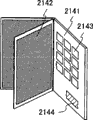
In addition, Figure 14 E illustrates e-book (being also referred to as Electronic Paper).This e-book comprises main body 2141, display part 2142, operation keys 2143, the semiconductor device of the present invention 2144 with function of storage device, MPU, imageing sensor etc.In addition, both can be in main body 2141 built-in modulator-demodulator, also can adopt the structure that can wirelessly receive and send messages.
Such as stated, the range of application of semiconductor device of the present invention is very extensive, can be used in other electronic equipments.
Claims (16)
1. the manufacturing approach of a semiconductor device is characterized in that, comprises the steps:
First corpus fibrosum is set on the first surface of device substrate, and this device substrate has active element;
Be coated with first composition that comprises first organic resin from said first corpus fibrosum and said device substrate top, said first corpus fibrosum is flooded by said first organic resin; And
After said first composition of coating, through said device substrate is heated, form first sealant that comprises said first corpus fibrosum and said first organic resin,
Second corpus fibrosum is set on the second surface of said device substrate, and the first surface of this second surface and said device substrate is opposite;
Said second corpus fibrosum and said device substrate are coated with second composition that comprises second organic resin, said second corpus fibrosum is flooded by said second organic resin;
After said second composition of coating, through said device substrate is heated, form second sealant that comprises said second corpus fibrosum and said second organic resin,
The warp thread of the warp thread of wherein said first corpus fibrosum or the direction of weft yarn and second corpus fibrosum or the direction of weft yarn differ 30 °~60 °,
And the thickness of said sealant is more than or equal to 10 microns and be less than or equal to 100 microns.
2. the manufacturing approach of semiconductor device as claimed in claim 1 is characterized in that, also comprises the steps: to form the insulating barrier that covers said active element.
3. the manufacturing approach of semiconductor device as claimed in claim 1 is characterized in that, also comprises the steps: on said device substrate, to form antenna.
4. the manufacturing approach of semiconductor device as claimed in claim 1 is characterized in that, said device substrate uses the SOI substrate to form.
5. the manufacturing approach of semiconductor device as claimed in claim 1 is characterized in that, said active element is one or more in MOS transistor, non-volatile memory device and the diode.
6. the manufacturing approach of semiconductor device as claimed in claim 1 is characterized in that, said first corpus fibrosum and second corpus fibrosum comprise glass fiber.
7. the manufacturing approach of a semiconductor device is characterized in that, comprises the steps:
On the first surface of device substrate, form first organic resin layer, this device substrate has active element;
On said first organic resin layer and said device substrate, first corpus fibrosum is set, said first corpus fibrosum is flooded by first organic resin of first organic resin layer; And
After said first corpus fibrosum is set, through said device substrate is heated, form first sealant that comprises said first corpus fibrosum and said first organic resin,
On the second surface of said device substrate, form second organic resin layer, the first surface of this second surface and said device substrate is opposite;
On said second organic resin layer and said device substrate, second corpus fibrosum is set, said second corpus fibrosum is flooded by second organic resin of said second organic resin layer;
After said second corpus fibrosum is set, through said device substrate is heated, form second sealant that comprises said second corpus fibrosum and said second organic resin,
And the warp thread of the warp thread of said first corpus fibrosum or the direction of weft yarn and second corpus fibrosum or the direction of weft yarn differ 30 °~60 °, and the thickness of said sealant is more than or equal to 10 microns and be less than or equal to 100 microns.
8. the manufacturing approach of semiconductor device as claimed in claim 7 is characterized in that, also comprises the steps: to form the insulating barrier that covers said active element.
9. the manufacturing approach of semiconductor device as claimed in claim 7 is characterized in that, also comprises the steps: on said device substrate, to form antenna.
10. the manufacturing approach of semiconductor device as claimed in claim 7 is characterized in that, said device substrate uses the SOI substrate to form.
11. the manufacturing approach of semiconductor device as claimed in claim 7 is characterized in that, said active element is one or more in MOS transistor, non-volatile memory device and the diode.
12. the manufacturing approach of semiconductor device as claimed in claim 7 is characterized in that, said first corpus fibrosum and second corpus fibrosum comprise glass fiber.
13. the manufacturing approach of a semiconductor device is characterized in that, comprises the steps:
First corpus fibrosum is set on the first surface of device substrate, and this device substrate has the active element and first distribution;
Be coated with first composition that comprises first organic resin from said first corpus fibrosum and said device substrate top, said first corpus fibrosum is flooded by said first organic resin;
After said first composition of coating,, form first sealant that comprises said first corpus fibrosum and said first organic resin through said device substrate is heated;
In first peristome of said first sealant, form first splicing ear that is connected to said first distribution; And
First base plate bonding that will have first antenna is electrically connected to each other said first splicing ear and said first antenna to said first sealant,
Second corpus fibrosum is set on the second surface of said device substrate, and the first surface of this second surface and said device substrate is opposite;
Said second corpus fibrosum and said device substrate are coated with second composition that comprises second organic resin, said second corpus fibrosum is flooded by said second organic resin;
After said second composition of coating, through said device substrate is heated, form second sealant that comprises said second corpus fibrosum and said second organic resin,
The warp thread of the warp thread of wherein said first corpus fibrosum or the direction of weft yarn and second corpus fibrosum or the direction of weft yarn differ 30 °~60 °,
And the thickness of said sealant is more than or equal to 10 microns and be less than or equal to 100 microns.
14. the manufacturing approach of semiconductor device as claimed in claim 13 is characterized in that, also comprises the steps:
Form second peristome, a part that is formed on second distribution in the said device substrate is exposed;
In said second peristome of said second sealant, form second splicing ear that is connected to said second distribution; And
Second base plate bonding that will have second antenna is electrically connected to each other said second splicing ear and said second antenna to said second sealant.
15. the manufacturing approach of a semiconductor device is characterized in that, comprises the steps:
On the first surface of device substrate, form first organic resin layer, this device substrate has the active element and first distribution;
On said first organic resin layer and said device substrate, first corpus fibrosum is set, said first corpus fibrosum is flooded by first organic resin of said first organic resin layer;
After said first corpus fibrosum is set,, form first sealant that comprises said first corpus fibrosum and said first organic resin through said device substrate is heated;
In first peristome of said first organic resin layer, form first splicing ear that is connected to said first distribution; And
First base plate bonding that will have first antenna is electrically connected to each other said first splicing ear and said first antenna to said first sealant,
On the second surface of said device substrate, form second organic resin layer;
On said second organic resin layer and said device substrate, second corpus fibrosum is set, said second corpus fibrosum is flooded by second organic resin of said second organic resin layer;
After said second corpus fibrosum is set; Through said device substrate is heated; Formation comprises second sealant of said second corpus fibrosum and said second organic resin; The warp thread of the warp thread of wherein said first corpus fibrosum or the direction of weft yarn and second corpus fibrosum or the direction of weft yarn differ 30 °~60 °
And the thickness of said sealant is more than or equal to 10 microns and be less than or equal to 100 microns.
16. the manufacturing approach of semiconductor device as claimed in claim 15 is characterized in that, also comprises the steps:
Form second peristome, a part that is formed on second distribution in the said device substrate is exposed;
In said second peristome of said second organic resin layer, form second splicing ear that is connected to said second distribution; And
Second base plate bonding that will have second antenna is electrically connected to each other said second splicing ear and said second antenna to said second sealant.
Applications Claiming Priority (2)
| Application Number | Priority Date | Filing Date | Title |
|---|---|---|---|
| JP2007079264 | 2007-03-26 | ||
| JP2007-079264 | 2007-03-26 |
Publications (2)
| Publication Number | Publication Date |
|---|---|
| CN101276767A CN101276767A (en) | 2008-10-01 |
| CN101276767B true CN101276767B (en) | 2012-12-12 |
Family
ID=39643903
Family Applications (1)
| Application Number | Title | Priority Date | Filing Date |
|---|---|---|---|
| CN2008100879672A Expired - Fee Related CN101276767B (en) | 2007-03-26 | 2008-03-25 | Method for manufacturing semiconductor device |
Country Status (6)
| Country | Link |
|---|---|
| US (1) | US7785933B2 (en) |
| EP (1) | EP1976000A3 (en) |
| JP (1) | JP2008270762A (en) |
| KR (1) | KR101466594B1 (en) |
| CN (1) | CN101276767B (en) |
| TW (1) | TWI442513B (en) |
Families Citing this family (33)
| Publication number | Priority date | Publication date | Assignee | Title |
|---|---|---|---|---|
| KR101478810B1 (en) | 2006-07-28 | 2015-01-02 | 가부시키가이샤 한도오따이 에네루기 켄큐쇼 | Power storage device |
| EP1970951A3 (en) * | 2007-03-13 | 2009-05-06 | Semiconductor Energy Laboratory Co., Ltd. | Semiconductor device and manufacturing method thereof |
| EP1970952A3 (en) | 2007-03-13 | 2009-05-06 | Semiconductor Energy Laboratory Co., Ltd. | Semiconductor device and manufacturing method thereof |
| JP5268395B2 (en) * | 2007-03-26 | 2013-08-21 | 株式会社半導体エネルギー研究所 | Method for manufacturing semiconductor device |
| JP2009205669A (en) * | 2008-01-31 | 2009-09-10 | Semiconductor Energy Lab Co Ltd | Semiconductor device |
| JP5473413B2 (en) * | 2008-06-20 | 2014-04-16 | 株式会社半導体エネルギー研究所 | Wiring substrate manufacturing method, antenna manufacturing method, and semiconductor device manufacturing method |
| JP2010041045A (en) * | 2008-07-09 | 2010-02-18 | Semiconductor Energy Lab Co Ltd | Semiconductor device and method for producing the same |
| JP2010041040A (en) * | 2008-07-10 | 2010-02-18 | Semiconductor Energy Lab Co Ltd | Photoelectric conversion device and method of manufacturing the same |
| JP5358324B2 (en) * | 2008-07-10 | 2013-12-04 | 株式会社半導体エネルギー研究所 | Electronic paper |
| KR101753574B1 (en) * | 2008-07-10 | 2017-07-04 | 가부시키가이샤 한도오따이 에네루기 켄큐쇼 | Light emitting device and electronic device |
| WO2010035627A1 (en) | 2008-09-25 | 2010-04-01 | Semiconductor Energy Laboratory Co., Ltd. | Semiconductor device |
| JP5583951B2 (en) * | 2008-11-11 | 2014-09-03 | 株式会社半導体エネルギー研究所 | Method for manufacturing semiconductor device |
| JP5470054B2 (en) | 2009-01-22 | 2014-04-16 | 株式会社半導体エネルギー研究所 | Semiconductor device |
| GB2469628A (en) * | 2009-04-20 | 2010-10-27 | Michael Edward Beese | Two Part Identification Label |
| WO2010140539A1 (en) * | 2009-06-05 | 2010-12-09 | Semiconductor Energy Laboratory Co., Ltd. | Photoelectric conversion device and method for manufacturing the same |
| KR101732397B1 (en) * | 2009-06-05 | 2017-05-04 | 가부시키가이샤 한도오따이 에네루기 켄큐쇼 | Photoelectric conversion device and manufacturing method thereof |
| WO2010140495A1 (en) * | 2009-06-05 | 2010-12-09 | Semiconductor Energy Laboratory Co., Ltd. | Photoelectric conversion device and method for manufacturing the same |
| US8345435B2 (en) * | 2009-08-07 | 2013-01-01 | Semiconductor Energy Laboratory Co., Ltd. | Terminal structure and manufacturing method thereof, and electronic device and manufacturing method thereof |
| JP5719560B2 (en) * | 2009-10-21 | 2015-05-20 | 株式会社半導体エネルギー研究所 | Manufacturing method of terminal structure |
| JP5896594B2 (en) * | 2010-05-14 | 2016-03-30 | 株式会社村田製作所 | Wireless IC device |
| CN102403225B (en) * | 2010-09-07 | 2013-08-14 | 无锡华润上华半导体有限公司 | Manufacturing method and device of channel double-diffusion metal oxide semiconductor |
| US8518798B2 (en) * | 2010-09-23 | 2013-08-27 | Infineon Technologies Ag | Semiconductor structure and method for making same |
| KR101679657B1 (en) | 2010-09-29 | 2016-11-25 | 삼성전자주식회사 | Method for wafer level mold and wafer structure formed by the same |
| WO2012070035A1 (en) * | 2010-11-26 | 2012-05-31 | The National Microelectronics Applications Centre Limited | An ac current or voltage sensor |
| US20130229776A1 (en) * | 2011-12-23 | 2013-09-05 | Wisconsin Alumni Research Foundation | High-speed, flexible integrated circuits and methods for making high-speed, flexible integrated circuits |
| JP2014135422A (en) * | 2013-01-11 | 2014-07-24 | Toyota Motor Corp | Semiconductor device manufacturing method |
| KR102086098B1 (en) * | 2013-07-03 | 2020-03-09 | 삼성디스플레이 주식회사 | Display device |
| KR102135275B1 (en) * | 2013-07-29 | 2020-07-20 | 삼성디스플레이 주식회사 | Thin film transistor substrate, method of manufacturing the same and display device comprising the same |
| KR101418974B1 (en) * | 2014-01-23 | 2014-07-14 | 김용석 | Protective film management system for smart phone |
| KR101821861B1 (en) | 2015-10-15 | 2018-01-25 | 한국과학기술원 | Wearable memory with textile substrate and manufacturing method thereof |
| US20170170016A1 (en) * | 2015-12-14 | 2017-06-15 | Globalfoundries Inc. | Multiple patterning method for substrate |
| DE102016107678B4 (en) * | 2016-04-26 | 2023-12-28 | Infineon Technologies Ag | SEMICONDUCTOR DEVICES WITH ON-CHIP ANTENNAS AND THEIR PRODUCTION |
| JP6577910B2 (en) * | 2016-06-23 | 2019-09-18 | ルネサスエレクトロニクス株式会社 | Electronic equipment |
Citations (1)
| Publication number | Priority date | Publication date | Assignee | Title |
|---|---|---|---|---|
| CN85104878A (en) * | 1985-05-26 | 1987-01-07 | 米尔顿·伊万·罗斯 | The encapsulation of electronic circuit device and manufacture method thereof and equipment |
Family Cites Families (49)
| Publication number | Priority date | Publication date | Assignee | Title |
|---|---|---|---|---|
| CA2026113C (en) | 1989-01-25 | 1998-12-01 | Tsunoe Igarashi | Prepreg, composite molded body, and method of manufacture of the composite molded body |
| DE3907757A1 (en) | 1989-03-10 | 1990-09-13 | Mtu Muenchen Gmbh | PROTECTIVE FILM |
| JPH04196346A (en) * | 1990-11-28 | 1992-07-16 | Hitachi Ltd | Thin resin-sealed semiconductor device |
| US5888609A (en) | 1990-12-18 | 1999-03-30 | Valtion Teknillinen Tutkimuskeskus | Planar porous composite structure and method for its manufacture |
| JPH05190582A (en) | 1992-01-08 | 1993-07-30 | Oki Electric Ind Co Ltd | Resin sealed semiconductor device and manufacture thereof |
| JP3578466B2 (en) * | 1992-04-14 | 2004-10-20 | ユニチカ株式会社 | Inorganic fiber woven fabric for reinforcement and multilayer printed wiring board using the same |
| JPH077246A (en) * | 1993-06-17 | 1995-01-10 | Kobe Steel Ltd | Manufacture of in-molded product containing electronic component constituting material |
| WO1995033246A1 (en) | 1994-05-27 | 1995-12-07 | Ake Gustafson | Method for fabricating an electronic module and electronic module obtained thereby |
| TW371285B (en) * | 1994-09-19 | 1999-10-01 | Amp Akzo Linlam Vof | Foiled UD-prepreg and PWB laminate prepared therefrom |
| JP3364081B2 (en) | 1995-02-16 | 2003-01-08 | 株式会社半導体エネルギー研究所 | Method for manufacturing semiconductor device |
| US5757456A (en) | 1995-03-10 | 1998-05-26 | Semiconductor Energy Laboratory Co., Ltd. | Display device and method of fabricating involving peeling circuits from one substrate and mounting on other |
| JP4015717B2 (en) * | 1995-06-29 | 2007-11-28 | 日立マクセル株式会社 | Information carrier manufacturing method |
| JPH09116182A (en) * | 1995-10-17 | 1997-05-02 | Canon Inc | Solar battery module and manufacture of solar battery module |
| US6482495B1 (en) | 1996-09-04 | 2002-11-19 | Hitachi Maxwell, Ltd. | Information carrier and process for production thereof |
| JPH1092980A (en) * | 1996-09-13 | 1998-04-10 | Toshiba Corp | Wireless card and production thereof |
| JP3428472B2 (en) * | 1998-12-03 | 2003-07-22 | 富士通株式会社 | Printed board unit and method of manufacturing the printed board unit |
| JP2004078991A (en) | 1998-12-17 | 2004-03-11 | Hitachi Ltd | Semiconductor device and its manufacturing method |
| TW484101B (en) | 1998-12-17 | 2002-04-21 | Hitachi Ltd | Semiconductor device and its manufacturing method |
| US6224965B1 (en) | 1999-06-25 | 2001-05-01 | Honeywell International Inc. | Microfiber dielectrics which facilitate laser via drilling |
| JP4423779B2 (en) * | 1999-10-13 | 2010-03-03 | 味の素株式会社 | Epoxy resin composition, adhesive film and prepreg using the composition, multilayer printed wiring board using the same, and method for producing the same |
| JP3675688B2 (en) | 2000-01-27 | 2005-07-27 | 寛治 大塚 | Wiring board and manufacturing method thereof |
| JP4884592B2 (en) | 2000-03-15 | 2012-02-29 | 株式会社半導体エネルギー研究所 | Method for manufacturing light emitting device and method for manufacturing display device |
| JP4703030B2 (en) * | 2001-05-15 | 2011-06-15 | 旭化成イーマテリアルズ株式会社 | Glass cloth patterned by plating |
| US8415208B2 (en) | 2001-07-16 | 2013-04-09 | Semiconductor Energy Laboratory Co., Ltd. | Semiconductor device and peeling off method and method of manufacturing semiconductor device |
| JP2003049388A (en) | 2001-08-08 | 2003-02-21 | Du Pont Toray Co Ltd | Fabric comprising flat aramid fiber |
| US6903377B2 (en) | 2001-11-09 | 2005-06-07 | Semiconductor Energy Laboratory Co., Ltd. | Light emitting apparatus and method for manufacturing the same |
| KR100430001B1 (en) | 2001-12-18 | 2004-05-03 | 엘지전자 주식회사 | Manufacturing method of multi-layer pcb, pad fabricating method of multi-layer pcb, semiconductor pkg manufacturing method using multi-layer pcb |
| JP2003282610A (en) * | 2002-01-16 | 2003-10-03 | Nippon Koden Corp | Insulating method of conductive part and manufacturing method of semiconductor sensor |
| US7485489B2 (en) | 2002-06-19 | 2009-02-03 | Bjoersell Sten | Electronics circuit manufacture |
| EP1514307A1 (en) | 2002-06-19 | 2005-03-16 | Sten Bjorsell | Electronics circuit manufacture |
| JP2004140267A (en) | 2002-10-18 | 2004-05-13 | Semiconductor Energy Lab Co Ltd | Semiconductor device and fabrication method thereof |
| JP4828088B2 (en) | 2003-06-05 | 2011-11-30 | 凸版印刷株式会社 | IC tag |
| JP4540359B2 (en) | 2004-02-10 | 2010-09-08 | シャープ株式会社 | Semiconductor device and manufacturing method thereof |
| US20050233122A1 (en) | 2004-04-19 | 2005-10-20 | Mikio Nishimura | Manufacturing method of laminated substrate, and manufacturing apparatus of semiconductor device for module and laminated substrate for use therein |
| EP1774595A4 (en) | 2004-06-02 | 2011-05-18 | Semiconductor Energy Lab | Laminating system |
| KR20060045208A (en) * | 2004-11-12 | 2006-05-17 | 삼성테크윈 주식회사 | Printed circuit for semi-conductor package and method for manufacturing the same |
| US7736964B2 (en) | 2004-11-22 | 2010-06-15 | Semiconductor Energy Laboratory Co., Ltd. | Semiconductor device, and method for manufacturing the same |
| US7465674B2 (en) | 2005-05-31 | 2008-12-16 | Semiconductor Energy Laboratory Co., Ltd. | Manufacturing method of semiconductor device |
| US7727859B2 (en) | 2005-06-30 | 2010-06-01 | Semiconductor Energy Laboratory Co., Ltd | Semiconductor device and manufacturing method thereof |
| US7685706B2 (en) * | 2005-07-08 | 2010-03-30 | Semiconductor Energy Laboratory Co., Ltd | Method of manufacturing a semiconductor device |
| JP5127178B2 (en) * | 2005-07-29 | 2013-01-23 | 株式会社半導体エネルギー研究所 | Method for manufacturing semiconductor device |
| US7700463B2 (en) | 2005-09-02 | 2010-04-20 | Semiconductor Energy Laboratory Co., Ltd. | Method for manufacturing semiconductor device |
| JP4682764B2 (en) | 2005-09-15 | 2011-05-11 | 日立化成デュポンマイクロシステムズ株式会社 | Positive photosensitive resin composition, pattern forming method, and electronic component |
| JP2007091822A (en) | 2005-09-27 | 2007-04-12 | Shin Kobe Electric Mach Co Ltd | Prepreg |
| TWI431726B (en) | 2006-06-01 | 2014-03-21 | Semiconductor Energy Lab | Nonvolatile semiconductor memory device |
| WO2008001703A1 (en) | 2006-06-26 | 2008-01-03 | Semiconductor Energy Laboratory Co., Ltd. | Paper including semiconductor device and manufacturing method thereof |
| EP1970951A3 (en) * | 2007-03-13 | 2009-05-06 | Semiconductor Energy Laboratory Co., Ltd. | Semiconductor device and manufacturing method thereof |
| EP1970952A3 (en) * | 2007-03-13 | 2009-05-06 | Semiconductor Energy Laboratory Co., Ltd. | Semiconductor device and manufacturing method thereof |
| JP5268395B2 (en) * | 2007-03-26 | 2013-08-21 | 株式会社半導体エネルギー研究所 | Method for manufacturing semiconductor device |
-
2008
- 2008-03-11 EP EP08004496A patent/EP1976000A3/en not_active Withdrawn
- 2008-03-12 JP JP2008062132A patent/JP2008270762A/en not_active Withdrawn
- 2008-03-14 US US12/076,148 patent/US7785933B2/en not_active Expired - Fee Related
- 2008-03-24 KR KR1020080027015A patent/KR101466594B1/en active IP Right Grant
- 2008-03-24 TW TW097110380A patent/TWI442513B/en not_active IP Right Cessation
- 2008-03-25 CN CN2008100879672A patent/CN101276767B/en not_active Expired - Fee Related
Patent Citations (1)
| Publication number | Priority date | Publication date | Assignee | Title |
|---|---|---|---|---|
| CN85104878A (en) * | 1985-05-26 | 1987-01-07 | 米尔顿·伊万·罗斯 | The encapsulation of electronic circuit device and manufacture method thereof and equipment |
Non-Patent Citations (2)
| Title |
|---|
| JP特开平10-92980A 1998.04.10 |
| JP特开平7-7246A 1995.01.10 |
Also Published As
| Publication number | Publication date |
|---|---|
| TW200903720A (en) | 2009-01-16 |
| JP2008270762A (en) | 2008-11-06 |
| CN101276767A (en) | 2008-10-01 |
| KR101466594B1 (en) | 2014-11-28 |
| EP1976000A2 (en) | 2008-10-01 |
| US20080311706A1 (en) | 2008-12-18 |
| US7785933B2 (en) | 2010-08-31 |
| KR20080087693A (en) | 2008-10-01 |
| TWI442513B (en) | 2014-06-21 |
| EP1976000A3 (en) | 2009-05-13 |
Similar Documents
| Publication | Publication Date | Title |
|---|---|---|
| CN101276767B (en) | Method for manufacturing semiconductor device | |
| CN101276743B (en) | Method for manufacturing semiconductor device | |
| CN101266954B (en) | Semiconductor device and manufacturing method thereof | |
| CN101266953B (en) | Semiconductor device and manufacturing method thereof | |
| CN101803008B (en) | Semiconductor device and method for manufacturing the same | |
| JP5298216B2 (en) | Semiconductor device | |
| JP5004537B2 (en) | Semiconductor device | |
| JP5352048B2 (en) | Method for manufacturing semiconductor device |
Legal Events
| Date | Code | Title | Description |
|---|---|---|---|
| C06 | Publication | ||
| PB01 | Publication | ||
| C10 | Entry into substantive examination | ||
| SE01 | Entry into force of request for substantive examination | ||
| C14 | Grant of patent or utility model | ||
| GR01 | Patent grant | ||
| CF01 | Termination of patent right due to non-payment of annual fee | ||
| CF01 | Termination of patent right due to non-payment of annual fee |
Granted publication date: 20121212 Termination date: 20200325 |