JP2008004280A - Flat panel display device - Google Patents
Flat panel display device Download PDFInfo
- Publication number
- JP2008004280A JP2008004280A JP2006169986A JP2006169986A JP2008004280A JP 2008004280 A JP2008004280 A JP 2008004280A JP 2006169986 A JP2006169986 A JP 2006169986A JP 2006169986 A JP2006169986 A JP 2006169986A JP 2008004280 A JP2008004280 A JP 2008004280A
- Authority
- JP
- Japan
- Prior art keywords
- anode
- anode electrode
- electrode
- display device
- panel
- Prior art date
- Legal status (The legal status is an assumption and is not a legal conclusion. Google has not performed a legal analysis and makes no representation as to the accuracy of the status listed.)
- Pending
Links
Images


Abstract
Description
本発明は、平面型表示装置に関する。 The present invention relates to a flat display device.
現在主流の陰極線管(CRT)に代わる画像表示装置として、平面型(フラットパネル形式)の表示装置が種々検討されている。このような平面型の表示装置として、液晶表示装置(LCD)、エレクトロルミネッセンス表示装置(ELD)、プラズマ表示装置(PDP)を例示することができる。また、電子放出素子を備えたカソードパネルを組み込んだ平面型表示装置の開発も進められている。ここで、電子放出素子として、冷陰極電界電子放出素子、金属/絶縁膜/金属型素子(MIM素子とも呼ばれる)、表面伝導型電子放出素子が知られており、これらの冷陰極電子源から構成された電子放出素子を備えたカソードパネルを組み込んだ平面型表示装置は、高解像度、高輝度のカラー表示、及び、低消費電力の観点から注目を集めている。 As an image display device that can replace the mainstream cathode ray tube (CRT), various types of flat display devices have been studied. Examples of such a flat display device include a liquid crystal display device (LCD), an electroluminescence display device (ELD), and a plasma display device (PDP). In addition, development of a flat display device incorporating a cathode panel equipped with an electron-emitting device is also in progress. Here, as the electron-emitting device, a cold cathode field electron-emitting device, a metal / insulating film / metal-type device (also called MIM device), and a surface conduction electron-emitting device are known. A flat display device incorporating a cathode panel provided with the electron-emitting device is attracting attention from the viewpoint of high-resolution, high-luminance color display and low power consumption.
冷陰極電界電子放出素子を組み込んだ平面型表示装置である冷陰極電界電子放出表示装置(以下、表示装置と略称する場合がある)は、一般に、2次元マトリックス状に配列された各サブピクセルに対応した電子放出領域を有するカソードパネルと、電子放出領域から放出された電子との衝突により励起されて発光する蛍光体領域を有するアノードパネルとが、真空に保持された空間を介して対向配置された構成を有する。電子放出領域には、通常、1又は複数の冷陰極電界電子放出素子(以下、電界放出素子と略称する場合がある)が設けられている。電界放出素子として、スピント型、扁平型、エッジ型、平面型等を挙げることができる。 In general, a cold cathode field emission display device (hereinafter sometimes abbreviated as a display device), which is a flat display device incorporating a cold cathode field emission device, has a sub-pixel arranged in a two-dimensional matrix. A cathode panel having a corresponding electron emission region and an anode panel having a phosphor region that emits light when excited by collision with electrons emitted from the electron emission region are arranged to face each other through a space held in a vacuum. Have a configuration. The electron emission region is usually provided with one or a plurality of cold cathode field emission devices (hereinafter sometimes abbreviated as field emission devices). Examples of field emission devices include Spindt type, flat type, edge type, and planar type.
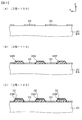
特開2004−158232号公報の発明の実施の形態2に開示された表示装置におけるアノード電極の模式的な平面図を図10に示し、図10の矢印A−A、矢印B−B及び矢印C−Cに沿ったアノードパネルAPの模式的な一部端面図を図11の(A)、(B)及び(C)に示す。また、この表示装置の模式的な一部端面図を図12に示し、アノードパネルAP及びカソードパネルCPの模式的な部分的斜視図を図13に示す。尚、図13においては、図面の簡素化のため、アノード電極ユニットとしての図示を省略しており、隔壁の図示も省略している。
FIG. 10 shows a schematic plan view of the anode electrode in the display device disclosed in
この表示装置は、複数の電子放出領域が設けられたカソードパネルCPと、蛍光体領域及びアノード電極が設けられたアノードパネルAPとが、それらの周縁部で接合されて成る。電子放出領域には複数の電界放出素子が設けられている。 In this display device, a cathode panel CP provided with a plurality of electron emission regions and an anode panel AP provided with a phosphor region and an anode electrode are joined at their peripheral portions. A plurality of field emission elements are provided in the electron emission region.
図12に示した電界放出素子は、円錐形の電子放出部を有する、所謂スピント(Spindt)型電界放出素子と呼ばれるタイプの電界放出素子である。この電界放出素子は、支持体10上に形成されたカソード電極11と、支持体10及びカソード電極11上に形成された絶縁層12と、絶縁層12上に形成されたゲート電極13と、ゲート電極13及び絶縁層12に設けられた開口部14(ゲート電極13に設けられた第1開口部14A、及び、絶縁層12に設けられた第2開口部14B)と、第2開口部14Bの底部に位置するカソード電極11上に形成された円錐形の電子放出部15から構成されている。一般に、カソード電極11とゲート電極13とは、これらの両電極11,13の射影像が互いに直交する方向に各々帯状に形成されている。帯状のカソード電極11と帯状のゲート電極13とが重複する重複領域が、電子放出領域EAであり、1サブピクセルの領域に相当する。そして、係る電子放出領域EAが、カソードパネルCPの有効領域(表示装置の表示領域に対応する領域)内に、通常、2次元マトリックス状に配列されている。
The field emission device shown in FIG. 12 is a so-called Spindt type field emission device having a conical electron emission portion. The field emission device includes a
一方、アノードパネルAPは、基板120と、基板120上に形成され、所定のパターンを有する単位蛍光体領域121と、その上に形成されたアノード電極130と、給電部140(図12には図示せず)から構成されている。アノード電極130は、全体として、矩形の有効領域を覆う形状を有し、アルミニウム薄膜から構成されている。アノード電極130は、単位蛍光体領域121からの発光を反射させる反射膜としての機能を有する。単位蛍光体領域121と単位蛍光体領域121との間の基板120上には光吸収層(ブラック・マトリックス)122が形成されている。また、光吸収層122の上には隔壁123が形成されている。隔壁123の平面形状は、格子形状(井桁形状)であり、1サブピクセル(単位蛍光体領域)を取り囲む形状を有する。
On the other hand, the anode panel AP is formed on the
ここで、1サブピクセルは、カソードパネル側のカソード電極11とゲート電極13との重複領域に設けられた電界放出素子の一群と、これらの電界放出素子の一群に対面したアノードパネル側の単位蛍光体領域121(1つの赤色発光単位蛍光体領域、1つの緑色発光単位蛍光体領域、あるいは、1つの青色発光単位蛍光体領域)とによって構成されている。表示領域には、かかるサブピクセルが、例えば数十万〜数百万個ものオーダーにて配列されている。また、1画素(1ピクセル)は3つのサブピクセルから構成されている。
Here, one subpixel is a group of field emission elements provided in an overlapping region of the
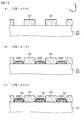
アノード電極130は、単位蛍光体領域121を覆うアノード電極ユニット131の集合体から構成されている。アノード電極ユニット131の間には、ギャップ132A,132Bが設けられている。尚、ギャップ132Aは単位蛍光体領域121が形成されていない基板120の部分に設けられており、ギャップ132Bは隔壁123の頂面上に位置するように、あるいは又、隔壁123を跨って形成されている。アノード電極ユニット131とアノード電極ユニット131との間には抵抗体層133が形成されている。より具体的には、抵抗体層133は、ギャップ132A,132Bを越え、隣接するアノード電極ユニット131間を跨るように形成されている。抵抗体層133は、例えばシリコンカーバイド(SiC)から成る抵抗体薄膜から構成され、スパッタリング法にて形成されている。
The
アノード電極ユニット131の大きさは、アノード電極ユニット131と電界放出素子(より具体的には、ゲート電極13あるいはカソード電極11)との間で生じた放電により発生したエネルギーによってアノード電極ユニット131が局所的に蒸発しない大きさ(より具体的には、アノード電極ユニット131とゲート電極13あるいはカソード電極11との間で生じた放電により発生したエネルギーによって、アノード電極ユニット131において1サブピクセルに相当する大きさの部分が蒸発しない大きさ)である。尚、図10においては、図面を簡素化するために、4×4のアノード電極ユニット131を図示し、模式的な一部断面図においては、1つのアノード電極ユニット131が複数の単位蛍光体領域を覆うが如くに図示しているが、実際には、アノード電極ユニット131の大きさは、例えば、単位蛍光体領域を被覆する大きさ、即ち、1サブピクセルに相当する大きさである。
The size of the
そして、アノード電極130の一辺を構成するアノード電極ユニット131Aは、給電部140を介してアノード電極制御回路53に接続されている。アノード電極制御回路53と給電部140との間には、通常、過電流や放電を防止するための抵抗体R0が配設されている。ここで、給電部140は、給電部抵抗体層143を介して直列に接続された給電部ユニット141から構成されている。そして、給電部ユニット141と給電部ユニット141との間には隙間142Aが設けられ、給電部ユニット141と給電部ユニット141との間を跨るように、隙間142Aの上に給電部抵抗体層143が形成されている。給電部ユニット141も、例えばアルミニウム薄膜から構成されている。そして、アノード電極130の一辺を構成するアノード電極ユニット131Aと給電部ユニット141との間には隙間142Bが設けられており、アノード電極130の一辺を構成するアノード電極ユニット131Aと給電部ユニット141とは、抵抗部材134を介して接続されている。抵抗部材134は、アノード電極ユニット131と給電部ユニット141との間を跨るように、化学的気相成長法(CVD法)に基づき、隙間142Bの上に形成されている。
The
そして、特開2004−158232号公報に開示された表示装置にあっては、アノード電極を有効領域のほぼ全面に亙って形成する代わりに、より小さい面積を有するアノード電極ユニット131に分割した形で形成するので、アノード電極ユニット131と冷陰極電界電子放出素子との間の静電容量を小さくすることができる。その結果、放電の発生を低減することができ、放電に起因したアノード電極や冷陰極電界電子放出素子の損傷の発生を効果的に減少させることができる。
In the display device disclosed in Japanese Patent Laid-Open No. 2004-158232, the anode electrode is divided into
このように、特開2004−158232号公報に開示された表示装置にあっては、放電の発生を減少させることができる。しかし、アノード電極ユニット等を形成するために導電材料層等をパターニングする複雑な工程が必要である。また、導電材料層等をパターニングする際には微小な異物の発生は避け難い。一般に、表示装置内の微小な異物は予期せぬ放電のトリガーとなる。アノード電極ユニット等を形成するためのパターニングにより生じた異物の除去が不充分であると、異物に起因する予期せぬ放電が増加してしまう。 Thus, in the display device disclosed in Japanese Patent Application Laid-Open No. 2004-158232, the occurrence of discharge can be reduced. However, in order to form an anode electrode unit or the like, a complicated process for patterning a conductive material layer or the like is required. In addition, when patterning the conductive material layer or the like, it is difficult to avoid generation of minute foreign matters. Generally, a minute foreign substance in the display device triggers an unexpected discharge. Insufficient removal of foreign matter caused by patterning to form an anode electrode unit or the like will increase unexpected discharge caused by the foreign matter.
従って、本発明の目的は、アノード電極ユニット等の形成を必要とすることなく、放電に起因したアノード電極や冷陰極電界電子放出素子の損傷の発生を効果的に減少させることができる平面型表示装置を提供することにある。 Accordingly, an object of the present invention is to provide a flat display capable of effectively reducing the occurrence of damage to the anode electrode and cold cathode field emission device due to discharge without the need for forming an anode electrode unit or the like. To provide an apparatus.
上記の目的を達成するための本発明の平面型表示装置は、
複数の電子放出領域が設けられたカソードパネルと、蛍光体領域及びアノード電極が設けられたアノードパネルとが、それらの周縁部で接合されて成る平面型表示装置であって、
アノードパネルは、
(a)基板、
(b)基板の表示領域上に形成された蛍光体領域、
(c)蛍光体領域上に形成された光反射層、及び、
(d)光反射層上に形成された、表示領域を覆うアノード電極、
を備えており、
(A)光反射層は絶縁材料から成り、
(B)アノード電極は抵抗材料から成ることを特徴とする。
In order to achieve the above object, a flat display device of the present invention comprises:
A flat panel display device in which a cathode panel provided with a plurality of electron emission regions and an anode panel provided with a phosphor region and an anode electrode are joined at the peripheral edge thereof.
The anode panel
(A) substrate,
(B) a phosphor region formed on the display region of the substrate;
(C) a light reflecting layer formed on the phosphor region, and
(D) an anode electrode formed on the light reflecting layer and covering the display area;
With
(A) The light reflecting layer is made of an insulating material,
(B) The anode electrode is made of a resistive material.
本発明の平面型表示装置にあっては、絶縁材料から成る光反射層が蛍光体領域上に形成されており、抵抗材料から成るアノード電極が、表示領域を覆い、光反射層上に形成されている。アノード電極と冷陰極電界電子放出素子との間にトリガーとなる放電が生ずると、アノードパネル内面(アノード電極)とカソードパネル内面(例えばゲート電極)との間に形成される静電容量に蓄えられた静電エネルギーは、電流として放電箇所を通じて流れ、放電を成長させようとする。即ち、アノード電極に蓄えられた静電エネルギーは、放電電流としてアノード電極を伝わって(アノード電極を流れて)、放電箇所に向かって流れこもうとする。本発明によれば、アノード電極と光反射層とはそれぞれ抵抗材料と絶縁材料とから成るので、アノード電極を流れる放電電流の大きさが抑制される。これにより、放電の成長ひいては放電により発生するエネルギーが抑制され、放電に起因したアノード電極や冷陰極電界電子放出素子の損傷の発生が減少する。また、蛍光体領域で発光しカソードパネル側に向かう光の一部は、絶縁材料から成る光反射層によってアノードパネル側に戻る。これにより、反射膜としても機能する従来のアノード電極を用いた構成と同様に、表示装置の発光効率を向上させることができる。光反射層上に形成され、表示領域を覆うアノード電極によって、光反射層はアノードパネルに確実に保持される。また、アノード電極を構成する抵抗材料の光吸収率にもよるが、アノード電極によって光反射層からカソードパネル側に向かう光の少なくとも一部は遮光される。これにより、カソードパネル側への不要な光漏れに起因する表示画像のコントラスト劣化が抑制される。 In the flat display device of the present invention, the light reflection layer made of an insulating material is formed on the phosphor region, and the anode electrode made of a resistance material covers the display region and is formed on the light reflection layer. ing. When a trigger discharge occurs between the anode electrode and the cold cathode field emission device, the discharge is stored in the capacitance formed between the inner surface of the anode panel (anode electrode) and the inner surface of the cathode panel (for example, the gate electrode). The electrostatic energy flows as a current through the discharge site and tries to grow the discharge. That is, the electrostatic energy stored in the anode electrode is transmitted as a discharge current through the anode electrode (flows through the anode electrode) and tends to flow toward the discharge location. According to the present invention, since the anode electrode and the light reflection layer are each made of a resistance material and an insulating material, the magnitude of the discharge current flowing through the anode electrode is suppressed. This suppresses the growth of the discharge and hence the energy generated by the discharge, and reduces the occurrence of damage to the anode electrode and the cold cathode field emission device due to the discharge. A part of the light emitted from the phosphor region and traveling toward the cathode panel is returned to the anode panel by the light reflecting layer made of an insulating material. Thereby, the light emission efficiency of the display device can be improved in the same manner as the configuration using the conventional anode electrode that also functions as a reflective film. The light reflection layer is securely held on the anode panel by the anode electrode formed on the light reflection layer and covering the display area. Further, although depending on the light absorption rate of the resistance material constituting the anode electrode, at least part of the light traveling from the light reflection layer toward the cathode panel is shielded by the anode electrode. Thereby, contrast deterioration of the display image due to unnecessary light leakage to the cathode panel side is suppressed.
本発明の平面型表示装置にあっては、通常の動作時において画像の輝度に応じたアノード電流が支障なくアノード電極を流れることが好ましい。従って、アノード電極のシート抵抗値は、平面型表示装置の通常の動作時におけるアノード電流の供給に支障がなく、かつ、アノード電極と冷陰極電界電子放出素子との間に放電が生じたとき、アノード電極を流れる放電電流の大きさを充分抑制し得る範囲にあることが望ましい。アノード電極のシート抵抗値として、1×10⁴Ω/□乃至2×105Ω/□、好ましくは2×104Ω/□乃至1×105Ω/□を例示することができる。 In the flat display device of the present invention, it is preferable that the anode current corresponding to the luminance of the image flows through the anode electrode without any trouble during normal operation. Accordingly, the sheet resistance value of the anode electrode has no hindrance to the supply of the anode current during the normal operation of the flat display device, and when a discharge occurs between the anode electrode and the cold cathode field emission device, It is desirable that the discharge current flowing through the anode electrode be in a range where the magnitude of the discharge current can be sufficiently suppressed. Examples of the sheet resistance value of the anode electrode include 1 × 10 4 Ω / □ to 2 × 10 5 Ω / □, preferably 2 × 10 4 Ω / □ to 1 × 10 5 Ω / □.
上記の好ましい形態、構成を含む本発明にあっては、蛍光体領域はマトリクス状に配置された複数の単位蛍光体領域から成り、隣り合う単位蛍光体領域の間の基板上には光吸収層が形成されており、アノード電極は光吸収層を覆うように形成されている構成とすることができる。この構成にあっては、光反射層は単位蛍光体領域上にのみ形成されていてもよいし、単位蛍光体領域上及び光吸収層上に形成されていてもよい。光吸収層は直接アノード電極により覆われていてもよいし、他の層(例えば、後述する隔壁)等を介して間接的に覆われていてもよい。光吸収層は基板上に平面的に形成されていてもよいし、立体的に形成されていてもよい。また、光吸収層の上に各単位蛍光体領域を取り囲む格子状の隔壁が設けられていてもよい。隔壁を設けることにより、単位蛍光体領域から反跳した電子、あるいは、単位蛍光体領域から放出された2次電子が他の単位蛍光体領域に入射し、所謂光学的クロストーク(色濁り)が発生することを防止することができる。光吸収層の上に隔壁が形成されており、アノード電極は隔壁を介して光吸収層を覆うように形成されている構成であってもよいし、光吸収層を覆うようにアノード電極が形成された後に、光吸収層に対応するアノード電極の部分の上に隔壁が形成されている構成であってもよい。 In the present invention including the above preferred embodiments and configurations, the phosphor region is composed of a plurality of unit phosphor regions arranged in a matrix, and a light absorption layer is formed on the substrate between adjacent unit phosphor regions. The anode electrode may be formed so as to cover the light absorption layer. In this configuration, the light reflection layer may be formed only on the unit phosphor region, or may be formed on the unit phosphor region and the light absorption layer. The light absorption layer may be directly covered with the anode electrode, or may be indirectly covered with another layer (for example, a partition wall described later) or the like. The light absorption layer may be planarly formed on the substrate or may be three-dimensionally formed. Further, a grid-like partition wall surrounding each unit phosphor region may be provided on the light absorption layer. By providing the partition walls, electrons recoiled from the unit phosphor region or secondary electrons emitted from the unit phosphor region enter another unit phosphor region, and so-called optical crosstalk (color turbidity) occurs. Occurrence can be prevented. A partition may be formed on the light absorption layer, and the anode electrode may be configured to cover the light absorption layer via the partition, or the anode electrode may be formed to cover the light absorption layer. Then, a structure in which a partition wall is formed on the portion of the anode electrode corresponding to the light absorption layer may be employed.
上記の好ましい形態、構成を含む本発明にあっては、抵抗材料から成るアノード電極にアノード電圧を印加する場合、例えばアノードパネルを構成する基板上に設けられ、導電材料から成る給電部を介して、アノード電圧を印加することができる。給電部の形状、給電部を構成する材料、給電部とアノード電極の形成の順序等は、平面型表示装置の設計に応じて適宜設定すればよい。基板上には表示領域を取り囲む給電部が設けられており、給電部とアノード電極とは積層されている構成とすることもできる。給電部は実質的に表示領域を取り囲む形状であればよく、必ずしも閉じた形状であることを要しない。この構成によれば、アノード電極の周囲に均一にアノード電圧が印加されるので、アノード電極全面における電位の均一性を良好なものとすることができる。給電部は、例えば、スピンコーティング法とリフトオフ法との組合せ、各種印刷法、リソグラフィ技術等、使用する材料に依存して適宜選択された方法にて形成することができる。給電部の構成材料として、モリブデン(Mo)、アルミニウム(Al)、クロム(Cr)、タングステン(W)等の金属材料、導電性粒子を含有するガラスペーストを例示することができる。 In the present invention including the above preferred form and configuration, when an anode voltage is applied to the anode electrode made of a resistance material, for example, it is provided on a substrate constituting the anode panel and is passed through a power feeding portion made of a conductive material. An anode voltage can be applied. What is necessary is just to set suitably the shape of a power supply part, the material which comprises a power supply part, the order of formation of a power supply part and an anode electrode, etc. according to the design of a flat type display apparatus. A power feeding unit surrounding the display area is provided on the substrate, and the power feeding unit and the anode electrode may be stacked. The power supply unit may be any shape that substantially surrounds the display area, and does not necessarily have to be a closed shape. According to this configuration, since the anode voltage is uniformly applied around the anode electrode, the potential uniformity over the entire anode electrode can be improved. The power feeding unit can be formed by a method appropriately selected depending on a material to be used, such as a combination of a spin coating method and a lift-off method, various printing methods, a lithography technique, and the like. Examples of the constituent material of the power feeding unit include metal materials such as molybdenum (Mo), aluminum (Al), chromium (Cr), and tungsten (W), and glass paste containing conductive particles.
以上に説明した好ましい形態、構成を含む本発明の平面型表示装置(以下、これらを総称して、単に、本発明と略称する場合がある)にあっては、光反射層を構成する絶縁材料として、真空条件下および加熱条件下で安定に存在する材料を広く用いることができる。例えば、絶縁性の化合物を用いて光反射層を形成することができる。光反射層が必要以上に厚くなると、蛍光体領域の帯電がアノード電極に流れにくくなる。従って、光反射層は光反射層の機能を確保しつつ、蛍光体領域の帯電がアノード電極に支障なく流れる程度のシート抵抗値を持つことが好ましい。形成された光反射層のシート抵抗値として、1×106Ω/□乃至1×1010Ω/□を例示することができる。光反射層を構成する絶縁性の化合物として、例えば、酸化チタン、酸化アルミニウム、酸化亜鉛、酸化マグネシウム等の金属酸化物;WSx等の金属硫化物;硫酸バリウム、炭酸カルシウム、リン酸カルシウム等の金属塩を挙げることができる。蛍光体領域(単位蛍光体領域)からの光を効果的に反射するために、平均粒径が約1×10-7m(約0.1μm)〜約4×10-7m(約0.4μm)の範囲、より好ましくは約1.5×10-7m(約0.15μm)〜約3×10-7m(約0.3μm)の範囲の絶縁材料の粒子によって白色の光反射層を構成することが望ましい。光反射層を塗布法等により形成する場合には、凝集を抑制するために、絶縁材料の粒子の表面に珪酸あるいはアルミナ等のコーティングが施されていてもよい。光反射層は、例えば、ポリビニルアルコール(PVA)樹脂と水に絶縁材料の粒子を分散させて、スピンコーティング法とリフトオフ法との組合せにより形成することができる。ポリビニルアルコール(PVA)樹脂の他、アクリル樹脂、アクリルエマルジョン等を用いても良い。光反射層は、各種印刷法、リソグラフィ技術等、使用する材料に依存して適宜選択された方法にて形成することができる。表示装置の発光効率の観点からは、光反射層の蛍光体領域側は滑らかな面に形成されていることが好ましい。例えば、蛍光体領域上に樹脂層を設け、光反射層を樹脂層上に形成し、その後、樹脂層を加熱処理等により除去することにより、光反射層の蛍光体領域側を滑らかな面に形成することができる。樹脂層を構成する材料として、ラッカーあるいはポリビニルアルコール(PVA)水溶液を挙げることができる。ここで、ラッカーには、広義のワニスの一種で、セルロース誘導体、一般にニトロセルロースを主成分とした配合物を低級脂肪酸エステルのような揮発性溶剤に溶かしたもの、あるいは、他の合成高分子を用いたウレタンラッカー、アクリルラッカー、クロム化合物やマンガン化合物が添加されたものが含まれる。ポリビニルアルコール水溶液の場合、希釈水溶液にグリコール系溶剤及びグリセリンを混合して乾燥速度を調整したもの、クロム化合物やマンガン化合物が添加されたものが含まれる。樹脂層の形成方法として、スクリーン印刷法;メタルマスク印刷法;ロールコーターやスプレーコーター、転写法を用いた塗布法;ラッカーフロート法(水槽に蓄えられた水中に基板を配した状態で水面に樹脂層を成膜し、水を抜くことで、樹脂層を基板上に付着させる方法)を例示することができる。加熱処理を施すことで樹脂層を除去するが、より具体的には、例えば、樹脂層が燃焼する温度での加熱処理を施すことで樹脂層を燃焼(分解除去)すればよい。 In the flat display device of the present invention including the preferred embodiments and configurations described above (hereinafter, these may be collectively referred to simply as the present invention), the insulating material constituting the light reflecting layer As such, materials that exist stably under vacuum conditions and heating conditions can be widely used. For example, the light reflecting layer can be formed using an insulating compound. If the light reflecting layer becomes thicker than necessary, the charging of the phosphor region becomes difficult to flow to the anode electrode. Therefore, it is preferable that the light reflection layer has a sheet resistance value that ensures the function of the light reflection layer and that the charging of the phosphor region flows without trouble to the anode electrode. Examples of the sheet resistance value of the formed light reflecting layer include 1 × 10 6 Ω / □ to 1 × 10 10 Ω / □. Examples of the insulating compound constituting the light reflecting layer include metal oxides such as titanium oxide, aluminum oxide, zinc oxide, and magnesium oxide; metal sulfides such as WS x ; metal salts such as barium sulfate, calcium carbonate, and calcium phosphate. Can be mentioned. In order to effectively reflect the light from the phosphor region (unit phosphor region), the average particle size is about 1 × 10 −7 m (about 0.1 μm) to about 4 × 10 −7 m (about 0.1 μm). 4 μm), more preferably white light reflecting layer by particles of insulating material in the range of about 1.5 × 10 −7 m (about 0.15 μm) to about 3 × 10 −7 m (about 0.3 μm) It is desirable to configure. When the light reflecting layer is formed by a coating method or the like, a coating such as silicic acid or alumina may be applied to the surface of the insulating material particles in order to suppress aggregation. The light reflecting layer can be formed by, for example, a combination of a spin coating method and a lift-off method in which particles of an insulating material are dispersed in polyvinyl alcohol (PVA) resin and water. In addition to the polyvinyl alcohol (PVA) resin, an acrylic resin, an acrylic emulsion, or the like may be used. The light reflecting layer can be formed by a method appropriately selected depending on the material to be used, such as various printing methods and lithography techniques. From the viewpoint of the luminous efficiency of the display device, the phosphor region side of the light reflecting layer is preferably formed on a smooth surface. For example, a resin layer is provided on the phosphor region, a light reflection layer is formed on the resin layer, and then the resin layer is removed by a heat treatment or the like, so that the phosphor region side of the light reflection layer is made smooth. Can be formed. Examples of the material constituting the resin layer include lacquer or polyvinyl alcohol (PVA) aqueous solution. Here, the lacquer is a kind of varnish in a broad sense, which is a cellulose derivative, generally a mixture of nitrocellulose as a main component dissolved in a volatile solvent such as a lower fatty acid ester, or other synthetic polymer. This includes urethane lacquers, acrylic lacquers, chromium compounds and manganese compounds used. In the case of an aqueous polyvinyl alcohol solution, a solution obtained by mixing a glycol solvent and glycerin in a dilute aqueous solution to adjust the drying speed, and a solution added with a chromium compound or a manganese compound are included. As a method for forming the resin layer, a screen printing method; a metal mask printing method; a coating method using a roll coater, a spray coater, or a transfer method; a lacquer float method (resin on the water surface with a substrate placed in water stored in a water tank) A method of depositing a resin layer on a substrate by forming a layer and draining water can be exemplified. The resin layer is removed by performing heat treatment. More specifically, for example, the resin layer may be burned (decomposed and removed) by performing heat treatment at a temperature at which the resin layer burns.
アノード電極を構成する抵抗材料として、真空条件下及び加熱条件下で安定に存在する材料を広く用いることができる。例えば、グラファイト(カーボン)等の半金属、酸化物、ホウ化物、炭化物、硫化物、及び、窒化物等を用いることができる。例えば、グラファイト等の半金属及びMoSe2等の半金属元素を含む化合物、Cr2O3、Nd2O3、LaxBa2-xCuO4、LaxBa2-xCuO4、LaxY1-xCrO3等の酸化物、AlB2、TiB2等のホウ化物、シリコンカーバイド(SiC)、炭化タングステン等の炭化物、MoS2、WS2等の硫化物、及び、BN、SiN等の窒化物等を挙げることができる。定性的には、抵抗材料の光吸収率が大きい程、光反射層によるカソードパネル側への光漏れは減少する。また、漏れた光がカソードパネル側で反射してアノードパネル側に再入射すると、スペーサ近傍は相対的に暗く、スペーサから離れた部分は相対的に明るく光る現象が観察される。抵抗材料の光吸収率が大きい程、漏れた光のアノードパネル側への再入射は減少する。従って、光漏れの低減の観点等からは、光吸収率の大きい抵抗材料を選ぶことが好ましい。アノード電極の形成方法として、例えば、電子ビーム蒸着法や熱フィラメント蒸着法といった蒸着法、スパッタリング法、イオンプレーティング法、レーザアブレーション法といった各種物理的気相成長法(PVD法);各種の化学的気相成長法(CVD法);各種印刷法;リフトオフ法;ゾル−ゲル法等を挙げることができる。 As the resistance material constituting the anode electrode, materials that exist stably under vacuum conditions and heating conditions can be widely used. For example, a semimetal such as graphite (carbon), an oxide, a boride, a carbide, a sulfide, and a nitride can be used. For example, compounds containing a metalloid element 2 such as a semi-metal and MoSe such as graphite, Cr 2 O 3, Nd 2 O 3, La x Ba 2-x CuO 4, La x Ba 2-x CuO 4, La x Y Oxides such as 1-x CrO 3 , borides such as AlB 2 and TiB 2 , carbides such as silicon carbide (SiC) and tungsten carbide, sulfides such as MoS 2 and WS 2 , and nitriding such as BN and SiN And the like. Qualitatively, the greater the light absorption rate of the resistive material, the less light leakage to the cathode panel side by the light reflecting layer. Further, when the leaked light is reflected on the cathode panel side and re-entered on the anode panel side, a phenomenon is observed in which the vicinity of the spacer is relatively dark and the portion away from the spacer is relatively bright. The greater the light absorptance of the resistive material, the less re-incidence of the leaked light to the anode panel side. Therefore, it is preferable to select a resistance material having a large light absorption rate from the viewpoint of reducing light leakage. As a method for forming the anode electrode, for example, vapor deposition methods such as electron beam vapor deposition method and hot filament vapor deposition method, various physical vapor deposition methods (PVD method) such as sputtering method, ion plating method and laser ablation method; Vapor phase growth method (CVD method); various printing methods; lift-off method; sol-gel method.
電子放出領域から放出された電子は、アノード電極と光反射層とを透過して蛍光体領域(単位蛍光体領域)に至る。電子のエネルギーは、電子がアノード電極や光反射層を透過する際に、これらを構成する物質と衝突することにより減少する。定性的には、アノード電極や光反射層が厚くなる程、蛍光体領域の発光は弱くなる。一方、定性的には、光反射層が厚くなると、光反射層の反射効率は向上する。従って、反射層の厚さは、電子のエネルギーの減少の程度と光反射層の反射効率の向上の程度とを勘案して決定すればよい。蛍光体領域上における光反射層の平均厚さとして、0.5μm〜10μm、好ましくは1μm〜4μmを例示することができる。また、光反射層上におけるアノード電極の平均厚さとして、0.1μm〜0.6μm、好ましくは0.2μm〜0.4μmを例示することができる。 The electrons emitted from the electron emission region pass through the anode electrode and the light reflection layer and reach the phosphor region (unit phosphor region). The energy of electrons is reduced by colliding with substances constituting them when they pass through the anode electrode and the light reflection layer. Qualitatively, the light emission of the phosphor region becomes weaker as the anode electrode and the light reflection layer become thicker. On the other hand, qualitatively, when the light reflection layer becomes thicker, the reflection efficiency of the light reflection layer is improved. Therefore, the thickness of the reflective layer may be determined in consideration of the degree of decrease in electron energy and the degree of improvement in the reflection efficiency of the light reflective layer. Examples of the average thickness of the light reflection layer on the phosphor region include 0.5 μm to 10 μm, preferably 1 μm to 4 μm. Moreover, as an average thickness of the anode electrode on a light reflection layer, 0.1 micrometer-0.6 micrometer, Preferably 0.2 micrometer-0.4 micrometer can be illustrated.
隣り合う単位蛍光体領域の間の基板上に設けられた光吸収層は、所謂ブラックマトリックスとして機能し、表示画像のコントラストを向上させる。光吸収層を構成する材料として、単位蛍光体領域からの光を80%以上吸収する材料を選択することが好ましい。また、光吸収層と抵抗材料から成るアノード電極とが接触することにより低抵抗となる経路ができると、放電電流の抑制の効果が損なわれる。従って、光吸収層を高抵抗材料あるいは絶縁材料から構成することが好ましい。このような材料として、金属酸化物(例えば、酸化クロム)、金属窒化物(例えば、窒化クロム)、耐熱性有機樹脂、ガラスペースト、黒色顔料を含有するガラスペースト等の材料を挙げることができる。光吸収層は、例えば、真空蒸着法やスパッタリング法とエッチング法との組合せ、真空蒸着法やスパッタリング法、スピンコーティング法とリフトオフ法との組合せ、各種印刷法、リソグラフィ技術等、使用する材料に依存して適宜選択された方法にて形成することができる。 The light absorption layer provided on the substrate between the adjacent unit phosphor regions functions as a so-called black matrix, and improves the contrast of the display image. As the material constituting the light absorption layer, it is preferable to select a material that absorbs 80% or more of light from the unit phosphor region. In addition, if a path with low resistance is formed by contact between the light absorption layer and the anode electrode made of a resistance material, the effect of suppressing the discharge current is impaired. Therefore, it is preferable that the light absorption layer is made of a high resistance material or an insulating material. Examples of such a material include a metal oxide (for example, chromium oxide), a metal nitride (for example, chromium nitride), a heat resistant organic resin, a glass paste, and a glass paste containing a black pigment. The light absorption layer depends on the material used, for example, a combination of vacuum deposition method, sputtering method and etching method, a combination of vacuum deposition method, sputtering method, spin coating method and lift-off method, various printing methods, lithography technology, etc. Thus, it can be formed by an appropriately selected method.
本発明の平面型表示装置として、1又は複数の冷陰極電界電子放出素子(以下、電界放出素子と略称する)から構成された電子放出領域を有する冷陰極電界電子放出表示装置とすることができるし、あるいは又、金属/絶縁膜/金属型素子(MIM素子とも呼ばれる)から構成された電子放出領域を有する平面型表示装置、表面伝導型電子放出素子から構成された電子放出領域を有する平面型表示装置とすることもできる。 The flat display device of the present invention can be a cold cathode field emission display device having an electron emission region composed of one or more cold cathode field emission devices (hereinafter abbreviated as field emission devices). Alternatively, a flat display device having an electron emission region composed of a metal / insulating film / metal type element (also referred to as an MIM element), and a flat type having an electron emission region composed of a surface conduction type electron emission element It can also be a display device.
平面型表示装置を冷陰極電界電子放出表示装置とする場合、電子を放出する電子放出領域は、1又は複数の電界放出素子を備え、
各電界放出素子は、
(a)支持体上に形成され、第1の方向に延びる帯状のカソード電極、
(b)カソード電極及び支持体上に形成された絶縁層、
(c)絶縁層上に形成され、第1の方向とは異なる第2の方向に延びる帯状のゲート電極、
(d)カソード電極とゲート電極の重複する重複部分に位置するゲート電極及び絶縁層の部分に設けられ、底部にカソード電極が露出した開口部、及び、
(e)開口部の底部に露出したカソード電極上に設けられた電子放出部、
から成る。
When the flat display device is a cold cathode field emission display device, the electron emission region for emitting electrons includes one or a plurality of field emission elements,
Each field emission device
(A) a strip-shaped cathode electrode formed on the support and extending in the first direction;
(B) an insulating layer formed on the cathode electrode and the support;
(C) a strip-shaped gate electrode formed on the insulating layer and extending in a second direction different from the first direction;
(D) an opening provided in a portion of the gate electrode and the insulating layer located in an overlapping portion where the cathode electrode and the gate electrode overlap, and the cathode electrode exposed at the bottom; and
(E) an electron emission portion provided on the cathode electrode exposed at the bottom of the opening,
Consists of.
ここで、電界放出素子の型式は特に限定されず、スピント型電界放出素子(円錐形の電子放出部が、開口部の底部に位置するカソード電極の上に設けられた電界放出素子)や、扁平型電界放出素子(略平面の電子放出部が、開口部の底部に位置するカソード電極の上に設けられた電界放出素子)を挙げることができる。 Here, the type of the field emission device is not particularly limited, and a Spindt-type field emission device (a field emission device in which a conical electron emission portion is provided on the cathode electrode located at the bottom of the opening) or a flat type Type field emission device (a field emission device in which a substantially planar electron emission portion is provided on the cathode electrode located at the bottom of the opening).
カソードパネルにおいて、カソード電極の射影像とゲート電極の射影像とは直交することが、即ち、第1の方向と第2の方向とは直交することが、冷陰極電界電子放出表示装置の構造の簡素化といった観点から好ましい。そして、カソード電極とゲート電極とが重複する重複領域が電子放出領域に該当し、電子放出領域がカソードパネルの有効領域に2次元マトリクス状に配列されている。第1の方向をX方向とし、第2の方向をY方向としてもよいし、第1の方向をY方向とし、第2の方向をX方向としてもよい。 In the cathode panel, the projection image of the cathode electrode and the projection image of the gate electrode are orthogonal to each other, that is, the first direction and the second direction are orthogonal to each other in the structure of the cold cathode field emission display device. It is preferable from the viewpoint of simplification. An overlapping region where the cathode electrode and the gate electrode overlap corresponds to an electron emission region, and the electron emission region is arranged in a two-dimensional matrix in the effective region of the cathode panel. The first direction may be the X direction, the second direction may be the Y direction, the first direction may be the Y direction, and the second direction may be the X direction.
冷陰極電界電子放出表示装置にあっては、カソード電極及びゲート電極に印加された電圧によって生じた強電界が電子放出部に加わる結果、量子トンネル効果により電子放出部から電子が放出される。そして、この電子は、アノードパネルに設けられたアノード電極によってアノードパネルへと引き付けられ、蛍光体領域(単位蛍光体領域)に衝突する。そして、蛍光体領域への電子の衝突の結果、蛍光体領域が発光し、画像として認識することができる。 In the cold cathode field emission display, a strong electric field generated by a voltage applied to the cathode electrode and the gate electrode is applied to the electron emission portion, and as a result, electrons are emitted from the electron emission portion by the quantum tunnel effect. The electrons are attracted to the anode panel by the anode electrode provided on the anode panel, and collide with the phosphor region (unit phosphor region). As a result of the collision of electrons with the phosphor region, the phosphor region emits light and can be recognized as an image.
冷陰極電界電子放出表示装置において、カソード電極はカソード電極制御回路に接続され、ゲート電極はゲート電極制御回路に接続され、アノード電極はアノード電極制御回路に接続されている。尚、これらの制御回路は周知の回路から構成することができる。実動作時、アノード電極制御回路からアノード電極に印加される電圧(アノード電圧)VAは、通常、一定であり、例えば、5キロボルト〜15キロボルトとすることができる。あるいは又、アノードパネルとカソードパネルとの間の距離をd0(但し、0.5mm≦d0≦10mm)としたとき、VA/d0(単位:キロボルト/mm)の値は、0.5以上20以下、好ましくは1以上10以下、一層好ましくは4以上8以下を満足することが望ましい。冷陰極電界電子放出表示装置の実動作時、カソード電極に印加する電圧VC及びゲート電極に印加する電圧VGに関しては、階調制御方式として電圧変調方式を採用することができる。 In the cold cathode field emission display, the cathode electrode is connected to the cathode electrode control circuit, the gate electrode is connected to the gate electrode control circuit, and the anode electrode is connected to the anode electrode control circuit. Note that these control circuits can be constituted by known circuits. During actual operation, the voltage (anode voltage) V A applied to the anode electrode from the anode electrode control circuit is normally constant, and can be, for example, 5 to 15 kilovolts. Alternatively, when the distance between the anode panel and the cathode panel is d 0 (where 0.5 mm ≦ d 0 ≦ 10 mm), the value of V A / d 0 (unit: kilovolt / mm) is 0. It is desirable to satisfy 5 or more and 20 or less, preferably 1 or more and 10 or less, and more preferably 4 or more and 8 or less. In actual operation of the cold cathode field emission display, the voltage modulation method can be adopted as the gradation control method for the voltage V C applied to the cathode electrode and the voltage V G applied to the gate electrode.
電界放出素子は、一般に、以下の方法で製造することができる。
(1)支持体上にカソード電極を形成する工程、
(2)全面(支持体及びカソード電極上)に絶縁層を形成する工程、
(3)絶縁層上にゲート電極を形成する工程、
(4)カソード電極とゲート電極との重複領域におけるゲート電極及び絶縁層の部分に開口部を形成し、開口部の底部にカソード電極を露出させる工程、
(5)開口部の底部に位置するカソード電極上に電子放出部を形成する工程。
A field emission device can be generally manufactured by the following method.
(1) forming a cathode electrode on a support;
(2) forming an insulating layer on the entire surface (on the support and the cathode electrode);
(3) forming a gate electrode on the insulating layer;
(4) forming an opening in a portion of the gate electrode and the insulating layer in a region where the cathode electrode and the gate electrode overlap, and exposing the cathode electrode at the bottom of the opening;
(5) A step of forming an electron emission portion on the cathode electrode located at the bottom of the opening.
あるいは又、電界放出素子は、以下の方法で製造することもできる。
(1)支持体上にカソード電極を形成する工程、
(2)カソード電極上に電子放出部を形成する工程、
(3)全面(支持体及び電子放出部上、あるいは、支持体、カソード電極及び電子放出部上)に絶縁層を形成する工程、
(4)絶縁層上にゲート電極を形成する工程、
(5)カソード電極とゲート電極との重複領域におけるゲート電極及び絶縁層の部分に開口部を形成し、開口部の底部に電子放出部を露出させる工程。
Alternatively, the field emission device can be manufactured by the following method.
(1) forming a cathode electrode on a support;
(2) forming an electron emission portion on the cathode electrode;
(3) forming an insulating layer on the entire surface (on the support and the electron emission portion or on the support, the cathode electrode and the electron emission portion);
(4) forming a gate electrode on the insulating layer;
(5) A step of forming an opening in a portion of the gate electrode and the insulating layer in the overlapping region of the cathode electrode and the gate electrode, and exposing the electron emission portion at the bottom of the opening.
電界放出素子には収束電極が備えられていてもよい。即ち、例えばゲート電極及び絶縁層上には更に層間絶縁層が設けられ、層間絶縁層上に収束電極が設けられている電界放出素子、あるいは又、ゲート電極の上方に収束電極が設けられている電界放出素子とすることもできる。ここで、収束電極とは、開口部から放出され、アノード電極へ向かう放出電子の軌道を収束させ、以て、輝度の向上や隣接画素間の光学的クロストークの防止を可能とするための電極である。アノード電極とカソード電極との間の電位差が数キロボルト以上のオーダーであって、アノード電極とカソード電極との間の距離が比較的長い、所謂高電圧タイプの冷陰極電界電子放出表示装置において、収束電極は特に有効である。収束電極には、収束電極制御回路から相対的な負電圧(例えば、0ボルト)が印加される。収束電極は、必ずしも、カソード電極とゲート電極とが重複する重複領域に設けられた電子放出部あるいは電子放出領域のそれぞれを取り囲むように個別に形成されている必要はなく、例えば、電子放出部あるいは電子放出領域の所定の配列方向に沿って延在させてもよいし、電子放出部あるいは電子放出領域の全てを1つの収束電極で取り囲む構成としてもよく(即ち、収束電極を、冷陰極電界電子放出表示装置としての実用上の機能を果たす中央部の表示領域である有効領域の全体を覆う薄い1枚のシート状の構造としてもよく)、これによって、複数の電子放出部あるいは電子放出領域に共通の収束効果を及ぼすことができる。 The field emission device may be provided with a focusing electrode. That is, for example, a field emission element in which an interlayer insulating layer is further provided on the gate electrode and the insulating layer, and a focusing electrode is provided on the interlayer insulating layer, or a focusing electrode is provided above the gate electrode. It can also be a field emission device. Here, the focusing electrode is an electrode for converging the trajectory of emitted electrons that are emitted from the opening and directed toward the anode electrode, thereby improving the luminance and preventing optical crosstalk between adjacent pixels. It is. In a so-called high voltage type cold cathode field emission display, the potential difference between the anode electrode and the cathode electrode is on the order of several kilovolts or more and the distance between the anode electrode and the cathode electrode is relatively long. The electrode is particularly effective. A relative negative voltage (for example, 0 volts) is applied to the focusing electrode from the focusing electrode control circuit. The focusing electrode does not necessarily have to be individually formed so as to surround each of the electron emission portion or the electron emission region provided in the overlapping region where the cathode electrode and the gate electrode overlap, for example, the electron emission portion or The electron emission region may be extended along a predetermined arrangement direction, or the electron emission portion or the electron emission region may be surrounded by one focusing electrode (that is, the focusing electrode may be a cold cathode field electron). It may be a thin sheet-like structure covering the entire effective area, which is the central display area that performs a practical function as an emission display device), thereby providing a plurality of electron emission areas or electron emission areas. A common convergence effect can be exerted.
スピント型電界放出素子にあっては、電子放出部を構成する材料として、モリブデン、モリブデン合金、タングステン、タングステン合金、チタン、チタン合金、ニオブ、ニオブ合金、タンタル、タンタル合金、クロム、クロム合金、及び、不純物を含有するシリコン(ポリシリコンやアモルファスシリコン)から成る群から選択された少なくとも1種類の材料を挙げることができる。スピント型電界放出素子の電子放出部は、スパッタリング法や真空蒸着法といった各種のPVD法、各種のCVD法によって形成することができる。 In the Spindt-type field emission device, the material constituting the electron emission portion is molybdenum, molybdenum alloy, tungsten, tungsten alloy, titanium, titanium alloy, niobium, niobium alloy, tantalum, tantalum alloy, chromium, chromium alloy, and And at least one material selected from the group consisting of silicon (polysilicon and amorphous silicon) containing impurities. The electron emission portion of the Spindt-type field emission device can be formed by various PVD methods such as sputtering and vacuum deposition, and various CVD methods.
扁平型電界放出素子にあっては、電子放出部を構成する材料として、カソード電極を構成する材料よりも仕事関数Φの小さい材料から構成することが好ましく、どのような材料を選択するかは、カソード電極を構成する材料の仕事関数、ゲート電極とカソード電極との間の電位差、要求される放出電子電流密度の大きさ等に基づいて決定すればよい。あるいは又、電子放出部を構成する材料として、係る材料の2次電子利得δがカソード電極を構成する導電性材料の2次電子利得δよりも大きくなるような材料から適宜選択してもよい。扁平型電界放出素子にあっては、特に好ましい電子放出部の構成材料として、炭素、より具体的にはアモルファスダイヤモンドやグラファイト、カーボン・ナノチューブ構造体(カーボン・ナノチューブ及び/又はグラファイト・ナノファイバー)、ZnOウィスカー、MgOウィスカー、SnO2ウィスカー、MnOウィスカー、Y2O3ウィスカー、NiOウィスカー、ITOウィスカー、In2O3ウィスカー、Al2O3ウィスカーを挙げることができる。尚、電子放出部を構成する材料は、必ずしも導電性を備えている必要はない。 In the flat field emission device, it is preferable that the material constituting the electron emission portion is composed of a material having a work function Φ smaller than that of the material constituting the cathode electrode. What is necessary is just to determine based on the work function of the material which comprises a cathode electrode, the electric potential difference between a gate electrode and a cathode electrode, the magnitude | size of the emission electron current density requested | required, etc. Alternatively, the material constituting the electron emission portion may be appropriately selected from materials in which the secondary electron gain δ of the material is larger than the secondary electron gain δ of the conductive material constituting the cathode electrode. In the flat type field emission device, carbon, more specifically, amorphous diamond or graphite, a carbon nanotube structure (carbon nanotube and / or graphite nanofiber), as a particularly preferable constituent material of the electron emission portion, Examples thereof include ZnO whiskers, MgO whiskers, SnO 2 whiskers, MnO whiskers, Y 2 O 3 whiskers, NiO whiskers, ITO whiskers, In 2 O 3 whiskers, and Al 2 O 3 whiskers. In addition, the material which comprises an electron emission part does not necessarily need to be provided with electroconductivity.
カソード電極、ゲート電極、収束電極の構成材料として、アルミニウム(Al)、タングステン(W)、ニオブ(Nb)、タンタル(Ta)、モリブデン(Mo)、クロム(Cr)、銅(Cu)、金(Au)、銀(Ag)、チタン(Ti)、ニッケル(Ni)、コバルト(Co)、ジルコニウム(Zr)、鉄(Fe)、白金(Pt)、亜鉛(Zn)等の金属;これらの金属元素を含む合金(例えばMoW)あるいは化合物(例えばTiN等の窒化物や、WSi2、MoSi2、TiSi2、TaSi2等のシリサイド);シリコン(Si)等の半導体;ダイヤモンド等の炭素薄膜;ITO(酸化インジウム−錫)、酸化インジウム、酸化亜鉛等の導電性金属酸化物を例示することができる。また、これらの電極の形成方法として、例えば、電子ビーム蒸着法や熱フィラメント蒸着法といった蒸着法、スパッタリング法、CVD法やイオンプレーティング法とエッチング法との組合せ;スクリーン印刷法やインクジェット印刷法、メタルマスク印刷法といった各種印刷法;メッキ法(電気メッキ法や無電解メッキ法);リフトオフ法;レーザアブレーション法;ゾル−ゲル法等を挙げることができる。各種印刷法やメッキ法によれば、直接、例えば帯状のカソード電極やゲート電極を形成することが可能である。 The constituent materials of the cathode electrode, gate electrode, and focusing electrode are aluminum (Al), tungsten (W), niobium (Nb), tantalum (Ta), molybdenum (Mo), chromium (Cr), copper (Cu), gold ( Metals such as Au), silver (Ag), titanium (Ti), nickel (Ni), cobalt (Co), zirconium (Zr), iron (Fe), platinum (Pt), zinc (Zn); these metal elements Alloys (eg, MoW) or compounds (eg, nitrides such as TiN, silicides such as WSi 2 , MoSi 2 , TiSi 2 , TaSi 2 ); semiconductors such as silicon (Si); carbon thin films such as diamond; ITO ( Examples thereof include conductive metal oxides such as indium oxide-tin oxide, indium oxide, and zinc oxide. In addition, as a method for forming these electrodes, for example, a vapor deposition method such as an electron beam vapor deposition method or a hot filament vapor deposition method, a sputtering method, a combination of a CVD method, an ion plating method, and an etching method; Various printing methods such as a metal mask printing method; plating methods (electroplating method and electroless plating method); lift-off method; laser ablation method; sol-gel method and the like can be mentioned. According to various printing methods and plating methods, for example, a strip-like cathode electrode or gate electrode can be directly formed.
絶縁層や層間絶縁層の構成材料として、SiO2、BPSG、PSG、BSG、AsSG、PbSG、SiON、SOG(スピンオングラス)、低融点ガラス、ガラスペーストといったSiO2系材料;ポリイミド等の絶縁性樹脂を、単独あるいは適宜組み合わせて使用することができる。絶縁層や層間絶縁層の形成には、CVD法、塗布法、スパッタリング法、各種印刷法等の公知のプロセスが利用できる。 As a material for constituting the insulating layer and the interlayer insulating layer, SiO 2, BPSG, PSG, BSG, AsSG, PbSG, SiON, SOG ( spin on glass), low-melting glass, SiO 2 based materials such glass paste; insulating resin such as polyimide Can be used alone or in appropriate combination. For forming the insulating layer or the interlayer insulating layer, a known process such as a CVD method, a coating method, a sputtering method, or various printing methods can be used.
第1開口部(ゲート電極に形成された開口部)あるいは第2開口部(絶縁層に形成された開口部)の平面形状(支持体表面と平行な仮想平面で開口部を切断したときの形状)は、円形、楕円形、矩形、多角形、丸みを帯びた矩形、丸みを帯びた多角形等、任意の形状とすることができる。第1開口部の形成は、例えば、異方性エッチング、等方性エッチング、異方性エッチングと等方性エッチングの組合せによって行うことができ、あるいは又、ゲート電極の形成方法に依っては、第1開口部を直接形成することもできる。第2開口部の形成も、例えば、異方性エッチング、等方性エッチング、異方性エッチングと等方性エッチングの組合せによって行うことができる。 Planar shape of the first opening (opening formed in the gate electrode) or the second opening (opening formed in the insulating layer) (shape when the opening is cut in a virtual plane parallel to the support surface) ) Can be any shape such as a circle, an ellipse, a rectangle, a polygon, a rounded rectangle, a rounded polygon. The formation of the first opening can be performed by, for example, anisotropic etching, isotropic etching, a combination of anisotropic etching and isotropic etching, or, depending on the method of forming the gate electrode, The first opening can also be formed directly. The second opening can also be formed by, for example, anisotropic etching, isotropic etching, or a combination of anisotropic etching and isotropic etching.
電界放出素子においては、電界放出素子の構造に依存するが、1つの開口部内に1つの電子放出部が存在してもよいし、1つの開口部内に複数の電子放出部が存在してもよいし、ゲート電極に複数の第1開口部を設け、係る第1開口部と連通する1つの第2開口部を絶縁層に設け、絶縁層に設けられた1つの第2開口部内に1又は複数の電子放出部が存在してもよい。 In the field emission device, depending on the structure of the field emission device, one electron emission portion may exist in one opening, or a plurality of electron emission portions may exist in one opening. In addition, a plurality of first openings are provided in the gate electrode, one second opening communicating with the first opening is provided in the insulating layer, and one or more are provided in one second opening provided in the insulating layer. There may be an electron emission portion.
電界放出素子において、カソード電極と電子放出部との間に抵抗体膜を設けてもよい。抵抗体膜を設けることによって、電界放出素子の動作安定化、電子放出特性の均一化を図ることができる。抵抗体膜を構成する材料として、SiCやSiCNといったカーボン系材料、SiN、アモルファスシリコン等の半導体材料、酸化ルテニウム(RuO2)、酸化タンタル、窒化タンタル等の高融点金属酸化物や高融点金属窒化物を例示することができる。抵抗体膜の形成方法として、スパッタリング法や、CVD法、各種印刷法を例示することができる。1つの電子放出部当たりの電気抵抗値は、概ね1×10⁶〜1×10¹¹Ω、好ましくは数ギガΩとすればよい。 In the field emission device, a resistor film may be provided between the cathode electrode and the electron emission portion. By providing the resistor film, the operation of the field emission device can be stabilized and the electron emission characteristics can be made uniform. Materials constituting the resistor film include carbon-based materials such as SiC and SiCN, semiconductor materials such as SiN and amorphous silicon, refractory metal oxides such as ruthenium oxide (RuO 2 ), tantalum oxide, and tantalum nitride, and refractory metal nitriding. Things can be exemplified. Examples of the method for forming the resistor film include a sputtering method, a CVD method, and various printing methods. The electrical resistance value per one electron emitting portion is approximately 1 × 10 6 to 1 × 10 11 Ω, preferably several gigaΩ.
カソードパネルを構成する支持体として、あるいは又、アノードパネルを構成する基板として、ガラス基板、表面に絶縁膜が形成されたガラス基板、石英基板、表面に絶縁膜が形成された石英基板、表面に絶縁膜が形成された半導体基板を挙げることができるが、製造コスト低減の観点からは、ガラス基板、あるいは、表面に絶縁膜が形成されたガラス基板を用いることが好ましい。ガラス基板として、高歪点ガラス、ソーダガラス(Na2O・CaO・SiO2)、硼珪酸ガラス(Na2O・B2O3・SiO2)、フォルステライト(2MgO・SiO2)、鉛ガラス(Na2O・PbO・SiO2)、無アルカリガラスを例示することができる。 As a support constituting the cathode panel or as a substrate constituting the anode panel, a glass substrate, a glass substrate with an insulating film formed on the surface, a quartz substrate, a quartz substrate with an insulating film formed on the surface, and a surface Examples of the semiconductor substrate include an insulating film. From the viewpoint of reducing manufacturing costs, it is preferable to use a glass substrate or a glass substrate having an insulating film formed on the surface. As a glass substrate, high strain point glass, soda glass (Na 2 O · CaO · SiO 2 ), borosilicate glass (Na 2 O · B 2 O 3 · SiO 2 ), forsterite (2MgO · SiO 2 ), lead glass (Na 2 O · PbO · SiO 2 ) and alkali-free glass can be exemplified.
蛍光体領域は、単色の蛍光体粒子から構成されていても、3原色の蛍光体粒子から構成されていてもよい。蛍光体領域はマトリクス状に配置された複数の単位蛍光体領域から成る場合には、単位蛍光体領域の配列様式はドット状である。具体的には、平面型表示装置がカラー表示の場合、単位蛍光体領域の配置、配列として、デルタ配列、ストライプ配列、ダイアゴナル配列、レクタングル配列を挙げることができる。即ち、直線状に配列された単位蛍光体領域の1列は、全てが赤色発光単位蛍光体領域で占められた列、緑色発光単位蛍光体領域で占められた列、及び、青色発光単位蛍光体領域で占められた列から構成されていてもよいし、赤色発光単位蛍光体領域、緑色発光単位蛍光体領域、及び、青色発光単位蛍光体領域が順に配置された列から構成されていてもよい。ここで、単位蛍光体領域とは、アノードパネル上において1つの輝点を生成する蛍光体領域であると定義する。また、1画素(1ピクセル)は、1つの赤色発光単位蛍光体領域、1つの緑色発光単位蛍光体領域、及び、1つの青色発光単位蛍光体領域の集合から構成され、1サブピクセルは、1つの単位蛍光体領域(1つの赤色発光単位蛍光体領域、あるいは、1つの緑色発光単位蛍光体領域、あるいは、1つの青色発光単位蛍光体領域)から構成される。 The phosphor region may be composed of monochromatic phosphor particles or may be composed of three primary color phosphor particles. When the phosphor region is composed of a plurality of unit phosphor regions arranged in a matrix, the unit phosphor region is arranged in a dot form. Specifically, when the flat display device performs color display, examples of the arrangement and arrangement of the unit phosphor regions include a delta arrangement, a stripe arrangement, a diagonal arrangement, and a rectangle arrangement. That is, one row of the unit phosphor regions arranged in a straight line includes a row in which all the red light emitting unit phosphor regions are occupied, a row in which the green light emitting unit phosphor region is occupied, and a blue light emitting unit phosphor. It may be composed of a column occupied by a region, or may be composed of a column in which a red light emitting unit phosphor region, a green light emitting unit phosphor region, and a blue light emitting unit phosphor region are sequentially arranged. . Here, the unit phosphor region is defined as a phosphor region that generates one bright spot on the anode panel. One pixel (one pixel) is composed of a set of one red light emitting unit phosphor region, one green light emitting unit phosphor region, and one blue light emitting unit phosphor region. It is composed of one unit phosphor region (one red light-emitting unit phosphor region, one green light-emitting unit phosphor region, or one blue light-emitting unit phosphor region).
単位蛍光体領域は、発光性結晶粒子(例えば、粒径2〜10nm程度の蛍光体粒子)から調製された発光性結晶粒子組成物を使用し、例えば、赤色の感光性の発光性結晶粒子組成物(赤色蛍光体スラリー)を全面に塗布し、露光、現像して、赤色発光単位蛍光体領域を形成し、次いで、緑色の感光性の発光性結晶粒子組成物(緑色蛍光体スラリー)を全面に塗布し、露光、現像して、緑色発光単位蛍光体領域を形成し、更に、青色の感光性の発光性結晶粒子組成物(青色蛍光体スラリー)を全面に塗布し、露光、現像して、青色発光単位蛍光体領域を形成する方法にて形成することができる。あるいは又、赤色発光蛍光体スラリー、緑色発光蛍光体スラリー、青色発光蛍光体スラリーを順次塗布した後、各蛍光体スラリーを順次露光、現像して、各単位蛍光体領域を形成してもよいし、スクリーン印刷法やインクジェット法、フロート塗布法、沈降塗布法、蛍光体フィルム転写法等により各単位蛍光体領域を形成してもよい。基板上における単位蛍光体領域の平均厚さは、限定するものではないが、3μm乃至20μm、好ましくは5μm乃至10μmであることが望ましい。 The unit phosphor region uses a luminescent crystal particle composition prepared from luminescent crystal particles (for example, phosphor particles having a particle size of about 2 to 10 nm), for example, a red photosensitive luminescent crystal particle composition. The product (red phosphor slurry) is coated on the entire surface, exposed and developed to form a red light emitting unit phosphor region, and then the green photosensitive luminescent crystal particle composition (green phosphor slurry) is coated on the entire surface. The green light-emitting unit phosphor region is formed by coating, exposing and developing, and further, a blue photosensitive luminescent crystal particle composition (blue phosphor slurry) is coated on the entire surface, exposed and developed. The blue light emitting unit phosphor region can be formed by a method. Alternatively, each unit phosphor region may be formed by sequentially applying a red light emitting phosphor slurry, a green light emitting phosphor slurry, and a blue light emitting phosphor slurry, and then sequentially exposing and developing each phosphor slurry. Each unit phosphor region may be formed by a screen printing method, an ink jet method, a float coating method, a sedimentation coating method, a phosphor film transfer method, or the like. The average thickness of the unit phosphor region on the substrate is not limited, but is 3 μm to 20 μm, preferably 5 μm to 10 μm.
発光性結晶粒子を構成する蛍光体材料としては、従来公知の蛍光体材料の中から適宜選択して用いることができる。カラー表示の場合、色純度がNTSCで規定される3原色に近く、3原色を混合した際の白バランスがとれ、残光時間が短く、3原色の残光時間がほぼ等しくなる蛍光体材料を組み合わせることが好ましい。赤色発光単位蛍光体領域を構成する蛍光体材料として、(Y2O3:Eu)、(Y2O2S:Eu)、(Y3Al5O12:Eu)、(Y2SiO5:Eu)、(Zn3(PO4)2:Mn)を例示することができるが、中でも、(Y2O3:Eu)、(Y2O2S:Eu)を用いることが好ましい。また、緑色発光単位蛍光体領域を構成する蛍光体材料として、(ZnSiO2:Mn)、(Sr4Si3O8Cl4:Eu)、(ZnS:Cu,Al)、(ZnS:Cu,Au,Al)、[(Zn,Cd)S:Cu,Al]、(Y3Al5O12:Tb)、(Y2SiO5:Tb)、[Y3(Al,Ga)5O12:Tb]、(ZnBaO4:Mn)、(GbBO3:Tb)、(Sr6SiO3Cl3:Eu)、(BaMgAl14O23:Mn)、(ScBO3:Tb)、(Zn2SiO4:Mn)、(ZnO:Zn)、(Gd2O2S:Tb)、(ZnGa2O4:Mn)を例示することができるが、中でも、(ZnS:Cu,Al)、(ZnS:Cu,Au,Al)、[(Zn,Cd)S:Cu,Al]、(Y3Al5O12:Tb)、[Y3(Al,Ga)5O12:Tb]、(Y2SiO5:Tb)を用いることが好ましい。更には、青色発光単位蛍光体領域を構成する蛍光体材料として、(Y2SiO5:Ce)、(CaWO4:Pb)、CaWO4、YP0.85V0.15O4、(BaMgAl14O23:Eu)、(Sr2P2O7:Eu)、(Sr2P2O7:Sn)、(ZnS:Ag,Al)、(ZnS:Ag)、ZnMgO、ZnGaO4を例示することができるが、中でも、(ZnS:Ag)、(ZnS:Ag,Al)を用いることが好ましい。 The phosphor material constituting the luminescent crystal particles can be appropriately selected from conventionally known phosphor materials. In the case of color display, a phosphor material whose color purity is close to the three primary colors specified by NTSC, white balance is achieved when the three primary colors are mixed, the afterglow time is short, and the afterglow time of the three primary colors is almost equal. It is preferable to combine them. As phosphor materials constituting the red light emitting unit phosphor region, (Y 2 O 3 : Eu), (Y 2 O 2 S: Eu), (Y 3 Al 5 O 12 : Eu), (Y 2 SiO 5 : Eu) and (Zn 3 (PO 4 ) 2 : Mn) can be exemplified, and among them, (Y 2 O 3 : Eu) and (Y 2 O 2 S: Eu) are preferably used. Further, as the phosphor material constituting the green light emitting unit phosphor region, (ZnSiO 2 : Mn), (Sr 4 Si 3 O 8 Cl 4 : Eu), (ZnS: Cu, Al), (ZnS: Cu, Au) , Al), [(Zn, Cd) S: Cu, Al], (Y 3 Al 5 O 12 : Tb), (Y 2 SiO 5 : Tb), [Y 3 (Al, Ga) 5 O 12 : Tb ], (ZnBaO 4 : Mn), (GbBO 3 : Tb), (Sr 6 SiO 3 Cl 3 : Eu), (BaMgAl 14 O 23 : Mn), (ScBO 3 : Tb), (Zn 2 SiO 4 : Mn) ), (ZnO: Zn), (Gd 2 O 2 S: Tb), and (ZnGa 2 O 4 : Mn), among which (ZnS: Cu, Al), (ZnS: Cu, Au) , Al), [(Zn, Cd) S: Cu, Al], (Y 3 Al 5 O 12 : Tb), [Y 3 (Al, Ga) 5 O 12 : Tb] or (Y 2 SiO 5 : Tb) is preferably used. Further, as phosphor materials constituting the blue light emitting unit phosphor region, (Y 2 SiO 5 : Ce), (CaWO 4 : Pb), CaWO 4 , YP 0.85 V 0.15 O 4 , (BaMgAl 14 O 23 : Eu) ), (Sr 2 P 2 O 7 : Eu), (Sr 2 P 2 O 7 : Sn), (ZnS: Ag, Al), (ZnS: Ag), ZnMgO, and ZnGaO 4 . Among these, it is preferable to use (ZnS: Ag) or (ZnS: Ag, Al).
単位蛍光体領域から反跳した電子、あるいは、単位蛍光体領域から放出された2次電子が他の単位蛍光体領域に入射し、所謂光学的クロストーク(色濁り)が発生することを防止するために、あるいは又、単位蛍光体領域から反跳した電子、あるいは、単位蛍光体領域から放出された2次電子が他の単位蛍光体領域と衝突することを防止するために、隔壁を設けることが好ましい。 Electrons recoiled from the unit phosphor region or secondary electrons emitted from the unit phosphor region are incident on other unit phosphor regions to prevent so-called optical crosstalk (color turbidity). In order to prevent collision of electrons recoiled from the unit phosphor region or secondary electrons emitted from the unit phosphor region with other unit phosphor regions. Is preferred.
隔壁の形成方法として、スクリーン印刷法、ドライフィルム法、感光法、キャスティング法、サンドブラスト形成法を例示することができる。ここで、スクリーン印刷法とは、隔壁を形成すべき部分に対応するスクリーンの部分に開口が形成されており、スクリーン上の隔壁形成用材料をスキージを用いて開口を通過させ、基板上に隔壁形成用材料層を形成した後、係る隔壁形成用材料層を焼成する方法である。ドライフィルム法とは、基板上に感光性フィルムをラミネートし、露光及び現像によって隔壁形成予定部位の感光性フィルムを除去し、除去によって生じた開口に隔壁形成用材料を埋め込み、焼成する方法である。感光性フィルムは焼成によって燃焼、除去され、開口に埋め込まれた隔壁形成用材料が残り、隔壁となる。感光法とは、基板上に感光性を有する隔壁形成用材料層を形成し、露光及び現像によってこの隔壁形成用材料層をパターニングした後、焼成(硬化)を行う方法である。キャスティング法(型押し成形法)とは、ペースト状とした有機材料あるいは無機材料から成る隔壁形成用材料層を型(キャスト)から基板上に押し出すことで隔壁形成用材料層を形成した後、係る隔壁形成用材料層を焼成する方法である。サンドブラスト形成法とは、例えば、スクリーン印刷やメタルマスク印刷法、ロールコーター、ドクターブレード、ノズル吐出式コーター等を用いて隔壁形成用材料層を基板上に形成し、乾燥させた後、隔壁を形成すべき隔壁形成用材料層の部分をマスク層で被覆し、次いで、露出した隔壁形成用材料層の部分をサンドブラスト法によって除去する方法である。隔壁を形成した後、隔壁を研磨し、隔壁頂面の平坦化を図ってもよい。 Examples of the partition wall forming method include a screen printing method, a dry film method, a photosensitive method, a casting method, and a sandblast forming method. Here, in the screen printing method, an opening is formed in a portion of the screen corresponding to a portion where a partition is to be formed, and the partition forming material on the screen is passed through the opening using a squeegee, and the partition is formed on the substrate. In this method, after the formation material layer is formed, the partition wall formation material layer is fired. The dry film method is a method of laminating a photosensitive film on a substrate, removing the photosensitive film at the part where the partition wall is to be formed by exposure and development, embedding the partition wall forming material in the opening generated by the removal, and baking. . The photosensitive film is burned and removed by baking, and the partition wall-forming material embedded in the openings remains to form partition walls. The photosensitive method is a method in which a barrier rib-forming material layer having photosensitivity is formed on a substrate, the barrier rib-forming material layer is patterned by exposure and development, and then fired (cured). The casting method (embossing molding method) refers to a method for forming a partition wall forming material layer by extruding a partition wall forming material layer made of a paste-like organic material or inorganic material onto a substrate from a mold (cast). In this method, the partition wall forming material layer is fired. The sand blast forming method is, for example, forming a partition wall forming material layer on a substrate using a screen printing or metal mask printing method, a roll coater, a doctor blade, a nozzle discharge type coater, etc. In this method, the part of the partition wall forming material layer to be covered is covered with a mask layer, and then the exposed part of the partition wall forming material layer is removed by sandblasting. After the partition wall is formed, the partition wall may be polished to flatten the top surface of the partition wall.
格子状の隔壁における単位蛍光体領域を取り囲む部分の平面形状(隔壁側面の射影像の内側輪郭線に相当し、一種の開口領域である)として、矩形形状、円形形状、楕円形状、長円形状、三角形形状、五角形以上の多角形形状、丸みを帯びた三角形形状、丸みを帯びた矩形形状、丸みを帯びた多角形等を例示することができる。これらの平面形状(開口領域の平面形状)が2次元マトリックス状に配列されることにより、格子状の隔壁が形成される。この2次元マトリックス状の配列は、例えば井桁様に配列されるものでもよいし、千鳥様に配列されるものでもよい。 Rectangular shape, circular shape, elliptical shape, oval shape as a planar shape (corresponding to the inner contour line of the projected image of the side face of the partition wall, which is a kind of opening region) surrounding the unit phosphor region in the lattice-shaped partition wall And a triangular shape, a pentagonal or more polygonal shape, a rounded triangular shape, a rounded rectangular shape, a rounded polygon, and the like. By arranging these planar shapes (planar shapes of the opening regions) in a two-dimensional matrix, a grid-like partition is formed. This two-dimensional matrix-like arrangement may be arranged, for example, like a cross or like a zigzag.
隔壁形成用材料として、例えば、感光性ポリイミド樹脂、SiO2、低融点ガラスペーストを例示することができる。隔壁の表面(頂面及び側面)には、隔壁に電子ビームが衝突して隔壁からガスが放出されることを防止するための保護層(例えば、SiO2、SiON、あるいは、AlNから成る)を形成してもよい。 Examples of the partition wall forming material include photosensitive polyimide resin, SiO 2 and low melting point glass paste. A protective layer (for example, made of SiO 2 , SiON, or AlN) is provided on the surface (top surface and side surface) of the partition wall to prevent an electron beam from colliding with the partition wall and releasing gas from the partition wall. It may be formed.
本発明において、スペーサは、例えばセラミックスやガラスから構成することができる。スペーサをセラミックスから構成する場合、セラミックスとして、ムライトやアルミナ、チタン酸バリウム、チタン酸ジルコン酸鉛、ジルコニア、コーディオライト、硼珪酸塩バリウム、珪酸鉄、ガラスセラミックス材料、これらに、酸化チタンや酸化クロム、酸化鉄、酸化バナジウム、酸化ニッケルを添加したもの等を例示することができる。この場合、所謂グリーンシートを成形して、グリーンシートを焼成し、係るグリーンシート焼成品を切断することによってスペーサを製造することができる。尚、スペーサの端部に対して面取りを行い、突起部等を除去することが好ましい。スペーサは、例えば、アノードパネルに設けられた隔壁と隔壁との間に挟み込んで固定すればよく、あるいは又、例えば、アノードパネル及び/又はカソードパネルにスペーサ保持部を形成し、スペーサ保持部によって固定すればよい。 In the present invention, the spacer can be made of, for example, ceramics or glass. When the spacer is made of ceramics, the ceramics include mullite, alumina, barium titanate, lead zirconate titanate, zirconia, cordiolite, borosilicate barium, iron silicate, glass ceramic materials, titanium oxide and chromium oxide. Examples thereof include iron oxide, vanadium oxide, and nickel oxide added. In this case, the spacer can be manufactured by forming a so-called green sheet, firing the green sheet, and cutting the green sheet fired product. In addition, it is preferable to chamfer the end portion of the spacer to remove the protruding portion and the like. For example, the spacer may be fixed by being sandwiched between partition walls provided in the anode panel, or, for example, a spacer holding portion may be formed on the anode panel and / or the cathode panel and fixed by the spacer holding portion. do it.
スペーサの側面には帯電防止膜が設けられていてもよい。帯電防止膜を構成する材料は、その2次電子放出係数が1に近いことが好ましく、帯電防止膜を構成する材料として、グラファイト等の半金属、酸化物、ホウ化物、炭化物、硫化物、及び、窒化物等を用いることができる。例えば、グラファイト等の半金属及びMoSe2等の半金属元素を含む化合物、CrOx、CrAlxOy、酸化マンガン、Nd2O3、LaxBa2-xCuO4、LaxBa2-xCuO4、LaxY1-xCrO3等の酸化物、AlB2、TiB2等のホウ化物、SiC等の炭化物、MoS2、WS2等の硫化物、及び、窒化タングステンと窒化ゲルマニウムの化合物、BN、TiN、AlN等の窒化物等を挙げることができるし、更には、例えば、特表2004−500688号公報等に記載されている材料等を用いることもできる。帯電防止膜は、単一の種類の材料から成るものであってもよいし、複数の種類の材料から成るものであってもよいし、単層構造であってもよいし、多層構造であってもよい。帯電防止膜は、スパッタリング法、真空蒸着法、CVD法等、周知の方法に基づき形成することができる。 An antistatic film may be provided on the side surface of the spacer. The material constituting the antistatic film preferably has a secondary electron emission coefficient close to 1, and as the material constituting the antistatic film, a semimetal such as graphite, an oxide, a boride, a carbide, a sulfide, and A nitride or the like can be used. For example, a compound containing a semimetal such as graphite and a semimetal element such as MoSe 2 , CrO x , CrAl x O y , manganese oxide, Nd 2 O 3 , La x Ba 2−x CuO 4 , La x Ba 2−x CuO 4 , oxides such as La x Y 1-x CrO 3 , borides such as AlB 2 and TiB 2 , carbides such as SiC, sulfides such as MoS 2 and WS 2 , and compounds of tungsten nitride and germanium nitride In addition, nitrides such as BN, TiN, and AlN can be used, and further, for example, materials described in JP-T-2004-500688 can be used. The antistatic film may be composed of a single type of material, may be composed of a plurality of types of materials, may be a single layer structure, or may be a multilayer structure. May be. The antistatic film can be formed based on a known method such as a sputtering method, a vacuum deposition method, a CVD method, or the like.
カソードパネルとアノードパネルとを周縁部において接合するが、接合は接着層を用いて行ってもよいし、あるいは、棒状あるいはフレーム状(枠状)であってガラスやセラミックス等の絶縁剛性材料から成る枠体と接着層とを併用して行ってもよい。枠体と接着層とを併用する場合には、枠体の高さを適宜選択することにより、接着層のみを使用する場合に比べ、カソードパネルとアノードパネルとの間の対向距離をより長く設定することが可能である。尚、接着層の構成材料としては、B2O3−PbO系フリットガラスやSiO2−B2O3−PbO系フリットガラスといったフリットガラスが一般的であるが、融点が120〜400゜C程度の所謂低融点金属材料を用いてもよい。係る低融点金属材料としては、In(インジウム:融点157゜C);インジウム−金系の低融点合金;Sn80Ag20(融点220〜370゜C)、Sn95Cu5(融点227〜370゜C)等の錫(Sn)系高温はんだ;Pb97.5Ag2.5(融点304゜C)、Pb94.5Ag5.5(融点304〜365゜C)、Pb97.5Ag1.5Sn1.0(融点309゜C)等の鉛(Pb)系高温はんだ;Zn95Al5(融点380゜C)等の亜鉛(Zn)系高温はんだ;Sn5Pb95(融点300〜314゜C)、Sn2Pb98(融点316〜322゜C)等の錫−鉛系標準はんだ;Au88Ga12(融点381゜C)等のろう材(以上の添字は全て原子%を表す)を例示することができる。 The cathode panel and the anode panel are joined at the peripheral edge. The joining may be performed using an adhesive layer, or a rod-like or frame-like (frame-like) material made of an insulating rigid material such as glass or ceramics. The frame body and the adhesive layer may be used in combination. When using a frame and an adhesive layer together, the opposing distance between the cathode panel and the anode panel is set longer than when only the adhesive layer is used by appropriately selecting the height of the frame. Is possible. The material constituting the adhesive layer is generally a frit glass such as B 2 O 3 —PbO-based frit glass or SiO 2 —B 2 O 3 —PbO-based frit glass, but has a melting point of about 120 to 400 ° C. These so-called low melting point metal materials may be used. Such low melting point metal materials include In (indium: melting point 157 ° C.); indium-gold based low melting point alloy; Sn 80 Ag 20 (melting point 220 to 370 ° C.), Sn 95 Cu 5 (melting point 227 to 370 ° C.) C) tin (Sn) type high temperature solder such as Pb 97.5 Ag 2.5 (melting point 304 ° C.), Pb 94.5 Ag 5.5 (melting point 304 to 365 ° C.), Pb 97.5 Ag 1.5 Sn 1.0 (melting point 309 ° C.), etc. Lead (Pb) high temperature solder; zinc (Zn) high temperature solder such as Zn 95 Al 5 (melting point 380 ° C.); Sn 5 Pb 95 (melting point 300 to 314 ° C.), Sn 2 Pb 98 (melting point 316 to 322) Tin-lead standard solder such as ° C); brazing material such as Au 88 Ga 12 (melting point 381 ° C) (the above subscripts all represent atomic%).
カソードパネルとアノードパネルと枠体の三者を接合する場合、三者を同時に接合してもよいし、あるいは、第1段階でカソードパネル又はアノードパネルのいずれか一方と枠体とを接合し、第2段階でカソードパネル又はアノードパネルの他方と枠体とを接合してもよい。三者同時接合や第2段階における接合を高真空雰囲気中で行えば、カソードパネルとアノードパネルと枠体と接着層とにより囲まれた空間は、接合と同時に真空となる。あるいは、三者の接合終了後、カソードパネルとアノードパネルと枠体と接着層とによって囲まれた空間を排気し、真空とすることもできる。接合後に排気を行う場合、接合時の雰囲気の圧力は常圧/減圧のいずれであってもよく、また、雰囲気を構成する気体は、大気であっても、あるいは窒素ガスや周期律表0族に属するガス(例えばArガス)を含む不活性ガスであってもよい。 When joining the three of the cathode panel, the anode panel and the frame, the three may be joined at the same time, or in the first stage, either the cathode panel or the anode panel and the frame are joined, In the second stage, the other of the cathode panel or the anode panel and the frame may be joined. When the three-party simultaneous bonding or the second-stage bonding is performed in a high vacuum atmosphere, the space surrounded by the cathode panel, the anode panel, the frame, and the adhesive layer becomes a vacuum simultaneously with the bonding. Alternatively, the space surrounded by the cathode panel, the anode panel, the frame body, and the adhesive layer can be exhausted and vacuumed after the completion of the joining of the three parties. When exhausting after joining, the pressure of the atmosphere at the time of joining may be normal pressure / depressurized, and the gas constituting the atmosphere may be air, or nitrogen gas or group 0 of the periodic table An inert gas containing a gas belonging to (for example, Ar gas) may be used.
排気を行う場合、排気は、カソードパネル及び/又はアノードパネルに予め接続された排気管を通じて行うことができる。排気管は、典型的にはガラス管、あるいは、低熱膨張率を有する金属や合金[例えば、ニッケル(Ni)を42重量%含有した鉄(Fe)合金や、ニッケル(Ni)を42重量%、クロム(Cr)を6重量%含有した鉄(Fe)合金]から成る中空管から構成され、カソードパネル及び/又はアノードパネルの無効領域(平面型表示装置としての実用上の機能を果たす中央部の表示領域である有効領域を額縁状に包囲する領域)に設けられた貫通部の周囲に、上述のフリットガラス又は低融点金属材料を用いて接合され、空間が所定の真空度に達した後、熱融着によって封じ切られ、あるいは又、圧着することにより封じられる。尚、封じる前に、平面型表示装置全体を一旦加熱してから降温させると、空間に残留ガスを放出させることができ、この残留ガスを排気により空間外へ除去することができるので好適である。 When exhaust is performed, the exhaust can be performed through an exhaust pipe connected in advance to the cathode panel and / or the anode panel. The exhaust pipe is typically a glass pipe, or a metal or alloy having a low coefficient of thermal expansion [for example, an iron (Fe) alloy containing 42 wt% nickel (Ni), 42 wt% nickel (Ni), An iron (Fe) alloy containing 6% by weight of chromium (Cr)], and an ineffective region of the cathode panel and / or the anode panel (a central portion that performs a practical function as a flat display device) After the space has reached a predetermined degree of vacuum, it is joined to the periphery of the penetrating part provided in the frame surrounding the effective area, which is the display area, using the frit glass or the low melting point metal material. It can be sealed by thermal fusion, or it can be sealed by crimping. In addition, if the whole flat display device is once heated and then cooled before sealing, it is preferable because residual gas can be released into the space, and this residual gas can be removed out of the space by exhaust. .
本発明の平面型表示装置にあっては、アノード電極と光反射層とはそれぞれ抵抗材料と絶縁材料とから成るので、アノード電極を流れる放電電流の大きさが抑制される。これにより、アノード電極ユニット等の形成を必要とすることなく、放電により発生するエネルギーを抑制することができる。従って、放電に起因した損傷の発生を効果的に減少させることができる平面型表示装置を提供することが可能となる。また、絶縁材料から成る光反射層によって、反射膜としても機能する従来のアノード電極を用いた構成と同様に、表示装置の発光効率が向上する。そして、アノード電極によって光反射層からカソードパネル側に向かう光の少なくとも一部は遮光され、カソードパネル側への不要な光漏れに起因する表示画像のコントラスト劣化を抑制することができる。 In the flat display device of the present invention, since the anode electrode and the light reflection layer are each made of a resistance material and an insulating material, the magnitude of the discharge current flowing through the anode electrode is suppressed. Thereby, the energy generated by the discharge can be suppressed without requiring formation of an anode electrode unit or the like. Therefore, it is possible to provide a flat display device that can effectively reduce the occurrence of damage due to discharge. In addition, the light reflection layer made of an insulating material improves the light emission efficiency of the display device, similarly to the configuration using the conventional anode electrode that also functions as a reflection film. Then, at least a part of the light traveling from the light reflection layer to the cathode panel side is shielded by the anode electrode, and contrast deterioration of the display image due to unnecessary light leakage to the cathode panel side can be suppressed.
以下、図面を参照して、実施例に基づき本発明を説明する。 Hereinafter, the present invention will be described based on examples with reference to the drawings.
実施例1は、本発明の平面型表示装置に関する。 Example 1 relates to a flat display device of the present invention.
実施例1あるいは後述する他の実施例(以下、実施例1等と呼ぶ場合がある)における平面型表示装置の模式的な一部端面図を図1に示す。実施例1等の平面型表示装置は、より具体的には、冷陰極電界電子放出表示装置(以下、表示装置と略称する)から成る。 FIG. 1 shows a schematic partial end view of a flat display device according to the first embodiment or another embodiment described later (hereinafter sometimes referred to as the first embodiment or the like). More specifically, the flat display device of Example 1 or the like includes a cold cathode field emission display (hereinafter abbreviated as a display device).
実施例1等における表示装置は、複数の電子放出領域EAが設けられたカソードパネルCPと、蛍光体領域21及びアノード電極30が設けられたアノードパネルAPとが、それらの周縁部で接合されて成る表示装置である。ここで、カソードパネルCPとアノードパネルAPによって挟まれた空間は真空状態(圧力:例えば10-3Pa以下)となっている。尚、カソードパネルCP及びアノードパネルAPを分解したときのアノードパネルAP及びカソードパネルCPの一部分の模式的な分解斜視図は、基本的に、図13に示したと同様である。
In the display device in Example 1 or the like, a cathode panel CP provided with a plurality of electron emission regions EA and an anode panel AP provided with a
実施例1等において、電子放出領域EAを構成する電界放出素子は、例えば、スピント型電界放出素子から構成されている。スピント型電界放出素子は、図1に示すように、
(a)支持体10に形成されたカソード電極11、
(b)支持体10及びカソード電極11上に形成された絶縁層12、
(c)絶縁層12上に形成されたゲート電極13、
(d)ゲート電極13及び絶縁層12に設けられた開口部14(ゲート電極13に設けられた第1開口部14A、及び、絶縁層12に設けられた第2開口部14B)、並びに、
(e)開口部14の底部に位置するカソード電極11上に形成された円錐形の電子放出部15、
から構成されている。
In Example 1 or the like, the field emission device constituting the electron emission region EA is constituted by, for example, a Spindt type field emission device. As shown in FIG. 1, the Spindt-type field emission device is
(A) a
(B) an insulating
(C) a
(D) the
(E) a conical
It is composed of
カソードパネルCPにおいて、カソード電極11は、第1の方向(図のY方向参照)に延びる帯状であり、ゲート電極13は、第1の方向とは異なる第2の方向(図1のX方向参照)に延びる帯状である。カソード電極11とゲート電極13とは、これらの両電極11,13の射影像が互いに直交する方向に各々帯状に形成されている。1サブピクセルに相当する電子放出領域EAには、複数の電界放出素子が設けられている。
In the cathode panel CP, the
アノードパネルAPは、図1に示すように、
(a)基板、
(b)基板の表示領域上に形成された蛍光体領域、
(c)蛍光体領域上に形成された光反射層、及び、
(d)光反射層上に形成された、表示領域を覆うアノード電極、
を備えており、
(A)光反射層は絶縁材料から成り、
(B)アノード電極は抵抗材料から成る。
As shown in FIG. 1, the anode panel AP is
(A) substrate,
(B) a phosphor region formed on the display region of the substrate;
(C) a light reflecting layer formed on the phosphor region, and
(D) an anode electrode formed on the light reflecting layer and covering the display area;
With
(A) The light reflecting layer is made of an insulating material,
(B) The anode electrode is made of a resistance material.
実施例1等の表示装置にあっては、蛍光体領域21はマトリクス状に配置された複数の単位蛍光体領域22(より具体的には、赤色発光単位蛍光体領域22R、緑色発光単位蛍光体領域22G、及び、青色発光単位蛍光体領域22B)から成る。蛍光体領域21は全体として矩形の領域であり、表示装置の表示領域に対応する。隣り合う単位蛍光体領域22の間の基板20上には光吸収層(ブラック・マトリックス)23が形成されている。1画素は、赤色発光単位蛍光体領域22R、緑色発光単位蛍光体領域22G、及び、青色発光単位蛍光体領域22Bから構成されている。単位蛍光体領域22は矩形形状である。更には、カソードパネルCPとアノードパネルAPとの間には、アルミナ(Al2O3,純度99.8重量%)から成るスペーサ(図示せず)が配置されている。
In the display device of Example 1 or the like, the
実施例1等の表示装置にあっては、各単位蛍光体領域22の上には酸化チタンから成る光反射層31が形成されている。そして、表示領域を覆い、SiCから成るアノード電極30が、光反射層31上及び光吸収層23上に形成されている。アノード電極30のシート抵抗値は、表示装置の通常の動作時におけるアノード電流の供給と、アノード電極を流れる放電電流の大きさを充分抑制し得ることを考慮し、1×10⁴Ω/□乃至2×105Ω/□、好ましくは2×104Ω/□乃至1×105Ω/□にあることが望ましい。具体的には、例えば8×104Ω/□である。尚、光反射層のシート抵抗値として、1×106Ω/□乃至1×1010Ω/□を例示することができる。
In the display device of Example 1 or the like, the
アノード電極30にアノード電圧を印加するために、基板20上には、導電材料から成る給電部40が設けられている。給電部40は、表示領域を取り囲むように設けられており、給電部40とアノード電極30とは積層して形成されている。実施例1の表示装置においては、アノード電極30上に、導電性粒子を含有するガラスペーストを所定のパターンで印刷することにより給電部40を形成した。アノードパネルAPにおける単位蛍光体領域22、アノード電極30、及び、給電部40の配置状態を模式的に図2に示す。尚、図2においては、アノードパネルAPの構成要素を明示するために、単位蛍光体領域22、アノード電極30、及び給電部40に斜線を付した。また、図2における単位蛍光体領域22の数、配列状態は、説明のためのものであり、実際の表示装置とは異なっている。
In order to apply an anode voltage to the
実施例1の表示装置において、カソード電極11はカソード電極制御回路51に接続され、ゲート電極13はゲート電極制御回路52に接続され、アノード電極30は給電部40を介してアノード電極制御回路53に接続されている。これらの制御回路は周知の回路から構成することができる。表示装置の実動作時、アノード電極制御回路53の出力電圧vAは、通常、一定であり、例えば、5キロボルト〜15キロボルトとすることができる。一方、表示装置の実動作時、カソード電極11に印加する電圧vC及びゲート電極13に印加する電圧vGに関しては、
(1)カソード電極11に印加する電圧vCを一定とし、ゲート電極13に印加する電圧vGを変化させる方式
(2)カソード電極11に印加する電圧vCを変化させ、ゲート電極13に印加する電圧vGを一定とする方式
(3)カソード電極11に印加する電圧vCを変化させ、且つ、ゲート電極13に印加する電圧vGも変化させる方式
のいずれを採用してもよい。
In the display device of Example 1, the
(1) A method in which the voltage v C applied to the
表示装置の実動作時、カソード電極11には相対的に負電圧がカソード電極制御回路51から印加され、ゲート電極13には相対的に正電圧がゲート電極制御回路52から印加され、アノード電極30にはゲート電極13よりも更に高い正電圧がアノード電極制御回路53から印加される。係る表示装置において表示を行う場合、例えば、カソード電極11にカソード電極制御回路51から走査信号を入力し、ゲート電極13にゲート電極制御回路52からビデオ信号を入力する。尚、カソード電極11にカソード電極制御回路51からビデオ信号を入力し、ゲート電極13にゲート電極制御回路52から走査信号を入力してもよい。カソード電極11とゲート電極13との間に電圧を印加した際に生ずる電界により、量子トンネル効果に基づき電子放出部15から電子が放出され、この電子がアノード電極30に引き付けられ、アノード電極30及び光吸収層31を通過して単位蛍光体領域22に衝突する。その結果、単位蛍光体領域22が励起されて発光し、所望の画像を得ることができる。つまり、この表示装置の動作は、基本的に、ゲート電極13に印加される電圧vG、及びカソード電極11に印加される電圧vCによって制御される。
During actual operation of the display device, a relatively negative voltage is applied to the
以下、アノードパネルAPを構成する基板20等の模式的な一部端面図である図3の(A)〜(C)及び図4の(A)〜(C)を参照して、実施例1の表示装置のアノードパネルの製造方法、表示装置の製造方法を説明する。
Hereinafter, Example 1 will be described with reference to FIGS. 3A to 3C and FIGS. 4A to 4C which are schematic partial end views of the
[工程−100]
先ず、基板20上に格子状の光吸収層23を形成する(図3の(A)参照)。具体的には、酸化コバルト等の金属酸化物により黒色に着色した低融点ガラスペーストをスクリーン印刷法にて基板20上に印刷し、次いで、かかる低融点ガラスペーストを焼成することによって格子状の光吸収層23を形成した。尚、光吸収層23の厚さを、およそ、8μmとし、光吸収層23の開口領域(単位蛍光体領域が形成される領域)の大きさを、およそ、200μm×60μmとした。
[Step-100]
First, the lattice-like
[工程−110]
次に、光吸収層23によって取り囲まれた基板20の部分の上に単位蛍光体領域22を形成する(図3の(B)参照)。具体的には、赤色発光単位蛍光体領域22Rを形成するために、例えばポリビニルアルコール(PVA)樹脂と水に赤色発光蛍光体粒子を分散させ、更に、重クロム酸アンモニウムを添加した赤色発光蛍光体スラリーを全面に塗布した後、かかる赤色発光蛍光体スラリーを乾燥する。その後、所定の開口を有するマスクを介して、赤色発光単位蛍光体領域22Rを形成すべき赤色発光蛍光体スラリーの部分に紫外線を照射し、赤色発光蛍光体スラリーを露光する。赤色発光単位蛍光体領域22Rの厚さを約8μmとした。その後、赤色発光蛍光体スラリーを現像することによって、赤色発光単位蛍光体領域22Rを形成することができる。以下、緑色発光蛍光体スラリーに対して同様の処理を行うことによって緑色発光単位蛍光体領域22Gを形成し、更に、青色発光蛍光体スラリーに対して同様の処理を行うことによって青色発光単位蛍光体領域22Bを形成する。こうして、図3の(B)に示す構造を得ることができる。単位蛍光体領域の形成方法は、以上に説明した方法に限定されず、赤色発光蛍光体スラリー、緑色発光蛍光体スラリー、青色発光蛍光体スラリーを順次塗布した後、各蛍光体スラリーを順次露光、現像して、各単位蛍光体領域を形成してもよいし、スクリーン印刷法等により各単位蛍光体領域を形成してもよい。
[Step-110]
Next, the
[工程−120]
その後、各単位蛍光体領域22上に樹脂層32を形成する(図3の(C)参照)。具体的には、樹脂層32の形成パターンと略一致する開口を有するメタルマスクあるいはメッシュスクリーンマスクを準備し、例えばアクリルラッカーをこのマスク上に乗せ、スキージでこのマスク上のアクリルラッカーを開口を介して、各単位蛍光体領域22上に印刷するといったメタルマスク印刷法あるいはスクリーン印刷法に基づき、樹脂層32を形成することができる。その後、基板20を乾燥炉内に搬入し、所定の温度にて乾燥させる。樹脂層32の乾燥温度は例えば50°C〜90°Cの範囲内とすることが好ましく、樹脂層32の乾燥時間は例えば数分〜数十分の範囲内とすることが好ましい。勿論、乾燥温度の高低に伴い、乾燥時間は減増する。
[Step-120]
Thereafter, a
[工程−130]
次いで、各単位蛍光体領域22上に形成された、絶縁材料から成る光反射層31を形成する(図4の(A)参照)。具体的には、例えばポリビニルアルコール(PVA)樹脂と水に酸化チタン粒子を分散させ、更に、重クロム酸アンモニウムを添加した酸化チタンスラリーを全面に塗布した後、かかる酸化チタンスラリーを乾燥する。光反射層の光反射率を充分確保するために、平均粒径が約2.5×10⁻⁷m(約0.25μm)を用いて、酸化チタンが約50体積%の酸化チタンスラリーを調製した。その後、上述した蛍光体スラリーの露光と同様にして、光反射層31を形成すべき酸化チタンスラリーの部分に紫外線を照射し、酸化チタンスラリーを露光する。形成される光反射層31の厚さを約3μmとした。その後、酸化チタンスラリーを現像することによって、各単位蛍光体領域22上に形成された、絶縁材料から成る光反射層31を得ることができる。光反射層の形成方法は、以上に説明した方法に限定されず、スクリーン印刷法等により形成してもよい。
[Step-130]
Next, a
[工程−140]
次いで、表示領域を覆い、光反射層31上に形成された、抵抗材料から成るアノード電極30を形成する(図4の(B)参照)。具体的には、各種蒸着法又はスパッタリング法により、光吸収層23を覆うように、SiCから成るアノード電極30を形成する。形成されるアノード電極30の厚さを約0.3μmとした。
[Step-140]
Next, an
[工程−150]
その後、加熱処理を施すことで樹脂層32を除去する。具体的には、400゜C程度で樹脂層32を焼成する(図4の(C)参照)。この焼成処理により樹脂層32が燃焼して焼失し、光反射層31が各単位蛍光体領域22上に残される。光反射層31の単位蛍光体領域22側は、樹脂層32の表面に倣うことにより、滑らかな面に形成されている。尚、樹脂層32の燃焼により生じたガスは、例えば、光反射層31やアノード電極30の微細な孔を通じて外部に排出される。この孔は微細なため、光反射層31やアノード電極30の構造的な強度等に影響を及ぼすものではない。
[Step-150]
Thereafter, the
[工程−160]
その後、アノード電極30上に、表示領域を取り囲むように導電性粒子を含有するガラスペーストを所定のパターンで印刷し、これを焼成する。これにより、給電部40とアノード電極30とが積層して形成される。
[Step-160]
Thereafter, a glass paste containing conductive particles is printed in a predetermined pattern on the
以上の工程によって、アノードパネルAPを完成することができる。 Through the above steps, the anode panel AP can be completed.
[工程−170]
電界放出素子が形成されたカソードパネルCPを準備する。電界放出素子の製造方法については、次に述べる。そして、表示装置の組み立てを行う。具体的には、例えば、アノードパネルAPの有効領域に設けられたスペーサ保持部(図示せず)にスペーサ(図示せず)を取り付け、単位蛍光体領域22と電界放出素子とが対向するようにアノードパネルAPとカソードパネルCPとを配置し、アノードパネルAPとカソードパネルCP(より具体的には、基板20と支持体10)とを、セラミックスやガラスから作製された高さ約1mmの枠体25を介して、周縁部において接合する。接合に際しては、枠体25とアノードパネルAPとの接合部位、及び、枠体25とカソードパネルCPとの接合部位にフリットガラスを塗布し、アノードパネルAPとカソードパネルCPと枠体25とを貼り合わせ、予備焼成にてフリットガラスを乾燥した後、約450゜Cで10〜30分の本焼成を行う。その後、アノードパネルAPとカソードパネルCPと枠体25とフリットガラス(図示せず)とによって囲まれた空間を、貫通孔(図示せず)及びチップ管(図示せず)を通じて排気し、空間の圧力が10-4Pa程度に達した時点でチップ管を加熱溶融により封じ切る。このようにして、アノードパネルAPとカソードパネルCPと枠体25とに囲まれた空間を真空にすることができる。あるいは又、例えば、枠体25とアノードパネルAPとカソードパネルCPとの貼り合わせを高真空雰囲気中で行ってもよい。あるいは又、表示装置の構造に依っては、枠体無しで、接着層のみによってアノードパネルAPとカソードパネルCPとを貼り合わせてもよい。その後、必要な外部回路との配線接続を行い、表示装置を完成させる。
[Step-170]
A cathode panel CP on which field emission elements are formed is prepared. A method of manufacturing the field emission device will be described next. Then, the display device is assembled. Specifically, for example, a spacer (not shown) is attached to a spacer holding portion (not shown) provided in the effective area of the anode panel AP so that the
以下、スピント型電界放出素子の製造方法を、カソードパネルを構成する支持体10等の模式的な一部端面図である図5の(A)、(B)及び図6の(A)、(B)を参照して説明する。
Hereinafter, a method for manufacturing a Spindt-type field emission device will be described with reference to FIGS. 5A and 5B and FIGS. 6A and 6B which are schematic partial end views of the
尚、このスピント型電界放出素子は、基本的には、円錐形の電子放出部15を金属材料の垂直蒸着により形成する方法によって得ることができる。即ち、ゲート電極13に設けられた第1開口部14Aに対して蒸着粒子は垂直に入射するが、第1開口部14Aの開口端付近に形成されるオーバーハング状の堆積物による遮蔽効果を利用して、第2開口部14Bの底部に到達する蒸着粒子の量を漸減させ、円錐形の堆積物である電子放出部15を自己整合的に形成する。ここでは、不要なオーバーハング状の堆積物の除去を容易とするために、ゲート電極13及び絶縁層12上に剥離層16を予め形成しておく方法について説明する。尚、電界放出素子の製造方法を説明するための図面においては、1つの電子放出部のみを図示した。
This Spindt-type field emission device can be basically obtained by a method of forming the conical
[工程−A0]
先ず、例えばガラス基板から成る支持体10の上に、例えばポリシリコンから成るカソード電極用導電材料層をプラズマCVD法にて成膜した後、リソグラフィ技術及びドライエッチング技術に基づきカソード電極用導電材料層をパターニングして、帯状のカソード電極11を形成する。その後、全面にSiO2から成る絶縁層12をCVD法にて形成する。
[Step-A0]
First, a cathode electrode conductive material layer made of, for example, polysilicon is formed on the
[工程−A1]
次に、絶縁層12上に、ゲート電極用導電材料層(例えば、TiN層)をスパッタ法にて成膜し、次いで、ゲート電極用導電材料層をリソグラフィ技術及びドライエッチング技術にてパターニングすることによって、帯状のゲート電極13を得ることができる。帯状のカソード電極11は、図面の紙面左右方向に延び、帯状のゲート電極13は、図面の紙面垂直方向に延びている。
[Step-A1]
Next, a gate electrode conductive material layer (for example, a TiN layer) is formed on the insulating
尚、ゲート電極13を、真空蒸着法等のPVD法、CVD法、電気メッキ法や無電解メッキ法といったメッキ法、スクリーン印刷法、レーザアブレーション法、ゾル−ゲル法、リフトオフ法等の公知の薄膜形成と、必要に応じてエッチング技術との組合せによって形成してもよい。スクリーン印刷法やメッキ法によれば、直接、例えば帯状のゲート電極を形成することが可能である。
The
[工程−A2]
その後、再びレジスト層を形成し、エッチングによってゲート電極13に第1開口部14Aを形成し、更に、絶縁層に第2開口部14Bを形成し、第2開口部14Bの底部にカソード電極11を露出させた後、レジスト層を除去する。こうして、図5の(A)に示す構造を得ることができる。
[Step-A2]
Thereafter, a resist layer is formed again, the
[工程−A3]
次に、支持体10を回転させながらゲート電極13上を含む絶縁層12上にニッケル(Ni)を斜め蒸着することにより、剥離層16を形成する(図5の(B)参照)。このとき、支持体10の法線に対する蒸着粒子の入射角を十分に大きく選択することにより(例えば、入射角65度〜85度)、第2開口部14Bの底部にニッケルを殆ど堆積させることなく、ゲート電極13及び絶縁層12の上に剥離層16を形成することができる。剥離層16は、第1開口部14Aの開口端から庇状に張り出しており、これによって第1開口部14Aが実質的に縮径される。
[Step-A3]
Next, nickel (Ni) is obliquely vapor-deposited on the insulating
[工程−A4]
次に、全面に例えば導電材料としてモリブデン(Mo)を垂直蒸着する(入射角3度〜10度)。このとき、図6の(A)に示すように、剥離層16上でオーバーハング形状を有する導電部材層17が成長するに伴い、第1開口部14Aの実質的な直径が次第に縮小されるので、第2開口部14Bの底部において堆積に寄与する蒸着粒子は、次第に第1開口部14Aの中央付近を通過するものに限られるようになる。その結果、第2開口部14Bの底部には円錐形の堆積物が形成され、この円錐形の堆積物が電子放出部15となる。
[Step-A4]
Next, for example, molybdenum (Mo) is vertically deposited as an electrically conductive material on the entire surface (incident angle: 3 to 10 degrees). At this time, as shown in FIG. 6A, as the conductive member layer 17 having an overhang shape grows on the
[工程−A5]
その後、図6の(B)に示すように、リフトオフ法にて剥離層16をゲート電極13及び絶縁層12の表面から剥離し、ゲート電極13及び絶縁層12の上方の導電部材層17を選択的に除去する。こうして、複数のスピント型電界放出素子が形成されたカソードパネルを得ることができる。
[Step-A5]
Thereafter, as shown in FIG. 6B, the
実施例1の表示装置においては、アノード電極と光反射層とはそれぞれ抵抗材料と絶縁材料とから成るので、アノード電極を流れる放電電流の大きさが抑制される。これにより放電により発生するエネルギーも抑制され、放電に起因したアノード電極や冷陰極電界電子放出素子の損傷の発生が減少する。また、蛍光体領域で発光しカソードパネル側に向かう光の一部は、絶縁材料から成る光反射層によってアノードパネル側に戻る。これにより、反射膜としても機能する従来のアノード電極を用いた構成と同様に、表示装置の発光効率を向上させることができる。また、実施例1では、樹脂層の燃焼により光反射層31と単位蛍光体領域22との密着性は低下する。しかし、光反射層上に形成され、表示領域を覆うアノード電極によって、光反射層はアノードパネルに確実に保持される。尚、実施例1の複数の表示装置を用いた実験では、アノードパネルとカソードパネルとの間に約10kVを印加した動作中において、各パネル20箇所でのレーザー励起の強制放電条件の下でアノードパネルの蛍光体領域における蛍光体の脱落は発生せず、カソードパネルでの電子放出領域へのダメージ発生率は約14%に抑えられた。一方、アノード電極をアルミニウムの蒸着により形成した以外は実施例1の表示装置と同様の構成を有する比較例の表示装置にあっては、アノードパネルとカソードパネルとの間に約10kVを印加した動作中に放電を生じた後には、蛍光体領域における蛍光体の脱落や、電子放出領域のダメージが全ての場所で広範囲かつ連鎖的に観測された。
In the display device according to the first embodiment, the anode electrode and the light reflection layer are each made of a resistance material and an insulating material, so that the magnitude of the discharge current flowing through the anode electrode is suppressed. As a result, the energy generated by the discharge is also suppressed, and the occurrence of damage to the anode electrode or the cold cathode field emission device due to the discharge is reduced. A part of the light emitted from the phosphor region and traveling toward the cathode panel is returned to the anode panel by the light reflecting layer made of an insulating material. Thereby, the light emission efficiency of the display device can be improved in the same manner as the configuration using the conventional anode electrode that also functions as a reflective film. Moreover, in Example 1, the adhesiveness of the
実施例2は、本発明の平面型表示装置に関する。実施例1の表示装置に対し、アノードパネルを構成する光吸収層の構造が異なる点が相違する。 Example 2 relates to a flat display device of the present invention. The display device of Example 1 is different in that the structure of the light absorption layer constituting the anode panel is different.
表示装置、アノードパネルAP、カソードパネルの構成や構造、給電部、電界放出素子等の構成や構造は、実施例1と同様とすることができるので、これらの詳細な説明は省略する。 Since the configuration and structure of the display device, the anode panel AP, and the cathode panel, the configuration and the structure of the power feeding unit, the field emission device, and the like can be the same as those in the first embodiment, their detailed description is omitted.
以下、図7の(A)〜(C)及び図8の(A)〜(C)を参照して、実施例2の平面型表示装置用のアノードパネルの製造方法、平面型表示装置の製造方法を説明する。 Hereinafter, with reference to FIGS. 7A to 7C and FIGS. 8A to 8C, a method for manufacturing an anode panel for a flat display device of Example 2, and a flat display device manufacture A method will be described.
[工程−200]
先ず、実施例1の[工程−100]と同様にして、基板20上に格子状の光吸収層23を形成する(図7の(A)参照)。具体的には、材料として黒色の感光性ポリイミド樹脂を用い、リソグラフィ技術により格子状の光吸収層23を形成した。尚、光吸収層23の厚さを、およそ、0.3μmとし、光吸収層23の開口領域(単位蛍光体領域22が形成される領域)の大きさを、およそ、60μm×200μmとした。
[Step-200]
First, in the same manner as in [Step-100] of Example 1, a lattice-like
[工程−210]
次いで、実施例1の[工程−110]と同様にして、光吸収層23によって取り囲まれた基板20の部分の上に単位蛍光体領域22を形成する(図7の(B)参照)。
[Step-210]
Next, the
[工程−220]
その後、実施例1の[工程−120]と同様にして、単位蛍光体領域22上に樹脂層32を形成する(図7の(C)参照)。
[Step-220]
Thereafter, the
[工程−230]
次いで、実施例1の[工程−130]と同様にして、単位蛍光体領域22上に形成された、絶縁材料から成る光反射層31を形成する(図7の(A)参照)。
[Step-230]
Next, in the same manner as in [Step-130] of Example 1, a
[工程−240]
その後、実施例1の[工程−140]と同様にして、表示領域を覆い、光反射層31上に形成された、抵抗材料から成るアノード電極30を形成する(図8の(B)参照)。
[Step-240]
Thereafter, in the same manner as in [Step-140] in Example 1, the
[工程−250]
次いで、実施例1の[工程−150]と同様にして、加熱処理を施すことで樹脂層32を除去する。
[Step-250]
Next, in the same manner as in [Step-150] of Example 1, the
その後、実施例1の[工程−160]と同様にして、給電部40を形成する。以上の工程により、アノードパネルAPを完成することができる。次いで、実施例1の[工程−170]と同様にして、実施例2の表示装置を完成することができる。
Thereafter, the
以上、本発明を、好ましい実施例に基づき説明したが、本発明はこれらの実施例に限定されるものではない。実施例にて説明したアノードパネルやカソードパネル、アノード電極、給電部、表示装置や電界放出素子の構成、構造は例示であり、適宜変更することができるし、アノードパネルやカソードパネル、アノード電極、給電部、表示装置や電界放出素子の製造方法も例示であり、適宜変更することができる。更には、アノードパネルやカソードパネルの製造において使用した各種材料も例示であり、適宜変更することができる。表示装置においては、専らカラー表示を例にとり説明したが、単色表示とすることもできる。 As mentioned above, although this invention was demonstrated based on the preferable Example, this invention is not limited to these Examples. The configurations and structures of the anode panel and cathode panel, anode electrode, power supply unit, display device and field emission device described in the embodiments are examples, and can be changed as appropriate. The anode panel, cathode panel, anode electrode, The method for manufacturing the power feeding unit, the display device, and the field emission element is also an example, and can be changed as appropriate. Furthermore, various materials used in the manufacture of the anode panel and the cathode panel are also examples, and can be changed as appropriate. The display device has been described by taking color display as an example, but it may also be a single color display.
例えば、実施例1において、[工程−100]の後、光吸収層23の上に各単位蛍光体領域22を取り囲む格子状の隔壁24を設け、その後、[工程−110]〜[工程−170]を行うことによりアノードパネルAPを完成してもよい。図9に、隔壁24を設けたときの平面型表示装置用のアノードパネルの模式的な一部端面図を示す。
For example, in Example 1, after [Step-100], a grid-
実施例においては、アノード電極30を形成した後に給電部40を形成したが、これに限るものではない。給電部40を形成した後、抵抗材料から成るアノード電極30を形成してもよい。この場合には、アノード電極制御回路53と接続される給電部40の部分が露出するように、アノード電極を形成すればよい。
In the embodiment, the
実施例においては、光吸収層23における単位蛍光体領域22を取り囲む部分の平面形状を、矩形形状としたが、円形形状、六角形形状、三角形形状とすることもできるし、楕円形状、長円形状、五角形以上の多角形形状、丸みを帯びた三角形形状、丸みを帯びた矩形形状、丸みを帯びた多角形等とすることもできる。また、これらの平面形状が2次元マトリックス状に配列されることにより、格子状の光吸収層が形成されるが、この2次元マトリックス状の配列は、例えば井桁様に配列されるものでもよいし、千鳥様に配列されるものでもよい。
In the embodiment, the planar shape of the portion surrounding the
電界放出素子においては、専ら1つの開口部に1つの電子放出部が対応する形態を説明したが、電界放出素子の構造に依っては、1つの開口部に複数の電子放出部が対応した形態、あるいは、複数の開口部に1つの電子放出部が対応する形態とすることもできる。あるいは又、ゲート電極に複数の第1開口部を設け、絶縁層にかかる複数の第1開口部に連通した複数の第2開口部を設け、1又は複数の電子放出部を設ける形態とすることもできる。 In the field emission device, a mode in which one electron emission portion corresponds to one opening has been described. However, depending on the structure of the field emission device, a mode in which a plurality of electron emission portions correspond to one opening. Alternatively, one electron emission portion may correspond to a plurality of openings. Alternatively, a plurality of first openings are provided in the gate electrode, a plurality of second openings connected to the plurality of first openings in the insulating layer are provided, and one or a plurality of electron emission portions are provided. You can also.
電界放出素子において、ゲート電極13及び絶縁層12の上に更に層間絶縁層を設け、層間絶縁層上に収束電極を設けてもよい。
In the field emission device, an interlayer insulating layer may be further provided on the
表面伝導型電界放出素子と通称される電界放出素子から電子放出部を構成することもできる。この表面伝導型電界放出素子は、例えばガラスから成る支持体上に酸化錫(SnO2)、金(Au)、酸化インジウム(In2O3)/酸化錫(SnO2)、カーボン、酸化パラジウム(PdO)等の導電材料から成り、微小面積を有し、所定の間隔(ギャップ)を開けて配された一対の対向電極がマトリックス状に形成されて成る。対向電極を跨るように炭素薄膜が形成されている。そして、一対の対向電極の内の一方の対向電極に行方向配線あるいは列方向配線(第1電極)が接続され、一対の対向電極の内の他方の対向電極に列方向配線あるいは行方向配線(第2電極)が接続された構成を有する。第1電極及び第2電極から一対の対向電極に電圧を印加することによって、ギャップを挟んで向かい合った炭素薄膜に電界が加わり、炭素薄膜から電子が放出される。係る電子をアノードパネル上の蛍光体領域に衝突させることによって、蛍光体領域が励起されて発光し、所望の画像を得ることができる。あるいは又、金属/絶縁膜/金属型素子から電子放出源を構成することもできる。 The electron emission portion can also be constituted by a field emission device commonly called a surface conduction type field emission device. This surface conduction type field emission device is formed on a support made of glass, for example, tin oxide (SnO 2 ), gold (Au), indium oxide (In 2 O 3 ) / tin oxide (SnO 2 ), carbon, palladium oxide ( A pair of counter electrodes made of a conductive material such as (PdO), having a small area, and arranged at a predetermined interval (gap) are formed in a matrix. A carbon thin film is formed so as to straddle the counter electrode. A row direction wiring or a column direction wiring (first electrode) is connected to one counter electrode of the pair of counter electrodes, and a column direction wiring or a row direction wiring (first electrode) is connected to the other counter electrode of the pair of counter electrodes. (Second electrode) is connected. By applying a voltage from the first electrode and the second electrode to the pair of counter electrodes, an electric field is applied to the carbon thin films facing each other across the gap, and electrons are emitted from the carbon thin film. By causing the electrons to collide with the phosphor region on the anode panel, the phosphor region is excited to emit light, and a desired image can be obtained. Alternatively, the electron emission source can be constituted by a metal / insulating film / metal type element.
AP・・・アノードパネル、CP・・・カソードパネル、EA・・・電子放出領域、10・・・支持体、11・・・カソード電極、12・・・絶縁層、13・・・ゲート電極、14・・・開口部、14A・・・第1開口部、14B・・・第2開口部、15・・・電子放出部、16・・・剥離層、20・・・基板、21・・・蛍光体領域、22,22R,22G,22B・・・単位蛍光体領域、23・・・光吸収層(ブラック・マトリックス)、24・・・隔壁、25・・・枠体、30・・・アノード電極、31・・・光反射層、32・・・樹脂層、40・・・給電部、51・・・カソード電極制御回路、52・・・ゲート電極制御回路、53・・・アノード電極制御回路、120・・・基板、121・・・単位蛍光体領域、122・・・光吸収層(ブラック・マトリックス)、123・・・隔壁、130・・・アノード電極、131,131A・・・アノード電極ユニット、132A,132B・・・ギャップ、133・・・抵抗体層、134・・・抵抗部材、140・・・給電部、141・・・給電部ユニット、142A,142B・・・隙間、143・・・給電部抵抗体層
AP ... anode panel, CP ... cathode panel, EA ... electron emission region, 10 ... support, 11 ... cathode electrode, 12 ... insulating layer, 13 ... gate electrode, DESCRIPTION OF
Claims (5)
アノードパネルは、
(a)基板、
(b)基板の表示領域上に形成された蛍光体領域、
(c)蛍光体領域上に形成された光反射層、及び、
(d)光反射層上に形成された、表示領域を覆うアノード電極、
を備えており、
(A)光反射層は絶縁材料から成り、
(B)アノード電極は抵抗材料から成ることを特徴とする平面型表示装置。 A flat panel display device in which a cathode panel provided with a plurality of electron emission regions and an anode panel provided with a phosphor region and an anode electrode are joined at the peripheral edge thereof.
The anode panel
(A) substrate,
(B) a phosphor region formed on the display region of the substrate;
(C) a light reflecting layer formed on the phosphor region, and
(D) an anode electrode formed on the light reflecting layer and covering the display area;
With
(A) The light reflecting layer is made of an insulating material,
(B) The flat display device, wherein the anode electrode is made of a resistance material.
Priority Applications (1)
| Application Number | Priority Date | Filing Date | Title |
|---|---|---|---|
| JP2006169986A JP2008004280A (en) | 2006-06-20 | 2006-06-20 | Flat panel display device |
Applications Claiming Priority (1)
| Application Number | Priority Date | Filing Date | Title |
|---|---|---|---|
| JP2006169986A JP2008004280A (en) | 2006-06-20 | 2006-06-20 | Flat panel display device |
Publications (2)
| Publication Number | Publication Date |
|---|---|
| JP2008004280A true JP2008004280A (en) | 2008-01-10 |
| JP2008004280A5 JP2008004280A5 (en) | 2009-06-18 |
Family
ID=39008514
Family Applications (1)
| Application Number | Title | Priority Date | Filing Date |
|---|---|---|---|
| JP2006169986A Pending JP2008004280A (en) | 2006-06-20 | 2006-06-20 | Flat panel display device |
Country Status (1)
| Country | Link |
|---|---|
| JP (1) | JP2008004280A (en) |
Cited By (1)
| Publication number | Priority date | Publication date | Assignee | Title |
|---|---|---|---|---|
| JP2010067599A (en) * | 2008-08-11 | 2010-03-25 | Canon Inc | Light emitter substrate, and image displaying apparatus using the same |
Citations (4)
| Publication number | Priority date | Publication date | Assignee | Title |
|---|---|---|---|---|
| JP2002175764A (en) * | 2000-12-07 | 2002-06-21 | Sony Corp | Display panel and display device using the same |
| JP2002208366A (en) * | 2001-01-09 | 2002-07-26 | Toshiba Corp | Image display device |
| JP2004152538A (en) * | 2002-10-29 | 2004-05-27 | Toshiba Corp | Metal-backed phosphor screen, its forming method, and image display device |
| JP2005294157A (en) * | 2004-04-02 | 2005-10-20 | Toshiba Corp | Image display device |
-
2006
- 2006-06-20 JP JP2006169986A patent/JP2008004280A/en active Pending
Patent Citations (4)
| Publication number | Priority date | Publication date | Assignee | Title |
|---|---|---|---|---|
| JP2002175764A (en) * | 2000-12-07 | 2002-06-21 | Sony Corp | Display panel and display device using the same |
| JP2002208366A (en) * | 2001-01-09 | 2002-07-26 | Toshiba Corp | Image display device |
| JP2004152538A (en) * | 2002-10-29 | 2004-05-27 | Toshiba Corp | Metal-backed phosphor screen, its forming method, and image display device |
| JP2005294157A (en) * | 2004-04-02 | 2005-10-20 | Toshiba Corp | Image display device |
Cited By (1)
| Publication number | Priority date | Publication date | Assignee | Title |
|---|---|---|---|---|
| JP2010067599A (en) * | 2008-08-11 | 2010-03-25 | Canon Inc | Light emitter substrate, and image displaying apparatus using the same |
Similar Documents
| Publication | Publication Date | Title |
|---|---|---|
| JP4449835B2 (en) | Method for manufacturing anode panel for flat panel display device | |
| JP4341609B2 (en) | Flat display device and method for manufacturing anode panel in flat display device | |
| JP2007311093A (en) | Flat display device and spacer | |
| JP4131238B2 (en) | Display panel and display device | |
| JP5318445B2 (en) | Flat panel display | |
| JP4894223B2 (en) | Flat panel display | |
| JP4910327B2 (en) | Cold cathode field emission display and driving method of cold cathode field emission display | |
| JP4806968B2 (en) | Cold cathode field emission display | |
| JP4844042B2 (en) | Flat panel display | |
| JP2008041422A (en) | Flat type display apparatus and spacer | |
| JP2008004280A (en) | Flat panel display device | |
| JP5173506B2 (en) | Method for manufacturing anode panel | |
| JP5150314B2 (en) | Method for manufacturing anode panel and method for forming phosphor region | |
| JP4736537B2 (en) | Flat panel display | |
| JP5345326B2 (en) | Flat panel display | |
| JP2005142003A (en) | Display panel and display device | |
| JP5002950B2 (en) | Flat display device, spacer, and manufacturing method thereof | |
| JP2009170280A (en) | Cold cathode field electron emission element manufacturing method and cold cathode field electron emission display device manufacturing method | |
| JP4986896B2 (en) | Method for manufacturing anode panel | |
| JP4844041B2 (en) | Cathode panel for cold cathode field emission display and cold cathode field emission display | |
| JP4228968B2 (en) | Cathode panel for cold cathode field emission display and cold cathode field emission display | |
| JP4934996B2 (en) | Method for manufacturing flat display device | |
| JP2007294168A (en) | Flat display device and spacer | |
| JP2009218142A (en) | Method of manufacturing anode panel | |
| JP2010073542A (en) | Flat-surface display and spacer |
Legal Events
| Date | Code | Title | Description |
|---|---|---|---|
| A521 | Written amendment |
Free format text: JAPANESE INTERMEDIATE CODE: A523 Effective date: 20090424 |
|
| A621 | Written request for application examination |
Free format text: JAPANESE INTERMEDIATE CODE: A621 Effective date: 20090424 |
|
| A521 | Written amendment |
Free format text: JAPANESE INTERMEDIATE CODE: A821 Effective date: 20100804 |
|
| RD02 | Notification of acceptance of power of attorney |
Free format text: JAPANESE INTERMEDIATE CODE: A7422 Effective date: 20100804 |
|
| A977 | Report on retrieval |
Free format text: JAPANESE INTERMEDIATE CODE: A971007 Effective date: 20120210 |
|
| A131 | Notification of reasons for refusal |
Free format text: JAPANESE INTERMEDIATE CODE: A131 Effective date: 20120214 |
|
| A02 | Decision of refusal |
Free format text: JAPANESE INTERMEDIATE CODE: A02 Effective date: 20120821 |