JP2007535814A - Method of manufacturing a semiconductor structure using silicon germanium - Google Patents
Method of manufacturing a semiconductor structure using silicon germanium Download PDFInfo
- Publication number
- JP2007535814A JP2007535814A JP2007510751A JP2007510751A JP2007535814A JP 2007535814 A JP2007535814 A JP 2007535814A JP 2007510751 A JP2007510751 A JP 2007510751A JP 2007510751 A JP2007510751 A JP 2007510751A JP 2007535814 A JP2007535814 A JP 2007535814A
- Authority
- JP
- Japan
- Prior art keywords
- layer
- silicon
- germanium
- semiconductor substrate
- semiconductor
- Prior art date
- Legal status (The legal status is an assumption and is not a legal conclusion. Google has not performed a legal analysis and makes no representation as to the accuracy of the status listed.)
- Pending
Links
- 239000004065 semiconductor Substances 0.000 title claims abstract description 76
- LEVVHYCKPQWKOP-UHFFFAOYSA-N [Si].[Ge] Chemical compound [Si].[Ge] LEVVHYCKPQWKOP-UHFFFAOYSA-N 0.000 title claims abstract description 49
- 229910000577 Silicon-germanium Inorganic materials 0.000 title claims abstract description 39
- 238000004519 manufacturing process Methods 0.000 title claims description 7
- XUIMIQQOPSSXEZ-UHFFFAOYSA-N Silicon Chemical compound [Si] XUIMIQQOPSSXEZ-UHFFFAOYSA-N 0.000 claims abstract description 61
- 229910052710 silicon Inorganic materials 0.000 claims abstract description 59
- 239000010703 silicon Substances 0.000 claims abstract description 59
- 229910052732 germanium Inorganic materials 0.000 claims abstract description 48
- GNPVGFCGXDBREM-UHFFFAOYSA-N germanium atom Chemical compound [Ge] GNPVGFCGXDBREM-UHFFFAOYSA-N 0.000 claims abstract description 48
- 238000002955 isolation Methods 0.000 claims abstract description 25
- 239000000758 substrate Substances 0.000 claims abstract 31
- 230000000873 masking effect Effects 0.000 claims abstract 7
- VYPSYNLAJGMNEJ-UHFFFAOYSA-N Silicium dioxide Chemical compound O=[Si]=O VYPSYNLAJGMNEJ-UHFFFAOYSA-N 0.000 claims abstract 6
- 229910021417 amorphous silicon Inorganic materials 0.000 claims abstract 5
- 229910021420 polycrystalline silicon Inorganic materials 0.000 claims abstract 3
- 235000012239 silicon dioxide Nutrition 0.000 claims abstract 3
- 239000000377 silicon dioxide Substances 0.000 claims abstract 3
- 238000000034 method Methods 0.000 claims description 32
- 230000003647 oxidation Effects 0.000 claims description 10
- 238000007254 oxidation reaction Methods 0.000 claims description 10
- 238000000151 deposition Methods 0.000 claims description 7
- 230000008021 deposition Effects 0.000 claims description 3
- 239000013626 chemical specie Substances 0.000 claims 6
- 238000006243 chemical reaction Methods 0.000 claims 4
- 238000002360 preparation method Methods 0.000 claims 3
- 230000001590 oxidative effect Effects 0.000 claims 2
- 150000001875 compounds Chemical class 0.000 claims 1
- 230000015572 biosynthetic process Effects 0.000 abstract description 12
- 239000012212 insulator Substances 0.000 abstract description 3
- 238000012545 processing Methods 0.000 description 11
- 239000013078 crystal Substances 0.000 description 8
- 229910021421 monocrystalline silicon Inorganic materials 0.000 description 8
- 238000002513 implantation Methods 0.000 description 4
- 239000000463 material Substances 0.000 description 4
- 150000004767 nitrides Chemical class 0.000 description 3
- 229920002120 photoresistant polymer Polymers 0.000 description 3
- 125000006850 spacer group Chemical group 0.000 description 3
- 230000006835 compression Effects 0.000 description 2
- 238000007906 compression Methods 0.000 description 2
- 239000007943 implant Substances 0.000 description 2
- 238000012986 modification Methods 0.000 description 2
- 230000004048 modification Effects 0.000 description 2
- 238000013459 approach Methods 0.000 description 1
- 238000004364 calculation method Methods 0.000 description 1
- 238000011161 development Methods 0.000 description 1
- 238000005516 engineering process Methods 0.000 description 1
- 238000005530 etching Methods 0.000 description 1
- 238000000059 patterning Methods 0.000 description 1
- 150000003376 silicon Chemical class 0.000 description 1
Images


Classifications
-
- H—ELECTRICITY
- H01—ELECTRIC ELEMENTS
- H01L—SEMICONDUCTOR DEVICES NOT COVERED BY CLASS H10
- H01L21/00—Processes or apparatus adapted for the manufacture or treatment of semiconductor or solid state devices or of parts thereof
- H01L21/02—Manufacture or treatment of semiconductor devices or of parts thereof
- H01L21/04—Manufacture or treatment of semiconductor devices or of parts thereof the devices having at least one potential-jump barrier or surface barrier, e.g. PN junction, depletion layer or carrier concentration layer
- H01L21/18—Manufacture or treatment of semiconductor devices or of parts thereof the devices having at least one potential-jump barrier or surface barrier, e.g. PN junction, depletion layer or carrier concentration layer the devices having semiconductor bodies comprising elements of Group IV of the Periodic System or AIIIBV compounds with or without impurities, e.g. doping materials
- H01L21/30—Treatment of semiconductor bodies using processes or apparatus not provided for in groups H01L21/20 - H01L21/26
- H01L21/31—Treatment of semiconductor bodies using processes or apparatus not provided for in groups H01L21/20 - H01L21/26 to form insulating layers thereon, e.g. for masking or by using photolithographic techniques; After treatment of these layers; Selection of materials for these layers
-
- H—ELECTRICITY
- H01—ELECTRIC ELEMENTS
- H01L—SEMICONDUCTOR DEVICES NOT COVERED BY CLASS H10
- H01L29/00—Semiconductor devices adapted for rectifying, amplifying, oscillating or switching, or capacitors or resistors with at least one potential-jump barrier or surface barrier, e.g. PN junction depletion layer or carrier concentration layer; Details of semiconductor bodies or of electrodes thereof ; Multistep manufacturing processes therefor
- H01L29/02—Semiconductor bodies ; Multistep manufacturing processes therefor
- H01L29/06—Semiconductor bodies ; Multistep manufacturing processes therefor characterised by their shape; characterised by the shapes, relative sizes, or dispositions of the semiconductor regions ; characterised by the concentration or distribution of impurities within semiconductor regions
- H01L29/10—Semiconductor bodies ; Multistep manufacturing processes therefor characterised by their shape; characterised by the shapes, relative sizes, or dispositions of the semiconductor regions ; characterised by the concentration or distribution of impurities within semiconductor regions with semiconductor regions connected to an electrode not carrying current to be rectified, amplified or switched and such electrode being part of a semiconductor device which comprises three or more electrodes
- H01L29/1025—Channel region of field-effect devices
- H01L29/1029—Channel region of field-effect devices of field-effect transistors
- H01L29/1033—Channel region of field-effect devices of field-effect transistors with insulated gate, e.g. characterised by the length, the width, the geometric contour or the doping structure
- H01L29/1054—Channel region of field-effect devices of field-effect transistors with insulated gate, e.g. characterised by the length, the width, the geometric contour or the doping structure with a variation of the composition, e.g. channel with strained layer for increasing the mobility
-
- H—ELECTRICITY
- H01—ELECTRIC ELEMENTS
- H01L—SEMICONDUCTOR DEVICES NOT COVERED BY CLASS H10
- H01L21/00—Processes or apparatus adapted for the manufacture or treatment of semiconductor or solid state devices or of parts thereof
- H01L21/02—Manufacture or treatment of semiconductor devices or of parts thereof
- H01L21/02104—Forming layers
- H01L21/02107—Forming insulating materials on a substrate
- H01L21/02109—Forming insulating materials on a substrate characterised by the type of layer, e.g. type of material, porous/non-porous, pre-cursors, mixtures or laminates
- H01L21/02112—Forming insulating materials on a substrate characterised by the type of layer, e.g. type of material, porous/non-porous, pre-cursors, mixtures or laminates characterised by the material of the layer
- H01L21/02123—Forming insulating materials on a substrate characterised by the type of layer, e.g. type of material, porous/non-porous, pre-cursors, mixtures or laminates characterised by the material of the layer the material containing silicon
- H01L21/02126—Forming insulating materials on a substrate characterised by the type of layer, e.g. type of material, porous/non-porous, pre-cursors, mixtures or laminates characterised by the material of the layer the material containing silicon the material containing Si, O, and at least one of H, N, C, F, or other non-metal elements, e.g. SiOC, SiOC:H or SiONC
-
- H—ELECTRICITY
- H01—ELECTRIC ELEMENTS
- H01L—SEMICONDUCTOR DEVICES NOT COVERED BY CLASS H10
- H01L21/00—Processes or apparatus adapted for the manufacture or treatment of semiconductor or solid state devices or of parts thereof
- H01L21/02—Manufacture or treatment of semiconductor devices or of parts thereof
- H01L21/02104—Forming layers
- H01L21/02107—Forming insulating materials on a substrate
- H01L21/02109—Forming insulating materials on a substrate characterised by the type of layer, e.g. type of material, porous/non-porous, pre-cursors, mixtures or laminates
- H01L21/02112—Forming insulating materials on a substrate characterised by the type of layer, e.g. type of material, porous/non-porous, pre-cursors, mixtures or laminates characterised by the material of the layer
- H01L21/02123—Forming insulating materials on a substrate characterised by the type of layer, e.g. type of material, porous/non-porous, pre-cursors, mixtures or laminates characterised by the material of the layer the material containing silicon
- H01L21/02164—Forming insulating materials on a substrate characterised by the type of layer, e.g. type of material, porous/non-porous, pre-cursors, mixtures or laminates characterised by the material of the layer the material containing silicon the material being a silicon oxide, e.g. SiO2
-
- H—ELECTRICITY
- H01—ELECTRIC ELEMENTS
- H01L—SEMICONDUCTOR DEVICES NOT COVERED BY CLASS H10
- H01L21/00—Processes or apparatus adapted for the manufacture or treatment of semiconductor or solid state devices or of parts thereof
- H01L21/02—Manufacture or treatment of semiconductor devices or of parts thereof
- H01L21/02104—Forming layers
- H01L21/02107—Forming insulating materials on a substrate
- H01L21/02225—Forming insulating materials on a substrate characterised by the process for the formation of the insulating layer
- H01L21/02227—Forming insulating materials on a substrate characterised by the process for the formation of the insulating layer formation by a process other than a deposition process
- H01L21/0223—Forming insulating materials on a substrate characterised by the process for the formation of the insulating layer formation by a process other than a deposition process formation by oxidation, e.g. oxidation of the substrate
- H01L21/02233—Forming insulating materials on a substrate characterised by the process for the formation of the insulating layer formation by a process other than a deposition process formation by oxidation, e.g. oxidation of the substrate of the semiconductor substrate or a semiconductor layer
- H01L21/02236—Forming insulating materials on a substrate characterised by the process for the formation of the insulating layer formation by a process other than a deposition process formation by oxidation, e.g. oxidation of the substrate of the semiconductor substrate or a semiconductor layer group IV semiconductor
-
- H—ELECTRICITY
- H01—ELECTRIC ELEMENTS
- H01L—SEMICONDUCTOR DEVICES NOT COVERED BY CLASS H10
- H01L21/00—Processes or apparatus adapted for the manufacture or treatment of semiconductor or solid state devices or of parts thereof
- H01L21/02—Manufacture or treatment of semiconductor devices or of parts thereof
- H01L21/04—Manufacture or treatment of semiconductor devices or of parts thereof the devices having at least one potential-jump barrier or surface barrier, e.g. PN junction, depletion layer or carrier concentration layer
- H01L21/18—Manufacture or treatment of semiconductor devices or of parts thereof the devices having at least one potential-jump barrier or surface barrier, e.g. PN junction, depletion layer or carrier concentration layer the devices having semiconductor bodies comprising elements of Group IV of the Periodic System or AIIIBV compounds with or without impurities, e.g. doping materials
- H01L21/30—Treatment of semiconductor bodies using processes or apparatus not provided for in groups H01L21/20 - H01L21/26
- H01L21/31—Treatment of semiconductor bodies using processes or apparatus not provided for in groups H01L21/20 - H01L21/26 to form insulating layers thereon, e.g. for masking or by using photolithographic techniques; After treatment of these layers; Selection of materials for these layers
- H01L21/314—Inorganic layers
- H01L21/316—Inorganic layers composed of oxides or glassy oxides or oxide based glass
- H01L21/3165—Inorganic layers composed of oxides or glassy oxides or oxide based glass formed by oxidation
- H01L21/31654—Inorganic layers composed of oxides or glassy oxides or oxide based glass formed by oxidation of semiconductor materials, e.g. the body itself
- H01L21/31658—Inorganic layers composed of oxides or glassy oxides or oxide based glass formed by oxidation of semiconductor materials, e.g. the body itself by thermal oxidation, e.g. of SiGe
-
- H—ELECTRICITY
- H01—ELECTRIC ELEMENTS
- H01L—SEMICONDUCTOR DEVICES NOT COVERED BY CLASS H10
- H01L21/00—Processes or apparatus adapted for the manufacture or treatment of semiconductor or solid state devices or of parts thereof
- H01L21/02—Manufacture or treatment of semiconductor devices or of parts thereof
- H01L21/04—Manufacture or treatment of semiconductor devices or of parts thereof the devices having at least one potential-jump barrier or surface barrier, e.g. PN junction, depletion layer or carrier concentration layer
- H01L21/18—Manufacture or treatment of semiconductor devices or of parts thereof the devices having at least one potential-jump barrier or surface barrier, e.g. PN junction, depletion layer or carrier concentration layer the devices having semiconductor bodies comprising elements of Group IV of the Periodic System or AIIIBV compounds with or without impurities, e.g. doping materials
- H01L21/30—Treatment of semiconductor bodies using processes or apparatus not provided for in groups H01L21/20 - H01L21/26
- H01L21/31—Treatment of semiconductor bodies using processes or apparatus not provided for in groups H01L21/20 - H01L21/26 to form insulating layers thereon, e.g. for masking or by using photolithographic techniques; After treatment of these layers; Selection of materials for these layers
- H01L21/3205—Deposition of non-insulating-, e.g. conductive- or resistive-, layers on insulating layers; After-treatment of these layers
- H01L21/321—After treatment
- H01L21/32105—Oxidation of silicon-containing layers
-
- H—ELECTRICITY
- H01—ELECTRIC ELEMENTS
- H01L—SEMICONDUCTOR DEVICES NOT COVERED BY CLASS H10
- H01L21/00—Processes or apparatus adapted for the manufacture or treatment of semiconductor or solid state devices or of parts thereof
- H01L21/70—Manufacture or treatment of devices consisting of a plurality of solid state components formed in or on a common substrate or of parts thereof; Manufacture of integrated circuit devices or of parts thereof
- H01L21/77—Manufacture or treatment of devices consisting of a plurality of solid state components or integrated circuits formed in, or on, a common substrate
- H01L21/78—Manufacture or treatment of devices consisting of a plurality of solid state components or integrated circuits formed in, or on, a common substrate with subsequent division of the substrate into plural individual devices
- H01L21/82—Manufacture or treatment of devices consisting of a plurality of solid state components or integrated circuits formed in, or on, a common substrate with subsequent division of the substrate into plural individual devices to produce devices, e.g. integrated circuits, each consisting of a plurality of components
- H01L21/84—Manufacture or treatment of devices consisting of a plurality of solid state components or integrated circuits formed in, or on, a common substrate with subsequent division of the substrate into plural individual devices to produce devices, e.g. integrated circuits, each consisting of a plurality of components the substrate being other than a semiconductor body, e.g. being an insulating body
-
- H—ELECTRICITY
- H01—ELECTRIC ELEMENTS
- H01L—SEMICONDUCTOR DEVICES NOT COVERED BY CLASS H10
- H01L27/00—Devices consisting of a plurality of semiconductor or other solid-state components formed in or on a common substrate
- H01L27/02—Devices consisting of a plurality of semiconductor or other solid-state components formed in or on a common substrate including semiconductor components specially adapted for rectifying, oscillating, amplifying or switching and having at least one potential-jump barrier or surface barrier; including integrated passive circuit elements with at least one potential-jump barrier or surface barrier
- H01L27/12—Devices consisting of a plurality of semiconductor or other solid-state components formed in or on a common substrate including semiconductor components specially adapted for rectifying, oscillating, amplifying or switching and having at least one potential-jump barrier or surface barrier; including integrated passive circuit elements with at least one potential-jump barrier or surface barrier the substrate being other than a semiconductor body, e.g. an insulating body
- H01L27/1203—Devices consisting of a plurality of semiconductor or other solid-state components formed in or on a common substrate including semiconductor components specially adapted for rectifying, oscillating, amplifying or switching and having at least one potential-jump barrier or surface barrier; including integrated passive circuit elements with at least one potential-jump barrier or surface barrier the substrate being other than a semiconductor body, e.g. an insulating body the substrate comprising an insulating body on a semiconductor body, e.g. SOI
-
- H—ELECTRICITY
- H01—ELECTRIC ELEMENTS
- H01L—SEMICONDUCTOR DEVICES NOT COVERED BY CLASS H10
- H01L21/00—Processes or apparatus adapted for the manufacture or treatment of semiconductor or solid state devices or of parts thereof
- H01L21/70—Manufacture or treatment of devices consisting of a plurality of solid state components formed in or on a common substrate or of parts thereof; Manufacture of integrated circuit devices or of parts thereof
- H01L21/77—Manufacture or treatment of devices consisting of a plurality of solid state components or integrated circuits formed in, or on, a common substrate
- H01L21/78—Manufacture or treatment of devices consisting of a plurality of solid state components or integrated circuits formed in, or on, a common substrate with subsequent division of the substrate into plural individual devices
- H01L21/82—Manufacture or treatment of devices consisting of a plurality of solid state components or integrated circuits formed in, or on, a common substrate with subsequent division of the substrate into plural individual devices to produce devices, e.g. integrated circuits, each consisting of a plurality of components
- H01L21/822—Manufacture or treatment of devices consisting of a plurality of solid state components or integrated circuits formed in, or on, a common substrate with subsequent division of the substrate into plural individual devices to produce devices, e.g. integrated circuits, each consisting of a plurality of components the substrate being a semiconductor, using silicon technology
- H01L21/8232—Field-effect technology
- H01L21/8234—MIS technology, i.e. integration processes of field effect transistors of the conductor-insulator-semiconductor type
- H01L21/8238—Complementary field-effect transistors, e.g. CMOS
- H01L21/823807—Complementary field-effect transistors, e.g. CMOS with a particular manufacturing method of the channel structures, e.g. channel implants, halo or pocket implants, or channel materials
-
- H—ELECTRICITY
- H01—ELECTRIC ELEMENTS
- H01L—SEMICONDUCTOR DEVICES NOT COVERED BY CLASS H10
- H01L21/00—Processes or apparatus adapted for the manufacture or treatment of semiconductor or solid state devices or of parts thereof
- H01L21/70—Manufacture or treatment of devices consisting of a plurality of solid state components formed in or on a common substrate or of parts thereof; Manufacture of integrated circuit devices or of parts thereof
- H01L21/77—Manufacture or treatment of devices consisting of a plurality of solid state components or integrated circuits formed in, or on, a common substrate
- H01L21/78—Manufacture or treatment of devices consisting of a plurality of solid state components or integrated circuits formed in, or on, a common substrate with subsequent division of the substrate into plural individual devices
- H01L21/82—Manufacture or treatment of devices consisting of a plurality of solid state components or integrated circuits formed in, or on, a common substrate with subsequent division of the substrate into plural individual devices to produce devices, e.g. integrated circuits, each consisting of a plurality of components
- H01L21/822—Manufacture or treatment of devices consisting of a plurality of solid state components or integrated circuits formed in, or on, a common substrate with subsequent division of the substrate into plural individual devices to produce devices, e.g. integrated circuits, each consisting of a plurality of components the substrate being a semiconductor, using silicon technology
- H01L21/8232—Field-effect technology
- H01L21/8234—MIS technology, i.e. integration processes of field effect transistors of the conductor-insulator-semiconductor type
- H01L21/8238—Complementary field-effect transistors, e.g. CMOS
- H01L21/823878—Complementary field-effect transistors, e.g. CMOS isolation region manufacturing related aspects, e.g. to avoid interaction of isolation region with adjacent structure
-
- Y—GENERAL TAGGING OF NEW TECHNOLOGICAL DEVELOPMENTS; GENERAL TAGGING OF CROSS-SECTIONAL TECHNOLOGIES SPANNING OVER SEVERAL SECTIONS OF THE IPC; TECHNICAL SUBJECTS COVERED BY FORMER USPC CROSS-REFERENCE ART COLLECTIONS [XRACs] AND DIGESTS
- Y10—TECHNICAL SUBJECTS COVERED BY FORMER USPC
- Y10S—TECHNICAL SUBJECTS COVERED BY FORMER USPC CROSS-REFERENCE ART COLLECTIONS [XRACs] AND DIGESTS
- Y10S438/00—Semiconductor device manufacturing: process
- Y10S438/933—Germanium or silicon or Ge-Si on III-V
Abstract
シリコン層(24,26,28)を有する半導体基板を提供する。一実施形態では、基板はシリコン層(24,26,28)の下に位置する酸化物層(14)を有するシリコン・オン・インシュレータ(SOI)基板(12,14,24,26,28)である。シリコン層(24,26,28)の上に非晶質または多結晶のシリコンゲルマニウム層(32)を形成する。これに代えて、シリコン層(24,26,28)の上部へゲルマニウムを注入して、非晶質シリコンゲルマニウム層(32)を形成する。次に、シリコンゲルマニウム層(32)を酸化して、シリコンゲルマニウム層をシリコンジオキサイド層(34)に変換し、かつシリコン層(24,26,28)の少なくとも一部をゲルマニウムリッチシリコン(36,38)に変換する。次に、ゲルマニウムリッチシリコン(36,38)を用いるトランジスタ(48,50,52)の形成に先立って、シリコンジオキサイド層(34)を除去する。一実施形態では、シリコン層(28)の上、かつ、シリコンゲルマニウム層(32)の下のパターン形成されたマスキング層(30)を用いて、ゲルマニウムリッチシリコン(36,38)を選択的に形成する。これに代えて、分離領域を用いて、ゲルマニウムリッチシリコンが形成される基板の局所的領域を画定する。 A semiconductor substrate having a silicon layer (24, 26, 28) is provided. In one embodiment, the substrate is a silicon-on-insulator (SOI) substrate (12, 14, 24, 26, 28) having an oxide layer (14) located below the silicon layer (24, 26, 28). is there. An amorphous or polycrystalline silicon germanium layer (32) is formed on the silicon layer (24, 26, 28). Instead, germanium is implanted into the upper part of the silicon layer (24, 26, 28) to form an amorphous silicon germanium layer (32). Next, the silicon germanium layer (32) is oxidized to convert the silicon germanium layer into a silicon dioxide layer (34), and at least a part of the silicon layer (24, 26, 28) is germanium-rich silicon (36, 38). Next, the silicon dioxide layer (34) is removed prior to the formation of the transistors (48, 50, 52) using germanium-rich silicon (36, 38). In one embodiment, a germanium-rich silicon (36, 38) is selectively formed using a patterned masking layer (30) above the silicon layer (28) and below the silicon germanium layer (32). To do. Alternatively, isolation regions are used to define local regions of the substrate where germanium rich silicon is to be formed.
Description
本発明は半導体デバイスに関する。より詳細には、本発明はシリコンゲルマニウムを用いる半導体デバイスに関する。 The present invention relates to a semiconductor device. More particularly, the present invention relates to a semiconductor device using silicon germanium.
シリコンは集積回路の製造において従来的に用いられる非常に一般的な半導体材料であり、シリコンの利点はよく知られている。最近では、ゲルマニウムを含有するシリコンの利点はさらに重要となり、追求されている。問題点のうちの1つは、高品質なシリコンゲルマニウム結晶、即ち、高品質な単結晶を形成する能力、特に、所望のゲルマニウム濃度にて形成する能力である。高品質シリコン単結晶構造は容易に利用可能であって、低ゲルマニウム濃度のシリコンゲルマニウムと比べてさえも、シリコンゲルマニウムのものよりはるかに安価である。したがって、シリコンゲルマニウムが競争することは困難である。 Silicon is a very common semiconductor material conventionally used in the manufacture of integrated circuits, and the advantages of silicon are well known. Recently, the advantages of silicon containing germanium have become more important and pursued. One of the problems is the ability to form high quality silicon germanium crystals, i.e., high quality single crystals, especially the ability to form at the desired germanium concentration. High quality silicon single crystal structures are readily available and are much cheaper than those of silicon germanium, even compared to silicon germanium with low germanium concentrations. Therefore, it is difficult for silicon germanium to compete.
しかし、技術的見地からも、10%を超えるゲルマニウム濃度で単結晶のシリコンゲルマニウムをエピタキシャル成長させることは困難である。したがって、30%の範囲に渡る、より望ましい濃度を達成するには、特別な後処理が必要である。一例は10%のシリコンゲルマニウム材料を酸化させることである。これは、シリコンを消費し、未使用のゲルマニウムをシリコンゲルマニウム層の残りの部分へ拡散させることによって、ゲルマニウム濃度を増大させる効果を有する。これは、時間を消費し成長に費用を要するシリコンゲルマニウムが比較的厚い層に成長することを必要とするため、高価である。 However, from a technical point of view, it is difficult to epitaxially grow single-crystal silicon germanium at a germanium concentration exceeding 10%. Thus, special post-treatment is required to achieve more desirable concentrations over the 30% range. One example is to oxidize 10% silicon germanium material. This has the effect of increasing the germanium concentration by consuming silicon and diffusing unused germanium into the rest of the silicon germanium layer. This is expensive because silicon germanium, which is time consuming and expensive to grow, needs to grow into a relatively thick layer.
したがって、高品質かつ費用効果的である単結晶のシリコンゲルマニウムを形成する方法の必要が存在する。 Accordingly, there is a need for a method of forming single crystal silicon germanium that is high quality and cost effective.
一態様では、単結晶シリコン層から開始し、シリコンゲルマニウムを用いることによって、能動半導体が得られる。このシリコン層においては、比較的安価なシリコンゲルマニウムの層が形成される。この層は多結晶又は非晶質の層の堆積によって、或いはシリコン層へゲルマニウムを注入することによって、形成可能である。次に、この比較的安価なシリコンゲルマニウム層は酸化される。これは、下に位置する単結晶シリコン層へゲルマニウムを拡散する効果を有する。これによって、下に位置する単結晶層はシリコンゲルマニウムとなる。単結晶層のゲルマニウム濃度は、比較的安価なシリコンゲルマニウム層におけるゲルマニウム濃度と、厚さとの選択によって決定される。得られるのは、能動半導体として用いられ得る所望のゲルマニウム厚さのシリコンゲルマニウム半導体、又は、変形したシリコン層をエピタキシャル成長させるシリコンゲルマニウム半導体である。 In one aspect, starting with a single crystal silicon layer and using silicon germanium, an active semiconductor is obtained. In this silicon layer, a relatively inexpensive silicon germanium layer is formed. This layer can be formed by depositing a polycrystalline or amorphous layer or by implanting germanium into the silicon layer. This relatively inexpensive silicon germanium layer is then oxidized. This has the effect of diffusing germanium into the underlying single crystal silicon layer. As a result, the underlying single crystal layer becomes silicon germanium. The germanium concentration of the single crystal layer is determined by the selection of the germanium concentration and thickness in the relatively inexpensive silicon germanium layer. The result is a silicon germanium semiconductor of the desired germanium thickness that can be used as the active semiconductor, or a silicon germanium semiconductor that epitaxially grows a deformed silicon layer.
図1には、半導体構造10を示す。半導体構造10はシリコンの半導体層12、半導体層12上の埋込酸化物14、トレンチ分離領域16、トレンチ分離領域18、トレンチ分離領域20、トレンチ分離領域22、トレンチ分離領域16と18との間の能動領域24、トレンチ分離領域18と20との間の能動領域26、およびトレンチ分離領域20と22との間の能動領域28からなる。能動領域24〜28は単結晶シリコンである。トレンチ分離領域16〜22は酸化物などの絶縁体である。処理のこの段階において、トレンチ分離領域16〜22は埋込酸化物14から半導体構造10の表面まで伸びている。同様に、図1に示すように、能動領域24〜28は埋込酸化物14から半導体構造10の表面まで伸びている。この構造は、周知のセミコンダクタ・オン・インシュレータ(SOI)技術を用いて容易に得られる。
In FIG. 1, a
図2には、マスク30の形成後の半導体構造10を示す。マスク30は能動領域28の全部の上に伸びており、かつ、トレンチ分離領域20,22の一部の上に伸びている。マスク30はそのように配置されているので、能動領域24,26は露出されている。このマスクは好適には窒化物から形成されるが、別の材料が有効な場合もある。このマスクはそれほど正確である必要はなく、トレンチ分離領域20,22へ簡単に整合される。これは窒化物の層を堆積し、フォトレジストの層を堆積し、そのフォトレジストをパターン形成し、続いてフォトレジストのパターンにしたがって窒化物をエッチングしてマスク30を残すことによって、形成され得る。
FIG. 2 shows the
図3には、シリコンゲルマニウム層32の堆積後の半導体構造10を示す。このシリコンゲルマニウム層はブランケット堆積されるため、パターン形成される必要はない。この層32は非晶質層又は多結晶層として堆積されてもよい。非晶質層又は多結晶層は、いずれも単結晶シリコンゲルマニウムをエピタキシャル成長させるより安価に形成される。さらに、このシリコンゲルマニウム層32の堆積に先立って、トレンチ分離領域16〜22が形成されている。
FIG. 3 shows the
図4には、図3のシリコンゲルマニウム層32の酸化後の酸化物層34及び能動領域36,38を示す。この酸化工程によって、シリコンゲルマニウム層32はシリコンを含有する除去可能層である酸化物層34へ変換され、能動領域24,26へゲルマニウムが拡散されることにより、シリコンゲルマニウムからなる能動領域36,38がそれぞれ形成される。これによって、能動領域24,26はゲルマニウムリッチなシリコン領域へ変換される。能動領域28はマスク30のため、シリコンのみのままで残る。能動領域24,26の厚さが70nm(700オングストローム)であるのに対し、約30%のゲルマニウムにおけるシリコンゲルマニウム層32の有効厚さは、約50nm(約500オングストローム)である。得られる能動領域36,38の厚さは約50nm(約500オングストローム)である。これらの条件の下では、得られる能動領域36,38のゲルマニウム濃度は約30%である。能動領域36,38において30%のゲルマニウム濃度を得るために、厚さ及びゲルマニウム濃度以外の比率を用いることも可能である。また、能動領域36,38は所望のようにいくぶん異なるゲルマニウム濃度を有してもよい。能動領域36,38において、ゲルマニウム濃度の所望範囲が15〜50%にわたることも可能である。この実施例では、能動領域36,38の厚さは能動領域24,26より減少する。この減少量は、酸化工程が実行される長さによって選択されるが、最終のゲルマニウム濃度の計算においても考慮される必要がある。得られる濃度は、最終の能動領域の厚さに対するシリコンゲルマニウム層の厚さの比率にシリコンゲルマニウム層のゲルマニウム濃度を掛け算したものである。
FIG. 4 shows the
能動領域36,38は、元のシリコン構造のためにいくぶん圧縮性である。ゲルマニウムによって結晶格子のシリコンが置換されるので、結晶構造全体はますます圧縮性となる。能動領域36,38の上部の酸化中の昇温によって、ある程度の緩和が生じる。したがって、元のシリコン構造からの緩和が存在するが、結晶それ自身はゲルマニウムを含むため、圧縮下にある。シリコンの能動領域24,26はトレンチ分離領域16,18,20の酸化物に包囲されているため、この緩和は比較的容易に達成される。圧縮はPチャネルトランジスタ性能に好都合である。
The
図5には、酸化物層34の除去後の半導体構造10を示す。これによって、能動領域36,38が露出される。随意では、この時点において領域36,38の上に薄い酸化物層を形成することが望ましい場合がある。
FIG. 5 shows the
図6には、能動領域36の上のマスク40の形成後の半導体構造10を示す。この実施例では、マスク30は除去されないものとして示す。代替の実施例では、マスク30は除去され、マスク40の形成されるときに能動領域28の上にマスクが再形成される。マスク30の形成において用いられるのと同じ処理が、マスク40の形成において用いられてもよい。この結果、能動領域38は露出される。
FIG. 6 shows the
図7には、能動領域38上における、単結晶であるシリコン層42のエピタキシャル成長後の半導体構造7を示す。能動領域38は、元のシリコン構造から少なくともいくぶん緩和されており、シリコン層42に対し応力ひずみを生じることによってシリコン層42を変形させる。変形したシリコン層42は、Nチャネルトランジスタ性能には望ましい。変形の量は約1%である。シリコン層42の形成後、P型の注入が実行される。注入の実行に先立って、能動的なシリコン層42の上に薄い酸化物層を形成することが有用な場合もある。この注入によって、続くNチャネルトランジスタの形成のためのバックグラウンドドーピングが提供される。
FIG. 7 shows the semiconductor structure 7 after the epitaxial growth of a single
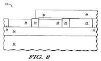
図8には、マスク40の除去およびマスク44の形成後の半導体構造10を示す。マスク44は能動領域38,28と、これもまた能動領域であるシリコン層42とを覆う。これによって、能動領域36が注入のために露出される。マスク44は完全に新しいマスクであることも可能であり、新しいマスクとマスク30との組み合わせであることも可能である。このマスクはマスク30,40を形成するのと同じように形成されてもよい。注入はN型であり、この注入によって、続くPチャネルトランジスタの形成のためのバックグラウンドドーピングが提供される。この能動領域が少なくともある程度の圧縮応力の下にあることは、Pチャネル性能に有利である。
FIG. 8 shows the
図9には、マスク44の除去、及び能動領域36,38とシリコン層42との上のマスク46の形成後の半導体構造10を示す。これによって、従来型の単結晶シリコンである能動領域28が露出される。したがって、能動領域28は最も一般的に使用される型のトランジスタを製造するために利用可能である。したがって、半導体構造10においては、一般的な大量生産におけるトランジスタ型の利点が利用可能である。
FIG. 9 shows the
図10には、能動領域36,38,28内及び上における、それぞれトランジスタ48,50,52の形成の後の半導体構造10を示す。トランジスタ50はシリコン層42内にも形成される。Pチャネルであるトランジスタ48は、能動領域36の上のゲート54、能動領域36とゲート54との間のゲート誘電体、能動領域36内の第1のソース/ドレイン58、ソース/ドレイン58から離間されている能動領域36内の第2のソース/ドレイン60、およびゲート54の周囲のサイドウォールスペーサ56からなる。ソース/ドレイン58,60はP型である。Nチャネルであるトランジスタ50は、能動領域38とシリコン層42との上のゲート62、ゲート62とシリコン層42との間のゲート誘電体66、層42および能動領域68内のソース/ドレイン68、ソース/ドレイン領域68から離間されており、かつ、能動領域38およびシリコン層42内のソース/ドレイン70、およびゲート62の周囲のサイドウォールスペーサ64からなる。ソース/ドレイン68,70はN型である。トランジスタ52はNチャネルであることもPチャネルであることも可能であり、能動領域28の上のゲート72、ゲート72と能動領域28との間のゲート誘電体76、能動領域28内のソース/ドレイン領域78、能動領域28内のソース/ドレイン80、及びゲート72の周囲のサイドウォールスペーサ74からなる。ソース/ドレイン78,80はP型であることもN型であることも可能である。トランジスタ52によって、この記載の処理へ従来のNおよびPチャネルトランジスタを比較的簡単に組み込み可能であることが示される。
FIG. 10 shows
明細書においては、本発明を特定の実施形態に関して記載した。しかしながら、添付の特許請求の範囲において述べる本発明の範囲から逸脱することなく、様々な修正および変更を行なうことが可能であることが、当業者には認識される。例えば、この手法においてゲルマニウム及びシリコンとは異なる半導体材料を用いて、この結果を達成し得る。したがって、明細書及び図面は限定的な意味ではなく例示的な意味に捉えられるものであり、そうした修正全てが本発明の範囲内に含まれることが意図されるものである。 In the specification, the invention has been described with reference to specific embodiments. However, one of ordinary skill in the art appreciates that various modifications and changes can be made without departing from the scope of the present invention as set forth in the claims below. For example, this result can be achieved using a semiconductor material different from germanium and silicon in this approach. The specification and drawings are, accordingly, to be regarded in an illustrative sense rather than a restrictive sense, and all such modifications are intended to be included within the scope of the present invention.
上述においては、利点、他の長所および課題の解決策を特定の実施形態に関して記載した。さらなる利点の一例は、シリコンゲルマニウム能動領域の形成前にトレンチ分離領域の形成が可能であることによって、シリコンゲルマニウム領域におけるトレンチ分離領域の形成に必要となり得るような、これらのトレンチ分離領域の形成に必要とされる余分な開発が存在しないことである。 In the foregoing, advantages, other advantages, and solutions to problems have been described with regard to specific embodiments. An example of a further advantage is the formation of these trench isolation regions, which may be required for the formation of trench isolation regions in the silicon germanium region, by allowing the trench isolation regions to be formed prior to the formation of silicon germanium active regions. There is no extra development needed.
Claims (26)
半導体基板を準備する基板準備工程と、
非晶質シリコンゲルマニウム含有層および多結晶シリコンゲルマニウム含有層から選択される第1の層を半導体基板の上に形成する第1層形成工程と、
第1の層を酸化させる第1層酸化工程と、第1層酸化工程は第1の層をシリコン含有酸化物層に変換し、かつ、半導体基板のうちの少なくとも一部をゲルマニウムリッチ半導体層に変換することと、からなる方法。 A method for manufacturing a semiconductor structure, comprising:
A substrate preparation step of preparing a semiconductor substrate;
A first layer forming step of forming a first layer selected from an amorphous silicon germanium-containing layer and a polycrystalline silicon germanium-containing layer on a semiconductor substrate;
The first layer oxidation step for oxidizing the first layer and the first layer oxidation step convert the first layer into a silicon-containing oxide layer, and at least a part of the semiconductor substrate becomes a germanium-rich semiconductor layer Converting, and a method comprising.
第1の層の酸化中、半導体基板の半導体層はゲルマニウムリッチ半導体層へ変換されることと、を含む請求項1に記載の方法。 The semiconductor substrate includes a buried oxide layer located below the semiconductor layer;
The method of claim 1, wherein during the oxidation of the first layer, the semiconductor layer of the semiconductor substrate is converted to a germanium rich semiconductor layer.
半導体基板のうちの前記少なくとも一部は該シリコン層を含むことと、
第1の層の酸化中、半導体基板の該シリコン層はゲルマニウムリッチ半導体層へ変換されることと、を含む請求項1に記載の方法。 The semiconductor substrate includes a silicon layer;
The at least part of the semiconductor substrate includes the silicon layer;
The method of claim 1, wherein during oxidation of the first layer, the silicon layer of the semiconductor substrate is converted to a germanium rich semiconductor layer.
ゲルマニウムリッチシリコン層はパターン形成されたマスキング層によって露出される半導体基板の部分において形成されることと、を含む請求項1に記載の方法。 Prior to the first layer forming step, forming a patterned masking layer on the semiconductor substrate;
The method of claim 1, wherein the germanium rich silicon layer is formed in a portion of the semiconductor substrate exposed by the patterned masking layer.
ゲルマニウムリッチ半導体層の上のゲート誘電体と、ゲート誘電体の上のゲートと、該半導体層のゲートの下のチャンネルと、チャンネルから側方に離間されている複数のソース/ドレイン領域とを有するトランジスタを形成する工程と、を含む請求項1に記載の方法。 Forming a semiconductor layer on the germanium-rich semiconductor layer;
A gate dielectric over the germanium-rich semiconductor layer; a gate over the gate dielectric; a channel under the gate of the semiconductor layer; and a plurality of source / drain regions spaced laterally from the channel. Forming a transistor.
シリコン層を含む半導体基板を準備する基板準備工程と、
非晶質シリコンゲルマニウム層および多結晶シリコンゲルマニウム層のうちの一方であるシリコンゲルマニウム層を半導体基板のシリコン層上に形成するシリコンゲルマニウム層形成工程と、
シリコンゲルマニウム層を酸化させて、シリコンゲルマニウム層をシリコンジオキサイドに変換し、かつ、シリコン層のうちの少なくとも一部をゲルマニウムリッチシリコンに変換するシリコンゲルマニウム層酸化工程と、からなる方法。 A method for manufacturing a semiconductor structure, comprising:
A substrate preparation step of preparing a semiconductor substrate including a silicon layer;
A silicon germanium layer forming step of forming a silicon germanium layer, which is one of an amorphous silicon germanium layer and a polycrystalline silicon germanium layer, on a silicon layer of a semiconductor substrate;
A method comprising oxidizing a silicon germanium layer, converting the silicon germanium layer to silicon dioxide, and converting at least a portion of the silicon layer to germanium rich silicon.
パターン形成されたマスキング層によって露出されるシリコン層の部分はゲルマニウムリッチシリコンへ変換されることと、を含む請求項13に記載の方法。 Prior to the silicon germanium layer forming step, forming a patterned masking layer on the silicon layer;
14. The method of claim 13, comprising converting a portion of the silicon layer exposed by the patterned masking layer to germanium rich silicon.
半導体層の上のゲート誘電体と、ゲート誘電体の上のゲートと、半導体層のゲートの下のチャンネルと、チャンネルから側方に離間されている複数のソース/ドレイン領域とを有するトランジスタを形成する工程と、を含む請求項13に記載の方法。 Forming a semiconductor layer on germanium-rich silicon;
Forming a transistor having a gate dielectric over a semiconductor layer, a gate over the gate dielectric, a channel under the gate of the semiconductor layer, and a plurality of source / drain regions laterally spaced from the channel The method of claim 13 comprising the steps of:
半導体基板を準備する基板準備工程と、
第1の化学種及び第2の化学種を含有する化合物を含む第1の層を半導体基板の上に形成する第1層形成工程と、第1の層は非晶質層および多結晶層のうちの一方であることと、
第1の層を第1の化学種を含む除去可能層に変換する第1層変換工程と、第1層変換工程は第2の化学種を下に位置する半導体基板へ移動させることと、からなる方法。 A method for manufacturing a semiconductor structure, comprising:
A substrate preparation step of preparing a semiconductor substrate;
A first layer forming step of forming a first layer including a compound containing a first chemical species and a second chemical species on a semiconductor substrate; and the first layer is an amorphous layer and a polycrystalline layer Being one of them,
A first layer converting step that converts the first layer into a removable layer that includes the first chemical species, and the first layer converting step moves the second chemical species to the underlying semiconductor substrate; How to be.
Applications Claiming Priority (2)
| Application Number | Priority Date | Filing Date | Title |
|---|---|---|---|
| US10/836,172 US7163903B2 (en) | 2004-04-30 | 2004-04-30 | Method for making a semiconductor structure using silicon germanium |
| PCT/US2005/011552 WO2005112094A2 (en) | 2004-04-30 | 2005-04-05 | Method for making a semiconductor structure using silicon germanium |
Publications (2)
| Publication Number | Publication Date |
|---|---|
| JP2007535814A true JP2007535814A (en) | 2007-12-06 |
| JP2007535814A5 JP2007535814A5 (en) | 2008-05-22 |
Family
ID=35187681
Family Applications (1)
| Application Number | Title | Priority Date | Filing Date |
|---|---|---|---|
| JP2007510751A Pending JP2007535814A (en) | 2004-04-30 | 2005-04-05 | Method of manufacturing a semiconductor structure using silicon germanium |
Country Status (7)
| Country | Link |
|---|---|
| US (2) | US7163903B2 (en) |
| EP (1) | EP1751791A4 (en) |
| JP (1) | JP2007535814A (en) |
| KR (1) | KR20070011408A (en) |
| CN (1) | CN100533679C (en) |
| TW (1) | TW200605159A (en) |
| WO (1) | WO2005112094A2 (en) |
Families Citing this family (18)
| Publication number | Priority date | Publication date | Assignee | Title |
|---|---|---|---|---|
| US7163903B2 (en) * | 2004-04-30 | 2007-01-16 | Freescale Semiconductor, Inc. | Method for making a semiconductor structure using silicon germanium |
| US7332443B2 (en) * | 2005-03-18 | 2008-02-19 | Infineon Technologies Ag | Method for fabricating a semiconductor device |
| US7439165B2 (en) * | 2005-04-06 | 2008-10-21 | Agency For Sceince, Technology And Reasearch | Method of fabricating tensile strained layers and compressive strain layers for a CMOS device |
| US7420202B2 (en) | 2005-11-08 | 2008-09-02 | Freescale Semiconductor, Inc. | Electronic device including a transistor structure having an active region adjacent to a stressor layer and a process for forming the electronic device |
| US7265004B2 (en) * | 2005-11-14 | 2007-09-04 | Freescale Semiconductor, Inc. | Electronic devices including a semiconductor layer and a process for forming the same |
| US7560318B2 (en) * | 2006-03-13 | 2009-07-14 | Freescale Semiconductor, Inc. | Process for forming an electronic device including semiconductor layers having different stresses |
| US7882382B2 (en) * | 2006-06-14 | 2011-02-01 | International Business Machines Corporation | System and method for performing computer system maintenance and service |
| US7629220B2 (en) * | 2006-06-30 | 2009-12-08 | Freescale Semiconductor, Inc. | Method for forming a semiconductor device and structure thereof |
| US8569858B2 (en) | 2006-12-20 | 2013-10-29 | Freescale Semiconductor, Inc. | Semiconductor device including an active region and two layers having different stress characteristics |
| US7843011B2 (en) | 2007-01-31 | 2010-11-30 | Freescale Semiconductor, Inc. | Electronic device including insulating layers having different strains |
| FR2925979A1 (en) * | 2007-12-27 | 2009-07-03 | Commissariat Energie Atomique | METHOD FOR MANUFACTURING A SEMICONDUCTOR SUBSTRATE ON INSULATION INCLUDING AN ENRICHMENT STEP IN LOCALIZED GE |
| US8211786B2 (en) | 2008-02-28 | 2012-07-03 | International Business Machines Corporation | CMOS structure including non-planar hybrid orientation substrate with planar gate electrodes and method for fabrication |
| US20090289280A1 (en) * | 2008-05-22 | 2009-11-26 | Da Zhang | Method for Making Transistors and the Device Thereof |
| US8003454B2 (en) * | 2008-05-22 | 2011-08-23 | Freescale Semiconductor, Inc. | CMOS process with optimized PMOS and NMOS transistor devices |
| JP2010182841A (en) * | 2009-02-05 | 2010-08-19 | Sony Corp | Method of forming semiconductor thin film and inspection device for semiconductor thin film |
| US8828851B2 (en) * | 2012-02-01 | 2014-09-09 | Stmicroeletronics, Inc. | Method to enable the formation of silicon germanium channel of FDSOI devices for PFET threshold voltage engineering |
| CN103839891A (en) * | 2012-11-26 | 2014-06-04 | 中国科学院微电子研究所 | Semiconductor structure and method for manufacturing semiconductor structure |
| FR3088481A1 (en) * | 2018-11-14 | 2020-05-15 | Commissariat A L'energie Atomique Et Aux Energies Alternatives | METHOD FOR MANUFACTURING A FIELD-JUNCTION FIELD-EFFECT TRANSISTOR WITH SPACERS |
Citations (4)
| Publication number | Priority date | Publication date | Assignee | Title |
|---|---|---|---|---|
| JP2001217430A (en) * | 1999-11-26 | 2001-08-10 | Toshiba Corp | Method of manufacturing semiconductor substrate and semiconductor substrate manufactured thereby |
| JP2002305293A (en) * | 2001-04-06 | 2002-10-18 | Canon Inc | Method of manufacturing semiconductor member, and method of manufacturing semiconductor device |
| JP2003031495A (en) * | 2001-07-12 | 2003-01-31 | Hitachi Ltd | Manufacturing method of semiconductor device substrate and semiconductor device |
| JP2004063780A (en) * | 2002-07-29 | 2004-02-26 | Toshiba Corp | Method of manufacturing semiconductor device |
Family Cites Families (13)
| Publication number | Priority date | Publication date | Assignee | Title |
|---|---|---|---|---|
| US5312766A (en) | 1991-03-06 | 1994-05-17 | National Semiconductor Corporation | Method of providing lower contact resistance in MOS transistors |
| US20010003381A1 (en) * | 1998-05-20 | 2001-06-14 | Marius Orlowski | Method to locate particles of a predetermined species within a solid and resulting structures |
| JP3884203B2 (en) | 1998-12-24 | 2007-02-21 | 株式会社東芝 | Manufacturing method of semiconductor device |
| US6369438B1 (en) | 1998-12-24 | 2002-04-09 | Kabushiki Kaisha Toshiba | Semiconductor device and method for manufacturing the same |
| JP3647777B2 (en) | 2001-07-06 | 2005-05-18 | 株式会社東芝 | Method of manufacturing field effect transistor and integrated circuit element |
| US20030096490A1 (en) * | 2001-11-16 | 2003-05-22 | John Borland | Method of forming ultra shallow junctions |
| US6805962B2 (en) * | 2002-01-23 | 2004-10-19 | International Business Machines Corporation | Method of creating high-quality relaxed SiGe-on-insulator for strained Si CMOS applications |
| US6759712B2 (en) * | 2002-09-12 | 2004-07-06 | Micron Technology, Inc. | Semiconductor-on-insulator thin film transistor constructions |
| US6998683B2 (en) * | 2002-10-03 | 2006-02-14 | Micron Technology, Inc. | TFT-based common gate CMOS inverters, and computer systems utilizing novel CMOS inverters |
| US6764883B1 (en) * | 2003-01-07 | 2004-07-20 | International Business Machines Corp. | Amorphous and polycrystalline silicon nanolaminate |
| US7042052B2 (en) * | 2003-02-10 | 2006-05-09 | Micron Technology, Inc. | Transistor constructions and electronic devices |
| US7163903B2 (en) * | 2004-04-30 | 2007-01-16 | Freescale Semiconductor, Inc. | Method for making a semiconductor structure using silicon germanium |
| US7312128B2 (en) | 2004-12-01 | 2007-12-25 | Applied Materials, Inc. | Selective epitaxy process with alternating gas supply |
-
2004
- 2004-04-30 US US10/836,172 patent/US7163903B2/en not_active Expired - Fee Related
-
2005
- 2005-04-05 WO PCT/US2005/011552 patent/WO2005112094A2/en active Application Filing
- 2005-04-05 EP EP05732886A patent/EP1751791A4/en not_active Withdrawn
- 2005-04-05 JP JP2007510751A patent/JP2007535814A/en active Pending
- 2005-04-05 KR KR1020067022481A patent/KR20070011408A/en not_active Application Discontinuation
- 2005-04-05 CN CNB2005800116543A patent/CN100533679C/en not_active Expired - Fee Related
- 2005-04-22 TW TW094112960A patent/TW200605159A/en unknown
-
2006
- 2006-12-12 US US11/609,664 patent/US7927956B2/en not_active Expired - Fee Related
Patent Citations (4)
| Publication number | Priority date | Publication date | Assignee | Title |
|---|---|---|---|---|
| JP2001217430A (en) * | 1999-11-26 | 2001-08-10 | Toshiba Corp | Method of manufacturing semiconductor substrate and semiconductor substrate manufactured thereby |
| JP2002305293A (en) * | 2001-04-06 | 2002-10-18 | Canon Inc | Method of manufacturing semiconductor member, and method of manufacturing semiconductor device |
| JP2003031495A (en) * | 2001-07-12 | 2003-01-31 | Hitachi Ltd | Manufacturing method of semiconductor device substrate and semiconductor device |
| JP2004063780A (en) * | 2002-07-29 | 2004-02-26 | Toshiba Corp | Method of manufacturing semiconductor device |
Also Published As
| Publication number | Publication date |
|---|---|
| EP1751791A2 (en) | 2007-02-14 |
| TW200605159A (en) | 2006-02-01 |
| WO2005112094A2 (en) | 2005-11-24 |
| CN101147243A (en) | 2008-03-19 |
| WO2005112094A9 (en) | 2009-04-30 |
| WO2005112094A3 (en) | 2007-06-28 |
| KR20070011408A (en) | 2007-01-24 |
| US7163903B2 (en) | 2007-01-16 |
| EP1751791A4 (en) | 2010-02-03 |
| CN100533679C (en) | 2009-08-26 |
| US20070082453A1 (en) | 2007-04-12 |
| US20050245092A1 (en) | 2005-11-03 |
| US7927956B2 (en) | 2011-04-19 |
Similar Documents
| Publication | Publication Date | Title |
|---|---|---|
| JP2007535814A (en) | Method of manufacturing a semiconductor structure using silicon germanium | |
| US7960794B2 (en) | Non-planar pMOS structure with a strained channel region and an integrated strained CMOS flow | |
| US7531438B2 (en) | Method of fabricating a recess channel transistor | |
| US7417250B1 (en) | Strained-silicon device with different silicon thicknesses | |
| CN105206574A (en) | Transistor With Threshold Voltage Set Notch And Method Of Fabrication Thereof | |
| JP4177775B2 (en) | Semiconductor substrate, manufacturing method thereof, and semiconductor device | |
| KR20010110769A (en) | SEMICONDUCTOR DEVICE WITH AN INTEGRATED CMOS CIRCUIT WITH MOS TRANSISTORS HAVING SILICON-GERMANIUM (Si1-xGex) GATE ELECTRODES, AND METHOD OF MANUFACTURING SAME | |
| US20030219938A1 (en) | CMOS gate electrode using selective growth and a fabrication method thereof | |
| US7425488B2 (en) | Method and structure using a pure silicon dioxide hardmask for gate patterning for strained silicon MOS transistors | |
| CA2008499C (en) | Method for formation of an isolating oxide layer | |
| JPH0955422A (en) | Element isolation method of semiconductor element | |
| JPH0312785B2 (en) | ||
| KR101179515B1 (en) | Method of manufacturing semiconductor device | |
| US7569438B2 (en) | Method of manufacturing semiconductor device | |
| JP2005327867A (en) | Semiconductor device and method for manufacturing same | |
| JPH11163317A (en) | Semiconductor device and its manufacture | |
| JPS58190040A (en) | Preparation of semiconductor device | |
| KR20020002060A (en) | Method of fabricating soi device having double gate | |
| JPH0423828B2 (en) | ||
| KR100476666B1 (en) | Method for manufacturing semiconductor device | |
| JPH0529310A (en) | Manufacture of semiconductor device | |
| KR20040060118A (en) | Method for manufacturing semiconductor device | |
| JPH04321233A (en) | Manufacture of semiconductor device | |
| JPH0450748B2 (en) | ||
| JPS61268038A (en) | Manufacture of semiconductor device |
Legal Events
| Date | Code | Title | Description |
|---|---|---|---|
| A521 | Request for written amendment filed |
Free format text: JAPANESE INTERMEDIATE CODE: A523 Effective date: 20080404 |
|
| A621 | Written request for application examination |
Free format text: JAPANESE INTERMEDIATE CODE: A621 Effective date: 20080404 |
|
| A977 | Report on retrieval |
Free format text: JAPANESE INTERMEDIATE CODE: A971007 Effective date: 20101119 |
|
| A131 | Notification of reasons for refusal |
Free format text: JAPANESE INTERMEDIATE CODE: A131 Effective date: 20101130 |
|
| A521 | Request for written amendment filed |
Free format text: JAPANESE INTERMEDIATE CODE: A523 Effective date: 20110228 |
|
| A02 | Decision of refusal |
Free format text: JAPANESE INTERMEDIATE CODE: A02 Effective date: 20111206 |