JP2007514316A - Soiボディコンタクトトランジスタを製造する方法及び装置 - Google Patents
Soiボディコンタクトトランジスタを製造する方法及び装置 Download PDFInfo
- Publication number
- JP2007514316A JP2007514316A JP2006543827A JP2006543827A JP2007514316A JP 2007514316 A JP2007514316 A JP 2007514316A JP 2006543827 A JP2006543827 A JP 2006543827A JP 2006543827 A JP2006543827 A JP 2006543827A JP 2007514316 A JP2007514316 A JP 2007514316A
- Authority
- JP
- Japan
- Prior art keywords
- region
- coupled
- gate electrode
- forming
- access region
- Prior art date
- Legal status (The legal status is an assumption and is not a legal conclusion. Google has not performed a legal analysis and makes no representation as to the accuracy of the status listed.)
- Pending
Links
- 238000000034 method Methods 0.000 title claims abstract description 45
- 238000004519 manufacturing process Methods 0.000 title claims abstract description 10
- 230000008878 coupling Effects 0.000 claims abstract description 81
- 238000010168 coupling process Methods 0.000 claims abstract description 81
- 238000005859 coupling reaction Methods 0.000 claims abstract description 81
- 210000000746 body region Anatomy 0.000 claims abstract description 54
- 238000009792 diffusion process Methods 0.000 claims abstract description 53
- 239000012212 insulator Substances 0.000 claims abstract description 33
- 230000003071 parasitic effect Effects 0.000 claims abstract description 9
- 125000006850 spacer group Chemical group 0.000 claims description 28
- 150000003377 silicon compounds Chemical class 0.000 claims description 23
- 239000007772 electrode material Substances 0.000 claims description 16
- 239000007943 implant Substances 0.000 claims description 11
- 238000002513 implantation Methods 0.000 claims description 9
- 230000015572 biosynthetic process Effects 0.000 claims description 8
- 239000002019 doping agent Substances 0.000 claims description 6
- 239000000463 material Substances 0.000 claims description 6
- 239000003989 dielectric material Substances 0.000 claims description 5
- 125000001475 halogen functional group Chemical group 0.000 claims description 5
- 230000000903 blocking effect Effects 0.000 claims description 4
- 230000000873 masking effect Effects 0.000 claims description 3
- 239000000758 substrate Substances 0.000 claims description 3
- 239000004020 conductor Substances 0.000 claims description 2
- 238000000151 deposition Methods 0.000 claims description 2
- 238000000059 patterning Methods 0.000 claims description 2
- 229910021420 polycrystalline silicon Inorganic materials 0.000 description 17
- 229920005591 polysilicon Polymers 0.000 description 17
- 238000002955 isolation Methods 0.000 description 10
- 230000008901 benefit Effects 0.000 description 7
- 230000008569 process Effects 0.000 description 6
- XUIMIQQOPSSXEZ-UHFFFAOYSA-N Silicon Chemical compound [Si] XUIMIQQOPSSXEZ-UHFFFAOYSA-N 0.000 description 5
- 229910052710 silicon Inorganic materials 0.000 description 5
- 239000010703 silicon Substances 0.000 description 5
- 238000010586 diagram Methods 0.000 description 4
- 238000013329 compounding Methods 0.000 description 3
- 230000009977 dual effect Effects 0.000 description 3
- 239000004065 semiconductor Substances 0.000 description 3
- 238000012986 modification Methods 0.000 description 2
- 230000004048 modification Effects 0.000 description 2
- VYPSYNLAJGMNEJ-UHFFFAOYSA-N Silicium dioxide Chemical compound O=[Si]=O VYPSYNLAJGMNEJ-UHFFFAOYSA-N 0.000 description 1
- 230000008859 change Effects 0.000 description 1
- 230000000295 complement effect Effects 0.000 description 1
- 230000000694 effects Effects 0.000 description 1
- 238000005516 engineering process Methods 0.000 description 1
- 150000004767 nitrides Chemical class 0.000 description 1
- 230000010363 phase shift Effects 0.000 description 1
- 230000009467 reduction Effects 0.000 description 1
- 229910052814 silicon oxide Inorganic materials 0.000 description 1
Images


Classifications
-
- H—ELECTRICITY
- H01—ELECTRIC ELEMENTS
- H01L—SEMICONDUCTOR DEVICES NOT COVERED BY CLASS H10
- H01L27/00—Devices consisting of a plurality of semiconductor or other solid-state components formed in or on a common substrate
- H01L27/02—Devices consisting of a plurality of semiconductor or other solid-state components formed in or on a common substrate including semiconductor components specially adapted for rectifying, oscillating, amplifying or switching and having at least one potential-jump barrier or surface barrier; including integrated passive circuit elements with at least one potential-jump barrier or surface barrier
- H01L27/12—Devices consisting of a plurality of semiconductor or other solid-state components formed in or on a common substrate including semiconductor components specially adapted for rectifying, oscillating, amplifying or switching and having at least one potential-jump barrier or surface barrier; including integrated passive circuit elements with at least one potential-jump barrier or surface barrier the substrate being other than a semiconductor body, e.g. an insulating body
-
- H—ELECTRICITY
- H01—ELECTRIC ELEMENTS
- H01L—SEMICONDUCTOR DEVICES NOT COVERED BY CLASS H10
- H01L29/00—Semiconductor devices adapted for rectifying, amplifying, oscillating or switching, or capacitors or resistors with at least one potential-jump barrier or surface barrier, e.g. PN junction depletion layer or carrier concentration layer; Details of semiconductor bodies or of electrodes thereof ; Multistep manufacturing processes therefor
- H01L29/66—Types of semiconductor device ; Multistep manufacturing processes therefor
- H01L29/66007—Multistep manufacturing processes
- H01L29/66075—Multistep manufacturing processes of devices having semiconductor bodies comprising group 14 or group 13/15 materials
- H01L29/66227—Multistep manufacturing processes of devices having semiconductor bodies comprising group 14 or group 13/15 materials the devices being controllable only by the electric current supplied or the electric potential applied, to an electrode which does not carry the current to be rectified, amplified or switched, e.g. three-terminal devices
- H01L29/66409—Unipolar field-effect transistors
- H01L29/66477—Unipolar field-effect transistors with an insulated gate, i.e. MISFET
- H01L29/66742—Thin film unipolar transistors
- H01L29/66772—Monocristalline silicon transistors on insulating substrates, e.g. quartz substrates
-
- H—ELECTRICITY
- H01—ELECTRIC ELEMENTS
- H01L—SEMICONDUCTOR DEVICES NOT COVERED BY CLASS H10
- H01L21/00—Processes or apparatus adapted for the manufacture or treatment of semiconductor or solid state devices or of parts thereof
- H01L21/02—Manufacture or treatment of semiconductor devices or of parts thereof
- H01L21/04—Manufacture or treatment of semiconductor devices or of parts thereof the devices having at least one potential-jump barrier or surface barrier, e.g. PN junction, depletion layer or carrier concentration layer
- H01L21/18—Manufacture or treatment of semiconductor devices or of parts thereof the devices having at least one potential-jump barrier or surface barrier, e.g. PN junction, depletion layer or carrier concentration layer the devices having semiconductor bodies comprising elements of Group IV of the Periodic System or AIIIBV compounds with or without impurities, e.g. doping materials
-
- H—ELECTRICITY
- H01—ELECTRIC ELEMENTS
- H01L—SEMICONDUCTOR DEVICES NOT COVERED BY CLASS H10
- H01L29/00—Semiconductor devices adapted for rectifying, amplifying, oscillating or switching, or capacitors or resistors with at least one potential-jump barrier or surface barrier, e.g. PN junction depletion layer or carrier concentration layer; Details of semiconductor bodies or of electrodes thereof ; Multistep manufacturing processes therefor
- H01L29/40—Electrodes ; Multistep manufacturing processes therefor
- H01L29/43—Electrodes ; Multistep manufacturing processes therefor characterised by the materials of which they are formed
- H01L29/45—Ohmic electrodes
- H01L29/456—Ohmic electrodes on silicon
- H01L29/458—Ohmic electrodes on silicon for thin film silicon, e.g. source or drain electrode
-
- H—ELECTRICITY
- H01—ELECTRIC ELEMENTS
- H01L—SEMICONDUCTOR DEVICES NOT COVERED BY CLASS H10
- H01L29/00—Semiconductor devices adapted for rectifying, amplifying, oscillating or switching, or capacitors or resistors with at least one potential-jump barrier or surface barrier, e.g. PN junction depletion layer or carrier concentration layer; Details of semiconductor bodies or of electrodes thereof ; Multistep manufacturing processes therefor
- H01L29/66—Types of semiconductor device ; Multistep manufacturing processes therefor
- H01L29/68—Types of semiconductor device ; Multistep manufacturing processes therefor controllable by only the electric current supplied, or only the electric potential applied, to an electrode which does not carry the current to be rectified, amplified or switched
- H01L29/76—Unipolar devices, e.g. field effect transistors
- H01L29/772—Field effect transistors
- H01L29/78—Field effect transistors with field effect produced by an insulated gate
- H01L29/786—Thin film transistors, i.e. transistors with a channel being at least partly a thin film
- H01L29/78606—Thin film transistors, i.e. transistors with a channel being at least partly a thin film with supplementary region or layer in the thin film or in the insulated bulk substrate supporting it for controlling or increasing the safety of the device
- H01L29/78612—Thin film transistors, i.e. transistors with a channel being at least partly a thin film with supplementary region or layer in the thin film or in the insulated bulk substrate supporting it for controlling or increasing the safety of the device for preventing the kink- or the snapback effect, e.g. discharging the minority carriers of the channel region for preventing bipolar effect
- H01L29/78615—Thin film transistors, i.e. transistors with a channel being at least partly a thin film with supplementary region or layer in the thin film or in the insulated bulk substrate supporting it for controlling or increasing the safety of the device for preventing the kink- or the snapback effect, e.g. discharging the minority carriers of the channel region for preventing bipolar effect with a body contact
Abstract
Description
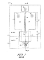
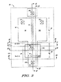
図中の要素が簡便さや明瞭さを期して示され、必ずしも実寸に従い図示されていないことは、当業者にとって明らかである。例えば、図中の構成要素の寸法は、本発明の実施形態の理解を一層深めるため、他の構成要素と比較して誇張されていることがある。
Claims (18)
- シリコンオンインシュレータトランジスタであって、
絶縁層と、
前記絶縁層上に設けられるアクティブ領域と、
そのアクティブ領域は、内部ボディ領域と、前記絶縁層上に設けられ、内部ボディ領域に横方向に隣接し、前記内部ボディ領域との電気的コンタクトを形成するボディ結合アクセス領域と、前記ボディ結合アクセス領域から横方向にオフセットされ、前記ボディ結合アクセス領域に電気的に接続されるボディ結合拡散部とを有し、
前記シリコンオンインシュレータトランジスタの前記内部ボディ領域を電気的に制御するため、前記内部ボディ領域を覆い、前記ボディ結合アクセス領域の一部を覆うように延在しているゲート電極と、
前記内部ボディ領域の対向する両側面に隣接する第1及び第2の電流電極と
を備えるシリコンオンインシュレータトランジスタ。 - 請求項1記載のシリコンオンインシュレータトランジスタにおいて、
前記ボディ結合アクセス領域を覆うゲート電極の一部を含むボディ結合アクセス領のほぼ全てを覆う誘電体層を更に備えているシリコンオンインシュレータトランジスタ。 - 請求項2記載のシリコンオンインシュレータトランジスタにおいて、
前記誘電体層は、前記ゲート電極の側壁スペーサーとして機能するシリコンオンインシュレータトランジスタ。 - 請求項2記載のシリコンオンインシュレータトランジスタにおいて、
前記誘電体層の下層にあるボディ結合アクセス領域の一部は、ボディ結合アクセス領域のドーピング濃度を高くして前記ボディ結合アクセス領域での空乏領域の形成を大幅に低減する被ドーピング材料からなるシリコンオンインシュレータトランジスタ。 - 請求項4記載のシリコンオンインシュレータトランジスタにおいて、
前記ボディ結合アクセス領域の部分的なドーピングは、前記誘電体層を形成するため、第1のマスクのパターン形状を使用し、かつ第2のマスクの前記パターンを再度使用して行われるシリコンオンインシュレータトランジスタ。 - 請求項1記載のシリコンオンインシュレータトランジスタにおいて、
前記ゲート電極は、寄生ゲート静電容量及び電流漏出を低減するため、前記ボディ結合アクセス領域の1/2を超えて延在していないシリコンオンインシュレータトランジスタ。 - シリコンオンインシュレータトランジスタの製造方法であって、
絶縁層を提供するステップ、
前記絶縁層上にアクティブ領域を形成するステップであって、前記アクティブ領域の一部が内部ボディ領域を提供するステップ、
前記アクティブ領域内において、前記絶縁層上に設けられ、前記内部ボディ領域に横方向に隣接するボディ結合アクセス領域を形成するステップであって、前記ボディ結合アクセス領域が前記内部ボディ領域との電気的コンタクトを形成するステップ、
前記シリコンオンインシュレータトランジスタの内部ボディ領域を電気的に制御するため前記内部ボディ領域上に設けられ、寄生容量及びゲート電極漏出を低減するため前記ボディ結合アクセス領域の一部を覆うように延在するゲート電極を形成するステップ、
前記内部ボディ領域の対向する両側に隣接して第1及び第2の電流電極を形成するステップ、及び
前記アクティブ領域内において、前記ボディ結合アクセス領域から横方向にずれして位置し、前記ボディ結合アクセス領域に電気的に接続されるボディ結合拡散部を形成するステップ
を備える方法。 - 請求項7記載の方法は、更に、
前記ボディ結合アクセス領域上に設けられた前記ゲート電極の部分を含む前記ボディ結合アクセス領域のほぼ全てを覆う誘電体層を形成するステップを備える方法。 - 請求項8記載の方法は、更に、
前記ボディ結合アクセス領域での空乏領域の形成を大幅に低減させるため、前記ボディ結合アクセス領域のドーピング濃度を増大させて、前記誘電体層の下層にある前記ボディ結合アクセス領域の一部をドーピングするステップを備える方法。 - 請求項9記載の方法において、
前記ドーピングするステップは、更に、前記ドーピング用の第1の選択的ブロックとして第1のマスクのパターン形状を使用し、かつ第2の選択的ブロックとして第2のマスクに同パターン形状を再度使用して前記誘電体層を提供するステップを備える方法。 - 請求項7記載の方法は、更に、
前記ボディ結合アクセス領域の1/2を超えて前記ゲート電極を延在させないことによって、寄生ゲート静電容量及び電流漏出を低減させるステップを備える方法。 - シリコンオンインシュレータトランジスタの製造方法であって、
絶縁基板を形成するステップ、
前記シリコンオンインシュレータトランジスタの位置を決めるアクティブ領域を画定するステップ、
所望のドーピング濃度の内部ボディ領域を形成するため、前記アクティブ領域に所定の拡散材料を注入するステップ、
前記アクティブ領域を覆うマスクに開口を形成してボディ結合アクセス領域を画定するステップ、
前記ボディ結合アクセス領域を形成するため前記アクティブ領域を注入するステップであって、ボディ結合アクセス抵抗を低減させるため、前記ボディ結合アクセス領域が所定のドーピング濃度を有しているステップ、
前記内部ボディ領域及び前記ボディ結合アクセス領域の両方を覆うゲート酸化物を形成するステップ、
前記内部ボディ領域及び前記ボディ結合アクセス領域の一部を覆うほぼ一定長さのゲート電極材料を成膜及びパターニングするステップ、
前記ボディ結合アクセス領域からのドーパントのハロー/拡大注入をほぼ遮断しながら、前記内部ボディ領域内へのドーパントのハロー/拡大注入を形成するステップ、
ほぼ一定長さのゲート電極材料及びボディ結合アクセス領域を覆う側壁スペーサー誘電体材料を形成するステップ、
マスクを用いて前記ボディ結合アクセス領域をほぼ覆う領域をマスキングするステップ、
前記ボディ結合アクセス領域を覆うと共に、ほぼ一定長さのゲート電極材料に隣接する部分を除くあらゆる場所で、前記側壁スペーサー誘電体材料を除去するステップ、
ソース拡散領域及びドレイン拡散領域を形成するステップ、及び
ボディ結合拡散領域を形成するステップ
を備える方法。 - 請求項12記載の方法は、更に、
前記ソース拡散領域、前記ドレイン拡散領域、前記ボディ結合拡散部及びほぼ一定長さのゲート電極材料を覆うケイ素化合物層を形成することによって、前記ソース拡散領域、前記ドレイン拡散領域、前記ボディ結合拡散部及びほぼ一定長さのゲート電極材料との電気的コンタクトを形成するステップを備える方法。 - 請求項12記載の方法は、更に、
前記ソース拡散領域及び前記ドレイン拡散領域に注入されるドーパントの前記ボディ結合拡散部内への注入を防止し、その逆も防止するのに必要な最小限の距離を有するように、前記ボディ結合アクセス領域のマスキングに使用されるマスクの寸法を規定するステップを備える方法。 - 請求項12記載の方法は、更に、
前記ソース拡散領域、前記ドレイン拡散領域、ほぼ一定長さのゲート電極材料及び前記ボディ結合拡散領域をそれぞれ選択的に覆う導電材料を成膜及び形成して、それらとの電気的コンタクトを形成するステップを備える方法。 - 請求項15記載の方法は、更に、
前記ソース拡散領域、前記ドレイン拡散領域、前記ボディ結合拡散領域及びほぼ一定長さのゲート電極材料とそれぞれ接触するケイ素化合物による電気的短絡を防止するのに十分な大きさ有するように、前記マスクの寸法を規定するステップを備える方法。 - 請求項12記載の方法は、更に、
前記マスクの使用によって、前記内部ボディ領域を覆うゲート酸化物の第2の厚さよりも大きい第1の厚さを有するように、前記ボディ結合アクセス領域上に前記ゲート酸化物を形成するステップを備える方法。 - 請求項12記載の方法は、更に、
前記ボディ結合アクセス領域の1/2未満を覆うように、ほぼ一定長さのゲート電極材料を延在させるステップを備える方法。
Applications Claiming Priority (2)
| Application Number | Priority Date | Filing Date | Title |
|---|---|---|---|
| US10/734,435 US6953738B2 (en) | 2003-12-12 | 2003-12-12 | Method and apparatus for forming an SOI body-contacted transistor |
| PCT/US2004/037760 WO2005060464A2 (en) | 2003-12-12 | 2004-11-12 | Method and apparatus for forming an soi body-contacted transistor |
Publications (2)
| Publication Number | Publication Date |
|---|---|
| JP2007514316A true JP2007514316A (ja) | 2007-05-31 |
| JP2007514316A5 JP2007514316A5 (ja) | 2007-12-27 |
Family
ID=34653364
Family Applications (1)
| Application Number | Title | Priority Date | Filing Date |
|---|---|---|---|
| JP2006543827A Pending JP2007514316A (ja) | 2003-12-12 | 2004-11-12 | Soiボディコンタクトトランジスタを製造する方法及び装置 |
Country Status (7)
| Country | Link |
|---|---|
| US (1) | US6953738B2 (ja) |
| EP (1) | EP1694615A4 (ja) |
| JP (1) | JP2007514316A (ja) |
| KR (1) | KR101113009B1 (ja) |
| CN (1) | CN1890799A (ja) |
| TW (1) | TWI358080B (ja) |
| WO (1) | WO2005060464A2 (ja) |
Cited By (1)
| Publication number | Priority date | Publication date | Assignee | Title |
|---|---|---|---|---|
| JP2010004006A (ja) * | 2008-06-18 | 2010-01-07 | Internatl Business Mach Corp <Ibm> | 寄生容量が低減されたsoiボディ・コンタクト型fetのための方法及び構造体 |
Families Citing this family (42)
| Publication number | Priority date | Publication date | Assignee | Title |
|---|---|---|---|---|
| US6804502B2 (en) | 2001-10-10 | 2004-10-12 | Peregrine Semiconductor Corporation | Switch circuit and method of switching radio frequency signals |
| EP3570374B1 (en) | 2004-06-23 | 2022-04-20 | pSemi Corporation | Integrated rf front end |
| US7244640B2 (en) * | 2004-10-19 | 2007-07-17 | Taiwan Semiconductor Manufacturing Company, Ltd. | Method for fabricating a body contact in a Finfet structure and a device including the same |
| US9653601B2 (en) | 2005-07-11 | 2017-05-16 | Peregrine Semiconductor Corporation | Method and apparatus for use in improving linearity of MOSFETs using an accumulated charge sink-harmonic wrinkle reduction |
| US20080076371A1 (en) | 2005-07-11 | 2008-03-27 | Alexander Dribinsky | Circuit and method for controlling charge injection in radio frequency switches |
| US8742502B2 (en) | 2005-07-11 | 2014-06-03 | Peregrine Semiconductor Corporation | Method and apparatus for use in improving linearity of MOSFETs using an accumulated charge sink-harmonic wrinkle reduction |
| US7890891B2 (en) | 2005-07-11 | 2011-02-15 | Peregrine Semiconductor Corporation | Method and apparatus improving gate oxide reliability by controlling accumulated charge |
| USRE48965E1 (en) | 2005-07-11 | 2022-03-08 | Psemi Corporation | Method and apparatus improving gate oxide reliability by controlling accumulated charge |
| US7910993B2 (en) | 2005-07-11 | 2011-03-22 | Peregrine Semiconductor Corporation | Method and apparatus for use in improving linearity of MOSFET's using an accumulated charge sink |
| US7446001B2 (en) * | 2006-02-08 | 2008-11-04 | Freescale Semiconductors, Inc. | Method for forming a semiconductor-on-insulator (SOI) body-contacted device with a portion of drain region removed |
| US7855414B2 (en) * | 2006-07-28 | 2010-12-21 | Broadcom Corporation | Semiconductor device with increased breakdown voltage |
| US8587062B2 (en) * | 2007-03-26 | 2013-11-19 | International Business Machines Corporation | Silicon on insulator (SOI) field effect transistors (FETs) with adjacent body contacts |
| US7679139B2 (en) * | 2007-09-11 | 2010-03-16 | Honeywell International Inc. | Non-planar silicon-on-insulator device that includes an “area-efficient” body tie |
| EP2255443B1 (en) | 2008-02-28 | 2012-11-28 | Peregrine Semiconductor Corporation | Method and apparatus for use in digitally tuning a capacitor in an integrated circuit device |
| US20090236632A1 (en) * | 2008-03-19 | 2009-09-24 | Anderson Brent A | Fet having high-k, vt modifying channel and gate extension devoid of high-k and/or vt modifying material, and design structure |
| US8410554B2 (en) * | 2008-03-26 | 2013-04-02 | International Business Machines Corporation | Method, structure and design structure for customizing history effects of SOI circuits |
| US8420460B2 (en) | 2008-03-26 | 2013-04-16 | International Business Machines Corporation | Method, structure and design structure for customizing history effects of SOI circuits |
| US7964467B2 (en) * | 2008-03-26 | 2011-06-21 | International Business Machines Corporation | Method, structure and design structure for customizing history effects of soi circuits |
| US7820530B2 (en) | 2008-10-01 | 2010-10-26 | Freescale Semiconductor, Inc. | Efficient body contact field effect transistor with reduced body resistance |
| US8723260B1 (en) | 2009-03-12 | 2014-05-13 | Rf Micro Devices, Inc. | Semiconductor radio frequency switch with body contact |
| US8680617B2 (en) * | 2009-10-06 | 2014-03-25 | International Business Machines Corporation | Split level shallow trench isolation for area efficient body contacts in SOI MOSFETS |
| US8441071B2 (en) * | 2010-01-05 | 2013-05-14 | International Business Machines Corporation | Body contacted transistor with reduced parasitic capacitance |
| US8426917B2 (en) * | 2010-01-07 | 2013-04-23 | International Business Machines Corporation | Body-tied asymmetric P-type field effect transistor |
| US8643107B2 (en) * | 2010-01-07 | 2014-02-04 | International Business Machines Corporation | Body-tied asymmetric N-type field effect transistor |
| US8299519B2 (en) * | 2010-01-11 | 2012-10-30 | International Business Machines Corporation | Read transistor for single poly non-volatile memory using body contacted SOI device |
| US8283722B2 (en) | 2010-06-14 | 2012-10-09 | Broadcom Corporation | Semiconductor device having an enhanced well region |
| DE112011103554T5 (de) * | 2010-10-20 | 2013-09-05 | Peregrine Semiconductor Corp. | Verfahren und Vorrichtung zur Verwendung bei der Verbesserung einer Linearität von Mosfets unter Verwendung einer Ladungsakkumulationssenke - Reduktion harmonischer Falten |
| JP5521993B2 (ja) * | 2010-11-17 | 2014-06-18 | 富士通セミコンダクター株式会社 | 半導体装置の製造方法及び半導体装置 |
| US9123807B2 (en) * | 2010-12-28 | 2015-09-01 | Broadcom Corporation | Reduction of parasitic capacitance in a semiconductor device |
| US8217456B1 (en) | 2011-03-11 | 2012-07-10 | International Business Machines Corporation | Low capacitance hi-K dual work function metal gate body-contacted field effect transistor |
| US9590674B2 (en) | 2012-12-14 | 2017-03-07 | Peregrine Semiconductor Corporation | Semiconductor devices with switchable ground-body connection |
| US20150236798A1 (en) | 2013-03-14 | 2015-08-20 | Peregrine Semiconductor Corporation | Methods for Increasing RF Throughput Via Usage of Tunable Filters |
| US9111801B2 (en) | 2013-04-04 | 2015-08-18 | Stmicroelectronics, Inc. | Integrated circuit devices and fabrication techniques |
| US9406695B2 (en) | 2013-11-20 | 2016-08-02 | Peregrine Semiconductor Corporation | Circuit and method for improving ESD tolerance and switching speed |
| US9831857B2 (en) | 2015-03-11 | 2017-11-28 | Peregrine Semiconductor Corporation | Power splitter with programmable output phase shift |
| US9948281B2 (en) | 2016-09-02 | 2018-04-17 | Peregrine Semiconductor Corporation | Positive logic digitally tunable capacitor |
| US10587263B2 (en) * | 2016-12-14 | 2020-03-10 | Hitachi Automotive Systems, Ltd. | Load drive apparatus |
| EP3654385A4 (en) * | 2017-08-07 | 2020-11-18 | TowerJazz Panasonic Semiconductor Co., Ltd. | SEMICONDUCTOR COMPONENT |
| US10886911B2 (en) | 2018-03-28 | 2021-01-05 | Psemi Corporation | Stacked FET switch bias ladders |
| US10236872B1 (en) | 2018-03-28 | 2019-03-19 | Psemi Corporation | AC coupling modules for bias ladders |
| US10505530B2 (en) | 2018-03-28 | 2019-12-10 | Psemi Corporation | Positive logic switch with selectable DC blocking circuit |
| US11476849B2 (en) | 2020-01-06 | 2022-10-18 | Psemi Corporation | High power positive logic switch |
Citations (2)
| Publication number | Priority date | Publication date | Assignee | Title |
|---|---|---|---|---|
| JP2002231956A (ja) * | 2001-02-01 | 2002-08-16 | Matsushita Electric Ind Co Ltd | 半導体装置及びその製造方法 |
| JP2002261292A (ja) * | 2000-12-26 | 2002-09-13 | Toshiba Corp | 半導体装置及びその製造方法 |
Family Cites Families (3)
| Publication number | Priority date | Publication date | Assignee | Title |
|---|---|---|---|---|
| US6353245B1 (en) * | 1998-04-09 | 2002-03-05 | Texas Instruments Incorporated | Body-tied-to-source partially depleted SOI MOSFET |
| JP4614522B2 (ja) | 2000-10-25 | 2011-01-19 | 富士通セミコンダクター株式会社 | 半導体装置及びその製造方法 |
| US6620656B2 (en) * | 2001-12-19 | 2003-09-16 | Motorola, Inc. | Method of forming body-tied silicon on insulator semiconductor device |
-
2003
- 2003-12-12 US US10/734,435 patent/US6953738B2/en not_active Expired - Lifetime
-
2004
- 2004-11-12 JP JP2006543827A patent/JP2007514316A/ja active Pending
- 2004-11-12 EP EP04810814A patent/EP1694615A4/en not_active Withdrawn
- 2004-11-12 CN CNA200480036861XA patent/CN1890799A/zh active Pending
- 2004-11-12 KR KR1020067011511A patent/KR101113009B1/ko not_active IP Right Cessation
- 2004-11-12 WO PCT/US2004/037760 patent/WO2005060464A2/en active Application Filing
- 2004-12-10 TW TW093138451A patent/TWI358080B/zh not_active IP Right Cessation
Patent Citations (2)
| Publication number | Priority date | Publication date | Assignee | Title |
|---|---|---|---|---|
| JP2002261292A (ja) * | 2000-12-26 | 2002-09-13 | Toshiba Corp | 半導体装置及びその製造方法 |
| JP2002231956A (ja) * | 2001-02-01 | 2002-08-16 | Matsushita Electric Ind Co Ltd | 半導体装置及びその製造方法 |
Cited By (3)
| Publication number | Priority date | Publication date | Assignee | Title |
|---|---|---|---|---|
| JP2010004006A (ja) * | 2008-06-18 | 2010-01-07 | Internatl Business Mach Corp <Ibm> | 寄生容量が低減されたsoiボディ・コンタクト型fetのための方法及び構造体 |
| JP2010258471A (ja) * | 2008-06-18 | 2010-11-11 | Internatl Business Mach Corp <Ibm> | 寄生容量が低減されたsoiボディ・コンタクト型fetのための方法 |
| US7893494B2 (en) | 2008-06-18 | 2011-02-22 | International Business Machines Corporation | Method and structure for SOI body contact FET with reduced parasitic capacitance |
Also Published As
| Publication number | Publication date |
|---|---|
| KR101113009B1 (ko) | 2012-02-24 |
| WO2005060464A3 (en) | 2005-11-17 |
| WO2005060464A2 (en) | 2005-07-07 |
| CN1890799A (zh) | 2007-01-03 |
| TWI358080B (en) | 2012-02-11 |
| EP1694615A4 (en) | 2009-09-23 |
| US20050127442A1 (en) | 2005-06-16 |
| US6953738B2 (en) | 2005-10-11 |
| KR20070003787A (ko) | 2007-01-05 |
| TW200534340A (en) | 2005-10-16 |
| EP1694615A2 (en) | 2006-08-30 |
Similar Documents
| Publication | Publication Date | Title |
|---|---|---|
| JP2007514316A (ja) | Soiボディコンタクトトランジスタを製造する方法及び装置 | |
| KR100189966B1 (ko) | 소이 구조의 모스 트랜지스터 및 그 제조방법 | |
| US6392271B1 (en) | Structure and process flow for fabrication of dual gate floating body integrated MOS transistors | |
| TWI287867B (en) | Independently accessed double-gate and tri-gate transistors in same process flow | |
| KR20040065297A (ko) | 본체결합식 실리콘-온-인슐레이터 반도체 디바이스 및 그제조방법 | |
| JP3455452B2 (ja) | 半導体デバイス及びその製造方法 | |
| KR20000022709A (ko) | 전계 효과 트랜지스터와 반도체 구조물 및 그의 제조 방법 | |
| EP1335425A1 (en) | Semiconductor device and its production method | |
| JP2010536169A (ja) | 金属ゲート及び高k誘電体を有する回路構造体 | |
| US6555446B1 (en) | Body contact silicon-on-insulator transistor and method | |
| KR20070083207A (ko) | 반도체 장치 | |
| US9425189B1 (en) | Compact FDSOI device with Bulex contact extending through buried insulating layer adjacent gate structure for back-bias | |
| US20020175380A1 (en) | Cmos with a fixed charge in the gate dielectric | |
| US7307320B2 (en) | Differential mechanical stress-producing regions for integrated circuit field effect transistors | |
| US7399670B2 (en) | Methods of forming different gate structures in NMOS and PMOS regions and gate structures so formed | |
| KR100457222B1 (ko) | 고전압 소자의 제조방법 | |
| JP2004072063A (ja) | 半導体装置及びその製造方法 | |
| JPH10335484A (ja) | 半導体装置の製造方法 | |
| KR100424414B1 (ko) | 고전압 트랜지스터 형성방법 | |
| JPH10163338A (ja) | 半導体装置とその製造方法 | |
| KR20000066568A (ko) | 반도체 소자의 제조방법 | |
| JP4265890B2 (ja) | 絶縁ゲート型電界効果トランジスタの製造方法 | |
| JPH04115538A (ja) | 半導体装置 | |
| JPH08250726A (ja) | 絶縁ゲート型電界効果トランジスタおよびその製造方法 | |
| JP2004103637A (ja) | 半導体装置およびその製造方法 |
Legal Events
| Date | Code | Title | Description |
|---|---|---|---|
| A521 | Request for written amendment filed |
Free format text: JAPANESE INTERMEDIATE CODE: A523 Effective date: 20071109 |
|
| A621 | Written request for application examination |
Free format text: JAPANESE INTERMEDIATE CODE: A621 Effective date: 20071109 |
|
| A131 | Notification of reasons for refusal |
Free format text: JAPANESE INTERMEDIATE CODE: A131 Effective date: 20110824 |
|
| A977 | Report on retrieval |
Free format text: JAPANESE INTERMEDIATE CODE: A971007 Effective date: 20110825 |
|
| A601 | Written request for extension of time |
Free format text: JAPANESE INTERMEDIATE CODE: A601 Effective date: 20111124 |
|
| A602 | Written permission of extension of time |
Free format text: JAPANESE INTERMEDIATE CODE: A602 Effective date: 20111201 |
|
| A521 | Request for written amendment filed |
Free format text: JAPANESE INTERMEDIATE CODE: A523 Effective date: 20111222 |
|
| A131 | Notification of reasons for refusal |
Free format text: JAPANESE INTERMEDIATE CODE: A131 Effective date: 20120515 |
|
| A601 | Written request for extension of time |
Free format text: JAPANESE INTERMEDIATE CODE: A601 Effective date: 20120810 |
|
| A602 | Written permission of extension of time |
Free format text: JAPANESE INTERMEDIATE CODE: A602 Effective date: 20120817 |
|
| A601 | Written request for extension of time |
Free format text: JAPANESE INTERMEDIATE CODE: A601 Effective date: 20120914 |
|
| A602 | Written permission of extension of time |
Free format text: JAPANESE INTERMEDIATE CODE: A602 Effective date: 20120924 |
|
| A521 | Request for written amendment filed |
Free format text: JAPANESE INTERMEDIATE CODE: A523 Effective date: 20121012 |
|
| A02 | Decision of refusal |
Free format text: JAPANESE INTERMEDIATE CODE: A02 Effective date: 20130409 |