JP2007288201A - 均質性が改善された側壁スペーサを備えたメモリセル - Google Patents
均質性が改善された側壁スペーサを備えたメモリセル Download PDFInfo
- Publication number
- JP2007288201A JP2007288201A JP2007109542A JP2007109542A JP2007288201A JP 2007288201 A JP2007288201 A JP 2007288201A JP 2007109542 A JP2007109542 A JP 2007109542A JP 2007109542 A JP2007109542 A JP 2007109542A JP 2007288201 A JP2007288201 A JP 2007288201A
- Authority
- JP
- Japan
- Prior art keywords
- phase change
- layer
- electrode
- memory cell
- change material
- Prior art date
- Legal status (The legal status is an assumption and is not a legal conclusion. Google has not performed a legal analysis and makes no representation as to the accuracy of the status listed.)
- Pending
Links
Images







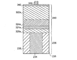

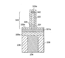

Classifications
-
- H—ELECTRICITY
- H10—SEMICONDUCTOR DEVICES; ELECTRIC SOLID-STATE DEVICES NOT OTHERWISE PROVIDED FOR
- H10N—ELECTRIC SOLID-STATE DEVICES NOT OTHERWISE PROVIDED FOR
- H10N70/00—Solid-state devices having no potential barriers, and specially adapted for rectifying, amplifying, oscillating or switching
- H10N70/20—Multistable switching devices, e.g. memristors
- H10N70/231—Multistable switching devices, e.g. memristors based on solid-state phase change, e.g. between amorphous and crystalline phases, Ovshinsky effect
-
- H—ELECTRICITY
- H10—SEMICONDUCTOR DEVICES; ELECTRIC SOLID-STATE DEVICES NOT OTHERWISE PROVIDED FOR
- H10B—ELECTRONIC MEMORY DEVICES
- H10B63/00—Resistance change memory devices, e.g. resistive RAM [ReRAM] devices
- H10B63/30—Resistance change memory devices, e.g. resistive RAM [ReRAM] devices comprising selection components having three or more electrodes, e.g. transistors
-
- H—ELECTRICITY
- H10—SEMICONDUCTOR DEVICES; ELECTRIC SOLID-STATE DEVICES NOT OTHERWISE PROVIDED FOR
- H10D—INORGANIC ELECTRIC SEMICONDUCTOR DEVICES
- H10D64/00—Electrodes of devices having potential barriers
- H10D64/01—Manufacture or treatment
- H10D64/013—Manufacture or treatment of electrodes having a conductor capacitively coupled to a semiconductor by an insulator
- H10D64/01302—Manufacture or treatment of electrodes having a conductor capacitively coupled to a semiconductor by an insulator the insulator being formed after the semiconductor body, the semiconductor being silicon
- H10D64/01332—Making the insulator
- H10D64/01334—Making the insulator by defining the insulator using a sidewall spacer mask, a transformation under a mask or a plating at a sidewall
-
- H—ELECTRICITY
- H10—SEMICONDUCTOR DEVICES; ELECTRIC SOLID-STATE DEVICES NOT OTHERWISE PROVIDED FOR
- H10N—ELECTRIC SOLID-STATE DEVICES NOT OTHERWISE PROVIDED FOR
- H10N70/00—Solid-state devices having no potential barriers, and specially adapted for rectifying, amplifying, oscillating or switching
- H10N70/011—Manufacture or treatment of multistable switching devices
- H10N70/061—Shaping switching materials
- H10N70/063—Shaping switching materials by etching of pre-deposited switching material layers, e.g. lithography
-
- H—ELECTRICITY
- H10—SEMICONDUCTOR DEVICES; ELECTRIC SOLID-STATE DEVICES NOT OTHERWISE PROVIDED FOR
- H10N—ELECTRIC SOLID-STATE DEVICES NOT OTHERWISE PROVIDED FOR
- H10N70/00—Solid-state devices having no potential barriers, and specially adapted for rectifying, amplifying, oscillating or switching
- H10N70/801—Constructional details of multistable switching devices
- H10N70/821—Device geometry
- H10N70/826—Device geometry adapted for essentially vertical current flow, e.g. sandwich or pillar type devices
-
- H—ELECTRICITY
- H10—SEMICONDUCTOR DEVICES; ELECTRIC SOLID-STATE DEVICES NOT OTHERWISE PROVIDED FOR
- H10N—ELECTRIC SOLID-STATE DEVICES NOT OTHERWISE PROVIDED FOR
- H10N70/00—Solid-state devices having no potential barriers, and specially adapted for rectifying, amplifying, oscillating or switching
- H10N70/801—Constructional details of multistable switching devices
- H10N70/881—Switching materials
- H10N70/882—Compounds of sulfur, selenium or tellurium, e.g. chalcogenides
- H10N70/8828—Tellurides, e.g. GeSbTe
-
- H—ELECTRICITY
- H10—SEMICONDUCTOR DEVICES; ELECTRIC SOLID-STATE DEVICES NOT OTHERWISE PROVIDED FOR
- H10N—ELECTRIC SOLID-STATE DEVICES NOT OTHERWISE PROVIDED FOR
- H10N70/00—Solid-state devices having no potential barriers, and specially adapted for rectifying, amplifying, oscillating or switching
- H10N70/801—Constructional details of multistable switching devices
- H10N70/881—Switching materials
- H10N70/884—Switching materials based on at least one element of group IIIA, IVA or VA, e.g. elemental or compound semiconductors
Landscapes
- Engineering & Computer Science (AREA)
- Manufacturing & Machinery (AREA)
- Semiconductor Memories (AREA)
Applications Claiming Priority (1)
| Application Number | Priority Date | Filing Date | Title |
|---|---|---|---|
| US11/406,766 US8896045B2 (en) | 2006-04-19 | 2006-04-19 | Integrated circuit including sidewall spacer |
Publications (1)
| Publication Number | Publication Date |
|---|---|
| JP2007288201A true JP2007288201A (ja) | 2007-11-01 |
Family
ID=38293002
Family Applications (1)
| Application Number | Title | Priority Date | Filing Date |
|---|---|---|---|
| JP2007109542A Pending JP2007288201A (ja) | 2006-04-19 | 2007-04-18 | 均質性が改善された側壁スペーサを備えたメモリセル |
Country Status (4)
| Country | Link |
|---|---|
| US (1) | US8896045B2 (de) |
| EP (1) | EP1848048A3 (de) |
| JP (1) | JP2007288201A (de) |
| KR (1) | KR100880667B1 (de) |
Cited By (7)
| Publication number | Priority date | Publication date | Assignee | Title |
|---|---|---|---|---|
| KR100945790B1 (ko) | 2008-02-15 | 2010-03-08 | 주식회사 하이닉스반도체 | 상변화 메모리 소자 및 그 제조 방법 |
| WO2012114744A1 (ja) * | 2011-02-23 | 2012-08-30 | パナソニック株式会社 | 不揮発性記憶素子及びその製造方法 |
| JP2014530501A (ja) * | 2011-09-22 | 2014-11-17 | インテル・コーポレーション | フラッシュメモリ装置におけるデータ保持を改善するワード線規定後のエッチングプロセスの使用 |
| JP2022120027A (ja) * | 2018-02-09 | 2022-08-17 | マイクロン テクノロジー,インク. | 非対称電極界面を有するメモリ・セル |
| JP2023502046A (ja) * | 2019-11-14 | 2023-01-20 | マイクロン テクノロジー,インク. | 低抵抗クロスポイントアーキテクチャ |
| JP2024529708A (ja) * | 2021-08-20 | 2024-08-08 | インターナショナル・ビジネス・マシーンズ・コーポレーション | 相変化メモリセルスペーサ |
| US12514138B2 (en) | 2018-02-09 | 2025-12-30 | Micron Technology, Inc. | Dopant-modulated etching for memory devices |
Families Citing this family (42)
| Publication number | Priority date | Publication date | Assignee | Title |
|---|---|---|---|---|
| JP5175525B2 (ja) * | 2007-11-14 | 2013-04-03 | 株式会社東芝 | 不揮発性半導体記憶装置 |
| US8084842B2 (en) * | 2008-03-25 | 2011-12-27 | Macronix International Co., Ltd. | Thermally stabilized electrode structure |
| US8445385B2 (en) * | 2008-04-11 | 2013-05-21 | Sandisk 3D Llc | Methods for etching carbon nano-tube films for use in non-volatile memories |
| US8415651B2 (en) | 2008-06-12 | 2013-04-09 | Macronix International Co., Ltd. | Phase change memory cell having top and bottom sidewall contacts |
| US8309407B2 (en) * | 2008-07-15 | 2012-11-13 | Sandisk 3D Llc | Electronic devices including carbon-based films having sidewall liners, and methods of forming such devices |
| US7888165B2 (en) * | 2008-08-14 | 2011-02-15 | Micron Technology, Inc. | Methods of forming a phase change material |
| US8124950B2 (en) * | 2008-08-26 | 2012-02-28 | International Business Machines Corporation | Concentric phase change memory element |
| US7834342B2 (en) * | 2008-09-04 | 2010-11-16 | Micron Technology, Inc. | Phase change material and methods of forming the phase change material |
| US20100078621A1 (en) * | 2008-10-01 | 2010-04-01 | Breitwisch Mathew J | Method to reduce reset current of pcm using stress liner layers |
| US8623697B2 (en) * | 2008-12-31 | 2014-01-07 | Micron Technology, Inc. | Avoiding degradation of chalcogenide material during definition of multilayer stack structure |
| US8829646B2 (en) * | 2009-04-27 | 2014-09-09 | Macronix International Co., Ltd. | Integrated circuit 3D memory array and manufacturing method |
| US8031518B2 (en) * | 2009-06-08 | 2011-10-04 | Micron Technology, Inc. | Methods, structures, and devices for reducing operational energy in phase change memory |
| US8283650B2 (en) | 2009-08-28 | 2012-10-09 | International Business Machines Corporation | Flat lower bottom electrode for phase change memory cell |
| US8283202B2 (en) | 2009-08-28 | 2012-10-09 | International Business Machines Corporation | Single mask adder phase change memory element |
| US8012790B2 (en) * | 2009-08-28 | 2011-09-06 | International Business Machines Corporation | Chemical mechanical polishing stop layer for fully amorphous phase change memory pore cell |
| US8129268B2 (en) | 2009-11-16 | 2012-03-06 | International Business Machines Corporation | Self-aligned lower bottom electrode |
| US8233317B2 (en) * | 2009-11-16 | 2012-07-31 | International Business Machines Corporation | Phase change memory device suitable for high temperature operation |
| US7943420B1 (en) * | 2009-11-25 | 2011-05-17 | International Business Machines Corporation | Single mask adder phase change memory element |
| US8431492B2 (en) * | 2010-02-02 | 2013-04-30 | Sandisk 3D Llc | Memory cell that includes a sidewall collar for pillar isolation and methods of forming the same |
| US8198160B2 (en) | 2010-04-19 | 2012-06-12 | Jun Liu | Vertical transistor phase change memory |
| US9082954B2 (en) | 2010-09-24 | 2015-07-14 | Macronix International Co., Ltd. | PCRAM with current flowing laterally relative to axis defined by electrodes |
| US8497182B2 (en) | 2011-04-19 | 2013-07-30 | Macronix International Co., Ltd. | Sidewall thin film electrode with self-aligned top electrode and programmable resistance memory |
| US8987700B2 (en) | 2011-12-02 | 2015-03-24 | Macronix International Co., Ltd. | Thermally confined electrode for programmable resistance memory |
| US8981330B2 (en) | 2012-07-16 | 2015-03-17 | Macronix International Co., Ltd. | Thermally-confined spacer PCM cells |
| CN102881824B (zh) * | 2012-09-25 | 2014-11-26 | 北京大学 | 阻变存储器及其制备方法 |
| US9214351B2 (en) | 2013-03-12 | 2015-12-15 | Macronix International Co., Ltd. | Memory architecture of thin film 3D array |
| US8916414B2 (en) | 2013-03-13 | 2014-12-23 | Macronix International Co., Ltd. | Method for making memory cell by melting phase change material in confined space |
| US9349953B2 (en) | 2013-03-15 | 2016-05-24 | Taiwan Semiconductor Manufacturing Company, Ltd. | Resistance variable memory structure and method of forming the same |
| KR102092772B1 (ko) * | 2013-03-27 | 2020-03-24 | 에스케이하이닉스 주식회사 | 반도체 장치 및 그 제조 방법, 이 반도체 장치를 포함하는 마이크로 프로세서, 프로세서, 시스템, 데이터 저장 시스템 및 메모리 시스템 |
| TWI549229B (zh) | 2014-01-24 | 2016-09-11 | 旺宏電子股份有限公司 | 應用於系統單晶片之記憶體裝置內的多相變化材料 |
| US9559113B2 (en) | 2014-05-01 | 2017-01-31 | Macronix International Co., Ltd. | SSL/GSL gate oxide in 3D vertical channel NAND |
| US9337145B2 (en) | 2014-09-10 | 2016-05-10 | Kabushiki Kaisha Toshiba | Semiconductor memory device |
| US10256406B2 (en) * | 2016-05-16 | 2019-04-09 | Micron Technology, Inc. | Semiconductor structures including liners and related methods |
| WO2018004697A1 (en) * | 2016-07-01 | 2018-01-04 | Intel Corporation | Dual layer metal oxide rram devices and methods of fabrication |
| US10424374B2 (en) | 2017-04-28 | 2019-09-24 | Micron Technology, Inc. | Programming enhancement in self-selecting memory |
| US10693065B2 (en) | 2018-02-09 | 2020-06-23 | Micron Technology, Inc. | Tapered cell profile and fabrication |
| US10424730B2 (en) | 2018-02-09 | 2019-09-24 | Micron Technology, Inc. | Tapered memory cell profiles |
| US11289650B2 (en) * | 2019-03-04 | 2022-03-29 | International Business Machines Corporation | Stacked access device and resistive memory |
| CN114447217B (zh) * | 2020-11-05 | 2025-07-04 | 联华电子股份有限公司 | 半导体结构及其制作方法 |
| US12310262B2 (en) | 2021-11-05 | 2025-05-20 | International Business Machines Corporation | Phase change memory with encapsulated phase change element |
| US12317761B2 (en) * | 2022-08-25 | 2025-05-27 | Taiwan Semiconductor Manufacturing Company, Ltd. | Phase-change memory device and method for fabricating the same |
| US12453296B2 (en) | 2022-11-01 | 2025-10-21 | International Business Machines Corporation | Phase-change memory device with conductive cladding |
Citations (6)
| Publication number | Priority date | Publication date | Assignee | Title |
|---|---|---|---|---|
| JP2003187590A (ja) * | 2001-10-31 | 2003-07-04 | Hewlett Packard Co <Hp> | 集積回路と、メモリアレイを有するデバイス及びメモリアレイのプログラム方法 |
| WO2003065377A1 (en) * | 2002-02-01 | 2003-08-07 | Hitachi, Ltd. | Storage device |
| JP2005175461A (ja) * | 2003-12-08 | 2005-06-30 | Sharp Corp | 非対称面積メモリセル |
| JP2005340837A (ja) * | 2004-05-27 | 2005-12-08 | Samsung Electronics Co Ltd | 酸素障壁膜で覆われた相変化記憶素子を有する半導体素子、これを用いる電子システム及びこれを製造する方法 |
| JP2006060235A (ja) * | 2004-08-20 | 2006-03-02 | Samsung Electronics Co Ltd | ビア構造体の形成方法及びこのようなビア構造体を合併させた相変化記憶素子の製造方法 |
| JP2006066052A (ja) * | 2004-07-28 | 2006-03-09 | Sharp Corp | 不揮発性半導体記憶装置及び読み出し方法 |
Family Cites Families (23)
| Publication number | Priority date | Publication date | Assignee | Title |
|---|---|---|---|---|
| US6420725B1 (en) * | 1995-06-07 | 2002-07-16 | Micron Technology, Inc. | Method and apparatus for forming an integrated circuit electrode having a reduced contact area |
| US6545287B2 (en) * | 2001-09-07 | 2003-04-08 | Intel Corporation | Using selective deposition to form phase-change memory cells |
| US6762017B2 (en) * | 2002-01-24 | 2004-07-13 | Robert A. Levine | Control for complete blood count analysis system |
| US7049623B2 (en) * | 2002-12-13 | 2006-05-23 | Ovonyx, Inc. | Vertical elevated pore phase change memory |
| US7485891B2 (en) * | 2003-11-20 | 2009-02-03 | International Business Machines Corporation | Multi-bit phase change memory cell and multi-bit phase change memory including the same, method of forming a multi-bit phase change memory, and method of programming a multi-bit phase change memory |
| KR100546406B1 (ko) * | 2004-04-10 | 2006-01-26 | 삼성전자주식회사 | 상변화 메모리 소자 제조 방법 |
| US7279379B2 (en) * | 2004-04-26 | 2007-10-09 | Micron Technology, Inc. | Methods of forming memory arrays; and methods of forming contacts to bitlines |
| US7482616B2 (en) * | 2004-05-27 | 2009-01-27 | Samsung Electronics Co., Ltd. | Semiconductor devices having phase change memory cells, electronic systems employing the same and methods of fabricating the same |
| KR100675278B1 (ko) * | 2004-05-27 | 2007-01-26 | 삼성전자주식회사 | 산소 장벽막으로 덮여진 상변화 기억 셀들을 갖는 반도체소자들, 이를 채택하는 전자 시스템들 및 이를 제조하는방법들 |
| KR100615598B1 (ko) * | 2004-07-19 | 2006-08-25 | 삼성전자주식회사 | 평탄화 절연막을 갖는 반도체 장치들 및 그 형성방법들 |
| KR100626381B1 (ko) * | 2004-07-19 | 2006-09-20 | 삼성전자주식회사 | 상변화 기억 소자 및 그 형성 방법 |
| US7135696B2 (en) * | 2004-09-24 | 2006-11-14 | Intel Corporation | Phase change memory with damascene memory element |
| US8501523B2 (en) * | 2004-10-28 | 2013-08-06 | Micron Technology, Inc. | Depositing titanium silicon nitride films for forming phase change memories |
| US7973301B2 (en) * | 2005-05-20 | 2011-07-05 | Qimonda Ag | Low power phase change memory cell with large read signal |
| US7579615B2 (en) * | 2005-08-09 | 2009-08-25 | Micron Technology, Inc. | Access transistor for memory device |
| US20070082469A1 (en) * | 2005-10-12 | 2007-04-12 | Peters John M | Forming heaters for phase change memories |
| US7601995B2 (en) | 2005-10-27 | 2009-10-13 | Infineon Technologies Ag | Integrated circuit having resistive memory cells |
| US7390691B2 (en) | 2005-10-28 | 2008-06-24 | Intel Corporation | Increasing phase change memory column landing margin |
| US7973384B2 (en) * | 2005-11-02 | 2011-07-05 | Qimonda Ag | Phase change memory cell including multiple phase change material portions |
| US7417245B2 (en) * | 2005-11-02 | 2008-08-26 | Infineon Technologies Ag | Phase change memory having multilayer thermal insulation |
| US7394088B2 (en) * | 2005-11-15 | 2008-07-01 | Macronix International Co., Ltd. | Thermally contained/insulated phase change memory device and method (combined) |
| US7323357B2 (en) * | 2005-11-17 | 2008-01-29 | Qimonda Ag | Method for manufacturing a resistively switching memory cell and memory device based thereon |
| US7599217B2 (en) * | 2005-11-22 | 2009-10-06 | Macronix International Co., Ltd. | Memory cell device and manufacturing method |
-
2006
- 2006-04-19 US US11/406,766 patent/US8896045B2/en not_active Expired - Fee Related
-
2007
- 2007-04-12 EP EP07007522A patent/EP1848048A3/de not_active Withdrawn
- 2007-04-18 KR KR1020070037937A patent/KR100880667B1/ko not_active Expired - Fee Related
- 2007-04-18 JP JP2007109542A patent/JP2007288201A/ja active Pending
Patent Citations (6)
| Publication number | Priority date | Publication date | Assignee | Title |
|---|---|---|---|---|
| JP2003187590A (ja) * | 2001-10-31 | 2003-07-04 | Hewlett Packard Co <Hp> | 集積回路と、メモリアレイを有するデバイス及びメモリアレイのプログラム方法 |
| WO2003065377A1 (en) * | 2002-02-01 | 2003-08-07 | Hitachi, Ltd. | Storage device |
| JP2005175461A (ja) * | 2003-12-08 | 2005-06-30 | Sharp Corp | 非対称面積メモリセル |
| JP2005340837A (ja) * | 2004-05-27 | 2005-12-08 | Samsung Electronics Co Ltd | 酸素障壁膜で覆われた相変化記憶素子を有する半導体素子、これを用いる電子システム及びこれを製造する方法 |
| JP2006066052A (ja) * | 2004-07-28 | 2006-03-09 | Sharp Corp | 不揮発性半導体記憶装置及び読み出し方法 |
| JP2006060235A (ja) * | 2004-08-20 | 2006-03-02 | Samsung Electronics Co Ltd | ビア構造体の形成方法及びこのようなビア構造体を合併させた相変化記憶素子の製造方法 |
Cited By (12)
| Publication number | Priority date | Publication date | Assignee | Title |
|---|---|---|---|---|
| KR100945790B1 (ko) | 2008-02-15 | 2010-03-08 | 주식회사 하이닉스반도체 | 상변화 메모리 소자 및 그 제조 방법 |
| WO2012114744A1 (ja) * | 2011-02-23 | 2012-08-30 | パナソニック株式会社 | 不揮発性記憶素子及びその製造方法 |
| JP5295465B2 (ja) * | 2011-02-23 | 2013-09-18 | パナソニック株式会社 | 不揮発性記憶素子及びその製造方法 |
| JP2014530501A (ja) * | 2011-09-22 | 2014-11-17 | インテル・コーポレーション | フラッシュメモリ装置におけるデータ保持を改善するワード線規定後のエッチングプロセスの使用 |
| JP2022120027A (ja) * | 2018-02-09 | 2022-08-17 | マイクロン テクノロジー,インク. | 非対称電極界面を有するメモリ・セル |
| JP7431887B2 (ja) | 2018-02-09 | 2024-02-15 | マイクロン テクノロジー,インク. | 非対称電極界面を有するメモリ・セル |
| US12082513B2 (en) | 2018-02-09 | 2024-09-03 | Micron Technology, Inc. | Memory cells with asymmetrical electrode interfaces |
| US12514138B2 (en) | 2018-02-09 | 2025-12-30 | Micron Technology, Inc. | Dopant-modulated etching for memory devices |
| JP2023502046A (ja) * | 2019-11-14 | 2023-01-20 | マイクロン テクノロジー,インク. | 低抵抗クロスポイントアーキテクチャ |
| US11882774B2 (en) | 2019-11-14 | 2024-01-23 | Micron Technology, Inc. | Low resistance crosspoint architecture |
| JP2024529708A (ja) * | 2021-08-20 | 2024-08-08 | インターナショナル・ビジネス・マシーンズ・コーポレーション | 相変化メモリセルスペーサ |
| JP7853057B2 (ja) | 2021-08-20 | 2026-04-28 | インターナショナル・ビジネス・マシーンズ・コーポレーション | 相変化メモリセルスペーサ |
Also Published As
| Publication number | Publication date |
|---|---|
| US8896045B2 (en) | 2014-11-25 |
| EP1848048A3 (de) | 2008-01-02 |
| US20070246782A1 (en) | 2007-10-25 |
| KR20070103699A (ko) | 2007-10-24 |
| KR100880667B1 (ko) | 2009-01-30 |
| EP1848048A2 (de) | 2007-10-24 |
Similar Documents
| Publication | Publication Date | Title |
|---|---|---|
| JP2007288201A (ja) | 均質性が改善された側壁スペーサを備えたメモリセル | |
| EP1879232B1 (de) | Stromsparende Phasenwechsel-Speicherzelle mit verschiedenen Phasenwechselmaterialien | |
| KR100873172B1 (ko) | 다층 단열 물질을 갖는 상-변화 메모리 셀 및 그 제조 방법 | |
| KR100808365B1 (ko) | 상 변화 메모리 셀 내에 상 변화층 형성 | |
| US7714312B2 (en) | Phase change memory cell with high read margin at low power operation | |
| US7238994B2 (en) | Thin film plate phase change ram circuit and manufacturing method | |
| US7067837B2 (en) | Phase-change memory devices | |
| CN100495756C (zh) | 相变化存储元件及其形成方法 | |
| US20100051896A1 (en) | Variable resistance memory device using a channel-shaped variable resistance pattern | |
| KR20070094023A (ko) | 필러 상 변화 메모리 셀 | |
| JP2006086526A (ja) | オボニック閾値スイッチを有する相変化メモリ | |
| CN111640860B (zh) | 集成晶片和形成集成晶片的方法 | |
| CN101461071A (zh) | 纵向相变存储器单元及其制造方法 | |
| KR100789350B1 (ko) | 큰 판독신호를 갖는 저 전력 상 변화 메모리 셀 | |
| CN101232075A (zh) | 柱形相变存储单元 | |
| US20200136043A1 (en) | Structure and Method to Form Phase Change Memory Cell with Self-Align Top Electrode Contact | |
| US7521281B2 (en) | Methods of forming phase-changeable memory devices | |
| US20150123068A1 (en) | Fin-type memory | |
| US20080012079A1 (en) | Memory cell having active region sized for low reset current and method of fabricating such memory cells | |
| TW202334964A (zh) | 積體晶片、記憶體裝置及其形成方法 | |
| US8254166B2 (en) | Integrated circuit including doped semiconductor line having conductive cladding | |
| KR100807224B1 (ko) | 상변화 메모리 장치의 제조 방법 | |
| KR101099097B1 (ko) | 상변화 메모리 장치의 제조 방법 | |
| US12256653B2 (en) | PCM cell with nanoheater surrounded with airgaps | |
| US12507600B2 (en) | Phase change memory device wherein first and second electrodes penetrate through dielectric and phase change layers |
Legal Events
| Date | Code | Title | Description |
|---|---|---|---|
| A977 | Report on retrieval |
Free format text: JAPANESE INTERMEDIATE CODE: A971007 Effective date: 20110201 |
|
| A131 | Notification of reasons for refusal |
Free format text: JAPANESE INTERMEDIATE CODE: A131 Effective date: 20110208 |
|
| A02 | Decision of refusal |
Free format text: JAPANESE INTERMEDIATE CODE: A02 Effective date: 20110705 |