EP1848048A2 - Speicherzelle mit Seitenwand-Abstandshalter für verbesserte Homogenität - Google Patents
Speicherzelle mit Seitenwand-Abstandshalter für verbesserte Homogenität Download PDFInfo
- Publication number
- EP1848048A2 EP1848048A2 EP07007522A EP07007522A EP1848048A2 EP 1848048 A2 EP1848048 A2 EP 1848048A2 EP 07007522 A EP07007522 A EP 07007522A EP 07007522 A EP07007522 A EP 07007522A EP 1848048 A2 EP1848048 A2 EP 1848048A2
- Authority
- EP
- European Patent Office
- Prior art keywords
- phase change
- layer
- memory cell
- electrode
- sidewall
- Prior art date
- Legal status (The legal status is an assumption and is not a legal conclusion. Google has not performed a legal analysis and makes no representation as to the accuracy of the status listed.)
- Withdrawn
Links
Images







Classifications
-
- H—ELECTRICITY
- H10—SEMICONDUCTOR DEVICES; ELECTRIC SOLID-STATE DEVICES NOT OTHERWISE PROVIDED FOR
- H10N—ELECTRIC SOLID-STATE DEVICES NOT OTHERWISE PROVIDED FOR
- H10N70/00—Solid-state devices having no potential barriers, and specially adapted for rectifying, amplifying, oscillating or switching
- H10N70/20—Multistable switching devices, e.g. memristors
- H10N70/231—Multistable switching devices, e.g. memristors based on solid-state phase change, e.g. between amorphous and crystalline phases, Ovshinsky effect
-
- H—ELECTRICITY
- H10—SEMICONDUCTOR DEVICES; ELECTRIC SOLID-STATE DEVICES NOT OTHERWISE PROVIDED FOR
- H10B—ELECTRONIC MEMORY DEVICES
- H10B63/00—Resistance change memory devices, e.g. resistive RAM [ReRAM] devices
- H10B63/30—Resistance change memory devices, e.g. resistive RAM [ReRAM] devices comprising selection components having three or more electrodes, e.g. transistors
-
- H—ELECTRICITY
- H10—SEMICONDUCTOR DEVICES; ELECTRIC SOLID-STATE DEVICES NOT OTHERWISE PROVIDED FOR
- H10D—INORGANIC ELECTRIC SEMICONDUCTOR DEVICES
- H10D64/00—Electrodes of devices having potential barriers
- H10D64/01—Manufacture or treatment
- H10D64/013—Manufacture or treatment of electrodes having a conductor capacitively coupled to a semiconductor by an insulator
- H10D64/01302—Manufacture or treatment of electrodes having a conductor capacitively coupled to a semiconductor by an insulator the insulator being formed after the semiconductor body, the semiconductor being silicon
- H10D64/01332—Making the insulator
- H10D64/01334—Making the insulator by defining the insulator using a sidewall spacer mask, a transformation under a mask or a plating at a sidewall
-
- H—ELECTRICITY
- H10—SEMICONDUCTOR DEVICES; ELECTRIC SOLID-STATE DEVICES NOT OTHERWISE PROVIDED FOR
- H10N—ELECTRIC SOLID-STATE DEVICES NOT OTHERWISE PROVIDED FOR
- H10N70/00—Solid-state devices having no potential barriers, and specially adapted for rectifying, amplifying, oscillating or switching
- H10N70/011—Manufacture or treatment of multistable switching devices
- H10N70/061—Shaping switching materials
- H10N70/063—Shaping switching materials by etching of pre-deposited switching material layers, e.g. lithography
-
- H—ELECTRICITY
- H10—SEMICONDUCTOR DEVICES; ELECTRIC SOLID-STATE DEVICES NOT OTHERWISE PROVIDED FOR
- H10N—ELECTRIC SOLID-STATE DEVICES NOT OTHERWISE PROVIDED FOR
- H10N70/00—Solid-state devices having no potential barriers, and specially adapted for rectifying, amplifying, oscillating or switching
- H10N70/801—Constructional details of multistable switching devices
- H10N70/821—Device geometry
- H10N70/826—Device geometry adapted for essentially vertical current flow, e.g. sandwich or pillar type devices
-
- H—ELECTRICITY
- H10—SEMICONDUCTOR DEVICES; ELECTRIC SOLID-STATE DEVICES NOT OTHERWISE PROVIDED FOR
- H10N—ELECTRIC SOLID-STATE DEVICES NOT OTHERWISE PROVIDED FOR
- H10N70/00—Solid-state devices having no potential barriers, and specially adapted for rectifying, amplifying, oscillating or switching
- H10N70/801—Constructional details of multistable switching devices
- H10N70/881—Switching materials
- H10N70/882—Compounds of sulfur, selenium or tellurium, e.g. chalcogenides
- H10N70/8828—Tellurides, e.g. GeSbTe
-
- H—ELECTRICITY
- H10—SEMICONDUCTOR DEVICES; ELECTRIC SOLID-STATE DEVICES NOT OTHERWISE PROVIDED FOR
- H10N—ELECTRIC SOLID-STATE DEVICES NOT OTHERWISE PROVIDED FOR
- H10N70/00—Solid-state devices having no potential barriers, and specially adapted for rectifying, amplifying, oscillating or switching
- H10N70/801—Constructional details of multistable switching devices
- H10N70/881—Switching materials
- H10N70/884—Switching materials based on at least one element of group IIIA, IVA or VA, e.g. elemental or compound semiconductors
Definitions
- Semiconductor chips provide memory storage for electronic devices and have become very popular in the electronic products industry. In general, many semiconductor chips are typically fabricated (or built) on a silicon wafer. The semiconductor chips are individually separated from the wafer for subsequent use as memory in electronic devices. In this regard, the semiconductor chips include memory cells.
- One type of a memory cell is a resistive memory cell that is configured to store retrievable data, often characterized by the logic values of 0 and 1.
- Phase change memory cells are one type of memory cell capable of resistively storing retrievable data between two or more separate states (or phases).
- the memory cell is formed at the intersection of a phase change memory material and an electrode. Delivering an appropriate amount of energy to the electrode heats the phase change memory cell, thus affecting a phase/state change in its atomic structure.
- the phase change memory cell can be selectively switched between logic states 0 and 1, for example, and/or selectively switched between multiple logic states.
- phase change memory characteristics include the elements of Group VI of the periodic table (such as Tellurium and Selenium) and their alloys, referred to as chalcogenides or chalcogenic materials. Other non-chalcogenide materials also exhibit phase change memory characteristics.
- the atomic structure of one type of phase change memory cell can be switched between an amorphous state and one or more crystalline states.
- the atomic structure can be switched between a general amorphous state and multiple crystalline states.
- the amorphous state has greater electrical resistance than the crystalline state(s), and typically includes a disordered atomic structure.
- the crystalline states each generally have a highly ordered atomic structure, and the more ordered the atomic structure of the crystalline state, the lower the electrical resistance (and the higher the electrical conductivity).
- the atomic structure of a phase change material becomes highly ordered (crystalline) when maintained at (or slightly above) the crystallization temperature.
- the local temperature is generally raised above the melting temperature (approximately 600 degrees Celsius in the case of Ge2Sb2Te5) to achieve a highly random atomic structure, and then rapidly cooled to "lock" the atomic structure in the amorphous state.
- the temperature-induced changes in phase/state may be achieved in a variety of ways.
- a laser can be directed to the phase change material, current can be driven through the phase change material, or current can be passed through a resistive heater adjacent the phase change material.
- controlled heating of the phase change material causes controlled phase change within the phase change material.
- the variation in electrical resistance between the amorphous state and the crystalline state(s) in phase change materials can be beneficially employed in two level or multiple level systems where the resistivity is either a function of the bulk material or a function of the partial material.
- Manipulating the states of the chalcogenide permits a selective control over the electrical properties of the chalcogenide, which is useful in the storage and retrieval of data from the memory cell containing the chalcogenide.
- phase change layer in the memory cells can create structural inhomogeneity between memory cells, and can affect the collective performance of the memory cells.
- the phase change material is etched, and in some cases, undesirably over-etched.
- the memory cell includes a first electrode, a second electrode, a layer of phase change material extending from a first contact with the first electrode to a second contact with the second electrode, and a sidewall spacer contacting the second electrode and a sidewall of the layer of phase change material adjacent to the second contact.
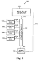
- FIG. 1 illustrates a simplified block diagram of a memory device 100 according to one embodiment of the present invention.
- Memory device 100 includes a write pulse generator 102, a distribution circuit 104, memory cells 106a, 106b, 106c, and 106d, and a sense circuit 108.
- memory cells 106a-106d are phase change memory cells that beneficially employ an amorphous- crystalline phase transition of memory material within the cell for storing data in the memory.
- Write pulse generator 102 is electrically coupled to distribution circuit 104 through signal path 110.
- Distribution circuit 104 is electrically coupled to memory cells 106a-106d through signal paths 112a-112d, respectively, and to sense circuit 108 through signal path 114.
- Write pulse generator 102 is electrically coupled to sense circuit 108 through a signal path 116.
- Each of the memory cells 106a-106d can be programmed into a memory state associated with a particular resistance value, and the resistance value is controlled using a suitable electrical write strategy.
- electrically coupled is not meant to mean that the elements must be directly coupled together, and intervening elements may be provided between the “electrically coupled” elements.
- phase change materials exhibit more than one crystalline phase.
- a low temperature crystalline state may have a lower electrical resistance than the amorphous state
- a high-temperature crystalline state may have an electrical resistance that is lower than both the lower temperature crystalline state and the amorphous state.
- the transition of the phase change material into the higher temperature crystalline state is not generally desirable because a large current is required to switch the phase change material from the high temperature crystalline state back to the amorphous state.
- each phase change memory cell 106a-106d includes phase change material providing a data storage location.
- the active region for the phase change memory cell is where the phase change material transitions between the crystalline state and the amorphous state for storing one bit, 1.5 bits, two bits, or several bits of data.
- write pulse generator 102 generates current or voltage pulses that are controllably directed to memory cells 106a-106d via distribution circuit 104.
- distribution circuit 104 includes a plurality of transistors that controllably direct current or voltage pulses to the memory cells.
- memory cells 106a-106d include a phase change material that can be changed from an amorphous state to a crystalline state, or from a crystalline state to an amorphous state, under influence of a temperature change.
- the degree of crystallinity defines at least two memory states useful for storing data within memory device 100.
- the memory state(s) can be assigned to the bit values, such as bit values "0" and "1.”
- the bit states of memory cells 106a-106d differ significantly in their electrical resistivity. In the amorphous state, a phase change material exhibits significantly higher resistivity than in the crystalline state. In this manner, sense amplifier 108 reads the cell resistance such that the bit value assigned to a particular memory cell 106a-106d is determined.
- write pulse generator 102 To program one of the memory cells 106a-106d within memory device 100, write pulse generator 102 generates a current or voltage pulse for heating the phase change material in the target memory cell. In one embodiment, write pulse generator 102 generates an appropriate current or voltage pulse, which is fed into distribution circuit 104 and distributed to the appropriate target memory cell 106a-106d. The current or voltage pulse amplitude and duration is controlled depending on whether the memory cell is being set or reset. Generally, a "set” operation of a memory cell heats the phase change material of the target memory cell above its crystallization temperature (but below its melting temperature) long enough to achieve the crystalline state. Generally, a “reset” operation of a memory cell heats the phase change material of the target memory cell above its melting temperature, and then quickly quenches/cools the material, thereby achieving the amorphous state.
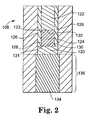
- FIG. 2 illustrates a cross-sectional view of a memory cell 106 according to one embodiment of the present invention.
- memory cell 106 includes a dedicated electrode 120, a second electrode 122, a layer 124 of phase change material extending between dedicated electrode 120 and second electrode 122, and a sidewall 126 contacting the second electrode 122 and a sidewall 128 of layer 124 of phase change material.
- layer 124 of phase change material extends from a first contact 130 with the dedicated electrode 120 to a second contact 132 with second electrode 122.
- first contact 130 is a lower contact and second contact 132 is an upper contact 132, although other orientations are acceptable.
- dedicated electrode 120 contacts an electrode plug 134 within a portion of a pre-processed wafer 136 and provides improved interface control for subsequent processing.
- dedicated electrode 120 is optional, and layer 124 of phase change material contacts electrode plug 134 directly.
- Dedicated electrode 120 and second electrode 122 include titanium nitride (TiN), tantalum nitride (TaN), tungsten (W), or other suitable electrode material.
- electrode plug 134 is a TiN plug, a tungsten plug, a copper plug, or a plug of other suitable electrode material.
- Layer 124 of phase change material can be fabricated from a variety of materials in accordance with the present invention.
- layer 124 of phase change material includes chalcogenide alloys having one or more elements from Group VI of the periodic table, such as Tellurium and/or Selenium and/or Sulfur, and their alloys.
- layer 124 of phase change material is chalcogen-free, i.e., a phase change material that does not contain Tellurium, Selenium, or Sulfur, or alloys of Tellurium, Selenium, or Sulfur.
- Suitable materials for layer 124 of phase change material include, for example, GeSbTe, SbTe, GeTe, AgInSbTe, GeSb, GaSb, InSb, GeGaInSb.
- layer 124 includes a suitable material including one or more of the elements Ge, Sb, Te, Ga, As, In, Se, and S.
- layer 124 of phase change material may be selectively doped with nitrogen, oxygen, silicon, or other suitable materials.
- Layer 124 defines at least one dimension related to film thickness, where a thickness dimension of layer 124 is less than about 100 nanometers (nm).
- spacer layer 124 is a phase change material as described above and has a dimension that is between about 100 nanometers and 5 nanometers.
- layer 124 of phase change material includes a first stack 131 of phase change material in contact with a second stack 133 of phase change material.
- first stack 131 of phase change material is different in composition relative to second stack 133 of phase change material.
- sidewall spacer 126 includes material having a lower electrical conductivity than phase change material in layer 124 in its crystalline state.
- sidewall spacer 126 is an insulation dielectric and includes, for example, silicon dioxide (SiO 2 ) SiOCH, or other suitable low-k materials.
- sidewall spacer 126 is a suitable insulation material that defines an etch rate for plasma etchants that is lower than an etch rate for layer 124 of phase change material.
- low etch rate sidewall spacer 126 protects and improves homogeneity of layer 124. Improved homogeneity of layer 124 relates to improved structural integrity and improved, uniform electrical characteristics of layer 124.
- sidewall spacer 126 is a multi-layer structure including at least one stress layer and one insulation layer.
- stress layer of sidewall spacer 126 includes a densified layer of silicon nitride, such as Si 3 N 4 , or other suitable stress layer materials.
- Figures 3A-10 illustrate various embodiments of sidewall spacer 126 employed to minimize or limit uncontrolled over-etching of layer 124 during, for example, bottom electrode 120 etching.
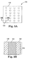
- FIG. 3A illustrates a top view of a pre-processed wafer 136 according to one embodiment of the present invention.
- Pre-processed wafer 136 includes electrode plugs 134 disposed in a dielectric field 138.
- Dielectric field 138 is, in general, an insulating field and can include an oxide field, a nitride field, or other dielectric material having suitable thermal etch and electrical characteristics. With this in mind, dielectric field 138 is also referred to as an insulator 138.
- Insulator 138 can include silicon dioxide, fluorinated silica glass (FSG), or other suitable dielectric materials.
- FIG. 3B illustrates a cross-sectional view of a portion of pre-processed wafer 136 according to one embodiment of the present invention. Electrode plug 134 is laterally surrounded by insulator 138 and prepared for subsequent processing.
- FIG. 4 illustrates a cross-sectional view of a memory cell stack 140 according to one embodiment of the present invention.
- Memory cell stack 140 is disposed on pre-processed wafer 136 and includes a dedicated electrode layer 120a, a second electrode layer 122a, and a layer 124a of phase change material extending between dedicated electrode layer 120a and second electrode layer 122a.
- memory cell stack 140 includes hard mask layer 142 deposited onto second electrode layer 122a, and a photo resist layer 144 deposited on hard mask layer 142.
- hard mask 142 is a stop etch layer including silicon nitride, such as SiN, or SiON, or other suitable stop etch materials.
- Dedicated electrode layer 120a can be deposited using chemical vapor deposition (CVD), atomic layer deposition (ALD), metal organic chemical vapor deposition (MOCVD), plasma vapor deposition (PVD), jet vapor deposition (JVD), or other suitable depositions techniques.
- CVD chemical vapor deposition
- ALD atomic layer deposition
- MOCVD metal organic chemical vapor deposition
- PVD plasma vapor deposition
- JVD jet vapor deposition
- Layer 124a and second electrode layer 122a are likewise deposited employing suitable deposition techniques.
- layer 124 of phase change material and second electrode layer 122a are deposited using one of CVD, ALD, MOCVD, PVD, JVD, or other suitable deposition techniques.
- photo resist 144 is spin coated onto hard mask 142, and the photo resist is employed to pattern hard mask 142.
- Photo resist layer 144 can include photo resist materials useful in, for example, optical lithography.
- a size of the photoresist is reduced after lithography by reactive ion trimming.
- hard mask 142 is a silicon nitride or a silicon oxynitride deposited by a suitable deposition technique, such as CVD, ALD, MOCVD, PVD, and/or JVD.
- resist 144 is trimmed, hard mask 142 is opened, resist 144 is stripped, and memory cell stack 140 is etched.
- Figure 5 illustrates a cross-sectional view of memory cell stack 140 ( Figure 4) after an etch and strip process according to one embodiment of the present invention.
- Memory cell stack 140 has been vertically etched down to dedicated electrode layer 120a, and a width of etched memory cell stack 140 is approximately the width of photo resist layer 144 after trimming ( Figure 4).
- photo resist layer 144 is stripped to expose remaining hard mask 142.
- photoresist layer 144 is already stripped after the hard mask 142 is opened.
- Figure 6 illustrates a cross-sectional view of a sidewall spacer layer 126a deposited over the etched memory cell stack shown in Figure 5 according to one embodiment of the present invention.
- Sidewall spacer layer 126a defines a lateral spacer 127 in contact with lateral portions of dedicated electrode layer 120a, and a remaining vertical spacer in contact with vertical portions of layer 124 of phase change material and second electrode 122.
- sidewall spacer layer 126a includes one of SiN, SiON, SiO2, or a low-k dielectric material and is deposited using CVD, ALD, MOCVD, PVD, JVP, or other suitable deposition techniques.
- Figure 7 illustrates a cross-sectional view of a vertical sidewall spacer 126 according to one embodiment of the present invention.
- sidewall spacer layer 126a ( Figure 6) is anisotropically etched to remove lateral spacer 127 ( Figure 6) of spacer layer 126a from dedicated electrode layer 120a and hard mask 144 ( Figure 6).
- lateral spacer 127 of sidewall spacer layer 126a is removed by a directed top down etch to remove horizontal portions (i.e., lateral portions, or lateral spacer 127) of sidewall spacer layer 126a.
- a vertical sidewall spacer 126 remains in contact with layer 124 of phase change material and second electrode 122.
- sidewall spacer 126 is a sidewall protection spacer configured to protect layer 124 of phase change material during subsequent etching of a bottom electrode, for example dedicated electrode layer 120a, from harsh halogen etch chemistry. It is desired that sidewall spacer 126 have an etch rate that is lower than an etch rate for layer 124 for the given etching chemistry, such that during etching of bottom electrode layer 120a, over-etching of layer 124 is minimized or reduced.
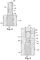
- FIG 8 illustrates a cross-sectional view of dedicated electrode 120 according to one embodiment of the present invention.
- dedicated electrode layer 120a ( Figure 7) is separation etched down to a top portion of pre-processed wafer 136 ( Figure 2) to define a patterned bottom electrode.
- the separation etch of dedicated electrode layer 120a is a self-aligned bottom electrode separation etch employing a chlorine plasma.
- One aspect of the invention provides sidewall spacer 126 that prevents further etching or degradation of layer 124 of phase change material during the bottom electrode separation etch.
- Figure 9 illustrates a cross-sectional view of a dielectric material 150 disposed around sidewall spacer 126 according to one embodiment of the present invention.
- an interlayer dielectric 150 is deposited to surround portions of dedicated electrode 120, sidewall spacer 126, and hard mask 144.
- interlayer 150 is insulation material similar to insulator 138.
- electrodes 120, 122 and layer 124 of phase change material are laterally completely enclosed by insulation material 150.
- Figure 10 illustrates a cross-sectional view of memory cell 106 according to one embodiment of the present invention.
- insulation material 150 ( Figure 9) is planarized using a chemical mechanical polishing (CMP), or other suitable planarizing techniques, to define memory cell 106, which is thereafter configured for subsequent further wiring/processing in accordance with aspects of the present invention.
- CMP chemical mechanical polishing
- Memory cell 106 includes layer 124 of phase change material extending between dedicated electrode 120 and second electrode 122, where layer 124 of phase change material has improved structural homogeneity. For example, layer 124 of phase change material is protected by sidewall spacer 126 from deleterious or undesired over etching during bottom electrode separation processing.
- a non-uniform top electrode layer for example electrode 122
- a non-uniform thickness that makes an exact end pointing of a pillar etch processing difficult. Consequently, certain amounts of over etching can occur and affect components of memory cell 106. Over etching can lead to uncontrolled undercutting of layer 124, that in turn leads to sputter redeposition of undesired (i.e., later and additional) sidewall coatings on pillar cell 106.
- Embodiments of this invention provide sidewall spacer 126 that protects against over etching of sidewall portions of layer 124 of phase change material.
- sidewall spacer 126 has an etch rate that is lower than an etch rate of layer 124, such that sidewall spacer 126 protects against over etching of sidewall portions of layer 124 of phase change material.
- Figure 11A illustrates a cross-sectional view of another memory cell stack 160 according to one embodiment of the present invention.
- memory cell stack 160 is deposited on top of pre-processed wafer 136.
- electrode layer 120a ( Figure 4) is optional and not included as part of memory cell stack 160.
- memory cell stack 160 includes layer 124a of phase change material deposited directly onto electrode plug 134, second electrode layer 122a disposed on top of layer 124a, hard mask layer 142 deposited on second electrode layer 122a, and photo resist 144 deposited onto hard mask layer 142.
- photo resist layer 144 and hard mask 142 are similar to the photo resist and hard mask materials described in Figure 4 above.
- Figure 11B illustrates a cross-sectional view of a memory cell 166 fabricated from memory cell stack 160 according to one embodiment of the present invention.
- layer 124 of phase change material extends between electrode plug 134 and second electrode 122.
- a sidewall spacer 176 contacts a sidewall of layer 124 of phase change material and second electrode 122.
- An insulator material 180 is provided to insulate portions of memory cell 166.
- Figures 12-25 provide various other embodiments of a memory cell that includes a sidewall spacer configured to protect a layer of phase change material during etching, and in particular, to protect layer of phase change material from over etching during bottom electrode separation etching. Aspects of the invention provide for a sidewall spacer that additionally covers a layer of phase change material to further insulate hot spots in the phase change material during memory set and memory reset. In various embodiments, the sidewall spacer laterally encloses a layer of phase change material, and the sidewall spacer and layer of phase change material, when etched, provide for a wider base in contact with a bottom electrode that improves the structural integrity of the pillar phase change cell and the electrical characteristics of the phase change memory.
- FIG. 12 illustrates a cross-sectional view of a memory cell 206 according to another embodiment of the present invention.
- memory cell 206 includes a first electrode 220, a second electrode 222, a layer 224 of phase change material extending from first electrode 220 to second electrode 222, and a sidewall spacer 226 in contact with second electrode 222 and a sidewall 228 of layer 224.
- layer 224 of phase change material extends from a lower contact 230 of first electrode 220 to an upper contact 232 of second electrode 222.
- layer 224 of phase change material includes a base 225 and a pillar 227 extending from base 225. As illustrated in Figure 12, base 225 contacts first electrode 220 along lower contact 230, and pillar 227 contacts second electrode 222 along upper contact 232.
- base 225 is laterally disposed on first electrode 220, and pillar 227 is narrower than base 225 such that pillar 227 contacts only a portion of base 225. In one embodiment, pillar 227 extends orthogonally from base 225, although other orientations of pillar 227 relative to base 225 are acceptable.
- first electrode 220 contacts an electrode plug 234 of a pre-processed wafer 236.
- electrode plug 234 and pre-processed wafer 236 are substantially similar to electrode plug 134 and pre-processed wafer 136 illustrated in Figures 3A and 3B.
- Figure 13 illustrates a cross-sectional view of a memory cell stack 240 disposed on a pre-processed wafer 236 according to one embodiment of the present invention.
- Pre-processed wafer 236 includes a plurality of electrode plugs 234 disposed in an insulation field 238. It is to be understood that although Figure 13 illustrates one electrode plug 234, in general a pre-processed wafer such as wafer 236 will include many electrode plugs disposed in an insulation field (for example, substantially as shown in Figures 3A and 3B).
- Memory cell stack 240 includes first electrode layer 220a, second electrode layer 222a, a layer 224a of phase change material extending between first electrode layer 220a and second electrode layer 222a, a hard mask 242 deposited onto second electrode layer 222a, and a photo resist layer 244 contacting hard mask 242.
- photo resist layer 244 and hard mask 242 are similar to the photo resist and hard mask materials described in Figure 4 above.
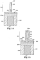
- Figure 14 illustrates a cross-sectional view of a pillar stack 243 according to one embodiment of the present invention.
- Memory cell stack 240 ( Figure 13) has been etched to form storage location pillars, and the main pillar etch has been terminated within the layer 224 of phase change material such that layer 224 defines a base 225, and a pillar 227 extending from base 225.
- pillar stack 243 includes a pillar 227 portion of layer 224 of phase change material, second electrode 222, and a remaining portion of hard mask 242 on second electrode 222.
- photo resist 244 is employed to etch pillar 227. Photo resist 244 is then stripped to expose pillar stack 243. Since main pillar etch has been terminated within base 225, a remaining portion of base 225 is provided that is wider than photo resist 244. In this regard, base 225 improves the structural integrity of pillar 227 and second electrode 222.
- Figure 15 illustrates a cross-sectional view of a sidewall spacer layer 226a deposited onto portions of pillar stack 243 according to one embodiment of the present invention.
- Sidewall spacer layer 226a is conformally deposited onto base 225 and extends in contact along a sidewall 228 of layer 224 of phase change material.
- sidewall spacer layer 226a is a dielectric that is conformally deposited over pillar stack 243 in a CVD process. Other suitable deposition processes are also acceptable.
- sidewall spacer layer 226a contacts sidewall 228 of layer 224 of phase change material adjacent to upper contact 232 of second electrode 222.
- sidewall spacer layer 226a is a multilayer structure that includes at least one stress layer, where the stress layer is configured to suppress a transition in the layer 224 of phase change material to a high temperature crystalline state.
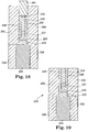
- Figure 16 illustrates a cross-sectional view of a sidewall spacer 226 according to one embodiment of the present invention.
- Pillar stack 243 Figure 15
- Pillar stack 243 Figure 15
- horizontal portions of sidewall spacer layer 226a Figure 15
- sidewall spacer 226 surrounds pillar 227 and extends from base 225 to hard mask/stop etch 242.
- Figure 17 illustrates a cross-sectional view of patterned electrode 220 according to one embodiment of the present invention.
- electrode layer 220a ( Figure 16) is separation etched to define patterned bottom electrode 220.
- the separation etch of electrode layer 220a is a self-aligned bottom electrode separation etch employing a chlorine plasma.
- One aspect of the invention provides sidewall spacer 226 that prevents further etching or degradation of pillar 227 material during the bottom electrode separation etch.
- Figure 18 illustrates a cross-sectional view of an interlayer dielectric layer 250 according to one embodiment of the present invention.
- interlayer 250 is deposited in a suitable deposition process to laterally and completely surround electrodes 220, 222 and sidewall spacer 226.
- interlayer 250 is insulation material similar to insulator 238.
- Figure 19 illustrates a cross-sectional view of memory cell 206 according to one embodiment of the present invention.
- interlayer 250 ( Figure 18) is planarized using a chemical mechanical polishing (CMP), or other suitable planarizing techniques, to define memory cell 206, which is thereafter configured for subsequent further wiring/processing in accordance with aspects of the present invention.
- CMP chemical mechanical polishing
- Figure 20A illustrates a memory cell stack 260 according to another embodiment of the present invention.
- Memory cell stack 260 includes layer 224a of phase change material, second electrode layer 222a, a hard mask/stop etch layer 242 over second electrode layer 222a, and a photo resist 244 masking over hard mask/stop etch layer 242.
- first electrode layer 220a ( Figure 13) is an optional layer that is not provided.
- layer 224a of phase change material is directly deposited onto electrode plug 234 of pre-processed wafer 236.
- Figure 20B illustrates a cross-sectional view of a memory cell 266 according to one embodiment of the present invention.
- Memory cell 266 after processing memory cell stack 260 ( Figure 20A) in processes substantially similar to those illustrated in Figures 12-19, provides layer 224 of phase change material in contact with electrode plug 234, and second electrode 222 in contact with layer 224 of phase change material.
- Memory cell 266 includes insulator 280 that completely and laterally surrounds sidewall spacer 276.
- layer 224 of phase change material includes base 225 in contact with electrode plug 234, and pillar 227 in contact with second electrode 222.
- a sidewall spacer 226 is provided and extends between a top portion of second electrode 222 and base 225 of layer 224 of phase change material. Sidewall spacer 276 contacts second electrode 222 and a sidewall 228 of layer 224 of phase change material adjacent to an upper contact with second electrode 222.
- FIG. 21 illustrates a cross-sectional view of a memory cell 306 according to another embodiment of the present invention.
- memory cell 306 includes a first electrode 320, an etch stop layer 321 in contact with first electrode 320, a second electrode 322, a layer 324 of phase change material extending from etch stop layer 321 to second electrode 322, and a sidewall spacer 326 in contact with second electrode 322 and a sidewall 328 of layer 324.
- first electrode 320 contacts an electrode plug 234 of a pre-processed wafer 236.
- electrode plug 234 and pre-processed wafer 236 are substantially similar to electrode plug 134 and pre-processed wafer 136 illustrated in Figures 3A and 3B.
- Figure 22 illustrates a cross-sectional view of a memory cell stack 340 disposed on a pre-processed wafer 236 according to one embodiment of the present invention.
- Pre-processed wafer 236 includes a plurality of electrode plugs 234 disposed in an insulation field 238. It is to be understood that although Figure 22 illustrates one electrode plug 234, in general a pre-processed wafer such as wafer 236 will include many electrode plugs disposed in an insulation field (for example, substantially as shown in Figures 3A and 3B).
- Memory cell stack 340 includes first electrode layer 320a, etch stop layer 321a, second electrode layer 322a, a layer 324a of phase change material extending between etch stop layer 321a and second electrode layer 322a, a hard mask 342 deposited onto second electrode layer 322a, and a photo resist layer 344 contacting hard mask 342.
- photo resist layer 344 and hard mask 342 are similar to the photo resist and hard mask materials described in Figure 4 above.
- Figure 23 illustrates a cross-sectional view of a pillar stack 343 according to one embodiment of the present invention.
- Memory cell stack 340 ( Figure 22) has been etched to form a storage location pillar, and the pillar etch has been terminated at etch stop layer 321 a to define a column of phase change material 324 extending from etch stop layer 321 a.
- pillar stack 343 includes a pillar of layer 324 of phase change material, second electrode 322, and a remaining portion of hard mask 342 on second electrode 322.
- photo resist 344 is employed in etching pillar 324 lithographically, and then photo resist 344 is subsequently stripped after pillar stack 343 is formed.
- pillar etch is terminated at etch stop layer 321a, and etch stop layer 321 a provides a relatively wider base for pillar stack 343 that, in effect, improves the structural integrity of pillar 224 and second electrode 222.
- Figure 24 illustrates a cross-sectional view of a sidewall spacer layer 326a deposited onto portions of pillar stack 343 according to one embodiment of the present invention.
- Sidewall spacer layer 326a is conformally deposited onto etch stop layer 321 and along a sidewall 228 of layer 324 of phase change material.
- sidewall spacer layer 326a is a dielectric that is conformally deposited over pillar stack 343 in a CVD process. Other suitable deposition processes are also acceptable.
- Sidewall spacer layer 326a protects phase change layer 324 during subsequent etching of bottom electrode layer 320a (and etch stop layer 321a).
- Figure 25 illustrates a cross-sectional view of a memory cell 306 according to the present invention.
- Pillar stack 343 ( Figure 24) and sidewall spacer layer 326a have been anisotropically and separation etched in a manner similar to that described above in Figures 16 and 17, and an interlayer dielectric 350 has been deposited in a suitable deposition process to laterally and completely surround electrodes 320, 322 and sidewall spacer 326, in a manner similar to that described above in Figure 18.
- aspects of the invention provide a sidewall spacer that protects and improves homogeneity of a phase change material layer from over etching during, for example, a bottom electrode separation etch.
- Improved homogeneity of phase change material layer relates to improved structural integrity and improved, uniform electrical characteristics of phase change material layer, all of which contributes to a low power phase change memory cell structure.
Landscapes
- Engineering & Computer Science (AREA)
- Manufacturing & Machinery (AREA)
- Semiconductor Memories (AREA)
Applications Claiming Priority (1)
| Application Number | Priority Date | Filing Date | Title |
|---|---|---|---|
| US11/406,766 US8896045B2 (en) | 2006-04-19 | 2006-04-19 | Integrated circuit including sidewall spacer |
Publications (2)
| Publication Number | Publication Date |
|---|---|
| EP1848048A2 true EP1848048A2 (de) | 2007-10-24 |
| EP1848048A3 EP1848048A3 (de) | 2008-01-02 |
Family
ID=38293002
Family Applications (1)
| Application Number | Title | Priority Date | Filing Date |
|---|---|---|---|
| EP07007522A Withdrawn EP1848048A3 (de) | 2006-04-19 | 2007-04-12 | Speicherzelle mit Seitenwand-Abstandshalter für verbesserte Homogenität |
Country Status (4)
| Country | Link |
|---|---|
| US (1) | US8896045B2 (de) |
| EP (1) | EP1848048A3 (de) |
| JP (1) | JP2007288201A (de) |
| KR (1) | KR100880667B1 (de) |
Cited By (5)
| Publication number | Priority date | Publication date | Assignee | Title |
|---|---|---|---|---|
| WO2010008938A1 (en) * | 2008-07-15 | 2010-01-21 | Sandisk 3D, Llc | Electronic devices including carbon-based films having sidewall liners, and methods of forming such devices |
| WO2010076837A1 (en) * | 2008-12-31 | 2010-07-08 | Michele Magistretti | Avoiding degradation of chalcogenide material during definition of multilayer stack structure |
| KR101107481B1 (ko) * | 2007-11-14 | 2012-01-19 | 가부시끼가이샤 도시바 | 불휘발성 반도체 기억 장치 |
| US20240074334A1 (en) * | 2022-08-25 | 2024-02-29 | Taiwan Semiconductor Manufacturing Company, Ltd. | Phase-change memory device and method for fabricating the same |
| JP2024529708A (ja) * | 2021-08-20 | 2024-08-08 | インターナショナル・ビジネス・マシーンズ・コーポレーション | 相変化メモリセルスペーサ |
Families Citing this family (44)
| Publication number | Priority date | Publication date | Assignee | Title |
|---|---|---|---|---|
| KR100945790B1 (ko) | 2008-02-15 | 2010-03-08 | 주식회사 하이닉스반도체 | 상변화 메모리 소자 및 그 제조 방법 |
| US8084842B2 (en) * | 2008-03-25 | 2011-12-27 | Macronix International Co., Ltd. | Thermally stabilized electrode structure |
| US8445385B2 (en) * | 2008-04-11 | 2013-05-21 | Sandisk 3D Llc | Methods for etching carbon nano-tube films for use in non-volatile memories |
| US8415651B2 (en) | 2008-06-12 | 2013-04-09 | Macronix International Co., Ltd. | Phase change memory cell having top and bottom sidewall contacts |
| US7888165B2 (en) * | 2008-08-14 | 2011-02-15 | Micron Technology, Inc. | Methods of forming a phase change material |
| US8124950B2 (en) * | 2008-08-26 | 2012-02-28 | International Business Machines Corporation | Concentric phase change memory element |
| US7834342B2 (en) * | 2008-09-04 | 2010-11-16 | Micron Technology, Inc. | Phase change material and methods of forming the phase change material |
| US20100078621A1 (en) * | 2008-10-01 | 2010-04-01 | Breitwisch Mathew J | Method to reduce reset current of pcm using stress liner layers |
| US8829646B2 (en) * | 2009-04-27 | 2014-09-09 | Macronix International Co., Ltd. | Integrated circuit 3D memory array and manufacturing method |
| US8031518B2 (en) * | 2009-06-08 | 2011-10-04 | Micron Technology, Inc. | Methods, structures, and devices for reducing operational energy in phase change memory |
| US8283650B2 (en) | 2009-08-28 | 2012-10-09 | International Business Machines Corporation | Flat lower bottom electrode for phase change memory cell |
| US8283202B2 (en) | 2009-08-28 | 2012-10-09 | International Business Machines Corporation | Single mask adder phase change memory element |
| US8012790B2 (en) * | 2009-08-28 | 2011-09-06 | International Business Machines Corporation | Chemical mechanical polishing stop layer for fully amorphous phase change memory pore cell |
| US8129268B2 (en) | 2009-11-16 | 2012-03-06 | International Business Machines Corporation | Self-aligned lower bottom electrode |
| US8233317B2 (en) * | 2009-11-16 | 2012-07-31 | International Business Machines Corporation | Phase change memory device suitable for high temperature operation |
| US7943420B1 (en) * | 2009-11-25 | 2011-05-17 | International Business Machines Corporation | Single mask adder phase change memory element |
| US8431492B2 (en) * | 2010-02-02 | 2013-04-30 | Sandisk 3D Llc | Memory cell that includes a sidewall collar for pillar isolation and methods of forming the same |
| US8198160B2 (en) | 2010-04-19 | 2012-06-12 | Jun Liu | Vertical transistor phase change memory |
| US9082954B2 (en) | 2010-09-24 | 2015-07-14 | Macronix International Co., Ltd. | PCRAM with current flowing laterally relative to axis defined by electrodes |
| JP5295465B2 (ja) * | 2011-02-23 | 2013-09-18 | パナソニック株式会社 | 不揮発性記憶素子及びその製造方法 |
| US8497182B2 (en) | 2011-04-19 | 2013-07-30 | Macronix International Co., Ltd. | Sidewall thin film electrode with self-aligned top electrode and programmable resistance memory |
| JP5984942B2 (ja) * | 2011-09-22 | 2016-09-06 | インテル・コーポレーション | メモリ装置を製造する方法および装置 |
| US8987700B2 (en) | 2011-12-02 | 2015-03-24 | Macronix International Co., Ltd. | Thermally confined electrode for programmable resistance memory |
| US8981330B2 (en) | 2012-07-16 | 2015-03-17 | Macronix International Co., Ltd. | Thermally-confined spacer PCM cells |
| CN102881824B (zh) * | 2012-09-25 | 2014-11-26 | 北京大学 | 阻变存储器及其制备方法 |
| US9214351B2 (en) | 2013-03-12 | 2015-12-15 | Macronix International Co., Ltd. | Memory architecture of thin film 3D array |
| US8916414B2 (en) | 2013-03-13 | 2014-12-23 | Macronix International Co., Ltd. | Method for making memory cell by melting phase change material in confined space |
| US9349953B2 (en) | 2013-03-15 | 2016-05-24 | Taiwan Semiconductor Manufacturing Company, Ltd. | Resistance variable memory structure and method of forming the same |
| KR102092772B1 (ko) * | 2013-03-27 | 2020-03-24 | 에스케이하이닉스 주식회사 | 반도체 장치 및 그 제조 방법, 이 반도체 장치를 포함하는 마이크로 프로세서, 프로세서, 시스템, 데이터 저장 시스템 및 메모리 시스템 |
| TWI549229B (zh) | 2014-01-24 | 2016-09-11 | 旺宏電子股份有限公司 | 應用於系統單晶片之記憶體裝置內的多相變化材料 |
| US9559113B2 (en) | 2014-05-01 | 2017-01-31 | Macronix International Co., Ltd. | SSL/GSL gate oxide in 3D vertical channel NAND |
| US9337145B2 (en) | 2014-09-10 | 2016-05-10 | Kabushiki Kaisha Toshiba | Semiconductor memory device |
| US10256406B2 (en) * | 2016-05-16 | 2019-04-09 | Micron Technology, Inc. | Semiconductor structures including liners and related methods |
| WO2018004697A1 (en) * | 2016-07-01 | 2018-01-04 | Intel Corporation | Dual layer metal oxide rram devices and methods of fabrication |
| US10424374B2 (en) | 2017-04-28 | 2019-09-24 | Micron Technology, Inc. | Programming enhancement in self-selecting memory |
| US10541364B2 (en) * | 2018-02-09 | 2020-01-21 | Micron Technology, Inc. | Memory cells with asymmetrical electrode interfaces |
| US10693065B2 (en) | 2018-02-09 | 2020-06-23 | Micron Technology, Inc. | Tapered cell profile and fabrication |
| US10424730B2 (en) | 2018-02-09 | 2019-09-24 | Micron Technology, Inc. | Tapered memory cell profiles |
| US10854813B2 (en) | 2018-02-09 | 2020-12-01 | Micron Technology, Inc. | Dopant-modulated etching for memory devices |
| US11289650B2 (en) * | 2019-03-04 | 2022-03-29 | International Business Machines Corporation | Stacked access device and resistive memory |
| US11121317B2 (en) | 2019-11-14 | 2021-09-14 | Micron Technology, Inc. | Low resistance crosspoint architecture |
| CN114447217B (zh) * | 2020-11-05 | 2025-07-04 | 联华电子股份有限公司 | 半导体结构及其制作方法 |
| US12310262B2 (en) | 2021-11-05 | 2025-05-20 | International Business Machines Corporation | Phase change memory with encapsulated phase change element |
| US12453296B2 (en) | 2022-11-01 | 2025-10-21 | International Business Machines Corporation | Phase-change memory device with conductive cladding |
Family Cites Families (29)
| Publication number | Priority date | Publication date | Assignee | Title |
|---|---|---|---|---|
| US6420725B1 (en) * | 1995-06-07 | 2002-07-16 | Micron Technology, Inc. | Method and apparatus for forming an integrated circuit electrode having a reduced contact area |
| US6545287B2 (en) * | 2001-09-07 | 2003-04-08 | Intel Corporation | Using selective deposition to form phase-change memory cells |
| US6879525B2 (en) | 2001-10-31 | 2005-04-12 | Hewlett-Packard Development Company, L.P. | Feedback write method for programmable memory |
| US6762017B2 (en) * | 2002-01-24 | 2004-07-13 | Robert A. Levine | Control for complete blood count analysis system |
| JP4218527B2 (ja) * | 2002-02-01 | 2009-02-04 | 株式会社日立製作所 | 記憶装置 |
| US7049623B2 (en) * | 2002-12-13 | 2006-05-23 | Ovonyx, Inc. | Vertical elevated pore phase change memory |
| US7485891B2 (en) * | 2003-11-20 | 2009-02-03 | International Business Machines Corporation | Multi-bit phase change memory cell and multi-bit phase change memory including the same, method of forming a multi-bit phase change memory, and method of programming a multi-bit phase change memory |
| US6949435B2 (en) * | 2003-12-08 | 2005-09-27 | Sharp Laboratories Of America, Inc. | Asymmetric-area memory cell |
| KR100546406B1 (ko) * | 2004-04-10 | 2006-01-26 | 삼성전자주식회사 | 상변화 메모리 소자 제조 방법 |
| US7279379B2 (en) * | 2004-04-26 | 2007-10-09 | Micron Technology, Inc. | Methods of forming memory arrays; and methods of forming contacts to bitlines |
| US7482616B2 (en) * | 2004-05-27 | 2009-01-27 | Samsung Electronics Co., Ltd. | Semiconductor devices having phase change memory cells, electronic systems employing the same and methods of fabricating the same |
| KR100675278B1 (ko) * | 2004-05-27 | 2007-01-26 | 삼성전자주식회사 | 산소 장벽막으로 덮여진 상변화 기억 셀들을 갖는 반도체소자들, 이를 채택하는 전자 시스템들 및 이를 제조하는방법들 |
| DE102005025209B4 (de) * | 2004-05-27 | 2011-01-13 | Samsung Electronics Co., Ltd., Suwon | Halbleiterspeicherbauelement, elektronisches System und Verfahren zur Herstellung eines Halbleiterspeicherbauelements |
| KR100615598B1 (ko) * | 2004-07-19 | 2006-08-25 | 삼성전자주식회사 | 평탄화 절연막을 갖는 반도체 장치들 및 그 형성방법들 |
| KR100626381B1 (ko) * | 2004-07-19 | 2006-09-20 | 삼성전자주식회사 | 상변화 기억 소자 및 그 형성 방법 |
| JP4189395B2 (ja) * | 2004-07-28 | 2008-12-03 | シャープ株式会社 | 不揮発性半導体記憶装置及び読み出し方法 |
| KR100653701B1 (ko) * | 2004-08-20 | 2006-12-04 | 삼성전자주식회사 | 반도체 소자의 작은 비아 구조체 형성방법 및 이를 사용한상변화 기억 소자의 제조방법 |
| US7135696B2 (en) * | 2004-09-24 | 2006-11-14 | Intel Corporation | Phase change memory with damascene memory element |
| US8501523B2 (en) * | 2004-10-28 | 2013-08-06 | Micron Technology, Inc. | Depositing titanium silicon nitride films for forming phase change memories |
| US7973301B2 (en) * | 2005-05-20 | 2011-07-05 | Qimonda Ag | Low power phase change memory cell with large read signal |
| US7579615B2 (en) * | 2005-08-09 | 2009-08-25 | Micron Technology, Inc. | Access transistor for memory device |
| US20070082469A1 (en) * | 2005-10-12 | 2007-04-12 | Peters John M | Forming heaters for phase change memories |
| US7601995B2 (en) | 2005-10-27 | 2009-10-13 | Infineon Technologies Ag | Integrated circuit having resistive memory cells |
| US7390691B2 (en) | 2005-10-28 | 2008-06-24 | Intel Corporation | Increasing phase change memory column landing margin |
| US7973384B2 (en) * | 2005-11-02 | 2011-07-05 | Qimonda Ag | Phase change memory cell including multiple phase change material portions |
| US7417245B2 (en) * | 2005-11-02 | 2008-08-26 | Infineon Technologies Ag | Phase change memory having multilayer thermal insulation |
| US7394088B2 (en) * | 2005-11-15 | 2008-07-01 | Macronix International Co., Ltd. | Thermally contained/insulated phase change memory device and method (combined) |
| US7323357B2 (en) * | 2005-11-17 | 2008-01-29 | Qimonda Ag | Method for manufacturing a resistively switching memory cell and memory device based thereon |
| US7599217B2 (en) * | 2005-11-22 | 2009-10-06 | Macronix International Co., Ltd. | Memory cell device and manufacturing method |
-
2006
- 2006-04-19 US US11/406,766 patent/US8896045B2/en not_active Expired - Fee Related
-
2007
- 2007-04-12 EP EP07007522A patent/EP1848048A3/de not_active Withdrawn
- 2007-04-18 KR KR1020070037937A patent/KR100880667B1/ko not_active Expired - Fee Related
- 2007-04-18 JP JP2007109542A patent/JP2007288201A/ja active Pending
Cited By (9)
| Publication number | Priority date | Publication date | Assignee | Title |
|---|---|---|---|---|
| KR101107481B1 (ko) * | 2007-11-14 | 2012-01-19 | 가부시끼가이샤 도시바 | 불휘발성 반도체 기억 장치 |
| KR101107383B1 (ko) | 2007-11-14 | 2012-01-19 | 가부시끼가이샤 도시바 | 불휘발성 반도체 기억 장치 |
| US8575589B2 (en) | 2007-11-14 | 2013-11-05 | Kabushiki Kaisha Toshiba | Nonvolatile semiconductor memory device and method of manufacturing the same |
| WO2010008938A1 (en) * | 2008-07-15 | 2010-01-21 | Sandisk 3D, Llc | Electronic devices including carbon-based films having sidewall liners, and methods of forming such devices |
| US8309407B2 (en) | 2008-07-15 | 2012-11-13 | Sandisk 3D Llc | Electronic devices including carbon-based films having sidewall liners, and methods of forming such devices |
| WO2010076837A1 (en) * | 2008-12-31 | 2010-07-08 | Michele Magistretti | Avoiding degradation of chalcogenide material during definition of multilayer stack structure |
| JP2024529708A (ja) * | 2021-08-20 | 2024-08-08 | インターナショナル・ビジネス・マシーンズ・コーポレーション | 相変化メモリセルスペーサ |
| US20240074334A1 (en) * | 2022-08-25 | 2024-02-29 | Taiwan Semiconductor Manufacturing Company, Ltd. | Phase-change memory device and method for fabricating the same |
| US12317761B2 (en) * | 2022-08-25 | 2025-05-27 | Taiwan Semiconductor Manufacturing Company, Ltd. | Phase-change memory device and method for fabricating the same |
Also Published As
| Publication number | Publication date |
|---|---|
| US8896045B2 (en) | 2014-11-25 |
| JP2007288201A (ja) | 2007-11-01 |
| EP1848048A3 (de) | 2008-01-02 |
| US20070246782A1 (en) | 2007-10-25 |
| KR20070103699A (ko) | 2007-10-24 |
| KR100880667B1 (ko) | 2009-01-30 |
Similar Documents
| Publication | Publication Date | Title |
|---|---|---|
| US8896045B2 (en) | Integrated circuit including sidewall spacer | |
| EP1879232B1 (de) | Stromsparende Phasenwechsel-Speicherzelle mit verschiedenen Phasenwechselmaterialien | |
| US7238994B2 (en) | Thin film plate phase change ram circuit and manufacturing method | |
| US7579613B2 (en) | Thin film fuse phase change RAM and manufacturing method | |
| US7417245B2 (en) | Phase change memory having multilayer thermal insulation | |
| US7514288B2 (en) | Manufacturing methods for thin film fuse phase change ram | |
| US7929340B2 (en) | Phase change memory cell and manufacturing method | |
| US7714312B2 (en) | Phase change memory cell with high read margin at low power operation | |
| US7884343B2 (en) | Phase change memory cell with filled sidewall memory element and method for fabricating the same | |
| US7772581B2 (en) | Memory device having wide area phase change element and small electrode contact area | |
| US7682868B2 (en) | Method for making a keyhole opening during the manufacture of a memory cell | |
| US7879645B2 (en) | Fill-in etching free pore device | |
| US20070045606A1 (en) | Shaping a phase change layer in a phase change memory cell | |
| US20070111429A1 (en) | Method of manufacturing a pipe shaped phase change memory | |
| US7973301B2 (en) | Low power phase change memory cell with large read signal | |
| CN101232075A (zh) | 柱形相变存储单元 | |
| US20080012079A1 (en) | Memory cell having active region sized for low reset current and method of fabricating such memory cells | |
| US12256653B2 (en) | PCM cell with nanoheater surrounded with airgaps |
Legal Events
| Date | Code | Title | Description |
|---|---|---|---|
| PUAI | Public reference made under article 153(3) epc to a published international application that has entered the european phase |
Free format text: ORIGINAL CODE: 0009012 |
|
| AK | Designated contracting states |
Kind code of ref document: A2 Designated state(s): AT BE BG CH CY CZ DE DK EE ES FI FR GB GR HU IE IS IT LI LT LU LV MC MT NL PL PT RO SE SI SK TR |
|
| AX | Request for extension of the european patent |
Extension state: AL BA HR MK YU |
|
| PUAL | Search report despatched |
Free format text: ORIGINAL CODE: 0009013 |
|
| AK | Designated contracting states |
Kind code of ref document: A3 Designated state(s): AT BE BG CH CY CZ DE DK EE ES FI FR GB GR HU IE IS IT LI LT LU LV MC MT NL PL PT RO SE SI SK TR |
|
| AX | Request for extension of the european patent |
Extension state: AL BA HR MK YU |
|
| 17P | Request for examination filed |
Effective date: 20080417 |
|
| 17Q | First examination report despatched |
Effective date: 20080521 |
|
| AKX | Designation fees paid |
Designated state(s): DE FR GB |
|
| 19U | Interruption of proceedings before grant |
Effective date: 20090401 |
|
| 19W | Proceedings resumed before grant after interruption of proceedings |
Effective date: 20091123 |
|
| R17C | First examination report despatched (corrected) |
Effective date: 20080521 |
|
| STAA | Information on the status of an ep patent application or granted ep patent |
Free format text: STATUS: THE APPLICATION IS DEEMED TO BE WITHDRAWN |
|
| 18D | Application deemed to be withdrawn |
Effective date: 20100526 |