JP2007242592A - LIGHT EMITTING DEVICE, LIGHT EMITTING DEVICE MANUFACTURING METHOD, EXPOSURE DEVICE, AND ELECTRONIC DEVICE - Google Patents
LIGHT EMITTING DEVICE, LIGHT EMITTING DEVICE MANUFACTURING METHOD, EXPOSURE DEVICE, AND ELECTRONIC DEVICE Download PDFInfo
- Publication number
- JP2007242592A JP2007242592A JP2006309936A JP2006309936A JP2007242592A JP 2007242592 A JP2007242592 A JP 2007242592A JP 2006309936 A JP2006309936 A JP 2006309936A JP 2006309936 A JP2006309936 A JP 2006309936A JP 2007242592 A JP2007242592 A JP 2007242592A
- Authority
- JP
- Japan
- Prior art keywords
- layer
- pixel electrode
- partition
- hole injection
- light emitting
- Prior art date
- Legal status (The legal status is an assumption and is not a legal conclusion. Google has not performed a legal analysis and makes no representation as to the accuracy of the status listed.)
- Withdrawn
Links
Images


Classifications
-
- H—ELECTRICITY
- H05—ELECTRIC TECHNIQUES NOT OTHERWISE PROVIDED FOR
- H05B—ELECTRIC HEATING; ELECTRIC LIGHT SOURCES NOT OTHERWISE PROVIDED FOR; CIRCUIT ARRANGEMENTS FOR ELECTRIC LIGHT SOURCES, IN GENERAL
- H05B33/00—Electroluminescent light sources
- H05B33/12—Light sources with substantially two-dimensional [2D] radiating surfaces
- H05B33/22—Light sources with substantially two-dimensional [2D] radiating surfaces characterised by the chemical or physical composition or the arrangement of auxiliary dielectric or reflective layers
-
- H—ELECTRICITY
- H10—SEMICONDUCTOR DEVICES; ELECTRIC SOLID-STATE DEVICES NOT OTHERWISE PROVIDED FOR
- H10K—ORGANIC ELECTRIC SOLID-STATE DEVICES
- H10K59/00—Integrated devices, or assemblies of multiple devices, comprising at least one organic light-emitting element covered by group H10K50/00
- H10K59/10—OLED displays
- H10K59/12—Active-matrix OLED [AMOLED] displays
- H10K59/122—Pixel-defining structures or layers, e.g. banks
-
- H—ELECTRICITY
- H05—ELECTRIC TECHNIQUES NOT OTHERWISE PROVIDED FOR
- H05B—ELECTRIC HEATING; ELECTRIC LIGHT SOURCES NOT OTHERWISE PROVIDED FOR; CIRCUIT ARRANGEMENTS FOR ELECTRIC LIGHT SOURCES, IN GENERAL
- H05B33/00—Electroluminescent light sources
- H05B33/10—Apparatus or processes specially adapted to the manufacture of electroluminescent light sources
-
- H—ELECTRICITY
- H05—ELECTRIC TECHNIQUES NOT OTHERWISE PROVIDED FOR
- H05B—ELECTRIC HEATING; ELECTRIC LIGHT SOURCES NOT OTHERWISE PROVIDED FOR; CIRCUIT ARRANGEMENTS FOR ELECTRIC LIGHT SOURCES, IN GENERAL
- H05B33/00—Electroluminescent light sources
- H05B33/12—Light sources with substantially two-dimensional [2D] radiating surfaces
- H05B33/20—Light sources with substantially two-dimensional [2D] radiating surfaces characterised by the chemical or physical composition or the arrangement of the material in which the electroluminescent material is embedded
-
- H—ELECTRICITY
- H10—SEMICONDUCTOR DEVICES; ELECTRIC SOLID-STATE DEVICES NOT OTHERWISE PROVIDED FOR
- H10K—ORGANIC ELECTRIC SOLID-STATE DEVICES
- H10K50/00—Organic light-emitting devices
- H10K50/10—OLEDs or polymer light-emitting diodes [PLED]
- H10K50/17—Carrier injection layers
-
- H—ELECTRICITY
- H10—SEMICONDUCTOR DEVICES; ELECTRIC SOLID-STATE DEVICES NOT OTHERWISE PROVIDED FOR
- H10K—ORGANIC ELECTRIC SOLID-STATE DEVICES
- H10K71/00—Manufacture or treatment specially adapted for the organic devices covered by this subclass
- H10K71/10—Deposition of organic active material
- H10K71/12—Deposition of organic active material using liquid deposition, e.g. spin coating
- H10K71/13—Deposition of organic active material using liquid deposition, e.g. spin coating using printing techniques, e.g. ink-jet printing or screen printing
- H10K71/135—Deposition of organic active material using liquid deposition, e.g. spin coating using printing techniques, e.g. ink-jet printing or screen printing using ink-jet printing
Landscapes
- Physics & Mathematics (AREA)
- Optics & Photonics (AREA)
- Engineering & Computer Science (AREA)
- Microelectronics & Electronic Packaging (AREA)
- Manufacturing & Machinery (AREA)
- Electroluminescent Light Sources (AREA)
Abstract
【課題】クロストークを防止すると共に、輝度ムラを防止した発光装置、発光装置の製造方法、露光装置、及び電子機器を提供する。
【解決手段】本発明は、基板10上に、画素電極111と、画素電極111に対向する陰極12と、画素電極111と陰極12との間に基板10側から積層される正孔注入層110a及び発光層110bとを備える発光装置100であって、隣接する画素電極111,111間には、画素電極111を区画すると共に、画素電極111の周縁部と平面視で重なるようにして正孔注入層形成材料に対し撥液性を有する絶縁層112aが設けられ、絶縁層112aで区画された画素電極111上には正孔注入層110aが設けられ、正孔注入層110aの上面の高さが、絶縁層112aの周縁部上に設けられた絶縁層112aの上面の高さと略同じである。
【選択図】図3Provided are a light emitting device, a method for manufacturing the light emitting device, an exposure device, and an electronic apparatus that prevent crosstalk and brightness unevenness.
In the present invention, a pixel electrode 111, a cathode 12 facing the pixel electrode 111, and a hole injection layer 110a stacked from the substrate 10 side between the pixel electrode 111 and the cathode 12 are formed on a substrate 10. And the light emitting layer 110b, in which a pixel electrode 111 is defined between adjacent pixel electrodes 111 and 111, and a hole is injected so as to overlap with a peripheral portion of the pixel electrode 111 in a plan view. An insulating layer 112a having liquid repellency with respect to the layer forming material is provided. A hole injection layer 110a is provided over the pixel electrode 111 partitioned by the insulating layer 112a, and the height of the upper surface of the hole injection layer 110a is high. The height of the upper surface of the insulating layer 112a provided on the peripheral edge of the insulating layer 112a is substantially the same.
[Selection] Figure 3
Description
本発明は、発光装置、発光装置の製造方法、露光装置、及び電子機器に関する。 The present invention relates to a light emitting device, a method for manufacturing the light emitting device, an exposure apparatus, and an electronic apparatus.
電界発光を利用した有機EL装置は、自己発光のため視認性が高く、薄くて軽い、かつ耐衝撃性に優れるなどの優れた特徴を有することから近年広く注目されている。
この有機EL装置は、スイッチング素子である薄膜トランジスタが形成されたガラス基板等の透明基板上に、ITO、酸化スズ(SnO2)等の透明導電材料からなる陽極と、ポリチオフェン誘導体のドーピング体からなる正孔注入層と、ポリフルオレン等の発光物質からなる発光層と、Ca等の低仕事関数を有する金属材料や金属化合物からなる陰極とを順次積層されて構成されている。
2. Description of the Related Art In recent years, organic EL devices using electroluminescence have attracted widespread attention because they have excellent characteristics such as high visibility due to self-emission, thinness and lightness, and excellent impact resistance.
This organic EL device has a positive electrode made of a transparent conductive material such as ITO or tin oxide (SnO 2 ) and a doped body of a polythiophene derivative on a transparent substrate such as a glass substrate on which a thin film transistor as a switching element is formed. A hole injection layer, a light emitting layer made of a light emitting material such as polyfluorene, and a cathode made of a metal material or metal compound having a low work function such as Ca are sequentially laminated.
これらの有機薄膜の材料として低分子系の材料を用いる場合には、蒸着法による成膜が一般的である。しかし、蒸着法では大面積に均一に成膜するのが困難であった。また高額な真空装置が必要となり、材料使用効率が極めて低い為、低コスト化を図ることが困難であった。
そこで、有機薄膜の材料として高分子材料を用い、スピンコート法、ディップ法、インクジェット法等の液相法により有機薄膜を形成する方法が広く利用されている。以下、(1)スピンコート法、(2)インクジェット法により有機薄膜(正孔注入層及び発光層)を形成する方法について説明する。
When a low molecular weight material is used as the material for these organic thin films, film formation by vapor deposition is common. However, it has been difficult to form a uniform film over a large area by the vapor deposition method. In addition, an expensive vacuum device is required, and the material use efficiency is extremely low, so it is difficult to reduce the cost.
Therefore, a method of forming a thin organic film by a liquid phase method such as a spin coating method, a dip method, and an ink jet method using a polymer material as a material of the organic thin film is widely used. Hereinafter, a method of forming an organic thin film (a hole injection layer and a light emitting layer) by (1) spin coating method and (2) inkjet method will be described.
(1)スピンコート法
スピンコート法により正孔注入層及び発光層を形成する場合、まず、基板上に複数の画素電極を形成した後、画素電極のそれぞれを区画するようにしてSiO2等の材料からなる無機バンク層を形成する。次に、無機バンク層を含む画素電極上の全面に、スピンコート法により正孔注入層を形成した後、この正孔注入層上に発光層を積層する(特許文献1、2参照)。
(1) Spin coating method When a hole injection layer and a light emitting layer are formed by a spin coating method, first, a plurality of pixel electrodes are formed on a substrate, and then each pixel electrode is partitioned so that SiO 2 or the like is formed. An inorganic bank layer made of a material is formed. Next, a hole injection layer is formed on the entire surface of the pixel electrode including the inorganic bank layer by spin coating, and then a light emitting layer is stacked on the hole injection layer (see
(2)インクジェット法
インクジェット法により正孔注入層及び発光層を形成する場合、まず、画素電極を区画するようにして、SiO2、TiO2等の無機材料からなる無機物バンク層を形成する。
そして、この無機物バンク層上にアクリル樹脂、ポリイミド樹脂からなる有機物バンク層を形成する。その後、無機物バンク層の側壁面及び画素電極の電極面に親液処理を施し、有機物バンク層の内壁面及び上面に撥液処理を施す。
このように形成された無機物バンク層及び有機物バンク層に区画された領域内に、正孔注入層を形成し、この正孔注入層上に発光層を積層する。(特許文献2〜5参照)。
Then, an organic bank layer made of acrylic resin or polyimide resin is formed on the inorganic bank layer. Thereafter, the side wall surface of the inorganic bank layer and the electrode surface of the pixel electrode are subjected to lyophilic treatment, and the inner wall surface and upper surface of the organic bank layer are subjected to liquid repellent treatment.
A hole injection layer is formed in the region partitioned into the inorganic bank layer and the organic bank layer thus formed, and a light emitting layer is laminated on the hole injection layer. (See Patent Documents 2 to 5).
しかしながら、上記(1)スピンコート法、(2)インクジェット法により正孔注入層及び発光層を形成する場合には以下の問題があった。 However, when the hole injection layer and the light emitting layer are formed by the above (1) spin coating method and (2) ink jet method, there are the following problems.
(1)スピンコート法の場合、正孔注入層の材料にはPEDOT/PSS(H.CStrack社製バイトロンP)のような抵抗の低い材料が用いられている。ここで、上述したように、正孔注入層は基板全面に形成されるため、正孔注入層の正孔は無機バンク層によって区画された発光領域以外の画素隣接間の正孔注入層にも流れてしまい、いわゆるクロストークが発生してしまう。これにより、画素隣接間の無機バンク層上の正孔注入層が電極と同様に機能する場合があり、発光領域以外の領域で発光し、発光形状輪郭ボケといった品質低下を起こす問題があった。
また、スピンコート法により、正孔注入層等を基板上の全面に形成する場合には、実装部や陰極取り出し領域での剥離除去工程が必要であるという問題があった。
(1) In the case of the spin coat method, a material having a low resistance such as PEDOT / PSS (H. CStrack Vitron®) is used as the material of the hole injection layer. Here, as described above, since the hole injection layer is formed on the entire surface of the substrate, the holes in the hole injection layer are also present in the hole injection layer between adjacent pixels other than the light emitting region partitioned by the inorganic bank layer. The so-called crosstalk occurs. As a result, the hole injection layer on the inorganic bank layer between adjacent pixels may function in the same manner as the electrode, and emits light in a region other than the light emitting region, causing a problem of quality deterioration such as blurring of the light emission shape.
Further, when the hole injection layer or the like is formed on the entire surface of the substrate by the spin coating method, there is a problem that a peeling and removing process is required in the mounting portion and the cathode extraction region.
(2)インクジェット法の場合、有機物バンク層は、フォトリソグラフィー処理による精度を考慮して、無機物バンク層の周縁からある程度の間隔を空けて無機物バンク層上に形成する。従って、無機物バンク層と有機物バンク層との積層部分は段差となる。この無機物バンク層は親液性となっている。そのため、正孔注入層形成材料を無機物バンク層及び有機物バンク層に区画された領域に吐出すると、この段差となる無機物バンク層上にも正孔注入層形成材料が配置される。そして、この正孔注入層上には発光層が形成される。このとき、この段差となる無機物バンク層上に形成される正孔注入層および発光層の膜厚と、各画素領域に形成される正孔注入層および発光層の膜厚とは異なってしまい、バンクで囲まれた領域での発光輝度が異なってしまうという問題があった。 (2) In the case of the ink jet method, the organic bank layer is formed on the inorganic bank layer with a certain distance from the periphery of the inorganic bank layer in consideration of accuracy by photolithography. Therefore, the laminated portion of the inorganic bank layer and the organic bank layer is a step. This inorganic bank layer is lyophilic. Therefore, when the hole injection layer forming material is discharged to a region partitioned into the inorganic bank layer and the organic bank layer, the hole injection layer forming material is also disposed on the inorganic bank layer that forms the step. A light emitting layer is formed on the hole injection layer. At this time, the film thickness of the hole injection layer and the light emitting layer formed on the inorganic bank layer to be the step is different from the film thickness of the hole injection layer and the light emitting layer formed in each pixel region, There has been a problem in that the light emission luminance in the area surrounded by the banks is different.
また、正孔注入層上に発光材料を吐出した後には、乾燥処理を行い、発光材料中の溶剤を蒸発させることにより発光層を形成する。しかし、発光材料の乾燥が開始する点(ピニングポイント)は有機物バンク層の側壁面において毎回同じ位置ではなく、乾燥が開始する位置がばらつく傾向がある。この有機物バンク層の側壁面のピニングポイントのばらつきにより、発光層の中央部と周縁部とで膜厚が異なってしまう場合があり均一な膜厚の発光層を形成することができなかった。これにより、画素領域内の中央部と周縁部とで発光輝度が異なると共に、発光寿命が異なってしまうという問題があった。 In addition, after the light emitting material is discharged onto the hole injection layer, the light emitting layer is formed by performing a drying process and evaporating the solvent in the light emitting material. However, the point at which drying of the light emitting material starts (pinning point) is not the same position every time on the side wall surface of the organic bank layer, and the position at which drying starts tends to vary. Due to variations in the pinning points on the side wall surface of the organic bank layer, the film thickness may differ between the central part and the peripheral part of the light emitting layer, and a light emitting layer with a uniform film thickness cannot be formed. As a result, there is a problem in that the light emission luminance is different between the central portion and the peripheral portion in the pixel region, and the light emission lifetime is different.
本発明は、上記課題に鑑みてなされたものであり、その目的は、クロストークを防止すると共に、各画素の機能層の膜厚を均一かつ平坦に形成し、発光輝度及び発光寿命の均一化を図った発光装置、発光装置の製造方法、露光装置、及び電子機器を提供することにある。 The present invention has been made in view of the above problems, and its purpose is to prevent crosstalk and to form a uniform and flat film thickness of the functional layer of each pixel so as to make the emission luminance and emission life uniform. A light emitting device, a method for manufacturing the light emitting device, an exposure apparatus, and an electronic apparatus are provided.
本発明は、上記課題を解決するために、基板上に、画素電極と、前記画素電極に対向する陰極と、前記画素電極と前記陰極との間に前記基板側から積層される正孔注入層及び発光層とを備える発光装置であって、隣接する前記画素電極間には、前記画素電極を区画すると共に、前記画素電極の周縁部と平面視で重なるようにして正孔注入層材料に対し撥液性を有する絶縁層が設けられ、前記絶縁層に区画された前記画素電極上には前記正孔注入層が設けられ、前記正孔注入層の上面の高さが、前記絶縁層の周縁部上に設けられる前記絶縁層の上面の高さと略同じであることを特徴とする。 In order to solve the above problems, the present invention provides a pixel electrode, a cathode facing the pixel electrode, and a hole injection layer stacked from the substrate side between the pixel electrode and the cathode on the substrate. And a light emitting device, wherein the pixel electrode is partitioned between the adjacent pixel electrodes, and overlaps with a peripheral portion of the pixel electrode in plan view with respect to the hole injection layer material. An insulating layer having liquid repellency is provided, the hole injection layer is provided on the pixel electrode partitioned by the insulating layer, and a height of an upper surface of the hole injection layer is set to a peripheral edge of the insulating layer. It is substantially the same as the height of the upper surface of the insulating layer provided on the part.
この構成によれば、画素電極の周縁部上に設けられる絶縁層は正孔注入層材料に対して撥液性を有するため、絶縁層上に吐出される正孔注入層形成材料ははじかれ、絶縁層に区画された開口部内に流れ込む。また、正孔注入層の上面の高さと絶縁層の上面の高さとは略同じであり、乾燥後、正孔注入層形成材料が絶縁層上に漏れ出さないように制御されている。これは、正孔注入層形成材料の吐出量等の吐出条件を制御することにより可能である。そのため、正孔注入層は、絶縁層によって区画された開口部内の画素電極上にのみ配置され、開口部外側(隣接する画素間)の絶縁層上に配置されることはない。
従って、各画素電極に設けられた正孔注入層のホールが隣接する画素間に流れる、いわゆるクロストークの発生を抑制することができる。よって、電流が隣接する画素間に滲みることによる発光形状輪郭ボケといった表示品質の低下を防止することができる。
According to this configuration, since the insulating layer provided on the peripheral portion of the pixel electrode has liquid repellency with respect to the hole injection layer material, the hole injection layer forming material discharged on the insulating layer is repelled, It flows into the opening defined by the insulating layer. Further, the height of the upper surface of the hole injection layer is substantially the same as the height of the upper surface of the insulating layer, and is controlled so that the hole injection layer forming material does not leak onto the insulating layer after drying. This is possible by controlling the discharge conditions such as the discharge amount of the hole injection layer forming material. Therefore, the hole injection layer is disposed only on the pixel electrode in the opening defined by the insulating layer, and is not disposed on the insulating layer outside the opening (between adjacent pixels).
Therefore, it is possible to suppress the occurrence of so-called crosstalk in which holes in the hole injection layer provided in each pixel electrode flow between adjacent pixels. Therefore, it is possible to prevent deterioration in display quality such as blurring of a light emission shape due to current flowing between adjacent pixels.
また本発明の発光装置は、前記絶縁層及び前記正孔注入層上の全面に前記発光層が設けられたことも好ましい。 In the light emitting device of the present invention, the light emitting layer is preferably provided on the entire surface of the insulating layer and the hole injection layer.
この構成によれば、絶縁層の上面と正孔注入層の上面とは略同じ高さであるため、絶縁層の上面と正孔注入層の上面は連続した平坦面となる。従って、絶縁層及び正孔注入層上に形成される発光層は膜厚の均一かつ平坦な膜となり、輝度ムラのない、均一な発光を得ることができる。 According to this configuration, since the upper surface of the insulating layer and the upper surface of the hole injection layer are substantially the same height, the upper surface of the insulating layer and the upper surface of the hole injection layer are continuous flat surfaces. Therefore, the light emitting layer formed on the insulating layer and the hole injection layer is a flat film with a uniform thickness, and uniform light emission without uneven brightness can be obtained.
本発明は、基板上に、画素電極と、前記画素電極に対向する陰極と、前記画素電極と前記陰極との間に前記基板側から積層される正孔注入層及び発光層とを備える発光装置の製造方法であって、隣接する前記画素電極間に、前記画素電極を区画すると共に、前記画素電極の周縁部と平面視で重なるようにして正孔注入層材料に対し撥液性を有する又は撥液処理が施された絶縁層を形成する絶縁層形成工程と、前記絶縁層に区画された前記画素電極上に、前記正孔注入層の上面の高さが前記絶縁層の上面の高さと略同じとなるようにして前記正孔注入層を形成する正孔注入層形成工程と、前記絶縁層及び前記画素電極上の全面に発光層を形成する発光層形成工程と、を有することを特徴とする。 The present invention provides a light emitting device comprising: a pixel electrode; a cathode facing the pixel electrode; and a hole injection layer and a light emitting layer stacked from the substrate side between the pixel electrode and the cathode on a substrate. The pixel electrode is partitioned between the adjacent pixel electrodes and has a liquid repellency with respect to the hole injection layer material so as to overlap with the peripheral edge of the pixel electrode in plan view, or An insulating layer forming step of forming an insulating layer that has been subjected to a liquid repellent treatment; and the height of the upper surface of the hole injection layer on the pixel electrode partitioned by the insulating layer is the height of the upper surface of the insulating layer. A hole injection layer forming step of forming the hole injection layer so as to be substantially the same; and a light emitting layer forming step of forming a light emitting layer on the entire surface of the insulating layer and the pixel electrode. And
また前記絶縁層形成工程において、前記絶縁層を、窒化ケイ素と炭素とを含む材料を用いて前記絶縁層を形成した後、フッ化系化合物ガスの雰囲気中において前記絶縁層にプラズマ処理を施すことも好ましい。
また前記絶縁層形成工程において、前記絶縁層を酸化ケイ素(SiO2)、窒化ケイ素(SiN)又は酸化チタン(TiO2)により形成した後、前記絶縁層表面にシラン系カップリング処理を施すことも好ましい。
In the insulating layer forming step, the insulating layer is formed using a material containing silicon nitride and carbon, and then the insulating layer is subjected to plasma treatment in an atmosphere of a fluorinated compound gas. Is also preferable.
In the insulating layer forming step, the insulating layer may be formed of silicon oxide (SiO 2 ), silicon nitride (SiN), or titanium oxide (TiO 2 ) and then subjected to silane coupling treatment on the surface of the insulating layer. preferable.
この方法によれば、画素電極の周縁部上に設けられる絶縁層は正孔注入層材料に対して撥液性を有するため、絶縁層上に吐出される正孔注入層形成材料ははじかれ、絶縁層に区画された開口部内に流れ込む。また、正孔注入層の上面と絶縁層の上面の高さとを略同じに形成するため、正孔注入層形成材料が絶縁層上に漏れ出さないようになっている。これは、正孔注入層形成材料の吐出量等の吐出条件を制御することにより可能である。そのため、正孔注入層は、絶縁層によって区画された開口部から溢れることがなく、開口部外側の絶縁層上に配置されることはない。
従って、各画素電極に設けられた正孔注入層のホールが隣接する画素間に流れる、いわゆるクロストークの発生を抑制することができる。よって、電流が隣接する画素間に滲みることによる発光形状輪郭ボケといった表示品質の低下を防止することができる。
According to this method, since the insulating layer provided on the peripheral portion of the pixel electrode has liquid repellency with respect to the hole injection layer material, the hole injection layer forming material discharged on the insulating layer is repelled, It flows into the opening defined by the insulating layer. In addition, since the upper surface of the hole injection layer and the upper surface of the insulating layer are formed to have substantially the same height, the hole injection layer forming material does not leak onto the insulating layer. This is possible by controlling the discharge conditions such as the discharge amount of the hole injection layer forming material. Therefore, the hole injection layer does not overflow from the opening defined by the insulating layer and is not disposed on the insulating layer outside the opening.
Therefore, it is possible to suppress the occurrence of so-called crosstalk in which holes in the hole injection layer provided in each pixel electrode flow between adjacent pixels. Therefore, it is possible to prevent deterioration in display quality such as blurring of a light emission shape due to current flowing between adjacent pixels.
また本発明の発光装置の製造方法は、前記正孔注入層形成工程において、前記正孔注入層を液滴吐出法により形成し、前記発光層形成工程において、前記発光層を液相法により形成することも好ましい In the method for manufacturing a light emitting device of the present invention, the hole injection layer is formed by a droplet discharge method in the hole injection layer forming step, and the light emitting layer is formed by a liquid phase method in the light emitting layer forming step. It is also preferable to
本発明では、絶縁層が撥液性を有する又は撥液処理が施されるため、液滴吐出法を採用した場合でも、絶縁層に区画された開口部の外側に正孔注入層形成材料を漏れ出させることなく、選択的に正孔注入層を形成することができる。従って、液滴吐出法によれば、材料の無駄を抑制することができ、低コストかつ高精度に正孔注入層を形成することができる。
また、本発明によれば、絶縁層及び正孔注入層上は連続した平坦面であるため、簡便なスピンコート法により発光層を形成することができる。これにより、膜厚の均一かつ平坦な発光層を容易に形成することができる。
In the present invention, since the insulating layer has a liquid repellency or is subjected to a liquid repellency treatment, the hole injection layer forming material is provided outside the opening section partitioned by the insulating layer even when the droplet discharge method is adopted. The hole injection layer can be selectively formed without leakage. Therefore, according to the droplet discharge method, waste of material can be suppressed, and the hole injection layer can be formed with low cost and high accuracy.
Further, according to the present invention, since the insulating layer and the hole injection layer are continuous flat surfaces, the light emitting layer can be formed by a simple spin coating method. Thereby, a uniform and flat light-emitting layer can be easily formed.
また本発明の露光装置は、上記発光装置と、回動可能な感光体ドラムとを備え、前記発光装置から出射される光により前記感光体ドラムを露光することを特徴とする。
また本発明の電子機器は、上記発光装置を備えることを特徴とする。
この構成によれば、上述した発光装置を備えるため、輝度ムラのない高品質の露光装置及び電子機器を提供することができる。
The exposure apparatus of the present invention includes the light emitting device and a rotatable photosensitive drum, and exposes the photosensitive drum with light emitted from the light emitting device.
In addition, an electronic apparatus according to the present invention includes the light-emitting device.
According to this configuration, since the above-described light emitting device is provided, it is possible to provide a high-quality exposure apparatus and electronic apparatus without uneven brightness.
本発明は、上記課題を解決するために、基板上に、画素電極と、前記画素電極に対向する陰極と、前記画素電極と前記陰極との間に前記基板側から積層される正孔注入層及び発光層とを備える発光装置であって、隣接する前記画素電極間に、前記画素電極を区画すると共に、前記画素電極の周縁部と平面視で重なるように設けられた前記正孔注入層に対し撥液性を有する第1隔壁と、前記第1隔壁上に前記画素電極を区画するように設けられた第2隔壁とを備え、前記第1隔壁に区画された前記画素電極上には前記正孔注入層が設けられ、前記正孔注入層の上面の高さが、前記画素電極の周縁部上に設けられた前記第1隔壁の上面の高さと略同じであることを特徴とする。 In order to solve the above problems, the present invention provides a pixel electrode, a cathode facing the pixel electrode, and a hole injection layer stacked from the substrate side between the pixel electrode and the cathode on the substrate. And a light emitting device, wherein the pixel electrode is partitioned between the adjacent pixel electrodes, and the hole injection layer is provided so as to overlap with a peripheral portion of the pixel electrode in plan view. A first partition having liquid repellency; and a second partition provided on the first partition so as to partition the pixel electrode, and the pixel electrode partitioned by the first partition has the A hole injection layer is provided, and a height of an upper surface of the hole injection layer is substantially the same as a height of an upper surface of the first partition provided on a peripheral portion of the pixel electrode.
また本発明の発光装置は、前記発光層が前記第1隔壁及び前記正孔注入層上の全面に設けられたことも好ましい。 In the light emitting device of the present invention, the light emitting layer is preferably provided on the entire surface of the first partition and the hole injection layer.
この構成によれば、画素電極の周縁部上に設けられる第1隔壁は正孔注入層に対して撥液性を有するため、第1隔壁上に吐出される正孔注入層形成材料ははじかれ、第1隔壁に区画された開口部内に流れ込む。また、正孔注入層の上面の高さと第1隔壁の上面の高さとは略同じであり、正孔注入層形成材料が第1隔壁上に漏れ出さないように制御されている。これは、正孔注入層形成材料の吐出量等の吐出条件を制御することにより可能である。そのため、正孔注入層が、第1隔壁によって区画された開口部から外側に配置されることはない。このように、第1隔壁の上面と正孔注入層の上面とは略同じ高さであるため、均一かつ平坦な正孔注入層及び発光層を形成することができる。さらに、正孔注入層及び発光層の周縁部と中央部とで膜厚を均一にすることができるため、発光寿命ムラのなく、発光寿命の均一化を図ることができる。 According to this configuration, since the first partition provided on the peripheral edge of the pixel electrode has liquid repellency with respect to the hole injection layer, the hole injection layer forming material discharged on the first partition is repelled. And flows into the opening section defined by the first partition. Further, the height of the upper surface of the hole injection layer is substantially the same as the height of the upper surface of the first partition, and the hole injection layer forming material is controlled so as not to leak onto the first partition. This is possible by controlling the discharge conditions such as the discharge amount of the hole injection layer forming material. Therefore, the hole injection layer is not disposed outside from the opening defined by the first partition. As described above, since the upper surface of the first partition and the upper surface of the hole injection layer are substantially the same height, a uniform and flat hole injection layer and a light emitting layer can be formed. Furthermore, since the film thickness can be made uniform between the peripheral portion and the central portion of the hole injection layer and the light emitting layer, the light emitting lifetime can be made uniform without unevenness of the light emitting lifetime.
本発明は、基板上に、画素電極と、前記画素電極に対向する陰極と、前記画素電極と前記陰極との間に前記基板側から積層される正孔注入層及び発光層とを備える発光装置の製造方法であって、隣接する前記画素電極間に、前記画素電極を区画すると共に、前記画素電極の周縁部と平面視で重なるようにして正孔注入層材料に対し撥液性を有する第1隔壁を形成する第1隔壁形成工程と、前記第1隔壁上に前記画素電極を区画するようにして第2隔壁を形成する第2隔壁形成工程と、前記第1隔壁及び前記第2隔壁に区画された前記画素電極上に、前記正孔注入層の上面の高さが、前記画素電極の周縁部上に設けられた前記第1隔壁の上面の高さと略同じとなるようにして前記正孔注入層を形成する正孔注入層形成工程と、前記第1隔壁及び前記第2隔壁に区画された前記正孔注入層上の全面に発光層を形成する発光層形成工程と、を有することを特徴とする。 The present invention provides a light emitting device comprising: a pixel electrode; a cathode facing the pixel electrode; and a hole injection layer and a light emitting layer stacked from the substrate side between the pixel electrode and the cathode on a substrate. The pixel electrode is partitioned between the adjacent pixel electrodes, and has a liquid repellency with respect to the hole injection layer material so as to overlap with a peripheral portion of the pixel electrode in plan view. A first barrier rib forming step of forming one barrier rib; a second barrier rib forming step of forming a second barrier rib so as to partition the pixel electrode on the first barrier rib; and the first barrier rib and the second barrier rib. On the partitioned pixel electrode, the height of the upper surface of the hole injection layer is substantially the same as the height of the upper surface of the first partition provided on the peripheral edge of the pixel electrode. A hole injection layer forming step of forming a hole injection layer; the first partition; and A light emitting layer forming step of forming a light-emitting layer and the serial sectioned in the second partition in the hole injection on the layer over the entire surface, and having a.
また発光装置の製造方法は、前記第1隔壁形成工程において、窒化ケイ素と炭素とを含む材料を用いて前記第1隔壁を形成した後、フッ化系化合物ガスの雰囲気中において前記第1隔壁にプラズマ処理し、前記第1隔壁に撥液処理を施すことも好ましい。 In the method for manufacturing a light emitting device, in the first partition formation step, the first partition is formed using a material containing silicon nitride and carbon, and then the first partition is formed in an atmosphere of a fluorinated compound gas. It is also preferable to perform plasma treatment and perform a liquid repellent treatment on the first partition.
また発光装置の製造方法は、前記第1隔壁形成工程において、前記第1隔壁を酸化ケイ素、窒化ケイ素、又は酸化チタンにより形成した後、前記第2隔壁形成工程後、シラン系カップリング処理を施し、前記第1隔壁表面に撥液処理を施すことも好ましい。 In the method for manufacturing a light emitting device, in the first partition formation step, the first partition is formed of silicon oxide, silicon nitride, or titanium oxide, and after the second partition formation step, a silane coupling treatment is performed. It is also preferable to perform a liquid repellent treatment on the surface of the first partition wall.
また発光装置の製造方法は、前記第2隔壁形成後、フッ化系化合物ガスの雰囲気中においてプラズマ処理し、前記第2隔壁に撥液処理を施すことも好ましい。 In the method for manufacturing a light emitting device, it is preferable that after the second partition is formed, plasma treatment is performed in an atmosphere of a fluorinated compound gas, and the liquid repellent treatment is performed on the second partition.
この方法によれば、画素電極の周縁部上に設けられる第1隔壁は正孔注入層材料に対して撥液性を有するため、第1隔壁上に吐出される正孔注入層形成材料ははじかれ、第1隔壁に区画された開口部内に流れ込む。また、正孔注入層の上面の高さと第1隔壁の上面の高さとは略同じであり、正孔注入層形成材料が第1隔壁上に漏れ出さないように制御されている。これは、正孔注入層形成材料の吐出量等の吐出条件を制御することにより可能である。そのため、正孔注入層が、第1隔壁によって区画された開口部から外側に配置されることはない。このように、第1隔壁の上面と正孔注入層の上面とは略同じ高さであるため、均一かつ平坦な正孔注入層及び発光層を形成することができる。さらに、正孔注入層及び発光層の周縁部と中央部とで膜厚を均一にすることができるため、発光寿命ムラのなく、発光寿命の均一化を図ることができる。 According to this method, since the first partition provided on the peripheral edge of the pixel electrode has liquid repellency with respect to the hole injection layer material, the hole injection layer forming material ejected on the first partition is repelled. And flows into the opening section defined by the first partition. Further, the height of the upper surface of the hole injection layer is substantially the same as the height of the upper surface of the first partition, and the hole injection layer forming material is controlled so as not to leak onto the first partition. This is possible by controlling the discharge conditions such as the discharge amount of the hole injection layer forming material. Therefore, the hole injection layer is not disposed outside from the opening defined by the first partition. As described above, since the upper surface of the first partition and the upper surface of the hole injection layer are substantially the same height, a uniform and flat hole injection layer and a light emitting layer can be formed. Furthermore, since the film thickness can be made uniform between the peripheral portion and the central portion of the hole injection layer and the light emitting layer, the light emitting lifetime can be made uniform without unevenness of the light emitting lifetime.
また本発明の発光装置の製造方法は、前記正孔注入層形成工程において、前記正孔注入層を液滴吐出法により形成し、前記発光層形成工程において、前記発光層を液滴吐出法により形成することも好ましい。 In the method for manufacturing a light emitting device of the present invention, the hole injection layer is formed by a droplet discharge method in the hole injection layer formation step, and the light emission layer is formed by a droplet discharge method in the light emission layer formation step. It is also preferable to form.
本発明によれば、液滴吐出法により正孔注入層及び発光層を選択的に形成することができる。従って、材料の無駄を抑制することができ、低コストかつ高精度に正孔注入層及び発光層を形成することができる。 According to the present invention, the hole injection layer and the light emitting layer can be selectively formed by a droplet discharge method. Therefore, waste of material can be suppressed, and the hole injection layer and the light emitting layer can be formed with low cost and high accuracy.
本発明は、上記課題を解決するために、基板上に、画素電極と、前記画素電極に対向する陰極と、前記画素電極と前記陰極との間に前記基板側から積層される正孔注入層及び発光層とを備える発光装置であって、隣接する前記画素電極間に、前記画素電極を区画すると共に、前記画素電極の周縁部と平面視で重なるように設けられた第1隔壁と、
前記第1隔壁上に、前記画素電極を区画するように設けられた第2隔壁とを備え、前記第2隔壁の側面には、撥液性を有する第1領域と、前記第1領域よりも撥液性が相対的に低い第2領域とが設けられたことを特徴とする。
In order to solve the above problems, the present invention provides a pixel electrode, a cathode facing the pixel electrode, and a hole injection layer stacked from the substrate side between the pixel electrode and the cathode on the substrate. And a light-emitting device comprising: a light-emitting device, wherein the pixel electrode is partitioned between the adjacent pixel electrodes, and the first partition wall is provided so as to overlap with a peripheral portion of the pixel electrode in plan view;
A second partition provided on the first partition so as to partition the pixel electrode; a first region having liquid repellency on a side surface of the second partition; A second region having a relatively low liquid repellency is provided.
この構成によれば、第2隔壁の側面の第2領域は、第1領域よりも撥液性が相対的に低く、吐出される発光層形成材料が第1領域よりも濡れ易くなっている。そのため、この第2領域は、発光層形成材料の乾燥、析出が開始するピニングポイントとなる。従って、第2隔壁の第2領域の位置を調節することにより、乾燥、析出を開始するピニングポイントを制御(固定)することが可能となる。これにより、発光層形成材料の吐出量等を制御することで、乾燥後の膜厚を制御することができ、より均一かつ平坦な発光層を形成することができる。
ここで、ピニング現象について説明する。
一般に基板上に配置された液滴は周縁部(エッジ)において乾燥の進行が速い。従って、液滴が溶媒を含む場合、この液滴の乾燥過程においては、液滴の周縁部において溶質等の濃度がまず飽和濃度に達し、析出し始める。一方、液滴内部には、液滴周縁部で蒸発により失われた液体を補給するため、液滴中央部から周縁部に向かう液体の流れが生じる。この結果、液滴中央部の溶媒は、その流れに従って周縁部に運ばれ、液滴の乾燥に伴って周縁部からの析出を促進する。このように、液滴に含まれていた溶媒が、基板上に配置された液滴の形状の外周に沿って析出する現象を「ピニング」と呼ぶ。
本発明では、第2隔壁に区画される領域内に吐出される液滴(発光層形成材料)のうち、析出が開始する液滴の外縁と第2隔壁の側面との接触する部分を「ピニングポイント」と呼ぶ。
According to this configuration, the second region on the side surface of the second partition wall has relatively lower liquid repellency than the first region, and the discharged light emitting layer forming material is more easily wetted than the first region. Therefore, this second region serves as a pinning point at which drying and deposition of the light emitting layer forming material starts. Therefore, by adjusting the position of the second region of the second partition wall, it is possible to control (fix) the pinning point at which drying and precipitation start. Thereby, the film thickness after drying can be controlled by controlling the discharge amount of the light emitting layer forming material, and a more uniform and flat light emitting layer can be formed.
Here, the pinning phenomenon will be described.
In general, the droplets disposed on the substrate are rapidly dried at the peripheral edge (edge). Therefore, when the droplet includes a solvent, in the drying process of the droplet, the concentration of the solute and the like first reaches a saturation concentration at the peripheral portion of the droplet and starts to precipitate. On the other hand, in order to replenish the liquid lost by evaporation at the periphery of the droplet, a liquid flows from the center of the droplet toward the periphery. As a result, the solvent in the central portion of the droplet is carried to the peripheral portion according to the flow, and promotes precipitation from the peripheral portion as the droplet is dried. Thus, the phenomenon in which the solvent contained in the droplets is deposited along the outer periphery of the shape of the droplets arranged on the substrate is called “pinning”.
In the present invention, among the liquid droplets (light emitting layer forming material) discharged into the region partitioned by the second partition wall, the portion where the outer edge of the liquid droplet starting to precipitate and the side surface of the second partition wall is in contact with “pinning”. It is called “point”.
また本発明の発光装置は、前記第2隔壁が、第1有機物層、絶縁層、及び第2有機物層が前記基板側からこの順に積層されて構成され、前記絶縁層の表面が、前記第1有機物層及び前記第2有機物層の表面よりも相対的に撥液性が低いことも好ましい。 In the light emitting device of the present invention, the second partition wall is configured by laminating a first organic material layer, an insulating layer, and a second organic material layer in this order from the substrate side, and the surface of the insulating layer is the first organic material layer. It is also preferable that the liquid repellency is relatively lower than the surfaces of the organic layer and the second organic layer.
この構成によれば、例えばフッ化系化合物を用いたプラズマ処理により、容易に、絶縁層の表面は、第1有機物層及び第2有機物層の表面よりも撥液性が低く、吐出される発光層形成材料が第1有機物層等の表面よりも濡れ易い状態を形成することができる。そのため、この絶縁層の表面がピニングポイントとなる。従って、乾燥を開始する位置を制御(固定)することが可能となり、乾燥後の膜厚を制御することができる。これにより、発光層形成材料の吐出量等を制御することで、目的とする膜厚に制御することができ、平坦な発光層を形成することができる。 According to this configuration, the surface of the insulating layer is easily less lyophobic than the surfaces of the first organic layer and the second organic layer, for example, by plasma treatment using a fluorinated compound, and emitted light is emitted. It is possible to form a state in which the layer forming material is more easily wet than the surface of the first organic layer or the like. Therefore, the surface of this insulating layer becomes a pinning point. Therefore, it is possible to control (fix) the position at which drying starts, and to control the film thickness after drying. Thus, by controlling the discharge amount of the light emitting layer forming material, the target film thickness can be controlled, and a flat light emitting layer can be formed.
また本発明の発光装置は、基板上に、画素電極と、前記画素電極に対向する陰極と、前記画素電極と前記陰極との間に前記基板側から積層される正孔注入層及び発光層とを備える発光装置であって、隣接する前記画素電極間に、前記画素電極を区画すると共に、前記画素電極の周縁部と平面視で重なるように設けられた第1隔壁と、前記第1隔壁上に前記画素電極を区画するように設けられた第2隔壁とを備え、前記第2隔壁の側面の少なくとも一部には屈曲部が設けられたことも好ましい。 The light-emitting device of the present invention includes a pixel electrode, a cathode facing the pixel electrode, a hole injection layer and a light-emitting layer stacked from the substrate side between the pixel electrode and the cathode on a substrate. A first partition provided to partition the pixel electrode between adjacent pixel electrodes and to overlap with a peripheral portion of the pixel electrode in plan view; and on the first partition It is also preferable that a second partition wall provided so as to partition the pixel electrode is provided, and a bent portion is provided on at least a part of a side surface of the second partition wall.
また前記第2隔壁が、上隔壁部と、前記上隔壁部の側面よりも外側に突出した側面を有する下隔壁部とからなり、前記突出した下隔壁部の上面と、前記上隔壁の側面との境界に前記屈曲部が設けられたことも好ましい。 The second partition wall includes an upper partition wall portion and a lower partition wall portion having a side surface protruding outward from a side surface of the upper partition wall portion, and an upper surface of the protruding lower partition wall portion and a side surface of the upper partition wall It is also preferable that the bent portion is provided at the boundary.
この構成によれば、第2隔壁の側面に設けられた屈曲部が発光層形成材料の乾燥、析出が開始するピニングポイントとなる。第2隔壁に区画された領域内に吐出される発光層形成材料は、この屈曲部を基点として乾燥を開始する。従って、屈曲部の位置を調節することで、乾燥を開始するピニングポイントを制御することが可能となる。なお、第2隔壁の側面が平面又は湾曲している場合にはピニングポイントとはならない。 According to this structure, the bending part provided in the side surface of the 2nd partition becomes a pinning point from which drying and precipitation of the light emitting layer forming material start. The light emitting layer forming material discharged into the region partitioned by the second partition starts drying with this bent portion as a base point. Therefore, it is possible to control the pinning point at which drying starts by adjusting the position of the bent portion. In addition, when the side surface of a 2nd partition is a plane or curved, it does not become a pinning point.
また本発明の発光装置は、前記第1隔壁が正孔注入層材料に対して撥液性を有するものであり、前記正孔注入層の上面の高さが、前記画素電極の周縁部上に設けられた前記第1隔壁の上面の高さと略同じであることも好ましい。 In the light-emitting device of the present invention, the first partition wall is liquid repellent with respect to the hole injection layer material, and the height of the upper surface of the hole injection layer is above the peripheral edge of the pixel electrode. It is also preferable that the height of the upper surface of the first partition provided is substantially the same.
この構成によれば、画素電極の周縁部上に設けられる第1隔壁は正孔注入層材料に対して撥液性を有するため、第1隔壁上に吐出される正孔注入層形成材料ははじかれ、第1隔壁に区画された領域内に流れ込む。また、正孔注入層の上面の高さと第1隔壁の上面の高さとは略同じであり、正孔注入層形成材料が第1隔壁上に漏れ出さないように制御されている。これは、正孔注入層形成材料の吐出量等の吐出条件を制御することにより可能である。そのため、正孔注入層は、第1隔壁によって区画された領域内の画素電極上にのみ配置され、第1隔壁上に配置されることはない。これにより、均一かつ平坦な正孔注入層を形成することができる。また、この正孔注入層上に発光層を形成することができるため、均一かつ平坦な発光層を形成することができる。さらに、正孔注入層及び発光層の膜厚を中央部と周縁部とで均一にすることができ、輝度ムラを防止することができる。 According to this configuration, since the first partition provided on the peripheral edge of the pixel electrode has liquid repellency with respect to the hole injection layer material, the hole injection layer forming material discharged on the first partition is repelled. Then, it flows into the region partitioned by the first partition. Further, the height of the upper surface of the hole injection layer is substantially the same as the height of the upper surface of the first partition, and the hole injection layer forming material is controlled so as not to leak onto the first partition. This is possible by controlling the discharge conditions such as the discharge amount of the hole injection layer forming material. Therefore, the hole injection layer is disposed only on the pixel electrode in the region partitioned by the first partition, and is not disposed on the first partition. Thereby, a uniform and flat hole injection layer can be formed. Moreover, since a light emitting layer can be formed on this hole injection layer, a uniform and flat light emitting layer can be formed. Furthermore, the film thicknesses of the hole injection layer and the light emitting layer can be made uniform between the central portion and the peripheral portion, and uneven brightness can be prevented.
本発明は、基板上に、画素電極と、前記画素電極に対向する陰極と、前記画素電極と前記陰極との間に前記基板側から積層される正孔注入層及び発光層とを備える発光装置の製造方法であって、隣接する前記画素電極間に、前記画素電極を区画すると共に、前記画素電極の周縁部と平面視で重なるようにして第1隔壁を形成する第1隔壁形成工程と、前記第1隔壁上に前記画素電極を区画するようにして第2隔壁を形成する第2隔壁形成工程と、前記第1隔壁及び前記第2隔壁に区画された前記画素電極上に前記正孔注入層を形成する正孔注入層形成工程と、前記第1隔壁及び前記第2隔壁に区画された前記正孔注入層上に前記発光層を形成する発光層形成工程とを有し、前記第2隔壁形成工程において、前記第1隔壁上に第1有機物層、絶縁層、及び第2有機物層を前記基板側から順に積層し、所定形状にパターニングして前記第2隔壁を形成することを特徴とする。
また前記第2隔壁を形成した後、酸素、及びフッ化系化合物ガスのプラズマ処理により、前記絶縁層表面に親水性を、前記第1有機物層及び第2有機物層に撥液性を付与することも好ましい。
The present invention provides a light emitting device comprising: a pixel electrode; a cathode facing the pixel electrode; and a hole injection layer and a light emitting layer stacked from the substrate side between the pixel electrode and the cathode on a substrate. A first partition formation step of partitioning the pixel electrode between the adjacent pixel electrodes and forming a first partition so as to overlap with a peripheral portion of the pixel electrode in plan view; Forming a second barrier rib so as to partition the pixel electrode on the first barrier rib; and injecting holes into the pixel electrode partitioned by the first barrier rib and the second barrier rib. A hole injection layer forming step of forming a layer, and a light emitting layer forming step of forming the light emitting layer on the hole injection layer partitioned by the first barrier rib and the second barrier rib, In the partition formation step, a first organic material layer is formed on the first partition. Layer, and a second organic layer are laminated in this order from the substrate side, and forming the second partition is patterned into a predetermined shape.
In addition, after forming the second partition, plasma treatment with oxygen and a fluorinated compound gas imparts hydrophilicity to the insulating layer surface and liquid repellency to the first organic layer and the second organic layer. Is also preferable.
この方法によれば、第1有機物層と第2有機物層との間に親液性を有する絶縁層が設けられるため、吐出される発光層形成材料が濡れ易くなり、この絶縁層表面がピニングポイントとなる。第2隔壁に区画される領域内に吐出される発光層形成材料は、このピニングポイントを基点として乾燥、析出を開始する。従って、絶縁層の形成する位置を調節することで、乾燥を開始するピニングポイントの位置を制御(固定)することが可能となる。
これにより、発光層形成材料の吐出量等を制御することで、乾燥後の膜厚を制御することができ、より均一かつ平坦な発光層を形成することができる。
According to this method, since the lyophilic insulating layer is provided between the first organic layer and the second organic layer, the discharged light emitting layer forming material is easily wetted, and the surface of the insulating layer is a pinning point. It becomes. The light emitting layer forming material discharged into the region partitioned by the second partition begins to dry and precipitate with this pinning point as a base point. Therefore, by adjusting the position where the insulating layer is formed, the position of the pinning point at which drying is started can be controlled (fixed).
Thereby, the film thickness after drying can be controlled by controlling the discharge amount of the light emitting layer forming material, and a more uniform and flat light emitting layer can be formed.
また本発明は、基板上に、画素電極と、前記画素電極に対向する陰極と、前記画素電極と前記陰極との間に前記基板側から積層される正孔注入層及び発光層とを備える発光装置の製造方法であって、隣接する前記画素電極間に、前記画素電極を区画すると共に、前記画素電極の周縁部と平面視で重なるようにして第1隔壁を形成する第1隔壁形成工程と、前記第1隔壁上に前記画素電極を区画するようにして第2隔壁を形成する第2隔壁形成工程と、前記第1隔壁及び前記第2隔壁に区画された前記画素電極上に前記正孔注入層を形成する正孔注入層形成工程と、前記第1隔壁及び前記第2隔壁に区画された前記正孔注入層上に発光層を形成する発光層形成工程とを有し、前記第2隔壁形成工程において、前記第2隔壁の側面の少なくとも一部に屈曲部を形成することを特徴とする。
また前記第2隔壁を有機物で形成した後、酸素、及びフッ化系化合物ガスのプラズマ処理により、前記有機物層に撥液性を付与することも好ましい。
Further, the present invention provides a light emission comprising a pixel electrode, a cathode facing the pixel electrode, and a hole injection layer and a light emitting layer laminated from the substrate side between the pixel electrode and the cathode on a substrate. A method for manufacturing an apparatus, the first partition formation step of partitioning the pixel electrode between adjacent pixel electrodes and forming a first partition so as to overlap a peripheral portion of the pixel electrode in plan view; Forming a second barrier rib so as to partition the pixel electrode on the first barrier rib; and forming holes on the pixel electrode partitioned by the first barrier rib and the second barrier rib. A hole injection layer forming step of forming an injection layer; and a light emitting layer forming step of forming a light emitting layer on the hole injection layer partitioned by the first barrier rib and the second barrier rib, In the partition forming step, at least one of the side surfaces of the second partition. And forming a bend in.
In addition, it is also preferable to impart liquid repellency to the organic layer by plasma treatment with oxygen and a fluorinated compound gas after forming the second partition wall with an organic material.
この方法によれば、第2隔壁の側面に屈曲部を形成するため、この屈曲部がピニングポイントとなる。第2隔壁に区画された領域内に吐出される発光層形成材料は、この屈曲部を基点として乾燥、析出を開始する。従って、第2隔壁の側面の屈曲部の位置を調節することで、乾燥、析出を開始するピニングポイントを制御することが可能となる。これにより、発光層形成材料の吐出量等を制御することで、乾燥後の膜厚を制御することができ、より均一かつ平坦な発光層を形成することができる。 According to this method, since the bent portion is formed on the side surface of the second partition, the bent portion becomes a pinning point. The light emitting layer forming material discharged into the region partitioned by the second partition begins to dry and precipitate with this bent portion as a base point. Therefore, by adjusting the position of the bent portion on the side surface of the second partition wall, it is possible to control the pinning point at which drying and precipitation are started. Thereby, the film thickness after drying can be controlled by controlling the discharge amount of the light emitting layer forming material, and a more uniform and flat light emitting layer can be formed.
また本発明の発光装置の製造方法は、前記第1隔壁形成工程において、窒化ケイ素と炭素とを含む材料を用いて前記第1隔壁を形成し、前記第2隔壁形成工程において、前記第2隔壁を形成した後、フッ化系化合物ガスにより前記第1隔壁にプラズマ処理を施して前記第1隔壁に撥液性を付与し、前記正孔注入層形成工程において、前記第1隔壁に区画された前記画素電極上に、前記正孔注入層の上面の高さが、前記画素電極の周縁部上に設けられた前記第1隔壁の上面の高さと略同じとなるようにして前記正孔注入層を形成することも好ましい。 In the method for manufacturing a light emitting device of the present invention, in the first partition formation step, the first partition is formed using a material containing silicon nitride and carbon, and in the second partition formation step, the second partition is formed. The first barrier rib is plasma treated with a fluorinated compound gas to provide liquid repellency to the first barrier rib, and is partitioned into the first barrier rib in the hole injection layer forming step. The hole injection layer is formed so that the height of the upper surface of the hole injection layer on the pixel electrode is substantially the same as the height of the upper surface of the first barrier rib provided on the peripheral edge of the pixel electrode. It is also preferable to form
また本発明の発光装置の製造方法は、前記第1隔壁形成工程において、前記第1隔壁を酸化ケイ素又は酸化チタンにより形成し、前記第2隔壁形成工程において、前記第2隔壁を形成しプラズマ処理をした後、前記第1隔壁にシラン系カップリング処理を施して前記第1隔壁に撥液性を付与し、前記正孔注入層形成工程において、前記第1隔壁に区画された前記画素電極上に、前記正孔注入層の上面の高さが、前記画素電極の周縁部上に設けられた前記第1隔壁の上面の高さと略同じとなるようにして前記正孔注入層を形成することも好ましい。 In the method for manufacturing a light emitting device of the present invention, the first partition is formed of silicon oxide or titanium oxide in the first partition formation step, and the second partition is formed in the second partition formation step to perform plasma treatment. Then, the first barrier rib is subjected to silane coupling treatment to impart liquid repellency to the first barrier rib. In the hole injection layer forming step, the pixel electrode on the pixel electrode partitioned by the first barrier rib is formed. And forming the hole injection layer such that the height of the upper surface of the hole injection layer is substantially the same as the height of the upper surface of the first partition provided on the peripheral edge of the pixel electrode. Is also preferable.
また本発明の発光装置の製造方法は、前記正孔注入層形成工程において、前記正孔注入層を液滴吐出法により形成し、前記発光層形成工程において、前記発光層を液滴吐出法により形成することも好ましい。 In the method for manufacturing a light emitting device of the present invention, the hole injection layer is formed by a droplet discharge method in the hole injection layer formation step, and the light emission layer is formed by a droplet discharge method in the light emission layer formation step. It is also preferable to form.
本発明によれば、液滴吐出法により正孔注入層及び発光層を選択的に形成することができる。従って、材料の無駄を抑制することができ、低コストかつ高精度に正孔注入層及び発光層を形成することができる。 According to the present invention, the hole injection layer and the light emitting layer can be selectively formed by a droplet discharge method. Therefore, waste of material can be suppressed, and the hole injection layer and the light emitting layer can be formed with low cost and high accuracy.
[第1の実施の形態]
以下、本発明の実施形態について図面を参照して説明する。
なお、以下の各図面において、各層や各部材を図面上で認識可能な程度の大きさとするため、各層や各部材に縮尺は実際のものとは異なるように表している。
また、本実施形態の有機EL装置は、単一の色を発光するモノクロ表示を採用し、発光層110bで発光した光を基板側から取り出すボトムエミッション方式である。
[First Embodiment]
Embodiments of the present invention will be described below with reference to the drawings.
In the following drawings, the scale of each layer and each member is shown to be different from the actual one in order to make each layer and each member large enough to be recognized on the drawing.
In addition, the organic EL device of the present embodiment employs a monochrome display that emits a single color, and is a bottom emission method that extracts light emitted from the
(有機EL装置)
図1は、本実施形態の発光装置である有機EL装置の配線構造の等価回路図を示し、図2(a)は有機EL装置の概略構成を示す平面図であり、(b)は(a)の有機EL装置のA−B線に沿った断面図である。
(Organic EL device)
FIG. 1 shows an equivalent circuit diagram of a wiring structure of an organic EL device which is a light emitting device of the present embodiment, FIG. 2A is a plan view showing a schematic configuration of the organic EL device, and FIG. It is sectional drawing along the AB line | wire of the organic electroluminescent apparatus of).
図1に示すように、本実施形態の有機EL装置1(発光装置)は、複数の走査線101と、走査線101に対して交差する方向に延びる複数の信号線102と、信号線102に並列に延びる複数の電源線103とがそれぞれ配線された回路構成を有すると共に、走査線101及び信号線102の各交点付近に、画素領域Aが設けられている。
As shown in FIG. 1, the organic EL device 1 (light emitting device) of the present embodiment includes a plurality of
信号線102には、シフトレジスタ、レベルシフタ、ビデオライン及びアナログスイッチ等を備えるデータ側駆動回路104が接続されている。また、走査線101には、シフトレジスタ及びレベルシフタ等を備える走査側駆動回路105が接続されている。更に、画素領域Aの各々には、走査線101を介して走査信号がゲート電極に供給されるスイッチング用の薄膜トランジスタ112と、このスイッチング用の薄膜トランジスタ112を介して信号線102から共有される画素信号を保持する保持容量(cap)と、該保持容量(cap)によって保持された画素信号がゲート電極に供給される駆動用の薄膜トランジスタ123と、この駆動用の薄膜トランジスタ123を介して電源線103に電気的に接続したときに当該電源線103から駆動電流が与えられる画素電極111と、この画素電極111と陰極(対向電極)12との間に挟み込まれた機能層110とが設けられている。先の電極111と陰極12と機能層110により、発光素子例えば有機EL素子が構成されている。
To the
かかる構成によれば、走査線101が駆動されてスイッチング用の薄膜トランジスタ112がオンになると、そのときの信号線102の電位が保持容量capに保持され、該保持容量capに状態に応じて、駆動用の薄膜トランジスタ123のオン・オフ状態が決まる。そして、駆動用の薄膜トランジスタ123のチャネルを介して、電源線103から画素電極111に電流が流れ、更に機能層110を介して陰極12に電流が流れる。機能層110は、これを流れる電流量に応じて発光する。
According to such a configuration, when the
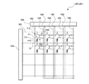
図2(a)、(b)に示すように、本実施形態の有機EL装置1は、ガラス等からなる透明な基板10と、基板10上にマトリックス状に配置された発光素子が具備された発光素子部11を具備している。なお、発光素子は陽極、機能層、陰極により構成されたものであり、機能層とは、正孔注入層、発光層、電子注入/輸送層等である。基板10は、例えばガラス等の透明基板であり、基板10の中央に位置する表示領域2aと、基板10の周縁に位置して表示領域2aの外側に非表示領域2bとに区画されている。表示領域2aは、マトリックス状に配置された発光素子によって形成される領域であり、有効表示領域とも言う。また、表示領域の外側に非表示領域2bが形成されている。そして、非表示領域2bには、表示領域2aに隣接するダミー表示領域2dが形成されている。また、図2(b)に示すように、発光素子部11と基板10の間には回路素子部14が備えられ、この回路素子部14に前述の走査線、信号線、保持容量、スイッチング用の薄膜トランジスタ、駆動用の薄膜トランジスタ123等が備えられている。また、陰極12は、その一端が基板10上に形成された陰極用配線12aに接続しており、この配線の一端部12bがフレキシブル基板5上の配線5aに接続されている。また、配線5aは、フレキシブル基板5上に備えられた駆動IC6(駆動回路)に接続されている。
As shown in FIGS. 2A and 2B, the
また、図2(a)及び図2(b)に示すように、回路素子部14の非表示領域2bには、前述の電源線103(103R、103G、103B)が配置されている。また、図2(a)に記載の表示領域2aの両側には、前述の走査側駆動回路105、105が配置されている。この走査側駆動回路105、105はダミー表示領域2dの下側の回路素子部14内に設けられている。更に回路素子部14内には、走査側駆動回路105、105に接続される駆動回路用制御信号配線105aと駆動回路用電源配線105bとが設けられている。更に図2(a)に記載の表示領域2aの上側(図面において上側、駆動IC6と反対側)には検査回路106が配置されている。この検査回路106により、製造途中や出荷時の有機EL装置の品質、欠陥の検査を行うことができる。
Further, as shown in FIGS. 2A and 2B, the power supply lines 103 (103R, 103G, and 103B) described above are arranged in the
また、図2(b)に示すように、発光素子部11は、複数の画素電極111…上の各々に積層された機能層110と、各画素電極111及び機能層110の間の平面領域に備えられて各機能層110を平面的に区画する無機物バンク層112aとを主体として構成されている。機能層110上には陰極12が配置されている。これら画素電極111、機能層110及び陰極12によって発光素子(例えば有機EL素子)が構成されている。ここで、画素電極111は、例えばITOにより形成されてなり、平面視略矩形にパターニングされて形成されている。この画素電極111の厚さは、例えば50〜200nmの範囲が好ましく、特に150nm程度がよい。隣接する画素電極111…の間に無機物バンク層112a(絶縁層)が備えられている。
Further, as shown in FIG. 2B, the light emitting
また図2(b)に示すように、発光素子部11上には封止部3が備えられている。この封止部3は、陰極12上に塗布された熱硬化樹脂あるいは紫外線硬化樹脂等からなる封止樹脂3aと、封止樹脂3a上に配置された封止基板3bとからなる。なお、封止樹脂3aとしては、硬化時にガス、溶媒等が発生しないものが好ましい。この封止部3は、少なくとも陰極12を覆うように形成されており、陰極12及び発光層110bに対する水又は酸素の侵入を防いで、陰極12及び発光層110bの酸化を防止する。なお、封止基板3bは、封止樹脂3aに接合されて封止樹脂3aを保護するものであり、ガラス板、金属板若しくは樹脂板のいずれかであることが好ましい。また後述するように、カン封止タイプのものも好ましく、凹んだ部分にゲッター材を配置し、ゲッター材により酸素の吸着を行い封止した内部の酸化を防止するようにしてもよい。
Further, as shown in FIG. 2B, the sealing
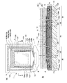
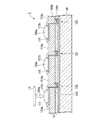
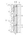
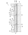
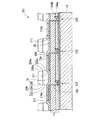
図3は、有機EL装置における発光素子について拡大した図であり、特に表示領域の断面構造を拡大した図を示す。この図3には3つの画素領域Aが図示されている。
この有機EL装置1は、基板10、その上に形成されたTFTなどの回路等を有する回路素子部14、並びに更にこの回路素子部14の上に形成された画素電極(陽極)111、正孔注入層110a及び発光層110bを含む機能層110、及び陰極12、を有する発光素子部11により構成されている。上記画素電極111、正孔注入層110a、発光層110b及び陰極12が有機EL素子を構成している。この有機EL装置1においては、機能層110から基板10側に発した光が、回路素子部14及び基板10を透過して基板10の下側(観測者側)に出射されると共に、機能層110から基板10の反対側に発した光が陰極12により反射されて、回路素子部14及び基板10を透過して基板10の下側(観測者側)に出射されるようになっている。
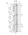
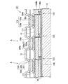
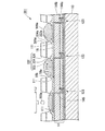
FIG. 3 is an enlarged view of the light emitting element in the organic EL device, and particularly shows an enlarged cross-sectional structure of the display region. In FIG. 3, three pixel regions A are shown.
The
無機物バンク層112aは、図3に示すように、発光領域を制御するものであり、画素電極111を区画するようにして画素電極111,111間に形成されている。また、無機物バンク層112aの一部が画素電極111の周縁部上に乗り上げて形成され、無機物バンク層112aと画素電極111とが平面視で一部重なっている。これにより、画素電極111上には、無機物バンク層112aによって区画された画素開口部112cが設けられ、この画素開口部112cの面積が開口率となる。
As shown in FIG. 3, the
ここで、無機物バンク層112aは、SiNに炭素(C)を微量に混合させた材料から形成されている。この無機物バンク層112a表面には酸素プラズマ処理とフッ化炭素系のガスを用いたプラズマ処理の連続処理、或いは上記混合ガスを用いたプラズマ処理が施され、無機物バンク層112a表面が撥液性となっている。
また、無機物バンク層112aを、例えばSiO2、SiN、TiO2等の無機材料を用いて形成することもできる。このとき、無機物バンク層112a表面には、トリメトキシシラン等のシラン系カップリング剤からなる単層膜が形成されており、無機物バンク層112a表面が撥液性となっている。これにより、無機物バンク層112aは、後述する正孔注入層形成材料に対して撥液性を有する一方、発光層形成材料に対しては正孔注入層形成材料と比較して親液性を有することになる。
Here, the
The
この無機物バンク層112aの膜厚は、狙いとする正孔注入層110aの膜厚と同程度にすることが好ましい。例えば、30〜200nmの範囲が好ましく、特に50nm〜100nmがよい。膜厚が薄すぎると絶縁性が確保できなくなり、厚すぎてもクラックがなく絶縁層を形成するのが困難になる。また膜厚が200nmを越えると、正孔注入層110a上に積層する後述の発光層110bの平坦性を確保できなくなるので好ましくない。
The film thickness of the
機能層110は、図3に示すように、画素電極111上に形成された正孔注入層110aと、正孔注入層110a上に積層された発光層110bとを有している。
As shown in FIG. 3, the
正孔注入層110aは、無機物バンク層112aによって区画された画素開口部112c内の画素電極111上に形成されている。本実施形態において無機物バンク層112a表面は撥液性となっている。そのため、正孔注入層110aを液相法により形成する際に、たとえ無機物バンク層112a上に正孔注入層形成材料が吐出されたとしてもはじかれて画素開口部112c内に流れ込み、画素開口部112cの外側には漏れ出さないようになっている。また、正孔注入層110aは、吐出量等の吐出条件を調整することにより、正孔注入層110aの上面の高さが、画素電極111上に乗り上げて形成される無機物バンク層112aの上面の高さと略同じとなるように形成されている。ここで、正孔注入層110a及び無機物バンク層112aの上面の高さは、例えば画素電極111の表面から50nmである。これにより、無機物バンク層112aの上面と正孔注入層110aの上面とで連続する平坦面が形成される。
The
なお、正孔注入層形成材料としては、例えば、ポリエチレンジオキシチオフェン(PEDOT)等のポリチオフェン誘導体とポリスチレンスルホン酸等の混合物が好適に用いられる。 As the hole injection layer forming material, for example, a mixture of a polythiophene derivative such as polyethylene dioxythiophene (PEDOT) and polystyrene sulfonic acid is preferably used.
発光層110bは、図3に示すように、無機物バンク層112a及び正孔注入層110a上の全面に形成されている。この発光層110bの高分子発光層形成材料としては、ポリフルオレン誘導体(PF)、ポリパラフェニレンビニレン誘導体(PPV)、ポリパラフェニレン誘導体(PPP)、ポリビニルカルバゾール(PVK)、ポリチオフェン誘導体、ポリメチルフェニルシラン(PMPS)等のポリシラン系などの高分子有機材料が好適に用いられる。発光層110bの膜厚としては例えば50〜80nmが好ましい。
As shown in FIG. 3, the
陰極12は、図3に示すように、発光層110b上の全面に画素電極111に対向して形成されている。この陰極12は、カルシウム(Ca)層とアルミニウム(Al)層とが基板10側からこの順に積層されて構成されている。Al層は、発光層110bから発光された光を基板10側(観察者側)に反射させるもので、Al層の他に、Ag層又はAl層とAg層との積層膜等から構成することも好ましい。また、発光層110bの材料を効率よく発光させるために、発光層110bと陰極12のCa層との間にフッ化リチウム(LiF)層を形成する場合もある。Ca層の膜厚としては、例えば2〜20nmの範囲が好ましく、特に10nm程度がよい。また、Al層の膜厚としては、例えば100〜1000nmの範囲が好ましく、特に200nm程度がよい。更にAl層上にSiO、SiO2、SiN等からなる酸化防止用の保護層を設けても良い。
As shown in FIG. 3, the
(有機EL装置の製造方法)
次に、第1の実施形態に係る有機EL装置の製造方法について、主に図4から図7を参照しつつ説明する。
なお、TFT等の製造工程については、公知の方法が用いられるので省略する。
(Method for manufacturing organic EL device)
Next, a method for manufacturing the organic EL device according to the first embodiment will be described with reference mainly to FIGS.
In addition, about the manufacturing process of TFT etc., since a well-known method is used, it abbreviate | omits.
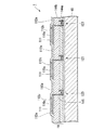
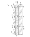
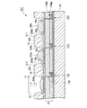
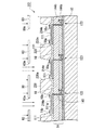
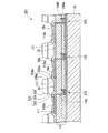
<バンク層形成工程>
まず、ケイ素(Si)、窒素(N)を含む材料に対して炭素(C)を含む材料を微量に混合させた材料を用いて、CVD法により画素電極111を含む第2層間絶縁膜144b上の全面に無機物バンク層となる絶縁層を成膜する。続けて、絶縁層上の全面に感光性レジストを塗布した後、画素電極111上の上記画素開口部112cに対応する位置が開口されたマスクを用いて、感光性レジストをフォトリソグラフィー処理し、感光性レジストを所定形状にパターニングする。そして、このパターニングした感光性レジストをマスクとして絶縁層をエッチング処理する。この処理により、図4に示すように、回路素子部14上に、画素電極111を区画すると共に、一部が画素電極111の周縁部上に乗り上げた無機物バンク層112aを形成する。また、無機物バンク層112aの膜厚は30〜200nmの範囲が好ましく、特に50nmが好ましい。そして、酸素ガスプラズマ処理、テトラフルオロメタンを処理ガスとするプラズマ処理(CF4プラズマ処理)により、無機物バンク層112a表面に撥液処理を施す。なお、フッ素系化合物ガスの雰囲気中に酸素ガスを混合させた処理ガスを用いてプラズマ処理を行っても良い。これにより、無機物バンク層112a表面の撥液性を調整することができる。
<Bank layer formation process>
First, on the second
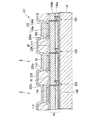
<正孔注入層形成工程>
次に、図5に示すように、PEDOT/PSS(PEDOT:PSS=1:6又は1:20)の混合物を含む水分散液にジエチレングリコール等の溶媒を添加した正孔注入層形成材料109aを、無機物バンク層112aに区画された画素開口部112c内にインクジェット装置IJにより吐出する。
ここで、無機物バンク層112a表面には撥液処理が施されており、無機物バンク層112a表面と正孔注入層形成材料109aとの接触角は約80°となっている。従って、無機物バンク層112aの画素開口部112cに吐出される正孔注入層形成材料109aが無機物バンク層112a上面に吐出されたとしても、正孔注入層形成材料109aははじかれ、画素開口部112c内に流れ込む。
<Hole injection layer forming step>
Next, as shown in FIG. 5, a hole injection
Here, the surface of the
また本実施形態では、インクジェット装置IJから吐出される正孔注入層形成材料109aの吐出量、及び吐出する正孔注入層形成材料109aの溶媒中に含有させるPEDOT/PSS等の固形分濃度を制御する。これにより、画素電極111の周縁部上に形成された無機物バンク層112aの上面の高さと、吐出した正孔注入層形成材料を乾燥した後の正孔注入層110aの上面との高さとを同じに形成することができる。
In this embodiment, the discharge amount of the hole injection
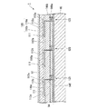
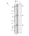
<乾燥工程>
次に、図6に示すように、吐出した正孔注入層形成材料に含まれる溶媒を乾燥処理により蒸発させて、無機物バンク層112aに区画された画素開口部112c内の画素電極111上に正孔注入層110aを形成する。詳細には、吐出した正孔注入層形成材料を、真空乾燥した後、大気圧中において200℃の温度で10分間乾燥させる。この乾燥処理によって、図6に示すように、画素電極111の周縁部上に形成される無機物バンク層112aの上面と同じ高さを有する正孔注入層110aを形成することができる。また、無機物バンク層112a表面には撥液処理が施されているため、無機物バンク層112a上には正孔注入層110aが形成されず、無機物バンク層112aの上面と正孔注入層110aの上面とで連続した平坦面が形成される。
<Drying process>
Next, as shown in FIG. 6, the solvent contained in the discharged hole injecting layer forming material is evaporated by a drying process, and positively applied to the
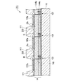
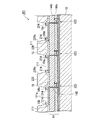
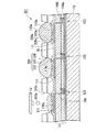
<発光層形成工程>
次に、無機物バンク層112a及び正孔注入層110a上の全面に、スピンコート法により発光層形成材料を成膜する。発光層形成材料としては、ポリフルオレン誘導体(PF)、ポリパラフェニレンビニレン誘導体(PPV)、ポリビニルカルバゾール、CBPとIr(ppy)3(イリジウム錯体)との混合物などが用いられ、これらの発光層形成材料をキシレンやトルエンに溶解させたものを塗布溶液として好適に用いることができる。
<Light emitting layer forming step>
Next, a light emitting layer forming material is formed on the entire surface of the
ここで、無機物バンク層112a表面は撥液性を有するが、発光層を形成する塗布溶液にはキシレン等の芳香族系材料が含有されているため、発光層形成材料の塗布液は正孔注入層形成材料109aに比べて、無機物バンク層112a表面に対する濡れ性がよくなっている。具体的には、正孔注入層110a表面と発光層形成材料の塗布液との接触角は約30°である。また、無機物バンク層112a表面と発光層形成材料の塗布液との接触角は約40°である。従って、正孔注入層110aの上面及び無機物バンク層112aの上面と、発光層形成材料の塗布液との接触角は略同じとなっている。
Here, although the surface of the
従って、スピンコート法により、図7に示すように、無機物バンク層112a及び正孔注入層110a上の全面に発光層110bが形成される。詳細には、スピンコート成膜後、不活性雰囲気中において130℃の温度で60分間アニール処理を施す。これにより、膜厚が例えば80nmの均一かつ平坦な発光層110bを形成することができる。
発光層を形成する塗布法としては、スピンコート法の他に、ディップコート法や、ノズルコート法、ブレードコート法などの方法を用いても良い。
Therefore, the
As a coating method for forming the light emitting layer, in addition to the spin coating method, a dip coating method, a nozzle coating method, a blade coating method, or the like may be used.
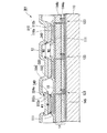
<陰極形成工程>
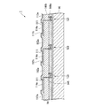
次に、図7に示すように、発光層110b上の全面に、真空加熱蒸着法により、Ca層及びAl層を順番に積層し、これらの積層膜から構成される陰極12を形成する。なお、上述したように、Ca層の下層にLiF層を形成しても良い。また陰極12上に、酸化防止のためにSiO2、SiN等の保護層を形成することも好ましい。
<Cathode formation process>
Next, as shown in FIG. 7, a Ca layer and an Al layer are sequentially laminated on the entire surface of the
最後に、図2(b)に戻り、熱硬化樹脂又は紫外線硬化樹脂からなる封止樹脂3aを陰極12上の全面に塗布し、封止樹脂3a上に封止基板3bを積層して封止部3を形成する。封止工程は、窒素、アルゴン、ヘリウム等の不活性ガス雰囲気で行うことが好ましい。
このような方法により第1実施形態に係る有機EL装置1を製造することができる。
Finally, returning to FIG. 2B, a sealing
With such a method, the
なお、上記実施形態では、正孔輸送層を省略したが、正孔注入層110aと発光層110bとの間に正孔輸送層を形成しても良い。正孔輸送層の材料としては、トリフェニルアミン系ポリマーを用いることができる。これにより、より効率よく正孔を発光層110bに注入することができるので、効率、寿命に優れた特性が得られる。
In the above embodiment, the hole transport layer is omitted, but a hole transport layer may be formed between the
本実施形態によれば、画素電極111の周縁部上に設けられる無機物バンク層112aは正孔注入層110aに対して撥液性を有するため、無機物バンク層112a上に吐出される正孔注入層110a形成材料ははじかれ、無機物バンク層112aに区画された画素開口部112c内に流れ込む。また、正孔注入層110aの上面の高さと無機物バンク層112aの上面の高さとは略同じであり、正孔注入層110a形成材料が無機物バンク層112a上に漏れ出さないように制御されている。そのため、正孔注入層110aは、無機物バンク層112aによって区画された画素開口部112c内の画素電極111上にのみ形成され、画素開口部112cの外側(隣接する画素間)の無機物バンク層112a上に配置されることはない。
従って、各画素電極111に設けられた正孔注入層110aの正孔が隣接する画素間に流れることに起因するいわゆるクロストークの発生を抑制することができる。よって、電流が隣接する画素間に滲みることによる発光形状輪郭ボケといった表示品質の低下を防止することができる。
According to this embodiment, since the
Therefore, it is possible to suppress the occurrence of so-called crosstalk caused by the holes in the
また本実施形態によれば、無機物バンク層112aの上面と正孔注入層110aの上面とは略同じ高さであるため、無機物バンク層112aの上面と正孔注入層110aの上面は連続した平坦面となる。従って、無機物バンク層112a及び正孔注入層110a上に形成される発光層110bは膜厚の均一かつ平坦な膜となり、輝度ムラのない、均一な発光を得ることができる。
Further, according to the present embodiment, since the top surface of the
また本実施形態によれば、無機物バンク層112a表面が撥液性を有するため、インクジェット装置を用いた場合でも、無機物バンク層112aに区画された画素開口部112cの外側に正孔注入層110a形成材料を漏れ出させることなく、選択的に正孔注入層110aを形成することができる。従って、インクジェット装置を用いることにより、材料の無駄を抑制することができ、低コストかつ高精度に正孔注入層110aを形成することができる。
Further, according to the present embodiment, since the surface of the
さらに本実施形態によれば、無機物バンク層112a及び正孔注入層110aの上面は連続した平坦面であるため、簡便なスピンコート法により発光層110bを形成することができる。これにより、膜厚の均一かつ平坦な発光層110bを容易に形成することができる。
Furthermore, according to this embodiment, since the top surfaces of the
[第2の実施形態]
次に、本発明の第2の実施形態について図8から図10を参照して説明する。
本実施形態と上記第1実施形態とでは、無機物バンク層112aに撥液処理を施す方法が異なる。なお、その他の有機EL装置の基本構成及び製造方法は、上記第1実施形態と同様であり、共通の構成要素には同一の符号を付し、詳細な説明は省略する。
[Second Embodiment]
Next, a second embodiment of the present invention will be described with reference to FIGS.
The present embodiment is different from the first embodiment in the method of applying a liquid repellent treatment to the
図8に示すように、画素電極111を含む無機物バンク層112a上の全面に、トリメトキシシラン等のシラン系カップリング剤114aを気相法或いはディッピング法により形成する。このとき、シラン系カップリング剤の末端の官能基を選択することにより、無機物バンク層112aの表層の濡れ性を制御することができる。
As shown in FIG. 8, a
次に、図9に示すように、上記画素開口部112cに対応する平面領域が開口されたマスクを、無機物バンク層112a上に設置する。そして、このマスク60を介して、画素電極111を含む無機物バンク層112a上に形成されたシラン系カップリング剤114aに紫外線を照射する。
Next, as shown in FIG. 9, a mask in which a planar region corresponding to the
この照射により、マスク60を通過した紫外線がシラン系カップリング剤114a上に到達し、図10に示すように、画素開口部112c、詳細には画素電極111上面及び無機物バンク層112aの側面に形成されるシラン系カップリング剤が除去される。そして、無機物バンク層112a上面にはシラン系カップリング剤からなる単層膜114が形成される。このようにして、無機物バンク層112a表面に撥液性を付与する。一方、画素開口部112c内の画素電極111上及び無機物バンク層112aの側面は、シラン系カップリング剤が除去されるため、単層膜114が形成されている無機物バンク層112a上面と比較して親液性の表面となる。
By this irradiation, the ultraviolet rays that have passed through the
<露光装置>
次に、上記実施形態において説明した有機EL装置1(露光ヘッド)を備える露光装置について説明する。なお、露光ヘッドには、有機EL素子が千鳥状に配列されたものが用いられている。
<Exposure device>
Next, an exposure apparatus including the organic EL device 1 (exposure head) described in the above embodiment will be described. As the exposure head, an organic EL element arranged in a staggered pattern is used.
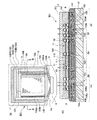
図11は、露光装置100の概略構成を示す斜視図である。
露光装置は、図11に示すように、露光ヘッド62と、この露光ヘッド62からの光を結像させるレンズアレイ31と、レンズアレイ31を透過した露光ヘッド62からの光によって露光される感光体ドラム9とを備えている。
この露光装置100によれば、上記有機EL装置を露光ヘッド62として備えているため、輝度ムラのない高品質の露光装置100を提供することができる。
FIG. 11 is a perspective view showing a schematic configuration of the
As shown in FIG. 11, the exposure apparatus includes an
According to the
[第3の実施の形態]
以下、本発明の実施形態について図面を参照しつつ説明する。
なお、図12〜図22において、各層や各部材を図面上で認識可能な程度の大きさとするため、各層や各部材に縮尺は実際のものとは異なるように表している。
また、本実施形態の有機EL装置は、発光層で発光した光を基板側から取り出すボトムエミッション方式である。
[Third Embodiment]
Embodiments of the present invention will be described below with reference to the drawings.
In FIGS. 12 to 22, the scales of the layers and the members are shown to be different from the actual scales so that the layers and the members can be recognized on the drawings.
In addition, the organic EL device of the present embodiment is a bottom emission method that extracts light emitted from the light emitting layer from the substrate side.
(有機EL装置)
図12(a)は本実施形態の有機EL装置の概略構成を示す平面図であり、図12(b)は(a)の有機EL装置のA−B線に沿った断面図である。
(Organic EL device)
FIG. 12A is a plan view showing a schematic configuration of the organic EL device of the present embodiment, and FIG. 12B is a cross-sectional view taken along the line AB of the organic EL device of FIG.
図1に示したように、本実施形態の有機EL装置201(発光装置)は、複数の走査線101と、走査線101に対して交差する方向に延びる複数の信号線102と、信号線102に並列に延びる複数の電源線103とがそれぞれ配線された回路構成を有する。走査線101及び信号線102の各交点付近に、画素領域Aが設けられている。
As shown in FIG. 1, the organic EL device 201 (light emitting device) of this embodiment includes a plurality of
信号線102には、シフトレジスタ、レベルシフタ、ビデオライン及びアナログスイッチ等を備えるデータ側駆動回路104が接続されている。また、走査線101には、シフトレジスタ及びレベルシフタ等を備える走査側駆動回路105が接続されている。さらに、画素領域Aの各々には、走査線101を介して走査信号がゲート電極に供給されるスイッチング用の薄膜トランジスタ112と、このスイッチング用の薄膜トランジスタ112を介して信号線102から共有される画素信号を保持する保持容量(cap)と、該保持容量(cap)によって保持された画素信号がゲート電極に供給される駆動用の薄膜トランジスタ123と、この駆動用の薄膜トランジスタ123を介して電源線103に電気的に接続したときに当該電源線103から駆動電流が与えられる画素電極111と、この画素電極111と陰極(対向電極)12との間に挟み込まれた機能層110とが設けられている。先の電極111と陰極12と機能層110により、発光素子例えば有機EL素子が構成されている。
To the
かかる構成によれば、走査線101が駆動されてスイッチング用の薄膜トランジスタ112がオンになると、そのときの信号線102の電位が保持容量capに保持され、該保持容量capに状態に応じて、駆動用の薄膜トランジスタ123のオン・オフ状態が決まる。そして、駆動用の薄膜トランジスタ123のチャネルを介して、電源線103から画素電極111に電流が流れ、さらに機能層110を介して陰極12に電流が流れる。機能層110は、これを流れる電流量に応じて発光する。
According to such a configuration, when the
図12(a)、(b)に示すように、本実施形態の有機EL装置201は、ガラス等からなる透明な基板10と、基板10上にマトリックス状に配置された発光素子が具備された発光素子部11を具備している。なお、発光素子は陽極、機能層、陰極により構成されたものであり、機能層とは、正孔注入層、発光層、電子注入/輸送層等である。基板10は、例えばガラス等の透明基板であり、基板10の中央に位置する表示領域2aと、基板10の周縁に位置して表示領域2aの外側に非表示領域2bとに区画されている。表示領域2aは、マトリックス状に配置された発光素子によって形成される領域であり、有効表示領域とも言う。また、表示領域の外側に非表示領域2bが形成されている。そして、非表示領域2bには、表示領域2aに隣接するダミー表示領域2dが形成されている。また、図12(b)に示すように、発光素子部11と基板10の間には回路素子部14が備えられ、この回路素子部14に前述の走査線、信号線、保持容量、スイッチング用の薄膜トランジスタ、駆動用の薄膜トランジスタ123等が備えられている。また、陰極12は、その一端が基板10上に形成された陰極用配線12aに接続しており、この配線の一端部12bがフレキシブル基板5上の配線5aに接続されている。また、配線5aは、フレキシブル基板5上に備えられた駆動IC6(駆動回路)に接続されている。
As shown in FIGS. 12A and 12B, the
また、図12(a)及び図12(b)に示すように、回路素子部14の非表示領域2bには、前述の電源線103(103R、103G、103B)が配置されている。また、図12(a)に記載の表示領域2aの両側には、前述の走査側駆動回路105、105が配置されている。この走査側駆動回路105、105はダミー表示領域2dの下側の回路素子部14内に設けられている。さらに回路素子部14内には、走査側駆動回路105、105に接続される駆動回路用制御信号配線105aと駆動回路用電源配線105bとが設けられている。さらに図12(a)に記載の表示領域2aの上側(図面において上側、駆動IC6と反対側)には検査回路106が配置されている。この検査回路106により、製造途中や出荷時の有機EL装置の品質、欠陥の検査を行うことができる。
Further, as shown in FIGS. 12A and 12B, the above-described power supply lines 103 (103R, 103G, and 103B) are arranged in the
また、図12(b)に示すように、発光素子部11は、複数の画素電極111…上の各々に積層された機能層110と、各画素電極111及び機能層110の間の平面領域に備えられて各機能層110を平面的に区画する無機物バンク層18(第1隔壁)とを主体として構成されている。機能層110上には陰極12が配置されている。これら画素電極111、機能層110及び陰極12によって発光素子(例えば有機EL素子)が構成されている。ここで、画素電極111は、例えばITOにより形成されてなり、平面視略矩形にパターニングされて形成されている。この画素電極111の厚さは、例えば50〜200nmの範囲が好ましく、特に150nm程度がよい。隣接する画素電極111…の間に無機物バンク層18(第1隔壁)が備えられている。
Further, as shown in FIG. 12B, the light emitting
また、図12(b)に示すように、発光素子部11上には封止部3が備えられている。この封止部3は、陰極12上に塗布された熱硬化樹脂あるいは紫外線硬化樹脂等からなる封止樹脂3aと、封止樹脂3a上に配置された封止基板3bとからなる。なお、封止樹脂3aとしては、硬化時にガス、溶媒等が発生しないものが好ましい。この封止部3は、少なくとも陰極12を覆うように形成されており、陰極12及び発光層110bに対する水又は酸素の侵入を防いで、陰極12及び発光層110bの酸化を防止する。なお、封止基板3bは、封止樹脂3aに接合されて封止樹脂3aを保護するものであり、ガラス板、金属板若しくは樹脂板のいずれかであることが好ましい。また後述するように、カン封止タイプのものも好ましく、凹んだ部分にゲッター材を配置し、ゲッター材により酸素の吸着を行い封止した内部の酸化を防止するようにしてもよい。
Further, as shown in FIG. 12B, the sealing
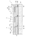
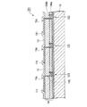
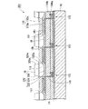
図13は、有機EL装置における発光素子について拡大した図であり、特に表示領域の断面構造を拡大した図を示す。この図13には3つの画素領域Aが図示されている。
有機EL装置201は、基板10、その上に形成されたTFTなどの回路等を有する回路素子部14、並びにさらにこの回路素子部14の上に形成された画素電極(陽極)111、正孔注入層110a及び発光層110bを含む機能層110、及び陰極12、を有する発光素子部11により構成されている。上記画素電極111、正孔注入層110a、発光層110b及び陰極12が有機EL素子を構成している。有機EL装置201においては、機能層110から基板10側に発した光が、回路素子部14及び基板10を透過して基板10の下側(観測者側)に出射されると共に、機能層110から基板10の反対側に発した光が陰極12により反射されて、回路素子部14及び基板10を透過して基板10の下側(観測者側)に出射されるようになっている。
FIG. 13 is an enlarged view of the light emitting element in the organic EL device, and particularly shows an enlarged cross-sectional structure of the display region. In FIG. 13, three pixel regions A are shown.
The
無機物バンク層18は、発光領域を制御するものであり、図13に示すように、画素電極111を区画するようにして画素電極111,111間に形成されている。また、無機物バンク層18の一部が画素電極111の周縁部上に乗り上げて形成され、無機物バンク層18と画素電極111とが平面視で一部重なっている。画素電極111上には、無機物バンク層18によって区画された画素開口部18cが設けられ、この画素開口部18cの面積が開口率となっている。なお、無機物バンク層18の膜厚は、例えば30〜200nmの範囲が好ましく、特に50〜100nmが好ましい。
The
ここで、無機物バンク層18は、SiNに炭素(C)を微量に混合させた材料からなる。この無機物バンク層18表面にはプラズマ処理が施され、無機物バンク層18表面が撥液性となっている。
また、無機物バンク層18を、例えばSiO2、TiO2、SiN等の無機材料を用いて構成することもできる。このとき、無機物バンク層18表面には、トリメトキシシラン等のシラン系カップリング剤からなる単層膜が形成されており、無機物バンク層18表面が撥液性となっている。
このように、無機物バンク層18は、後述する正孔注入層形成材料に対して撥液性を有する一方、発光層形成材料に対しては正孔注入層形成材料と比較して親液性を有する。
Here, the
Further, the
As described above, the
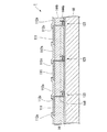
無機物バンク層18上には、図13に示すように、有機物バンク層220(第2隔壁)が形成されている。有機物バンク層220は、フォトリソグラフィー法の精度を考慮して、無機物バンク層18の周縁よりも内側に間隔を空けて形成されている。これにより、無機物バンク層の周縁部には有機物バンク層220の側面220aから突出した突出部18bが設けられる。有機物バンク層220の断面形状は、基板10面に対して鋭角に傾斜する傾斜面が設けられた台形状となっている。また、有機物バンク層220の側面220aは撥液処理されている。
On the
機能層110は、図13に示すように、画素電極111上に形成された正孔注入層110aと、正孔注入層110a上に積層された発光層110bとを有している。
As shown in FIG. 13, the
正孔注入層110aは、無機物バンク層18によって区画された画素開口部18c内の画素電極111上に形成されている。本実施形態において無機物バンク層18表面は撥液処理されている。そのため、正孔注入層110aを液相法により形成する際に、たとえ無機物バンク層18上に正孔注入層形成材料が吐出されたとしてもはじかれて無機物バンク層18内に流れ込み、画素開口部18cから漏れ出さないようになっている。また、正孔注入層110aの上面の高さは、吐出量等の吐出条件を調整することにより、画素電極111上に乗り上げた無機物バンク層18(突出部18b)の上面の高さと略同じとなるように形成されている。これにより、無機物バンク層18の上面と正孔注入層110aの上面とにより連続する平坦面が設けられる。
The
なお、正孔注入層形成材料としては、例えば、ポリエチレンジオキシチオフェン(PEDOT)等のポリチオフェン誘導体とポリスチレンスルホン酸等の混合物が好適に用いられる。 As the hole injection layer forming material, for example, a mixture of a polythiophene derivative such as polyethylene dioxythiophene (PEDOT) and polystyrene sulfonic acid is preferably used.
発光層110bは、図13に示すように、有機物バンク層220に区画された開口部220c内の正孔注入層110a上の全面に形成されている。発光層110bは、赤色(R)に発光する赤色発光層、緑色(G)に発光する緑色発光層、及び青色(B)に発光する青色発光層の3種類を有し、各発光層がストライプ状に配置されている。発光層110bの高分子発光層形成材料としては、ポリフルオレン(PF)誘導体、ポリパラフェニレンビニレン(PPV)誘導体、ポリパラフェニレン(PPP)誘導体、ポリビニルカルバゾール(PVK)、ポリチオフェン誘導体、ポリメチルフェニルシラン(PMPS)等のポリシラン系などの高分子有機材料が好適に用いられる。発光層110bの膜厚としては例えば50〜100nmが好ましい。
本実施形態において有機物バンク層220表面は撥液処理されている。そのため、開口部220c内に吐出された発光層形成材料は、隣接画素に漏れ出すことなく、所定の正孔注入層110a上、及び無機物バンク層18上の全面に成膜される。
As shown in FIG. 13, the
In the present embodiment, the surface of the
陰極12は、図13に示すように、発光層110bを含む有機物バンク層220上の全面に画素電極111に対向するようにして形成されている。この陰極12は、カルシウム(Ca)層とアルミニウム(Al)層とが基板10側からこの順に積層されて構成されている。Al層は、発光層110bから発光された光を基板10側(観察者側)に反射させるもので、Al層の他に、Ag層又はAl層とAg層との積層膜等から構成することも好ましい。また、発光層110bの材料を効率よく発光させるために、発光層110bと陰極12のCa層との間にフッ化リチウム(LiF)層を形成する場合もある。Ca層の膜厚としては、例えば2〜20nmの範囲が好ましく、特に10nm程度がよい。また、Al層の膜厚としては、例えば100〜1000nmの範囲が好ましく、特に200nm程度がよい。さらにAl層上にSiO、SiO2、SiN等からなる酸化防止用の保護層を設けても良い。
As shown in FIG. 13, the
(有機EL装置の製造方法)
次に、本実施形態に係る有機EL装置の製造方法について説明する。
図14〜図19は、第3の実施形態に係る有機EL装置の製造工程を示す断面図である。
なお、TFT等の製造工程については、公知の方法が用いられるので省略する。
(Method for manufacturing organic EL device)
Next, a method for manufacturing the organic EL device according to this embodiment will be described.
14 to 19 are cross-sectional views illustrating manufacturing steps of the organic EL device according to the third embodiment.
In addition, about the manufacturing process of TFT etc., since a well-known method is used, it abbreviate | omits.
<無機物バンク層形成工程>
まず、窒化ケイ素(SiN)に炭素(C)あるいは炭化ケイ素(SiC)を微量に混合させた材料を用いて、スパッタ法により画素電極111を含む第2層間絶縁膜144b上の全面に無機物バンク層となる絶縁層を成膜する。続けて、絶縁層上の全面に感光性レジストを塗布した後、画素電極111上の画素開口部18cに対応する位置が開口されたマスクを用いて、感光性レジストをフォトリソグラフィー処理し、感光性レジストを所定形状にパターニングする。そして、このパターニングした感光性レジストをマスクとして絶縁層をエッチング処理する。この処理により、図14に示すように、画素電極111を区画すると共に、一部が画素電極111の周縁部上に乗り上げた無機物バンク層18を形成する。また、無機物バンク層18の膜厚は30〜200nmの範囲が好ましく、特に50〜100nmが好ましい。
<Inorganic bank layer formation process>
First, an inorganic bank layer is formed on the entire surface of the second
<有機物バンク層形成工程>
次に、無機物バンク層18及び画素電極111上の全面に、スピンコート法によりアクリル、ポリイミド等の有機物バンク層形成材料を成膜する。
<Organic bank layer formation process>
Next, an organic bank layer forming material such as acrylic or polyimide is formed on the entire surface of the
次に、有機物バンク層形成材料上の全面に感光性レジストを塗布した後、無機物バンク層18に区画された画素開口部18cより広い開口になるよう開口部を有するマスクを用いて、感光性レジストをフォトリソグラフィー処理する。このとき、フォトリソグラフィー処理の精度を考慮して、無機物バンク層18の周縁よりも内側に有機物バンク層220の側面が形成されるように制御する。つまり、有機物バンク層220に区画される開口部の方が、無機物バンク層18に区画される画素開口部より開口面積が広くなるように、フォトリソグラフィー処理する。
Next, after applying a photosensitive resist on the entire surface of the organic bank layer forming material, the photosensitive resist is used by using a mask having an opening so as to have an opening wider than the
次に、パターニングした感光性レジストをマスクとして、有機物バンク層形成材料をエッチング処理する。このとき、有機物バンク層220が傾斜面を有する断面台形状となるようにエッチング液、エッチング時間等のエッチング条件を調節してエッチング処理する。このようにして、図15に示すように、無機物バンク層18上に有機物バンク層220を形成する。
Next, the organic bank layer forming material is etched using the patterned photosensitive resist as a mask. At this time, the etching is performed by adjusting the etching conditions such as the etching solution and the etching time so that the
<活性化処理工程>
次に、画素電極111の電極面、無機物バンク層18の表面18a、及び有機物バンク層220の表面に活性化処理を施す。活性化処理には、画素電極111における仕事関数の調整、制御、画素電極表面の洗浄、画素電極表面の親液化処理が含まれる。
まず、親液化処理として、大気雰囲気中で酸素を処理ガスとするプラズマ処理(O2プラズマ処理)を行う。このO2プラズマ処理により、画素電極111の電極面111a、及び無機物バンク層18の突出部18bの表面18a(以下、表面18aと省略する)が親液処理される。なお、このO2プラズマ処理は、親液性を付与するのみならず、上述の通り画素電極であるITO上の洗浄,仕事関数の調整も兼ねている。
<Activation process>
Next, an activation process is performed on the electrode surface of the
First, as a lyophilic process, a plasma process (O 2 plasma process) using oxygen as a process gas is performed in an air atmosphere. By this O 2 plasma treatment, the
次に、撥液化処理として、大気雰囲気中でテトラフルオロメタンを処理ガスとするプラズマ処理(CF4プラズマ処理)を行う。なお、処理ガスは、テトラフルオロメタン(四フッ化炭素)に限らず、他のフルオロカーボン系のガスを用いることができる。CF4プラズマ処理により、無機物バンク層18の表面18a並びに、有機物バンク層220の表層が撥液処理される。無機物バンクの方が有機物バンクに比べ、炭素含有量が少ないので、有機物バンクよりは低い撥液性を示す。また、O2プラズマにより前処理した方がフッ素化されやすいという特徴を有しており、本実施形態には特に有効である。なお、画素電極111の電極面111aもこのCF4プラズマ処理の影響を多少受けるが、濡れ性に影響を与えることは少ない。
Next, plasma treatment (CF 4 plasma treatment) using tetrafluoromethane as a treatment gas is performed as an lyophobic treatment in an air atmosphere. The processing gas is not limited to tetrafluoromethane (carbon tetrafluoride), and other fluorocarbon gases can be used. By the CF 4 plasma treatment, the
<正孔注入層形成工程>
次に、図16に示すように、PEDOT/PSS(PEDOT:PSS=1:6又は1:20)の混合物を含む水分散液にジエチレングリコール等の溶媒を添加した正孔注入層形成材料109aを、無機物バンク層18に区画された無機物バンク層18内にインクジェット装置IJにより吐出する。
ここで、無機物バンク層18表面には撥液処理が施されており、無機物バンク層18の表面18aと正孔注入層形成材料109aとの接触角は約80°となっている。従って、無機物バンク層18の無機物バンク層18に吐出される正孔注入層形成材料109aが無機物バンク層18の突出部18b上に吐出されたとしても、正孔注入層形成材料109aははじかれ、画素開口部18c内に流れ込む。
<Hole injection layer forming step>
Next, as shown in FIG. 16, a hole injection
Here, the surface of the
また本実施形態では、インクジェット装置IJから吐出される正孔注入層形成材料109aの吐出量、及び吐出する正孔注入層形成材料109aの溶媒中に含有させるPEDOT/PSS等の固形分濃度を制御する。これにより、画素電極111の周縁部上に形成される無機物バンク層18の上面の高さと、吐出した正孔注入層形成材料109aを乾燥した後の正孔注入層110aの上面との高さとを同じに形成することができる。
In this embodiment, the discharge amount of the hole injection
<乾燥工程>
次に、図17に示すように、吐出した正孔注入層形成材料に含有する溶媒を乾燥処理により蒸発させて、無機物バンク層18に区画された無機物バンク層18内の画素電極111上に正孔注入層110aを形成する。詳細には、吐出した正孔注入層形成材料を、真空乾燥した後、大気圧中において200℃の温度で10分間乾燥させる。この乾燥処理によって、図17に示すように、画素電極111の周縁部上に形成される無機物バンク層18の上面と同じ高さを有する正孔注入層110aを形成することができる。また、無機物バンク層18の表面18aには撥液処理が施されているため、無機物バンク層18上には正孔注入層110aが残っておらず、無機物バンク層18の上面と正孔注入層110aの上面とで連続した平坦面となる。
<Drying process>
Next, as shown in FIG. 17, the solvent contained in the discharged hole injection layer forming material is evaporated by a drying process, and is positively applied onto the
<発光層形成工程>
次に、図18に示すように、有機物バンク層220に区画された開口部220c内の無機物バンク層18の突出部18b及び正孔注入層110a上の全面に、インクジェット装置IJにより発光層形成材料113aを吐出する。発光層形成材料113aとしては、ポリフルオレン(PF)誘導体、ポリパラフェニレンビニレン(PPV)誘導体を芳香族系炭化水素溶媒で溶解した溶液が用いられる。芳香族系炭化水素溶媒としては、トリメチルベンゼン、シクロへキシルベンゼン、ドデシルベンゼン等のアルキル基のついたベンゼン溶媒、エーテル基のついたメトキシエトシキベンゼン等を用いても良い。
<Light emitting layer forming step>
Next, as shown in FIG. 18, the light emitting layer forming material is formed on the entire surface of the
ここで、有機物バンク層220の表層は撥液性を有しているため、吐出された発光層形成材料113aは、バンク層表面ではじかれて、隣接画素(開口部)に漏れ出したり、混入することなく開口部220c内に収まる。また、無機物バンク層18の表面18aも撥液性を有するが、有機物バンク層の表面の撥液性に比べると低く、発光層形成材料113aには表面張力の低い芳香族系材料が含有されているため、発光層形成材料の、正孔注入層表面と無機物バンク層18の表面18aに対する濡れ性(接触角)には大きな差が無いため、発光層形成材料113aは、正孔注入層110a表面並びに、無機物バンク層18の表面18a上にも均一に濡れ広がらせることができる。
具体的には、正孔注入層110a表面と発光層形成材料113aとの接触角は約40°である。また、無機物バンク層112a表面と発光層形成材料113aとの接触角は約50°である。従って、正孔注入層110aの上面及び無機物バンク層112aの上面と、発光層形成材料との接触角は略同じとなっている。
Here, since the surface layer of the
Specifically, the contact angle between the surface of the
次に、図19に示すように、インクジェット吐出により塗り分けされた発光層形成材料113aに含有する溶媒を乾燥処理により蒸発させて、無機物バンク層18及び正孔注入層110a上の全面に発光層110bを形成する。詳細には、吐出した発光層形成材料113aを、真空による溶媒除去後、さらにArや窒素などの不活性雰囲気中において130℃の温度で60分間アニール処理を施す。従って、発光層の膜厚が例えば80nmの均一な発光層110bを形成することができる。
Next, as shown in FIG. 19, the solvent contained in the light emitting
<陰極形成工程>
次に、図20に示すように、発光層110b上の全面に、真空加熱蒸着法により、Ca層及びAl層を順番に積層し、これらの積層膜から構成される陰極12を形成する。なお、上述したように、Ca層の下層にLiF層を形成しても良い。また陰極12上に、酸化防止のためにSiO2、SiN等の保護層を形成することも好ましい。
<Cathode formation process>
Next, as shown in FIG. 20, a Ca layer and an Al layer are sequentially laminated on the entire surface of the
最後に、図12(b)に戻り、熱硬化樹脂又は紫外線硬化樹脂からなる封止樹脂3aを陰極12上の全面に塗布し、封止樹脂3a上に封止基板3bを積層して封止部3を形成する。封止工程は、窒素、アルゴン、ヘリウム等の不活性ガス雰囲気で行うことが好ましい。
このような方法により有機EL装置201を製造することができる。
Finally, returning to FIG. 12B, a sealing
The
なお、上記実施形態では、正孔輸送層を省略したが、正孔注入層110aと発光層110bとの間に正孔輸送層を形成しても良い。正孔輸送層の材料としては、トリフェニルアミン系ポリマーを用いることができる。これにより、より正孔を発光層110bに注入することができるので、効率、寿命に優れた特性が得られる。
In the above embodiment, the hole transport layer is omitted, but a hole transport layer may be formed between the
本実施形態によれば、無機物バンク層18は正孔注入層110aに対して撥液性を有するため、無機物バンク層18上に吐出される正孔注入層形成材料109aははじかれ、無機物バンク層18に区画された画素開口部18c内に流れ込む。また、正孔注入層110aの上面の高さと無機物バンク層18の上面の高さとは略同じであり、正孔注入層形成材料が無機物バンク層18上に漏れ出さないように制御されている。そのため、正孔注入層110aが、無機物バンク層18によって区画された画素開口部18cから外側に配置されることはない。このように、無機物バンク層18の上面と正孔注入層110aの上面とは略同じ高さであるため、均一かつ平坦な正孔注入層110a及び発光層110bを形成することができる。さらに、正孔注入層110a及び発光層110bの周縁部と中央部とで膜厚を均一にすることができるため、発光寿命ムラのなく、発光寿命の均一化を図ることができる。
According to the present embodiment, since the
[第4の実施形態]
次に、本発明の第4の実施形態について図面を参照して説明する。
本実施形態と上記第3実施形態とでは、無機物バンク層に撥液処理を施す方法が異なる。なお、その他の有機EL装置の基本構成及び製造方法は、上記第3実施形態と同様であり、共通の構成要素には同一の符号を付し、詳細な説明は省略する。
[Fourth Embodiment]
Next, a fourth embodiment of the present invention will be described with reference to the drawings.
This embodiment is different from the third embodiment in the method of applying a liquid repellent treatment to the inorganic bank layer. The basic configuration and manufacturing method of the other organic EL devices are the same as those in the third embodiment, and common constituent elements are denoted by the same reference numerals and detailed description thereof is omitted.
図21及び図22は、本実施形態に係る有機EL装置の製造工程を示す断面図である。
まず、画素電極111を含む第2層間絶縁膜144b上の全面に、CVD法、スパッタ法、蒸着法等により、SiO2、TiO2等の無機物材料を成膜する。続けて、フォトリソグラフィー処理、エッチング処理により、図21に示すように、無機物バンク層18を形成する。
21 and 22 are cross-sectional views showing the manufacturing process of the organic EL device according to this embodiment.
First, an inorganic material such as SiO 2 or TiO 2 is formed on the entire surface of the second
次に、図21に示すように、無機物バンク層18上に、ポリイミド又はアルカリからなる有機物バンク層220を形成する。
Next, as shown in FIG. 21, an
次に、画素電極111、無機物バンク層18、及び有機物バンク層220のそれぞれの表面に、O2及びCF4の処理ガスを用いて連続プラズマ処理する。このプラズマ処理により、画素電極111の電極面111a及び無機物バンク層18の表面18aが親液処理される。一方、有機物バンク層220の側面220aが撥液処理される。
Next, continuous plasma treatment is performed on the surfaces of the
次に、トリメトキシシラン等のシラン系カップリング剤溶液に、プラズマ処理を施した上記基板を浸漬する。これにより、図21に示すように、親液処理された無機物バンク層18の表面18a及び、画素電極の電極面111a上にカップリング剤の単層膜214aが形成される。
Next, the substrate subjected to the plasma treatment is immersed in a silane coupling agent solution such as trimethoxysilane. Thereby, as shown in FIG. 21, a
続けて、図21に示すように、画素開口部18cの対応する位置に開口部60aを有するマスク60を用い、このマスクを介して紫外線を照射することにより、電極面111a上及び無機物バンク層18の側面のシラン系カップリング剤を除去する。
このようにして、図22に示すように、無機物バンク層18の表面18a(突出部18bの上面)にのみシラン系カップリング剤214を形成する。シラン系カップリング剤は、酸化物との密着性も良く、末端の官能基を選択することにより、正孔注入層形成材料等のインクとの濡れ性を調整することができる。
Subsequently, as shown in FIG. 21, by using a
In this way, as shown in FIG. 22, the
本実施形態によっても、上記第3実施形態と同様の作用効果を奏することができる。 Also according to the present embodiment, the same effects as those of the third embodiment can be achieved.
[第5の実施の形態]
以下、本発明の第5の実施形態について図面を参照して説明する。
また、本実施形態の有機EL装置は、発光層で発光した光を基板側から取り出すボトムエミッション方式である。
[Fifth Embodiment]
The fifth embodiment of the present invention will be described below with reference to the drawings.
In addition, the organic EL device of the present embodiment is a bottom emission method that extracts light emitted from the light emitting layer from the substrate side.
(有機EL装置)
図23(a)は有機EL装置の概略構成を示す平面図であり、図23(b)は(a)の有機EL装置のA−B線に沿った断面図である。
(Organic EL device)
FIG. 23A is a plan view showing a schematic configuration of the organic EL device, and FIG. 23B is a cross-sectional view of the organic EL device of FIG.
図1に示したように、本実施形態の有機EL装置301(発光装置)は、複数の走査線101と、走査線101に対して交差する方向に延びる複数の信号線102と、信号線102に並列に延びる複数の電源線103とがそれぞれ配線された回路構成を有する。走査線101及び信号線102の各交点付近に、画素領域Aが設けられている。
As shown in FIG. 1, the organic EL device 301 (light emitting device) of the present embodiment includes a plurality of
信号線102には、シフトレジスタ、レベルシフタ、ビデオライン及びアナログスイッチ等を備えるデータ側駆動回路104が接続されている。また、走査線101には、シフトレジスタ及びレベルシフタ等を備える走査側駆動回路105が接続されている。さらに、画素領域Aの各々には、走査線101を介して走査信号がゲート電極に供給されるスイッチング用の薄膜トランジスタ112と、このスイッチング用の薄膜トランジスタ112を介して信号線102から共有される画素信号を保持する保持容量(cap)と、該保持容量(cap)によって保持された画素信号がゲート電極に供給される駆動用の薄膜トランジスタ123と、この駆動用の薄膜トランジスタ123を介して電源線103に電気的に接続したときに当該電源線103から駆動電流が与えられる画素電極111と、この画素電極111と陰極(対向電極)12との間に挟み込まれた機能層110とが設けられている。先の電極111と陰極12と機能層110により、発光素子例えば有機EL素子が構成されている。
To the
かかる構成によれば、走査線101が駆動されてスイッチング用の薄膜トランジスタ112がオンになると、そのときの信号線102の電位が保持容量capに保持され、該保持容量capに状態に応じて、駆動用の薄膜トランジスタ123のオン・オフ状態が決まる。そして、駆動用の薄膜トランジスタ123のチャネルを介して、電源線103から画素電極111に電流が流れ、さらに機能層110を介して陰極12に電流が流れる。機能層110は、これを流れる電流量に応じて発光する。
According to such a configuration, when the
図23(a)、(b)に示すように、本実施形態の有機EL装置301は、ガラス等からなる透明な基板10と、基板10上にマトリックス状に配置された発光素子が具備された発光素子部11を具備している。なお、発光素子は陽極、機能層、陰極により構成されたものであり、機能層とは、正孔注入層、発光層、電子注入/輸送層等である。基板10は、例えばガラス等の透明基板であり、基板10の中央に位置する表示領域2aと、基板10の周縁に位置して表示領域2aの外側に非表示領域2bとに区画されている。表示領域2aは、マトリックス状に配置された発光素子によって形成される領域であり、有効表示領域とも言う。また、表示領域の外側に非表示領域2bが形成されている。そして、非表示領域2bには、表示領域2aに隣接するダミー表示領域2dが形成されている。また、図23(b)に示すように、発光素子部11と基板10の間には回路素子部14が備えられ、この回路素子部14に前述の走査線、信号線、保持容量、スイッチング用の薄膜トランジスタ、駆動用の薄膜トランジスタ123等が備えられている。また、陰極12は、その一端が基板10上に形成された陰極用配線12aに接続しており、この配線の一端部12bがフレキシブル基板5上の配線5aに接続されている。また、配線5aは、フレキシブル基板5上に備えられた駆動IC6(駆動回路)に接続されている。
As shown in FIGS. 23A and 23B, the
また、図23(a)及び図23(b)に示すように、回路素子部14の非表示領域2bには、前述の電源線103(103R、103G、103B)が配置されている。また、図23(a)に記載の表示領域2aの両側には、前述の走査側駆動回路105、105が配置されている。この走査側駆動回路105、105はダミー表示領域2dの下側の回路素子部14内に設けられている。さらに回路素子部14内には、走査側駆動回路105、105に接続される駆動回路用制御信号配線105aと駆動回路用電源配線105bとが設けられている。さらに図23(a)に記載の表示領域2aの上側(図面において上側、駆動IC6と反対側)には検査回路106が配置されている。この検査回路106により、製造途中や出荷時の有機EL装置の品質、欠陥の検査を行うことができる。
Further, as shown in FIGS. 23A and 23B, the above-described power supply lines 103 (103R, 103G, and 103B) are arranged in the
また、図23(b)に示すように、発光素子部11は、複数の画素電極111…上の各々に積層された機能層110と、各画素電極111及び機能層110の間の平面領域に備えられて各機能層110を平面的に区画する無機物バンク層18とを主体として構成されている。機能層110上には陰極12が配置されている。これら画素電極111、機能層110及び陰極12によって発光素子(例えば有機EL素子)が構成されている。ここで、画素電極111は、例えばITOにより形成されてなり、平面視略矩形にパターニングされて形成されている。この画素電極111の厚さは、例えば50〜200nmの範囲が好ましく、特に150nm程度がよい。隣接する画素電極111…の間に無機物バンク層18(第1隔壁)が備えられている。
Further, as shown in FIG. 23 (b), the light emitting
また、図23(b)に示すように、発光素子部11上には封止部3が備えられている。この封止部3は、陰極12上に塗布された熱硬化樹脂あるいは紫外線硬化樹脂等からなる封止樹脂3aと、封止樹脂3a上に配置された封止基板3bとからなる。なお、封止樹脂3aとしては、硬化時にガス、溶媒等が発生しないものが好ましい。この封止部3は、少なくとも陰極12を覆うように形成されており、陰極12及び発光層110bに対する水又は酸素の侵入を防いで、陰極12及び発光層110bの酸化を防止する。なお、封止基板3bは、封止樹脂3aに接合されて封止樹脂3aを保護するものであり、ガラス板、金属板若しくは樹脂板のいずれかであることが好ましい。また後述するように、カン封止タイプのものも好ましく、凹んだ部分にゲッター材を配置し、ゲッター材により酸素の吸着を行い封止した内部の酸化を防止するようにしてもよい。
Further, as shown in FIG. 23B, the sealing
図24は、有機EL装置における発光素子について拡大した図であり、特に表示領域の断面構造を拡大した図を示す。この図24には3つの画素領域Aが図示されている。
この有機EL装置301は、基板10、その上に形成されたTFTなどの回路等を有する回路素子部14、並びにさらにこの回路素子部14の上に形成された画素電極(陽極)111、正孔注入層110a及び発光層110bを含む機能層110、及び陰極12、を有する発光素子部11により構成されている。上記画素電極111、正孔注入層110a、発光層110b及び陰極12が有機EL素子を構成することができる。この有機EL装置301においては、機能層110から基板10側に発した光が、回路素子部14及び基板10を透過して基板10の下側(観測者側)に出射されると共に、機能層110から基板10の反対側に発した光が陰極12により反射されて、回路素子部14及び基板10を透過して基板10の下側(観測者側)に出射されるようになっている。
FIG. 24 is an enlarged view of the light emitting element in the organic EL device, and particularly shows an enlarged cross-sectional structure of the display region. FIG. 24 shows three pixel regions A.
The
無機物バンク層18は、発光領域を制御するものであり、図24に示すように、画素電極111を区画するようにして画素電極111,111間に形成されている。また、無機物バンク層18の一部が画素電極111の周縁部上に乗り上げて形成され、無機物バンク層18と画素電極111とが平面視で一部重なっている。これにより、画素電極111上には、無機物バンク層18によって区画された画素開口部18cが設けられ、この画素開口部18cの面積が開口率となる。また、無機物バンク層18は、例えば、SiO2、TiO2、SiN等の無機材料あるいはSiNに微量の炭素が含まれた材料からなる。この無機物バンク層18の膜厚は、例えば30〜200nmの範囲が好ましく、特に50〜100nmが好ましい。
The
無機物バンク層18上には有機物バンク層320が形成されている。有機物バンク層320は、フォトリソグラフィー処理の精度を考慮して、無機物バンク層18の周縁よりも内側に間隔を空けて形成されている。これにより、無機物バンク層の周縁部には、有機物バンク層320の側面から画素電極111中央部側へ突出した突出部18bが設けられる。
An
本実施形態において有機物バンク層320は、基板10側から第1有機物層322、酸化物層(隔壁部絶縁層)324、及び第2有機物層326が順に積層されて構成される。有機物バンク層320の形状は、傾斜面を有する断面台形状に形成されている。第1有機物層322及び第2有機物層326はアクリル又はポリイミドからなり、酸化物層324はSiO2、TiO2からなる。また、第1有機物層322の側面322a及び第2有機物層326の側面326aには撥液処理が施されており、酸化物層324の側面324aには親液処理が施されている。つまり、酸化物層324の側面324aは、第1有機物層322の側面322a等よりも相対的に撥液性が低い領域となっており、この酸化物層324の側面324aがピニングポイントとなる。
ここで、第1有機物層322の膜厚は、狙いとする発光層の膜厚と同程度であることが好ましい。具体的には、50〜100nmが好ましい。第2有機物層326の膜厚としては、0.5μm〜2μmが好ましい。酸化物層324の膜厚としては20nm〜50nmと薄い方が好ましい。酸化物層324の膜厚が厚くなると、酸化物層324の表面のピニングポイントの範囲も広くなり、ピニングポイントを一定の位置に制御(固定)することができないからである。なお、有機物バンク層320の酸化物層324に代えて、SiN等の材料を用いた層を形成することも可能である。
In this embodiment, the
Here, the film thickness of the first
機能層110は、図24に示すように、画素電極111上に形成された正孔注入層110aと、正孔注入層110a上に積層された発光層110bとを有している。
As shown in FIG. 24, the
正孔注入層110aは、図24に示すように、無機物バンク層18によって区画された画素開口部18c内の画素電極111上に形成されている。また、正孔注入層110aの周縁部は、無機物バンク層18の突出部18bに乗り上げて形成されている。正孔注入層形成材料としては、例えば、ポリエチレンジオキシチオフェン(PEDOT)等のポリチオフェン誘導体とポリスチレンスルホン酸(PSS)等の混合物(PEDOT/PSS)が好適に用いられる。
As shown in FIG. 24, the
発光層110bは、図24に示すように、有機物バンク層320に区画された開口部320c内の正孔注入層110a上の全面に形成されている。
ここで、発光層の外縁は、有機物バンク層320の酸化物層324のピニングポイントとなる側面324aと接触しており、発光層110bの上面の高さが、有機物バンク層320の酸化物層324の高さまで形成されている。発光層110bは、赤色(R)に発光する赤色発光層、緑色(G)に発光する緑色発光層、及び青色(B)に発光する青色発光層の3種類を有し、各発光層がストライプ状に配置されている。発光層110bの高分子発光層形成材料としては、ポリフルオレン(PF)誘導体、ポリパラフェニレンビニレン(PPV)誘導体、ポリパラフェニレン(PPP)誘導体(PPP)、ポリビニルカルバゾール(PVK)、ポリチオフェン誘導体、ポリメチルフェニルシラン(PMPS)等のポリシラン系などの高分子有機材料が好適に用いられる。発光層110bの膜厚としては例えば50〜100nmが好ましい。
The
Here, the outer edge of the light emitting layer is in contact with a
陰極12は、図24に示すように、発光層110bを含む有機物バンク層320上の全面に画素電極111に対向するようにして形成されている。この陰極12は、カルシウム(Ca)層とアルミニウム(Al)層とが基板10側からこの順に積層されて構成されている。Al層は、発光層110bから発光された光を基板10側(観察者側)に反射させるもので、Al層の他に、Ag層又はAl層とAg層との積層膜等から構成することも好ましい。また、発光層110bの材料を効率よく発光させるために、発光層110bと陰極12のCa層との間にフッ化リチウム(LiF)層を形成する場合もある。Ca層の膜厚としては、例えば2〜20nmの範囲が好ましく、特に10nm程度がよい。また、Al層の膜厚としては、例えば100〜1000nmの範囲が好ましく、特に200nm程度がよい。さらにAl層上にSiO、SiO2、SiN等からなる酸化防止用の保護層を設けても良い。
As shown in FIG. 24, the
(有機EL装置の製造方法)
次に、第5の実施形態に係る有機EL装置の製造方法について説明する。
図25〜図34は、第5の実施形態に係る有機EL装置の製造工程を示す断面図である。
なお、TFT等の製造工程については、公知の方法が用いられるので省略する。
(Method for manufacturing organic EL device)
Next, a method for manufacturing an organic EL device according to the fifth embodiment will be described.
FIG. 25 to FIG. 34 are cross-sectional views illustrating manufacturing steps of the organic EL device according to the fifth embodiment.
In addition, about the manufacturing process of TFT etc., since a well-known method is used, it abbreviate | omits.
<無機物バンク層形成工程>
まず、CVD法、コート法、スパッタ法、蒸着法等により、SiO2又はTiO2等の無機物バンク層となる絶縁層を、画素電極111を含む第2層間絶縁膜144b上の全面に成膜する。
続けて、絶縁層上の全面に感光性レジストを塗布した後、画素開口部18cに対応する位置が開口されたマスクを用いて、感光性レジストをフォトリソグラフィー処理し、感光性レジストを所定形状にパターニングする。そして、このパターニングした感光性レジストをマスクとして絶縁層をエッチング処理する。この処理により、図25に示すように、画素電極111を区画すると共に、一部が画素電極111の周縁部上に乗り上げた無機物バンク層18を形成する。
<Inorganic bank layer formation process>
First, an insulating layer to be an inorganic bank layer such as SiO 2 or TiO 2 is formed on the entire surface of the second
Subsequently, after applying a photosensitive resist on the entire surface of the insulating layer, the photosensitive resist is subjected to photolithography using a mask having an opening corresponding to the
<有機物バンク層形成工程>
次に、図26に示すように、無機物バンク層18及び画素電極111上の全面に、スピンコート法によりアクリル、ポリイミド等の第1有機物層形成材料322bを成膜する。
続けて、図26に示すように、成膜した第1有機物層形成材料322b上の全面に、CVD法、スパッタ法、蒸着法等によりSiO2、TiO2等の酸化物層形成材料324bを成膜する。
続けて、図26に示すように、成膜した無機物材料上の全面に、スピンコート法によりアクリル、ポリイミド等の第2有機物層形成材料326bを成膜する。
<Organic bank layer formation process>
Next, as shown in FIG. 26, a first organic
Subsequently, as shown in FIG. 26, an oxide
Subsequently, as shown in FIG. 26, a second organic
次に、第2有機物層形成材料326b上の全面に感光性レジストを塗布した後、無機物バンク層18に区画された画素開口部18cに対応する位置が、若干開口されたマスクを用いて、感光性レジストをフォトリソグラフィー処理する。このとき、フォトリソグラフィー処理の精度を考慮して、無機物バンク層18の周縁よりも内側に有機物バンク層320の側面が形成されるように制御する。つまり、有機物バンク層320に区画される開口部よりも、無機物バンク層18に区画される画素開口部の開口面積が広くなるように、フォトリソグラフィー処理する。
Next, after applying a photosensitive resist on the entire surface of the second organic
次に、パターニングした感光性レジストをマスクとして、第1有機物層形成材料322b、酸化物層形成材料324b、及び第2有機物層形成材料326bを一括エッチング処理する。このとき、有機物バンク層320が傾斜面を有する断面台形状となるように、エッチング液、エッチング時間等のエッチング条件を調節してエッチング処理する。このようにして、図27に示すように、無機物バンク層18上に第1有機物層322、酸化物層324、第2有機物層326の3層からなる有機物バンク層320を形成する。なお、無機物バンク層18の第1有機物層322の膜厚を調整することにより、酸化物層324の高さを調整することができる。これにより、ピニングポイントの位置を制御することができる。
Next, the first organic
<活性化処理工程>
次に、画素電極111の電極面、無機物バンク層18の表面、及び有機物バンク層表面に活性化処理を施す。活性化処理には、画素電極111における仕事関数の調整、制御、画素電極表面の洗浄、画素電極表面、無機物層及び酸化物層表面の親液化処理が含まれる。
まず、親液化処理として、大気雰囲気中で酸素を処理ガスとするプラズマ処理(O2プラズマ処理)を行う。このO2プラズマ処理により、画素電極111の電極面111a、無機物バンク層18の突出部18bの表面18a(以下、表面18aと省略する)、及び有機物バンク層320の酸化物層324の側面324aが親液処理される。なお、このO2プラズマ処理は、親液性を付与するのみならず、上述の通り画素電極であるITO上の洗浄,仕事関数の調整も兼ねている。
<Activation process>
Next, an activation process is performed on the electrode surface of the
First, as a lyophilic process, a plasma process (O 2 plasma process) using oxygen as a process gas is performed in an air atmosphere. By this O 2 plasma treatment, the
次に、撥液化処理として、大気雰囲気中でテトラフルオロメタンを処理ガスとするプラズマ処理(CF4プラズマ処理)を行う。なお、処理ガスは、テトラフルオロメタン(四フッ化炭素)に限らず、他のフルオロカーボン系のガスを用いることができる。CF4プラズマ処理により、有機物バンク層320の第1有機物層322の側面322a、第2有機物層326の側面326a及びその上面326cが撥液処理される。また、O2プラズマにより前処理した方がフッ素化されやすいという特徴を有しており、本実施形態には特に有効である。なお、画素電極111の電極面111a、無機物バンク層18の表面18a、及び第2有機物層326の酸化物層324の側面324aもこのCF4プラズマ処理の影響を多少受けるが、濡れ性に影響を与えることは少ない。
Next, plasma treatment (CF 4 plasma treatment) using tetrafluoromethane as a treatment gas is performed as an lyophobic treatment in an air atmosphere. The processing gas is not limited to tetrafluoromethane (carbon tetrafluoride), and other fluorocarbon gases can be used. By the CF 4 plasma treatment, the
<正孔注入層形成工程>
次に、図28に示すように、PEDOT/PSS(PEDOT:PSS=1:6又は1:20)の混合物を含む水分散液にジエチレングリコール等の溶媒を添加した正孔注入層形成材料109aを、無機物バンク層18に区画された画素開口部18c内にインクジェット装置IJにより吐出する。吐出された正孔注入層形成材料109aは、画素電極111の電極面111a上及び無機物バンク層18の突出部18b上に配置される。
<Hole injection layer forming step>
Next, as shown in FIG. 28, a hole injection
<乾燥工程>
次に、図29に示すように、吐出した正孔注入層形成材料に含有する溶媒を乾燥処理により除去させて、無機物バンク層18に区画された画素開口部18c内の画素電極111上に正孔注入層110aを形成する。詳細には、吐出した正孔注入層形成材料を、真空乾燥した後、大気圧中において200℃の温度で10分間乾燥させる。この乾燥処理によって、図29に示すように、画素電極111の電極面111a、及び無機物バンク層18の周縁部に乗り上げるようにして正孔注入層110aを形成する。
<Drying process>
Next, as shown in FIG. 29, the solvent contained in the discharged hole injection layer forming material is removed by a drying process, and the positive electrode is placed on the
<発光層形成工程>
次に、図30に示すように、有機物バンク層320に区画された開口部320c内の無機物バンク層18及び正孔注入層110a上の全面に、インクジェット装置IJにより発光層形成材料113aを吐出する。発光層形成材料113aとしては、ポリフルオレン(PF)誘導体、ポリパラフェニレンビニレン(PPV)誘導体を芳香族系炭化水素溶媒で溶解した溶液が用いられる。芳香族系炭化水素溶媒としては、トリメチルベンゼン、シクロへキシルベンゼン、ドデシルベンゼン等のアルキル基のついたベンゼン溶媒、エーテル基のついたメトキシエトシキベンゼン等を用いても良い。
<Light emitting layer forming step>
Next, as shown in FIG. 30, the light emitting
次に、図30及び図31に示すように、成膜した発光層形成材料113aに含有する溶媒を乾燥処理により除去させて、無機物バンク層18及び正孔注入層110a上の全面に発光層110bを形成する。詳細には、吐出した発光層形成材料113aを、溶媒除去後、さらにArや窒素などの不活性雰囲気中において130℃の温度で60分間アニール処理を施す。従って、発光層の膜厚が例えば80nmの均一な発光層110bを形成することができる。
本実施形態では、有機物バンク層320の中間に酸化物層324が形成され、この酸化物層324の側面324aに親液処理が施されている。そのため、有機物バンク層320に区画された開口部320c内に吐出される発光層形成材料113aは、この酸化物層324の側面324aを基点としてピニングされる。つまり、有機物バンク層320の酸化物層324の側面324aと接触する発光層形成材料113aの外縁から乾燥、析出し始め、発光層形成材料113aに含まれる溶媒が蒸発する。このようにして、図31に示すように、正孔注入層110a上に例えば80nmの膜厚の均一かつ平坦な発光層110bを形成する。
Next, as shown in FIGS. 30 and 31, the solvent contained in the formed light emitting
In the present embodiment, an
<陰極形成工程>
次に、図32に示すように、発光層110b上の全面に、真空加熱蒸着法により、Ca層及びAl層を順番に積層し、これらの積層膜から構成される陰極12を形成する。なお、上述したように、Ca層の下層にLiF層を形成しても良い。また陰極12上に、酸化防止のためにSiO2、SiN等の保護層を形成することも好ましい。
<Cathode formation process>
Next, as shown in FIG. 32, a Ca layer and an Al layer are sequentially laminated on the entire surface of the
最後に、図23(b)に戻り、熱硬化樹脂又は紫外線硬化樹脂からなる封止樹脂3aを陰極12上の全面に塗布し、封止樹脂3a上に封止基板3bを積層して封止部3を形成する。封止工程は、窒素、アルゴン、ヘリウム等の不活性ガス雰囲気で行うことが好ましい。
このような方法により第5実施形態に係る有機EL装置301を製造することができる。
Finally, returning to FIG. 23B, a sealing
By such a method, the
なお、上記第5の実施形態では、正孔輸送層を省略したが、正孔注入層110aと発光層110bとの間に正孔輸送層を形成しても良い。正孔輸送層の材料としては、トリフェニルアミン系ポリマーを用いることができる。これにより、より効率よく正孔を発光層110bに注入することができるので、効率、寿命に優れた特性が得られる。
Although the hole transport layer is omitted in the fifth embodiment, a hole transport layer may be formed between the
本実施形態によれば、有機物バンク層320の酸化物層324の側面324aは、第1有機物層322の側面322a及び第2有機物層326の側面326aよりも撥液性が相対的に低く(親液性)、吐出される発光層形成材料が第1領域よりも濡れ易くなっている。そのため、この酸化物層324の側面324aは、発光層形成材料の乾燥、析出が開始するピニングポイントとなる。従って、有機物バンク層320の酸化物層324の側面324aの位置を調節することで、乾燥、析出を開始するピニングポイントを制御(固定)することが可能となる。これにより、発光層形成材料の吐出量等を制御することで、乾燥後の膜厚を制御することができ、より均一かつ平坦な発光層110bを形成することができる。さらに、正孔注入層110a及び発光層110bの周縁部と中央部との膜厚を均一にすることができるため、発光寿命ムラのなく、発光寿命の均一化を図ることができる。
According to the present embodiment, the
[第6の実施形態]
次に、本発明の第6の実施形態について図面を参照して説明する。
本実施形態と上記第5実施形態とでは、有機物バンク層320の形状が異なる。なお、その他の有機EL装置の基本構成及び製造方法は、上記第5実施形態と同様であり、共通の構成要素には同一の符号を付し、詳細な説明は省略する。
[Sixth Embodiment]
Next, a sixth embodiment of the present invention will be described with reference to the drawings.
The shape of the
図33に示すように、本実施形態に係る有機物バンク層320は、上バンク層334(上隔壁部)と下バンク層332(下隔壁部)とが一体化されて構成されている。有機物バンク層320の上バンク層334の幅W1は、下バンク層332の幅W2よりも狭く形成され、下バンク層332の側面332aは上バンク層334の側面334aよりも外側に突出している。そして、突出した下バンク層332の上面332cと上バンク層334の側面334aとの境界には屈曲部340が設けられている。この屈曲部340は、発光層形成材料の乾燥、析出が開始するピニングポイントとなる。また、屈曲部340は、有機物バンク層320の側面の全周に沿って設けても良いし、一部に設けても良い。
As shown in FIG. 33, the
なお、有機物バンク層320の形状は、上記形状に限定されることはない。例えば、断面台形状の有機物バンク層320の側面の一部にスリット状の凹部を設けても良いし、断面三角形状の凸部を設けても良い。これらの屈曲部340を形成する位置は、発光層110bの膜厚にあわせて形成する。
The shape of the
本実施形態に係る有機物バンク層320の形成方法としては、まず、アクリル、ポリイミド等の有機物材料を画素電極111及び無機物バンク層18上に成膜する。そして、図33に示す開口幅W3の開口部を有するマスクを用いてフォトリソグラフィー処理する。このとき、屈曲部340を形成する位置(深さ)までフォトリソグラフィー処理する。次に、図33に示す開口幅W4の開口部を有するマスクを用いてフォトリソグラフィー処理する。このように、2段階のフォトリソグラフィー処理により、有機物バンク層320の側面に屈曲部340を形成する。
As a method of forming the
本実施形態によれば、無機物バンク層18上の有機物バンク層320に屈曲部340が設けられており、この屈曲部340が液体材料の乾燥、析出を開始するピニングポイントとなる。そのため、有機物バンク層320に区画された領域に吐出される発光層形成材料は、この屈曲部340を基点として乾燥、析出を開始する。従って、屈曲部340を形成する位置を調節することで、乾燥を開始するピニングポイントを制御することが可能となる。
According to the present embodiment, the
[第7の実施形態]
次に、本発明の第7の実施形態として、上記第5実施形態及び第6実施形態の有機EL装置の製造に適用できる他の製造方法について図34及び図35を参照して説明する。
本実施形態に係る製造方法では、無機物バンク層18に撥液処理を施し、正孔注入層の膜厚を制御する点において第5実施形態と異なる。なお、その他の有機EL装置の構成及び製造方法、特に有機物バンク層320の構成及び製造方法は、上記第5実施形態及び第6実施形態と同様であり、共通の構成要素には同一の符号を付し、詳細な説明は省略する。
[Seventh Embodiment]
Next, as a seventh embodiment of the present invention, another manufacturing method applicable to the manufacture of the organic EL devices of the fifth and sixth embodiments will be described with reference to FIGS.
The manufacturing method according to the present embodiment differs from the fifth embodiment in that the
<バンク層形成工程>
まず、窒化ケイ素(SiN)に炭素(C)を微量(20%以下)に混合させた材料を用いて、画素電極111を含む第2層間絶縁膜144b上の全面にスパッタ法により無機物バンク層となる絶縁層を成膜する。
<Bank layer formation process>
First, using a material obtained by mixing a small amount (20% or less) of carbon (C) with silicon nitride (SiN), an inorganic bank layer is formed on the entire surface of the second
次に、成膜した絶縁層をフォトリソグラフィー処理した後、パターニングしたレジストをマスクとしてエッチング処理する。この処理により、図34に示すように、画素電極111を区画すると共に、一部が画素電極111の周縁部上に乗り上げた無機物バンク層18を形成する。
Next, the formed insulating layer is subjected to photolithography, and then etched using the patterned resist as a mask. With this process, as shown in FIG. 34, the
次に、図34に示すように、無機物バンク層18上に、基板10側から第1有機物層322、酸化物層324、及び第2有機物層326が順に積層された有機物バンク層320を形成する。なお、有機物バンク層320は、第6実施形態で説明したように、屈曲部340を設けた構造としても良い。
Next, as shown in FIG. 34, an
次に、画素電極111、無機物バンク層18、及び有機物バンク層320のそれぞれの表面に、O2及びCH4の処理ガスを用いて連続プラズマ処理する。このプラズマ処理により、画素電極111の電極面111aが親液処理される。一方、有機物バンク層320の第1有機物層322の側面322a及び第2有機物層326の側面326a、並びに炭素を微量に含む無機物バンク層が撥液処理される。このプラズマ処理により、無機物バンク層18の表面18aの一部のCがフッ素化されるが、第1有機物層322等のようにテフロン(登録商標)化されることない。
Next, continuous plasma processing is performed on the surfaces of the
<正孔注入層形成工程>
次に、図34に示すように、正孔注入層形成材料を、無機物バンク層18に区画された画素開口部18c内にインクジェット装置により吐出し、その後、乾燥処理により正孔注入層形成材料に含まれる溶媒を蒸発させて、画素電極111上に正孔注入層110aを形成する。
<Hole injection layer forming step>
Next, as shown in FIG. 34, the hole injection layer forming material is ejected into the
ここで、無機物バンク層18の表面18aには撥液処理が施されており、無機物バンク層18の表面18aと正孔注入層形成材料との接触角は約80°となっている。従って、無機物バンク層18の画素開口部18cに吐出される正孔注入層形成材料が無機物バンク層18の突出部18b上面に吐出されたとしても、正孔注入層形成材料ははじかれ、画素開口部18c内に流れ込む。
Here, the
また本実施形態では、インクジェット装置IJから吐出される正孔注入層形成材料の吐出量、及び吐出する正孔注入層形成材料の溶媒中に含有させるPEDOT/PSS等の固形分濃度を制御する。これにより、無機物バンク層18の突出部18b上面の高さと、正孔注入層形成材料を乾燥した後の正孔注入層110aの上面との高さとを同じに形成する。
In this embodiment, the discharge amount of the hole injection layer forming material discharged from the ink jet apparatus IJ and the solid content concentration of PEDOT / PSS or the like contained in the solvent of the hole injection layer forming material to be discharged are controlled. Thereby, the height of the upper surface of the
<発光層形成工程>
次に、図35に示すように、正孔注入層110a及び無機物バンク層18の突出部18b上に発光層110bを形成する。ここで、無機物バンク層18の表面18aには撥液処理が施されているため、無機物バンク層18上には正孔注入層110aが形成されておらず、無機物バンク層18の上面と正孔注入層110aの上面とで連続した平坦面が形成される。そのため、膜厚が例えば80nmの均一かつ平坦な発光層110bを形成することができる。
<Light emitting layer forming step>
Next, as shown in FIG. 35, the
本実施形態によれば、無機物バンク層18は撥液処理されるため、無機物バンク層18上に吐出される正孔注入層形成材料ははじかれ、無機物バンク層18に区画された開口部内に流れ込む。また、正孔注入層の上面の高さと無機物バンク層18の上面の高さとは略同じであり、正孔注入層形成材料が無機物バンク層18上に漏れ出さないように制御されている。そのため、正孔注入層は、無機物バンク層18によって区画された開口部内の画素電極上にのみ配置され、無機物バンク層18上に配置されることはない。これにより、均一かつ平坦な正孔注入層を形成することができる。また、この正孔注入層上に発光層を形成することができるため、均一かつ平坦な発光層を形成することができる。さらに、正孔注入層及び発光層の膜厚を中央部と周縁部とで均一にすることができ、発光寿命ムラのなく、発光寿命の均一化を図ることができる。
According to the present embodiment, since the
また本実施形態によれば、無機物バンク層18表面が撥液性を有するため、インクジェット装置を用いた場合でも、無機物バンク層18に区画された画素開口部18cの外側に正孔注入層110a形成材料を漏れ出させることなく、選択的に正孔注入層110aを形成することができる。従って、インクジェット装置を用いることにより、材料の無駄を抑制することができ、低コストかつ高精度に正孔注入層110aを形成することができる。
Further, according to the present embodiment, since the surface of the
さらに本実施形態によれば、第5実施形態及び第6実施形態において説明した有機物バンク層320を有しているため、ピニングポイントを制御(固定)することができ、均一かつ平坦な発光層を形成することができる。
Further, according to the present embodiment, since the
[第7の実施形態の変形例]
次に、本実施形態に係る有機EL装置の製造方法について説明する。
本実施形態は、上記第7実施形態とは無機物バンク層18表面への撥液処理方法が異なる。なお、その他の有機EL装置の構成、及び製造方法は、上記第5〜第7実施形態と同様である。そのため、図34を用いて説明することとし、共通の構成要素には同一の符号を付し、詳細な説明は省略する。
[Modification of the seventh embodiment]
Next, a method for manufacturing the organic EL device according to this embodiment will be described.
This embodiment is different from the seventh embodiment in the liquid repellent treatment method for the surface of the
まず、画素電極111を含む第2層間絶縁膜144b上の全面に、CVD法、スパッタ法、蒸着法等により、SiO2、TiO2等の無機物材料を成膜する。続けて、フォトリソグラフィー処理、エッチング処理により、図34に示すように、無機物バンク層18を形成する。
First, an inorganic material such as SiO 2 or TiO 2 is formed on the entire surface of the second
次に、図34に示すように、無機物バンク層18上に、基板10側から第1有機物層322、酸化物層324、及び第2有機物層326が順に積層された有機物バンク層320を形成する。
Next, as shown in FIG. 34, an
次に、画素電極111、無機物バンク層18、及び有機物バンク層320のそれぞれの表面に、O2及びCH4の処理ガスを用いて連続プラズマ処理する。このプラズマ処理により、画素電極111の電極面及び無機物バンク層18の表面18aが親液処理される。一方、有機物バンク層320の第1有機物層322の側面322a及び第2有機物層326の側面326aが撥液処理される。
Next, continuous plasma processing is performed on the surfaces of the
次に、トリメトキシシラン等のシラン系カップリング剤溶液に、プラズマ処理を施した上記基板を浸漬する。これにより、親液処理された無機物バンク層18の表面18aにのみカップリング剤の単分子膜が形成される。このように、シラン系カップリング剤は、酸化物との密着性も良く、末端の官能基を選択することにより、正孔注入層形成材料等のインクとの濡れ性を調整することができる。
なお、シラン系カップリング剤溶液に上記基板を浸漬させると、画素電極111等も酸化物であるため、画素電極111の電極面にシラン系カップリング剤が付着する場合がある。この場合には、画素開口部18cの対応する位置に開口部を有するマスクを用い、このマスクを介して紫外線を照射することにより、無機物バンク層18の表面18aにのみシラン系カップリング剤を残すことも可能である。
Next, the substrate subjected to the plasma treatment is immersed in a silane coupling agent solution such as trimethoxysilane. Thereby, the monomolecular film of the coupling agent is formed only on the
Note that when the substrate is immersed in the silane coupling agent solution, the
[電子機器]
次に、上記実施形態において説明した有機EL装置1,201,301を備える電子機器について説明する。
図36は、携帯電話の概略構成を示す斜視図である。
図36に示すように、携帯電話600は、ヒンジ122を中心として折り畳み可能な第1ボディ106aと第2ボディ106bとを備えている。そして、第1ボディ106aには、有機EL装置からなる表示部601と、複数の操作ボタン127と、受話口124と、アンテナ126とが設けられている。また、第2ボディ106bには、送話口128が設けられている。
この携帯電話600によれば、上記有機EL装置1,201,301を備えているため、輝度ムラのない高品質な電子機器を提供することができる。
[Electronics]
Next, an electronic apparatus including the
FIG. 36 is a perspective view showing a schematic configuration of a mobile phone.
As shown in FIG. 36, the
Since the
なお、本発明の技術範囲は、上述した実施形態に限定されるものではなく、本発明の趣旨を逸脱しない範囲において、上述した実施形態に種々の変更を加えたものを含む。
例えば、上記実施形態では、ボトムエミッション型の有機EL装置について説明したが、光を主に素子基板とは反対側から取り出すトップエミッション型の有機EL装置であっても良い。トップエミッション型の有機EL装置の場合には、上述した画素電極に反射膜の機能を付加することが好ましい。また、陰極にはITO等の透明導電材料を積層した膜を用いることが好ましい。
It should be noted that the technical scope of the present invention is not limited to the above-described embodiments, and includes those in which various modifications are made to the above-described embodiments without departing from the spirit of the present invention.
For example, in the above embodiment, the bottom emission type organic EL device has been described. However, a top emission type organic EL device that extracts light mainly from the side opposite to the element substrate may be used. In the case of a top emission type organic EL device, it is preferable to add a function of a reflective film to the pixel electrode described above. Moreover, it is preferable to use the film | membrane which laminated | stacked transparent conductive materials, such as ITO, for a cathode.
1,201,301…有機EL装置(発光装置)、10…基板、12…陰極、110b…発光層、110a…正孔注入層、111…画素電極、18,112a…無機物バンク層(第1隔壁)、112c…画素開口部、18c…画素開口部、220,320…有機物バンク層(第2隔壁)、322…第1有機物層、324…酸化物層、326…第2有機物層、332…下バンク層(下隔壁部)、334…上バンク層(上隔壁部)、340…屈曲部 1, 201, 301 ... Organic EL device (light emitting device), 10 ... substrate, 12 ... cathode, 110b ... light emitting layer, 110a ... hole injection layer, 111 ... pixel electrode, 18, 112a ... inorganic bank layer (first partition) ), 112c ... pixel opening, 18c ... pixel opening, 220, 320 ... organic bank layer (second partition), 322 ... first organic layer, 324 ... oxide layer, 326 ... second organic layer, 332 ... bottom Bank layer (lower partition wall portion), 334... Upper bank layer (upper partition wall portion), 340.
Claims (26)
隣接する前記画素電極間には、前記画素電極を区画すると共に、前記画素電極の周縁部と平面視で重なるようにして正孔注入層材料に対し撥液性を有する絶縁層が設けられ、
前記絶縁層に区画された前記画素電極上には前記正孔注入層が設けられ、
前記正孔注入層の上面の高さが、前記絶縁層の周縁部上に設けられた前記絶縁層の上面の高さと略同じであることを特徴とする発光装置。 On a substrate, a light-emitting device comprising a pixel electrode, a cathode facing the pixel electrode, and a hole injection layer and a light-emitting layer laminated from the substrate side between the pixel electrode and the cathode,
Between the adjacent pixel electrodes, an insulating layer having a liquid repellency with respect to the hole injection layer material is provided so as to partition the pixel electrode and overlap with a peripheral portion of the pixel electrode in a plan view,
The hole injection layer is provided on the pixel electrode partitioned by the insulating layer,
The height of the upper surface of the hole injection layer is substantially the same as the height of the upper surface of the insulating layer provided on the peripheral edge of the insulating layer.
隣接する前記画素電極間に、前記画素電極を区画すると共に、前記画素電極の周縁部と平面視で重なるように設けられた正孔注入層材料に対し撥液性を有する第1隔壁と、
前記第1隔壁上に前記画素電極を区画するように設けられた第2隔壁とを備え、
前記第1隔壁に区画された前記画素電極上には前記正孔注入層が設けられ、
前記正孔注入層の上面の高さが、前記画素電極の周縁部上に設けられた前記第1隔壁の上面の高さと略同じであることを特徴とする発光装置。 On a substrate, a light-emitting device comprising a pixel electrode, a cathode facing the pixel electrode, and a hole injection layer and a light-emitting layer laminated from the substrate side between the pixel electrode and the cathode,
Partitioning the pixel electrode between the adjacent pixel electrodes, and a first partition wall having liquid repellency with respect to a hole injection layer material provided so as to overlap with a peripheral portion of the pixel electrode in plan view;
A second partition provided to partition the pixel electrode on the first partition;
The hole injection layer is provided on the pixel electrode partitioned by the first partition,
The light emitting device according to claim 1, wherein a height of an upper surface of the hole injection layer is substantially the same as a height of an upper surface of the first partition provided on a peripheral portion of the pixel electrode.
隣接する前記画素電極間に、前記画素電極を区画すると共に、前記画素電極の周縁部と平面視で重なるように設けられた第1隔壁と、
前記第1隔壁上に、前記画素電極を区画するように設けられた第2隔壁とを備え、
前記第2隔壁の側面には、撥液性を有する第1領域と、前記第1領域よりも撥液性が相対的に低い第2領域とが設けられたことを特徴とする発光装置。 On a substrate, a light-emitting device comprising a pixel electrode, a cathode facing the pixel electrode, and a hole injection layer and a light-emitting layer laminated from the substrate side between the pixel electrode and the cathode,
Partitioning the pixel electrode between the adjacent pixel electrodes, and a first partition wall provided so as to overlap with a peripheral portion of the pixel electrode in plan view;
A second partition provided on the first partition so as to partition the pixel electrode;
The light emitting device according to claim 1, wherein a side surface of the second partition wall is provided with a first region having liquid repellency and a second region having relatively lower liquid repellency than the first region.
前記隔壁部絶縁層の表面が、前記第1有機物層及び前記第2有機物層の表面よりも相対的に撥液性が低いことを特徴とする請求項4に記載の発光装置。 The second partition wall is configured by laminating a first organic layer, a partition wall insulating layer, and a second organic layer in this order from the substrate side,
5. The light emitting device according to claim 4, wherein a surface of the partition wall insulating layer has relatively lower liquid repellency than surfaces of the first organic layer and the second organic layer.
隣接する前記画素電極間に、前記画素電極を区画すると共に、前記画素電極の周縁部と平面視で重なるように設けられた第1隔壁と、
前記第1隔壁上に前記画素電極を区画するように設けられた第2隔壁とを備え、
前記第2隔壁の側面の少なくとも一部には屈曲部が設けられたことを特徴とする発光装置。 On a substrate, a light-emitting device comprising a pixel electrode, a cathode facing the pixel electrode, and a hole injection layer and a light-emitting layer laminated from the substrate side between the pixel electrode and the cathode,
Partitioning the pixel electrode between the adjacent pixel electrodes, and a first partition wall provided so as to overlap with a peripheral portion of the pixel electrode in plan view;
A second partition provided to partition the pixel electrode on the first partition;
A light-emitting device, wherein a bent portion is provided on at least a part of a side surface of the second partition wall.
前記突出した下隔壁部の上面と、前記上隔壁の側面との境界に前記屈曲部が設けられたことを特徴とする請求項6に記載の発光装置。 The second partition wall includes an upper partition wall portion and a lower partition wall portion having a side surface protruding outward from the side surface of the upper partition wall portion,
The light emitting device according to claim 6, wherein the bent portion is provided at a boundary between an upper surface of the protruding lower partition wall and a side surface of the upper partition wall.
前記正孔注入層の上面の高さが、前記画素電極の周縁部上に設けられた前記第1隔壁の上面の高さと略同じであることを特徴とする請求項1乃至請求項4のいずれか1項に記載の発光装置。 The first barrier rib has liquid repellency with respect to the hole injection layer material;
5. The height of the upper surface of the hole injection layer is substantially the same as the height of the upper surface of the first partition provided on the peripheral edge of the pixel electrode. The light emitting device according to claim 1.
前記発光装置から出射される光により前記感光体ドラムを露光することを特徴とする露光装置。 A light emitting device according to claim 1 or 3 and a rotatable photosensitive drum,
An exposure apparatus that exposes the photosensitive drum with light emitted from the light emitting device.
隣接する前記画素電極間に、前記画素電極を区画すると共に、前記画素電極の周縁部と平面視で重なるようにして正孔注入層材料に対し撥液性を有する又は撥液処理が施された絶縁層を形成する絶縁層形成工程と、
前記絶縁層に区画された前記画素電極上に、前記正孔注入層の上面の高さが前記絶縁層の上面の高さと略同じとなるようにして前記正孔注入層を形成する正孔注入層形成工程と、
前記絶縁層及び前記画素電極上の全面に発光層を形成する発光層形成工程と、を有することを特徴とする発光装置の製造方法。 A method for manufacturing a light emitting device, comprising: a pixel electrode; a cathode facing the pixel electrode; and a hole injection layer and a light emitting layer laminated from the substrate side between the pixel electrode and the cathode. There,
The pixel electrode is partitioned between adjacent pixel electrodes, and the hole injection layer material has liquid repellency or liquid repellency treatment so as to overlap with the peripheral edge of the pixel electrode in plan view. An insulating layer forming step of forming an insulating layer;
Hole injection for forming the hole injection layer on the pixel electrode partitioned by the insulating layer so that the height of the upper surface of the hole injection layer is substantially the same as the height of the upper surface of the insulating layer A layer forming step;
And a light emitting layer forming step of forming a light emitting layer on the entire surface of the insulating layer and the pixel electrode.
前記絶縁層を、窒化ケイ素と炭素とを含む材料を用いて前記絶縁層を形成した後、
フッ化系化合物ガスの雰囲気中において前記絶縁層にプラズマ処理を施すことを特徴とする請求項10に記載の発光装置の製造方法。 In the insulating layer forming step,
After forming the insulating layer using a material containing silicon nitride and carbon,
The method for manufacturing a light-emitting device according to claim 10, wherein plasma treatment is performed on the insulating layer in an atmosphere of a fluorinated compound gas.
前記絶縁層を酸化ケイ素又は窒化ケイ素又は酸化チタンにより形成した後、
前記絶縁層表面にシラン系カップリング処理を施すことを特徴とする請求項10に記載の発光装置の製造方法。 In the insulating layer forming step,
After forming the insulating layer with silicon oxide, silicon nitride, or titanium oxide,
The method for manufacturing a light emitting device according to claim 10, wherein a silane coupling treatment is performed on the surface of the insulating layer.
前記発光層形成工程において、前記発光層を液相法により形成することを特徴とする請求項10乃至請求項12のいずれか1項に記載の発光装置の製造方法。 In the hole injection layer forming step, the hole injection layer is formed by a droplet discharge method,
The method for manufacturing a light emitting device according to claim 10, wherein in the light emitting layer forming step, the light emitting layer is formed by a liquid phase method.
隣接する前記画素電極間に、前記画素電極を区画すると共に、前記画素電極の周縁部と平面視で重なるようにして、正孔注入層材料に対し撥液性を有する第1隔壁を形成する第1隔壁形成工程と、
前記第1隔壁上に前記画素電極を区画するようにして第2隔壁を形成する第2隔壁形成工程と、
前記第1隔壁及び前記第2隔壁に区画された前記画素電極上に、前記正孔注入層の上面の高さが、前記画素電極の周縁部上に設けられた前記第1隔壁の上面の高さと略同じとなるようにして前記正孔注入層を形成する正孔注入層形成工程と、
前記第1隔壁及び前記第2隔壁に区画された前記正孔注入層上の全面に発光層を形成する発光層形成工程と、を有することを特徴とする発光装置の製造方法。 A method for manufacturing a light emitting device, comprising: a pixel electrode; a cathode facing the pixel electrode; and a hole injection layer and a light emitting layer laminated from the substrate side between the pixel electrode and the cathode. There,
A first partition having liquid repellency with respect to the hole injection layer material is formed so as to partition the pixel electrode between the adjacent pixel electrodes and to overlap a peripheral portion of the pixel electrode in plan view. 1 partition formation step;
A second partition forming step of forming a second partition so as to partition the pixel electrode on the first partition;
A height of the upper surface of the hole injection layer on the pixel electrode partitioned by the first and second barrier ribs is a height of an upper surface of the first barrier rib provided on a peripheral portion of the pixel electrode. A hole injection layer forming step of forming the hole injection layer so as to be substantially the same as,
And a light emitting layer forming step of forming a light emitting layer on the entire surface of the hole injection layer partitioned by the first barrier rib and the second barrier rib.
前記第2隔壁形成工程後、シラン系カップリング処理を施し、前記第1隔壁表面に撥液処理を施すことを特徴とする請求項14に記載の発光装置の製造方法。 In the first partition formation step, after the first partition is formed of silicon oxide, silicon nitride, or titanium oxide,
15. The method for manufacturing a light emitting device according to claim 14, wherein after the second partition wall forming step, a silane coupling process is performed, and a liquid repellent process is performed on the surface of the first partition wall.
隣接する前記画素電極間に、前記画素電極を区画すると共に、前記画素電極の周縁部と平面視で重なるようにして第1隔壁を形成する第1隔壁形成工程と、
前記第1隔壁上に前記画素電極を区画するようにして第2隔壁を形成する第2隔壁形成工程と、
前記第1隔壁及び前記第2隔壁に区画された前記画素電極上に前記正孔注入層を形成する正孔注入層形成工程と、
前記第1隔壁及び前記第2隔壁に区画された前記正孔注入層上に前記発光層を形成する発光層形成工程とを有し、
前記第2隔壁形成工程において、前記第1隔壁上に第1有機物層、隔壁部絶縁層、及び第2有機物層を前記基板側から順に積層し、所定形状にパターニングして前記第2隔壁を形成することを特徴とする発光装置の製造方法。 A method for manufacturing a light emitting device, comprising: a pixel electrode; a cathode facing the pixel electrode; and a hole injection layer and a light emitting layer laminated from the substrate side between the pixel electrode and the cathode. There,
A first barrier rib forming step of partitioning the pixel electrode between adjacent pixel electrodes and forming a first barrier rib so as to overlap with a peripheral portion of the pixel electrode in plan view;
A second partition forming step of forming a second partition so as to partition the pixel electrode on the first partition;
A hole injection layer forming step of forming the hole injection layer on the pixel electrode partitioned into the first partition and the second partition;
A light emitting layer forming step of forming the light emitting layer on the hole injection layer partitioned into the first barrier rib and the second barrier rib,
In the second partition formation step, a first organic layer, a partition wall insulating layer, and a second organic layer are sequentially stacked on the first partition from the substrate side, and patterned into a predetermined shape to form the second partition. A method for manufacturing a light-emitting device.
隣接する前記画素電極間に、前記画素電極を区画すると共に、前記画素電極の周縁部と平面視で重なるようにして第1隔壁を形成する第1隔壁形成工程と、
前記第1隔壁上に前記画素電極を区画するようにして第2隔壁を形成する第2隔壁形成工程と、
前記第1隔壁及び前記第2隔壁に区画された前記画素電極上に前記正孔注入層を形成する正孔注入層形成工程と、
前記第1隔壁及び前記第2隔壁に区画された前記正孔注入層上に発光層を形成する発光層形成工程とを有し、
前記第2隔壁形成工程において、前記第2隔壁の側面の少なくとも一部に屈曲部を形成することを特徴とする発光装置の製造方法。 A method for manufacturing a light emitting device, comprising: a pixel electrode; a cathode facing the pixel electrode; and a hole injection layer and a light emitting layer laminated from the substrate side between the pixel electrode and the cathode. There,
A first barrier rib forming step of partitioning the pixel electrode between adjacent pixel electrodes and forming a first barrier rib so as to overlap with a peripheral portion of the pixel electrode in plan view;
A second partition forming step of forming a second partition so as to partition the pixel electrode on the first partition;
A hole injection layer forming step of forming the hole injection layer on the pixel electrode partitioned into the first partition and the second partition;
A light emitting layer forming step of forming a light emitting layer on the hole injection layer partitioned into the first barrier rib and the second barrier rib,
In the second partition formation step, a bent portion is formed on at least a part of a side surface of the second partition.
前記第2隔壁形成工程において、前記第2隔壁を形成した後、フッ化系化合物ガスにより前記第1隔壁にプラズマ処理を施して前記第1隔壁に撥液性を付与し、
前記正孔注入層形成工程において、前記第1隔壁に区画された前記画素電極上に、前記正孔注入層の上面の高さが、前記画素電極の周縁部上に設けられた前記第1隔壁の上面の高さと略同じとなるようにして前記正孔注入層を形成することを特徴とする請求項19乃至請求項22のいずれか1項に記載の発光装置の製造方法。 Forming the first partition using a material containing silicon nitride and carbon in the first partition formation step;
In the second partition formation step, after forming the second partition, the first partition is subjected to plasma treatment with a fluorinated compound gas to impart liquid repellency to the first partition,
In the hole injection layer forming step, the first barrier rib is provided on the pixel electrode partitioned by the first barrier rib so that a height of an upper surface of the hole injection layer is provided on a peripheral portion of the pixel electrode. The method for manufacturing a light emitting device according to any one of claims 19 to 22, wherein the hole injection layer is formed so as to be substantially the same as a height of an upper surface of the light emitting device.
前記第2隔壁形成工程において、前記第2隔壁を形成した後、前記第1隔壁にシラン系カップリング処理を施して前記第1隔壁に撥液性を付与し、
前記正孔注入層形成工程において、前記第1隔壁に区画された前記画素電極上に、前記正孔注入層の上面の高さが、前記画素電極の周縁部上に設けられた前記第1隔壁の上面の高さと略同じとなるようにして前記正孔注入層を形成することを特徴とする請求項19乃至請求項22のいずれか1項に記載の発光装置の製造方法。 In the first partition formation step, the first partition is formed of silicon oxide or titanium oxide,
In the second partition formation step, after forming the second partition, the first partition is subjected to a silane coupling treatment to impart liquid repellency to the first partition,
In the hole injection layer forming step, the first barrier rib is provided on the pixel electrode partitioned by the first barrier rib so that a height of an upper surface of the hole injection layer is provided on a peripheral portion of the pixel electrode. The method for manufacturing a light emitting device according to any one of claims 19 to 22, wherein the hole injection layer is formed so as to be substantially the same as a height of an upper surface of the light emitting device.
Priority Applications (4)
| Application Number | Priority Date | Filing Date | Title |
|---|---|---|---|
| JP2006309936A JP2007242592A (en) | 2006-02-02 | 2006-11-16 | LIGHT EMITTING DEVICE, LIGHT EMITTING DEVICE MANUFACTURING METHOD, EXPOSURE DEVICE, AND ELECTRONIC DEVICE |
| US11/625,079 US7777411B2 (en) | 2006-02-02 | 2007-01-19 | Light-emitting device, method of producing light-emitting device, exposure unit, and electronic device |
| TW096103026A TW200746494A (en) | 2006-02-02 | 2007-01-26 | Light-emitting device, method of producing light-emitting device, exposure unit, and electronic device |
| KR1020070010096A KR20070079569A (en) | 2006-02-02 | 2007-01-31 | Light emitting device, manufacturing method of light emitting device, exposure device, and electronic device |
Applications Claiming Priority (4)
| Application Number | Priority Date | Filing Date | Title |
|---|---|---|---|
| JP2006025349 | 2006-02-02 | ||
| JP2006034784 | 2006-02-13 | ||
| JP2006034778 | 2006-02-13 | ||
| JP2006309936A JP2007242592A (en) | 2006-02-02 | 2006-11-16 | LIGHT EMITTING DEVICE, LIGHT EMITTING DEVICE MANUFACTURING METHOD, EXPOSURE DEVICE, AND ELECTRONIC DEVICE |
Publications (1)
| Publication Number | Publication Date |
|---|---|
| JP2007242592A true JP2007242592A (en) | 2007-09-20 |
Family
ID=38587904
Family Applications (1)
| Application Number | Title | Priority Date | Filing Date |
|---|---|---|---|
| JP2006309936A Withdrawn JP2007242592A (en) | 2006-02-02 | 2006-11-16 | LIGHT EMITTING DEVICE, LIGHT EMITTING DEVICE MANUFACTURING METHOD, EXPOSURE DEVICE, AND ELECTRONIC DEVICE |
Country Status (4)
| Country | Link |
|---|---|
| US (1) | US7777411B2 (en) |
| JP (1) | JP2007242592A (en) |
| KR (1) | KR20070079569A (en) |
| TW (1) | TW200746494A (en) |
Cited By (6)
| Publication number | Priority date | Publication date | Assignee | Title |
|---|---|---|---|---|
| JP2009245599A (en) * | 2008-03-28 | 2009-10-22 | Casio Comput Co Ltd | Light-emitting device, and method of manufacturing light-emitting device |
| JP2010192122A (en) * | 2009-02-13 | 2010-09-02 | Mitsubishi Chemicals Corp | Organic electroluminescent element, organic el display, and organic el lighting |
| WO2013187074A1 (en) * | 2012-06-15 | 2013-12-19 | パナソニック株式会社 | Light emitting element manufacturing method, light emitting element and display panel |
| JP2014072186A (en) * | 2012-09-28 | 2014-04-21 | Samsung Display Co Ltd | Organic light emitting display device and method of manufacturing organic light emitting display device |
| JP2020080310A (en) * | 2018-11-13 | 2020-05-28 | 三星ディスプレイ株式會社Samsung Display Co.,Ltd. | Display device |
| WO2020111202A1 (en) * | 2018-11-28 | 2020-06-04 | ソニー株式会社 | Display device and electronic device |
Families Citing this family (14)
| Publication number | Priority date | Publication date | Assignee | Title |
|---|---|---|---|---|
| US8093806B2 (en) | 2007-06-20 | 2012-01-10 | Semiconductor Energy Laboratory Co., Ltd. | Light-emitting device, method for manufacturing the same, and electronic apparatus |
| WO2009147838A1 (en) | 2008-06-06 | 2009-12-10 | パナソニック株式会社 | Organic el display panel and manufacturing method thereof |
| WO2010027145A1 (en) * | 2008-09-05 | 2010-03-11 | (주) 탑엔지니어링 | Mems probe card and method of manufacturing same |
| WO2011067895A1 (en) * | 2009-12-04 | 2011-06-09 | パナソニック株式会社 | Organic el device and method for manufacturing same |
| EP2713399B1 (en) * | 2012-09-27 | 2022-07-13 | LG Display Co., Ltd. | Method for manufacturing an organic light emitting display device |
| CN103700624B (en) | 2012-09-27 | 2016-06-15 | 乐金显示有限公司 | The manufacture method of organic light-emitting display device |
| KR102083785B1 (en) * | 2013-05-28 | 2020-03-03 | 엘지디스플레이 주식회사 | Method for Manufacturing of Organic light Emitting Display Device |
| KR20140145691A (en) * | 2013-06-14 | 2014-12-24 | 삼성디스플레이 주식회사 | Organic light emitting display device and manufacturing method thereof |
| US10749123B2 (en) | 2014-03-27 | 2020-08-18 | Universal Display Corporation | Impact resistant OLED devices |
| US10910590B2 (en) * | 2014-03-27 | 2021-02-02 | Universal Display Corporation | Hermetically sealed isolated OLED pixels |
| CN105895818B (en) * | 2016-04-15 | 2017-12-19 | 深圳市华星光电技术有限公司 | Groove structure for printing-filming technique and preparation method thereof |
| CN108010946B (en) * | 2017-11-27 | 2022-02-25 | 京东方科技集团股份有限公司 | Pixel defining layer, array substrate and display device |
| KR102914149B1 (en) * | 2019-10-07 | 2026-01-16 | 삼성디스플레이 주식회사 | Display device |
| KR20250118884A (en) * | 2024-01-30 | 2025-08-07 | 삼성디스플레이 주식회사 | Display device |
Citations (1)
| Publication number | Priority date | Publication date | Assignee | Title |
|---|---|---|---|---|
| JP2004139879A (en) * | 2002-10-18 | 2004-05-13 | Casio Comput Co Ltd | Display panel and method of manufacturing display panel |
Family Cites Families (13)
| Publication number | Priority date | Publication date | Assignee | Title |
|---|---|---|---|---|
| JP3601716B2 (en) | 1998-03-17 | 2004-12-15 | セイコーエプソン株式会社 | Manufacturing method of organic EL device |
| CN100530759C (en) | 1998-03-17 | 2009-08-19 | 精工爱普生株式会社 | Thin film pattering substrate and surface treatment |
| JP3951445B2 (en) | 1998-05-15 | 2007-08-01 | セイコーエプソン株式会社 | Organic EL element, display device, optical device, organic EL element manufacturing method, display device manufacturing method, and optical device manufacturing method |
| JP4365940B2 (en) | 1999-07-02 | 2009-11-18 | セイコーエプソン株式会社 | Digital printer |
| JP4237501B2 (en) * | 2001-04-26 | 2009-03-11 | コーニンクレッカ フィリップス エレクトロニクス エヌ ヴィ | Electroluminescent device and method for manufacturing the same |
| JP4766218B2 (en) | 2001-07-09 | 2011-09-07 | セイコーエプソン株式会社 | Organic EL array exposure head, manufacturing method thereof, and image forming apparatus using the same |
| US6771919B2 (en) * | 2001-07-18 | 2004-08-03 | Ricoh Company, Ltd. | Image forming apparatus with reduced variation of rotation speed of image carrier |
| JP2003045665A (en) | 2001-07-27 | 2003-02-14 | Tdk Corp | Organic el display device |
| US6810919B2 (en) * | 2002-01-11 | 2004-11-02 | Seiko Epson Corporation | Manufacturing method for display device, display device, manufacturing method for electronic apparatus, and electronic apparatus |
| JP4075425B2 (en) | 2002-03-20 | 2008-04-16 | セイコーエプソン株式会社 | ORGANIC EL DEVICE, ORGANIC EL DEVICE MANUFACTURING METHOD, ORGANIC EL DEVICE MANUFACTURING DEVICE, AND ELECTRONIC DEVICE |
| JP4556566B2 (en) | 2003-11-11 | 2010-10-06 | セイコーエプソン株式会社 | Electro-optical device and electronic apparatus |
| JP3915806B2 (en) * | 2003-11-11 | 2007-05-16 | セイコーエプソン株式会社 | Electro-optical device and electronic apparatus |
| JP2005158494A (en) | 2003-11-26 | 2005-06-16 | Seiko Epson Corp | Thin film forming method, electro-optical device manufacturing method, electro-optical device, and electronic apparatus |
-
2006
- 2006-11-16 JP JP2006309936A patent/JP2007242592A/en not_active Withdrawn
-
2007
- 2007-01-19 US US11/625,079 patent/US7777411B2/en not_active Expired - Fee Related
- 2007-01-26 TW TW096103026A patent/TW200746494A/en unknown
- 2007-01-31 KR KR1020070010096A patent/KR20070079569A/en not_active Withdrawn
Patent Citations (1)
| Publication number | Priority date | Publication date | Assignee | Title |
|---|---|---|---|---|
| JP2004139879A (en) * | 2002-10-18 | 2004-05-13 | Casio Comput Co Ltd | Display panel and method of manufacturing display panel |
Cited By (13)
| Publication number | Priority date | Publication date | Assignee | Title |
|---|---|---|---|---|
| JP2009245599A (en) * | 2008-03-28 | 2009-10-22 | Casio Comput Co Ltd | Light-emitting device, and method of manufacturing light-emitting device |
| JP2010192122A (en) * | 2009-02-13 | 2010-09-02 | Mitsubishi Chemicals Corp | Organic electroluminescent element, organic el display, and organic el lighting |
| WO2013187074A1 (en) * | 2012-06-15 | 2013-12-19 | パナソニック株式会社 | Light emitting element manufacturing method, light emitting element and display panel |
| US9444077B2 (en) | 2012-06-15 | 2016-09-13 | Joled Inc. | Light emitting element manufacturing method, light emitting element and display panel |
| JP2014072186A (en) * | 2012-09-28 | 2014-04-21 | Samsung Display Co Ltd | Organic light emitting display device and method of manufacturing organic light emitting display device |
| US9818811B2 (en) | 2012-09-28 | 2017-11-14 | Samsung Display Co., Ltd. | Organic light emitting display devices and methods of manufacturing organic light emitting display devices |
| JP2020080310A (en) * | 2018-11-13 | 2020-05-28 | 三星ディスプレイ株式會社Samsung Display Co.,Ltd. | Display device |
| US11730017B2 (en) | 2018-11-13 | 2023-08-15 | Samsung Display Co., Ltd. | Display device and method of fabricating the same |
| JP7465074B2 (en) | 2018-11-13 | 2024-04-10 | 三星ディスプレイ株式會社 | Display device |
| WO2020111202A1 (en) * | 2018-11-28 | 2020-06-04 | ソニー株式会社 | Display device and electronic device |
| JPWO2020111202A1 (en) * | 2018-11-28 | 2021-10-07 | ソニーグループ株式会社 | Display devices and electronic devices |
| JP7464335B2 (en) | 2018-11-28 | 2024-04-09 | ソニーグループ株式会社 | Display devices and electronic devices |
| US12347583B2 (en) | 2018-11-28 | 2025-07-01 | Sony Group Corporation | Display device and electronic device |
Also Published As
| Publication number | Publication date |
|---|---|
| KR20070079569A (en) | 2007-08-07 |
| US20070252525A1 (en) | 2007-11-01 |
| TW200746494A (en) | 2007-12-16 |
| US7777411B2 (en) | 2010-08-17 |
Similar Documents
| Publication | Publication Date | Title |
|---|---|---|
| US7777411B2 (en) | Light-emitting device, method of producing light-emitting device, exposure unit, and electronic device | |
| JP4328384B2 (en) | Organic EL display panel and manufacturing method thereof | |
| JP3823916B2 (en) | Display device, electronic apparatus, and display device manufacturing method | |
| JP3705264B2 (en) | Display device and electronic device | |
| JP4280301B2 (en) | Organic EL device and method for manufacturing the same | |
| TWI453791B (en) | Device, method for manufacturing device, and method for forming film | |
| US8029850B2 (en) | Method of manufacturing organic electroluminescent device and method of manufacturing device | |
| JP2007095606A (en) | ORGANIC EL DEVICE, ITS MANUFACTURING METHOD, AND ELECTRONIC DEVICE | |
| WO2004026003A1 (en) | Organic el display | |
| JP4682651B2 (en) | Electroluminescence equipment, electronic equipment | |
| US20090070995A1 (en) | Manufacturing method of display apparatus | |
| JP2008243406A (en) | Electro-optical device and method of manufacturing electro-optical device | |
| JP2007311235A (en) | Device, film forming method, and device manufacturing method | |
| JP2005203215A (en) | Organic EL device | |
| JP4715226B2 (en) | ORGANIC ELECTROLUMINESCENT DEVICE, METHOD FOR PRODUCING ORGANIC ELECTROLUMINESCENT DEVICE, ELECTRONIC DEVICE | |
| JP2004296303A (en) | Electro-optical device, method for manufacturing the same, and electronic apparatus | |
| JP2007095608A (en) | Electro-optical device, electronic apparatus, and method of manufacturing electro-optical device | |
| CN101013719A (en) | Luminescence device, manufacturing method thereof, exposure device and electric device | |
| JP2014075260A (en) | Method for forming barrier rib and method for manufacturing organic electroluminescence (el) element | |
| JP5304417B2 (en) | Display device | |
| JP5125686B2 (en) | Method for manufacturing light emitting device | |
| JP2006222195A (en) | ORGANIC EL DEVICE, ITS MANUFACTURING METHOD, AND ELECTRONIC DEVICE | |
| JP2013004188A (en) | Organic EL device and electronic device | |
| JP2008004376A (en) | Device, thin film forming method, device manufacturing method, and electronic apparatus | |
| JP2005078911A (en) | Patterned substrate and method for manufacturing the same, organic electroluminescence display device and method for manufacturing the same |
Legal Events
| Date | Code | Title | Description |
|---|---|---|---|
| A621 | Written request for application examination |
Free format text: JAPANESE INTERMEDIATE CODE: A621 Effective date: 20090722 |
|
| A977 | Report on retrieval |
Free format text: JAPANESE INTERMEDIATE CODE: A971007 Effective date: 20110128 |
|
| A131 | Notification of reasons for refusal |
Free format text: JAPANESE INTERMEDIATE CODE: A131 Effective date: 20110208 |
|
| A761 | Written withdrawal of application |
Free format text: JAPANESE INTERMEDIATE CODE: A761 Effective date: 20110308 |