WO2009147838A1 - Organic el display panel and manufacturing method thereof - Google Patents
Organic el display panel and manufacturing method thereof Download PDFInfo
- Publication number
- WO2009147838A1 WO2009147838A1 PCT/JP2009/002475 JP2009002475W WO2009147838A1 WO 2009147838 A1 WO2009147838 A1 WO 2009147838A1 JP 2009002475 W JP2009002475 W JP 2009002475W WO 2009147838 A1 WO2009147838 A1 WO 2009147838A1
- Authority
- WO
- WIPO (PCT)
- Prior art keywords
- bank
- organic
- display panel
- layer
- resin film
- Prior art date
Links
Images


Classifications
-
- H—ELECTRICITY
- H10—SEMICONDUCTOR DEVICES; ELECTRIC SOLID-STATE DEVICES NOT OTHERWISE PROVIDED FOR
- H10K—ORGANIC ELECTRIC SOLID-STATE DEVICES
- H10K71/00—Manufacture or treatment specially adapted for the organic devices covered by this subclass
- H10K71/10—Deposition of organic active material
- H10K71/12—Deposition of organic active material using liquid deposition, e.g. spin coating
- H10K71/13—Deposition of organic active material using liquid deposition, e.g. spin coating using printing techniques, e.g. ink-jet printing or screen printing
- H10K71/135—Deposition of organic active material using liquid deposition, e.g. spin coating using printing techniques, e.g. ink-jet printing or screen printing using ink-jet printing
-
- H—ELECTRICITY
- H10—SEMICONDUCTOR DEVICES; ELECTRIC SOLID-STATE DEVICES NOT OTHERWISE PROVIDED FOR
- H10K—ORGANIC ELECTRIC SOLID-STATE DEVICES
- H10K59/00—Integrated devices, or assemblies of multiple devices, comprising at least one organic light-emitting element covered by group H10K50/00
- H10K59/10—OLED displays
- H10K59/12—Active-matrix OLED [AMOLED] displays
- H10K59/122—Pixel-defining structures or layers, e.g. banks
-
- H—ELECTRICITY
- H10—SEMICONDUCTOR DEVICES; ELECTRIC SOLID-STATE DEVICES NOT OTHERWISE PROVIDED FOR
- H10K—ORGANIC ELECTRIC SOLID-STATE DEVICES
- H10K59/00—Integrated devices, or assemblies of multiple devices, comprising at least one organic light-emitting element covered by group H10K50/00
- H10K59/10—OLED displays
- H10K59/17—Passive-matrix OLED displays
- H10K59/173—Passive-matrix OLED displays comprising banks or shadow masks
-
- H—ELECTRICITY
- H10—SEMICONDUCTOR DEVICES; ELECTRIC SOLID-STATE DEVICES NOT OTHERWISE PROVIDED FOR
- H10K—ORGANIC ELECTRIC SOLID-STATE DEVICES
- H10K71/00—Manufacture or treatment specially adapted for the organic devices covered by this subclass
Abstract
Description
[1]基板と、前記基板上に配置され、ライン状の領域を規定するライン状の第1バンクと、前記ライン状の領域内に配列された2以上の画素領域を規定する第2バンクと、前記画素領域に配置された画素電極と、前記ライン状の領域内に配置され、前記画素領域および前記第2バンク上に塗布法によって形成されたライン状の有機層と、前記有機層上に配置された対向電極と、を含む有機ELディスプレイパネルであって、前記第1バンクの高さは、前記第2バンクの高さよりも高く、前記第1バンクおよび第2バンクの材料は樹脂であり、前記第1バンクの頂点におけるアニソールの接触角は、30°~60°であり、前記第2バンクの頂点におけるアニソールの接触角は、5°~30°である、有機ELディスプレイパネル。
[2]前記第1バンクの基板の前記表面からの高さは0.5~3μmである、[1]に記載の有機ELディスプレイパネル。
[3]前記有機層の底面は、前記画素電極と接触し、前記画素電極の表面からの前記第2バンクの高さは、-0.1~+0.4μmである、[1]または[2]に記載の有機ELディスプレイパネル。
[4]前記画素電極上に配置され、前記画素領域ごとに独立した正孔注入層をさらに有し、
前記有機層の底面は、前記正孔注入層と接触する、[1]または[2]に記載の有機ELディスプレイパネル。
[5]前記正孔注入層は、遷移金属の酸化物を含み、前記正孔注入層の表面からの前記第2バンクの高さは、-0.1~+0.4μmである、[4]に記載の有機ELディスプレイパネル。
[6]前記正孔注入層は、ポリエチレンジオキシチオフェンを含み、前記画素電極の表面からの前記第2バンクの高さは、0.1~0.5μmである、[4]に記載の有機ELディスプレイパネル。
[7]前記第1バンクの材料は、フッ素含有樹脂である、[1]~[6]のいずれか一つに記載の有機ELディスプレイパネル。
[8]前記第1バンクは、前記第1バンクの高さ方向に沿ってフッ素濃度の勾配を有し、前記第1バンクの頂点におけるフッ素濃度は、前記第1バンクの底面におけるフッ素濃度よりも高い、[7]に記載の有機ELディスプレイパネル。
[9]前記第2バンクの材料は、フッ素含有樹脂である、[7]または[8]に記載の有機ELディスプレイパネル。
[10]前記第1バンクの頂点におけるフッ素濃度は、前記第2バンクの頂点におけるフッ素濃度よりも高い、[9]に記載の有機ELディスプレイパネル。 That is, the first of the present invention relates to the organic EL display panel shown below.
[1] a substrate, a line-like first bank disposed on the substrate and defining a line-like area, and a second bank defining two or more pixel areas arrayed in the line-like area A pixel electrode disposed in the pixel region, a line-shaped organic layer disposed in the line region and formed on the pixel region and the second bank by a coating method, and the organic layer. An organic EL display panel including a counter electrode disposed, wherein the height of the first bank is higher than the height of the second bank, and the material of the first bank and the second bank is a resin The organic EL display panel, wherein the contact angle of anisole at the top of the first bank is 30 ° to 60 °, and the contact angle of anisole at the top of the second bank is 5 ° to 30 °.
[2] The organic EL display panel according to [1], wherein the height from the surface of the substrate of the first bank is 0.5 to 3 μm.
[3] The bottom surface of the organic layer is in contact with the pixel electrode, and the height of the second bank from the surface of the pixel electrode is −0.1 to +0.4 μm, [1] or [2] ] The organic electroluminescent display panel as described in.
[4] It further has a hole injection layer disposed on the pixel electrode and independent for each of the pixel regions,
The organic EL display panel according to [1] or [2], wherein a bottom surface of the organic layer is in contact with the hole injection layer.
[5] The hole injection layer includes an oxide of a transition metal, and the height of the second bank from the surface of the hole injection layer is −0.1 to +0.4 μm, [4] The organic EL display panel as described in.
[6] The organic material according to [4], wherein the hole injection layer contains polyethylenedioxythiophene, and the height of the second bank from the surface of the pixel electrode is 0.1 to 0.5 μm. EL display panel.
[7] The organic EL display panel according to any one of [1] to [6], wherein the material of the first bank is a fluorine-containing resin.
[8] The first bank has a gradient of fluorine concentration along the height direction of the first bank, and the fluorine concentration at the top of the first bank is higher than the fluorine concentration at the bottom of the first bank The organic EL display panel according to [7], which is high.
[9] The organic EL display panel according to [7] or [8], wherein the material of the second bank is a fluorine-containing resin.
[10] The organic EL display panel according to [9], wherein the fluorine concentration at the top of the first bank is higher than the fluorine concentration at the top of the second bank.
[11]画素電極が配置された基板を準備するステップと、前記基板上にライン状の領域を規定するライン状の第1バンクと、前記ライン状の領域内に配列された2以上の画素領域を規定する第2バンクと、を形成するステップと、前記ライン状の領域に有機EL材料を含む材料液を塗布し、ライン状の有機層を形成するステップと、前記有機層上に対向電極を形成するステップと、を有し、前記第1バンクの高さは、前記第2バンクの高さよりも高く、前記第1バンクおよび第2バンクの材料は樹脂であり、前記第1バンクの頂点におけるアニソールの接触角は、30°~60°であり、前記第2バンクの頂点におけるアニソールの接触角は、5°~30°である、有機ELディスプレイパネルの製造方法。
[12]前記第1バンクおよび前記第2バンクを形成するステップは、前記基板上に、樹脂膜をパターニングするステップと、前記樹脂膜をベークするステップと、を有する、[11]に記載の有機ELディスプレイパネルの製造方法。
[13]前記樹脂膜をパターニングするステップは、前記基板上に、前記第2バンクの材料を含む感光性樹脂膜Aを形成するステップと、前記感光性樹脂膜A上に前記第1バンクの材料を含み、前記感光性樹脂膜Aとは感度の異なる感光性樹脂膜Bを形成するステップと、前記感光性樹脂膜Aおよび前記感光性樹脂膜Bを透過率の異なるマスクを介して露光し、現像するステップと、を有する[12]に記載の有機ELディスプレイパネルの製造方法。
[14]前記樹脂膜をパターニングするステップは、前記基板上に、フッ素化合物を含む感光性樹脂膜を形成するステップと、前記フッ素化合物を含む感光性樹脂膜を透過率の異なるハーフトーンマスクを介して露光し、現像するステップと、を有する[12]に記載の有機ELディスプレイパネルの製造方法。 The second of the present invention relates to a method of manufacturing an organic EL display panel described below.
[11] A step of preparing a substrate on which pixel electrodes are arranged, a first linear bank defining a linear region on the substrate, and two or more pixel regions arranged in the linear region Forming a second bank to define a second bank, applying a material liquid containing an organic EL material to the linear region to form a linear organic layer, and forming a counter electrode on the organic layer. Forming a height of the first bank higher than a height of the second bank, and a material of the first bank and the second bank is a resin, and the top of the first bank is formed. The method for manufacturing an organic EL display panel, wherein the contact angle of anisole is 30 ° to 60 °, and the contact angle of anisole at the top of the second bank is 5 ° to 30 °.
[12] The organic according to [11], wherein the step of forming the first bank and the second bank includes the steps of patterning a resin film on the substrate and baking the resin film. Method of manufacturing EL display panel.
[13] The step of patterning the resin film includes the step of forming a photosensitive resin film A containing the material of the second bank on the substrate, and the material of the first bank on the photosensitive resin film A Forming a photosensitive resin film B having a sensitivity different from that of the photosensitive resin film A, exposing the photosensitive resin film A and the photosensitive resin film B through masks having different transmittances, And a step of developing the organic EL display panel according to [12].
[14] The step of patterning the resin film includes the step of forming a photosensitive resin film containing a fluorine compound on the substrate, and the photosensitive resin film containing the fluorine compound through a halftone mask having different transmittances. And exposing and developing the organic EL display panel according to [12].
本発明の有機ELディスプレイパネルは、基板上にマトリクス状に配置された有機EL素子を有する。各有機EL素子は、画素電極と、画素電極上に配置された有機層と、有機層上に配置された対向電極とを有する。本発明では有機層は塗布法で形成される。
より具体的には、本発明の有機ELディスプレイパネルは、1)基板と、2)画素電極と、3)基板上に配置された第1バンクおよび第2バンクと、4)第1バンクによって規定された領域内に配置された有機層と、5)有機層上に設けられた対向電極と、を有する。 1. Regarding the Organic EL Display Panel of the Present Invention The organic EL display panel of the present invention has organic EL elements arranged in a matrix on a substrate. Each organic EL element has a pixel electrode, an organic layer disposed on the pixel electrode, and a counter electrode disposed on the organic layer. In the present invention, the organic layer is formed by a coating method.
More specifically, the organic EL display panel of the present invention is defined by 1) a substrate, 2) a pixel electrode, 3) a first bank and a second bank disposed on the substrate, and 4) a first bank. And 5) a counter electrode provided on the organic layer.
本発明の有機ELディスプレイパネルの基板は、ボトムエミッション型か、トップエミッション型かによって、その材料が異なる。例えば、ボトムエミッション型の場合は、基板が透明であることが求められる。したがってボトムエミッション型の場合、基板の材料はガラスや透明樹脂などであればよい。一方、トップエミッション型の場合は、基板が透明である必要はない。したがって、トップエミッション型の場合、基板は絶縁体であればよい。 1) Substrate The substrate of the organic EL display panel of the present invention differs depending on whether it is a bottom emission type or a top emission type. For example, in the case of a bottom emission type, the substrate is required to be transparent. Therefore, in the case of the bottom emission type, the material of the substrate may be glass, transparent resin or the like. On the other hand, in the case of the top emission type, the substrate does not have to be transparent. Therefore, in the case of top emission type, the substrate may be an insulator.
2)画素電極
画素電極は基板上に配置された導電性部材である。有機ELディスプレイパネルでは、画素電極は通常、陽極として機能するが、陰極としても機能しうる。画素電極は、後述する各画素領域内に配置される。有機ELディスプレイパネルがパッシブマトリクス型である場合、複数のライン状の画素電極が基板上に配置される。ライン状の画素電極は、互いに並行であることが好ましい。有機ELディスプレイパネルがアクティブマトリクス型である場合、画素電極は有機EL素子ごと独立して配置される。 When the organic EL display panel of the present invention is an active matrix type, the substrate incorporates a thin film transistor (drive TFT) for driving the organic EL element. The source electrode or drain electrode of the TFT incorporated in the substrate is connected to a pixel electrode described later (see FIG. 7A).
2) Pixel Electrode The pixel electrode is a conductive member disposed on the substrate. In the organic EL display panel, the pixel electrode usually functions as an anode but can also function as a cathode. The pixel electrode is disposed in each pixel region described later. When the organic EL display panel is a passive matrix type, a plurality of line-shaped pixel electrodes are disposed on the substrate. The line-shaped pixel electrodes are preferably parallel to one another. When the organic EL display panel is an active matrix type, the pixel electrodes are disposed independently for each organic EL element.
トップエミッション型有機ELディスプレイパネルでは、画素電極に光反射性が求められることから、画素電極の材料の例は、銀を含む合金、より具体的には銀-パラジウム-銅合金(APCとも称する)や銀-ルテニウム-金合金(ARAとも称する)、MoCr(モリブデンクロム)、NiCr(ニッケルクロム)、アルミニウム-ネオジム合金(Al-Ndとも称する)などのアルミニウム系合金などを含む。また反射性の画素電極の表面には、ITO膜およびIZO膜(Indium Zinc Oxide)が配置されていてもよい。 In the bottom emission type organic EL display panel, since the pixel electrode is required to be a transparent electrode, examples of the material of the pixel electrode include ITO (indium tin oxide), IZO (indium zinc oxide), ZnO (oxide oxide) Zinc and the like.
In the top emission type organic EL display panel, since light reflectivity is required for the pixel electrode, an example of the material of the pixel electrode is an alloy containing silver, more specifically silver-palladium-copper alloy (also referred to as APC) And aluminum-based alloys such as silver-ruthenium-gold alloy (also referred to as ARA), MoCr (molybdenum chromium), NiCr (nickel chromium), aluminum-neodymium alloy (also referred to as Al-Nd), and the like. Further, an ITO film and an IZO film (Indium Zinc Oxide) may be disposed on the surface of the reflective pixel electrode.
正孔注入層の厚さは、通常、10nm~100nmであり、約50nmでありうる。 Examples of transition metals include tungsten, molybdenum, titanium, vanadium, ruthenium, manganese, chromium, nickel, iridium, APC (silver-palladium-copper alloy), and combinations thereof. Preferred hole injection layer materials are tungsten oxide (WOx) or molybdenum oxide (MoOx).
The thickness of the hole injection layer is typically 10 nm to 100 nm and may be about 50 nm.
第1バンクおよび第2バンクは、基板上に配置された障壁である。本発明では、第1バンクおよび第2バンクの材料は樹脂を含む。 3) First Bank and Second Bank The first bank and the second bank are barriers disposed on a substrate. In the present invention, the materials of the first and second banks include a resin.
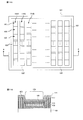
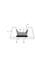
第1バンクは、後述する有機層が塗布される領域を規定する基板上に配置された障壁である。第1バンクは基板上にライン状に複数本形成され、基板上にライン状の領域を規定する(図6A参照)。ライン状の領域には、後述する有機層が塗布される。以下、ライン状のバンク(第1バンク)によって規定されるライン状の領域を「塗布領域」と称する。第1バンクによって規定された1の塗布領域内には、画素領域が1列に並んでいる(図6A参照)。ここで、画素領域とは一つの有機EL素子が占める領域を意味する。
ライン状の第1バンクは互いに並行であることが好ましい。また、画素電極がライン状に形成される場合(パッシブマトリックス型有機ELディスプレイパネルの場合)、ライン状の第1バンクのラインの方向と、画素電極のラインの方向とは直交することが好ましい。 About First Bank The first bank is a barrier disposed on a substrate that defines a region to which an organic layer described later is to be applied. A plurality of first banks are formed in a line on the substrate, and a line area is defined on the substrate (see FIG. 6A). An organic layer described later is applied to the linear region. Hereinafter, a linear area defined by the linear bank (first bank) will be referred to as a "coating area". Pixel regions are arranged in a line in one application region defined by the first bank (see FIG. 6A). Here, the pixel area means an area occupied by one organic EL element.
The linear first banks are preferably parallel to one another. When the pixel electrode is formed in a line (in the case of a passive matrix organic EL display panel), it is preferable that the direction of the line of the first bank and the direction of the line of the pixel electrode be orthogonal to each other.

例えば、厚さ1μmのフッ素含有樹脂膜の表面におけるフッ素原子濃度は、7.5atom%であり、フッ素含有樹脂膜の表面における水接触角は81.2°であり、フッ素含有樹脂膜の表面におけるアニソールの接触角は45.5°である。
また、厚さが0.3μmのフッ素含有樹脂膜の表面におけるフッ素原子濃度は、3.0atom%であり、フッ素含有樹脂膜の表面における水接触角は64.6°であり、フッ素含有樹脂膜の表面におけるアニソールの接触角は28.4°である。 As shown in Table 1, the thicker (higher) the fluorine-containing resin film, the higher the fluorine concentration on the surface of the fluorine-containing resin film. Since the wettability of the fluorine-containing resin is mainly determined by the concentration of the fluorine atom, the higher the fluorine concentration, the larger the contact angle of water and the contact angle of the organic solvent (the wettability decreases).
For example, the fluorine atom concentration at the surface of the fluorine-containing resin film having a thickness of 1 μm is 7.5 atom%, the water contact angle at the surface of the fluorine-containing resin film is 81.2 °, and the surface at the surface of the fluorine-containing resin film The contact angle of anisole is 45.5 °.
The fluorine atom concentration on the surface of the fluorine-containing resin film having a thickness of 0.3 μm is 3.0 atom%, the water contact angle on the surface of the fluorine-containing resin film is 64.6 °, and the fluorine-containing resin film The contact angle of anisole on the surface of is 28.4 °.
第2バンクは、基板上に配置され、塗布領域内に2以上の画素領域を規定(図6参照)し、塗布領域内を平坦にするための機能を有する。本発明では、塗布法によって形成される有機層は、第2バンク上にも配置されることから、第2バンクの高さは第1バンクよりも低い。第2バンクの高さについては後述する。 About Second Bank The second bank is disposed on the substrate, defines two or more pixel areas in the application area (see FIG. 6), and has a function to flatten the inside of the application area. In the present invention, since the organic layer formed by the coating method is also disposed on the second bank, the height of the second bank is smaller than that of the first bank. The height of the second bank will be described later.
第1バンクの材料と第2バンクの材料とが異なる場合、第2バンクの材料に、第1バンクよりも濡れ性の高い樹脂を用いればよい。濡れ性の高い樹脂の例には、フッ素を含有しないポリイミド樹脂やアクリル樹脂などが含まれる。 A) When the material of the first bank and the material of the second bank are different When the material of the first bank and the material of the second bank are different, the material of the second bank is a resin having higher wettability than the first bank Should be used. Examples of highly wettable resins include polyimide resins and acrylic resins that do not contain fluorine.
第1バンクの材料と第2バンクの材料とが同じであるにもかかわらず、第1バンクの上面の濡れ性を低くし、第2バンクの上面の濡れ性を高くするには、第1バンクおよび第2バンクの材料を共にフッ素含有樹脂とすればよい。 B) When the material of the first bank and the material of the second bank are the same: Even though the material of the first bank and the material of the second bank are the same, lower the wettability of the top surface of the first bank, In order to increase the wettability of the upper surface of the second bank, both the materials of the first bank and the second bank may be made of a fluorine-containing resin.
第2バンクの高さは、後述する有機層の底面と接する層(以下単に「有機層の下層」とも称する)の素材によって異なる。上述したように、本発明では、i)画素電極上に直接有機層が配置される場合と、ii)遷移金属の酸化物からなる正孔注入層上に有機層が配置される場合と、iii)PEDOT-PSSを含む正孔注入層上に有機層が配置される場合とがある。このため、有機層の下層は、i)画素電極である場合と、ii)遷移金属の酸化物からなる正孔注入層である場合と、iii)PEDOT-PSSを含む正孔注入層である場合と、がある。以下、第2バンクの高さについて、それぞれの場合に分けて説明する。 About the height of the second bank The height of the second bank differs depending on the material of the layer in contact with the bottom surface of the organic layer described below (hereinafter, also simply referred to as "the lower layer of the organic layer"). As described above, in the present invention, i) the case where the organic layer is disposed directly on the pixel electrode, ii) the case where the organic layer is disposed on the hole injection layer made of the transition metal oxide, and iii The organic layer may be disposed on the hole injection layer containing PEDOT-PSS. Therefore, the lower layer of the organic layer is i) a pixel electrode, ii) a hole injection layer made of transition metal oxide, and iii) a hole injection layer containing PEDOT-PSS. There is. Hereinafter, the height of the second bank will be described separately for each case.
有機層の下層が画素電極である場合、第2バンクの画素電極の表面からの高さは-0.1~+0.4μmであることが好ましく、約0μmであることがさらに好ましい。このように、有機層の下層が画素電極である場合、第2バンクは塗布法で形成される層を規定する必要がないので、第2バンクの画素電極の表面からの高さを比較的低くすることができる。これにより塗布領域内を平坦にすることができ、有機層の膜厚をより均一にすることができる。 i) When the lower layer of the organic layer is a pixel electrode When the lower layer of the organic layer is a pixel electrode, the height from the surface of the pixel electrode of the second bank is preferably −0.1 to +0.4 μm, More preferably, it is about 0 μm. As described above, when the lower layer of the organic layer is the pixel electrode, the second bank does not have to define the layer formed by the coating method, so the height from the surface of the pixel electrode of the second bank is relatively low. can do. Thereby, the inside of the application region can be made flat, and the film thickness of the organic layer can be made more uniform.
有機層の下層が遷移金属の酸化物からなる正孔注入層である場合、第2バンクの遷移金属の酸化物からなる正孔注入層の表面からの高さは-0.1~+0.4μmであることが好ましく、約0μmであることがさらに好ましい。このように、有機層の下層が遷移金属の酸化物からなる正孔注入層である場合、第2バンクは塗布法で形成される層を規定する必要がないので、第2バンクの遷移金属の酸化物からなる正孔注入層の表面からの高さを比較的低くすることができる。これにより塗布領域内を平坦にすることができ、有機層の膜厚をより均一にすることができる。 ii) In the case where the lower layer of the organic layer is a hole injection layer composed of a transition metal oxide (see Embodiment 1)
When the lower layer of the organic layer is a hole injection layer made of a transition metal oxide, the height from the surface of the hole injection layer made of a transition metal oxide of the second bank is -0.1 to +0.4 μm Is preferably, and more preferably about 0 μm. As described above, when the lower layer of the organic layer is a hole injection layer made of a transition metal oxide, the second bank does not have to define the layer formed by the coating method. The height from the surface of the hole injection layer made of oxide can be made relatively low. Thereby, the inside of the application region can be made flat, and the film thickness of the organic layer can be made more uniform.
有機層の下層が遷移金属の酸化物からなる正孔注入層である場合、第2バンクの画素電極の表面からの高さは0.1~0.5μmであることが好ましい。PEDOT-PSSを含む正孔注入層は塗布法で形成される。このため有機層の下層がPEDOT-PSSを含む正孔注入層である場合、第2バンクは、正孔注入層の材料液(PEDOT-PSSと水を含む溶液)が塗布される領域を規定することが要求される。このため、i)およびii)と比較して第2バンクのPEDOT-PSSを含む正孔注入層の表面からの高さが高くなる。 iii) The lower layer of the organic layer is a hole injection layer containing PEDOT-PSS (see Embodiment 2)
When the lower layer of the organic layer is a hole injection layer composed of a transition metal oxide, the height from the surface of the pixel electrode of the second bank is preferably 0.1 to 0.5 μm. The hole injection layer containing PEDOT-PSS is formed by a coating method. Therefore, when the lower layer of the organic layer is a hole injection layer containing PEDOT-PSS, the second bank defines a region to which the material liquid of the hole injection layer (a solution containing PEDOT-PSS and water) is applied. Is required. For this reason, the height from the surface of the hole injection layer including PEDOT-PSS of the second bank is increased compared to i) and ii).
有機層は、少なくとも有機発光層を含み、画素電極上に配置された層である。有機層は、第1バンクによって規定されるライン状塗布領域に有機層の材料液を塗布することで形成される。有機層の材料液(有機層の材料をアニソールやシクロベンゼンなどの有機溶媒に溶解したインク)を、インクジェットなどの塗布法によって後述する塗布領域に塗布することによって、容易かつ他の材料に損傷を与えることなく有機層を形成することができるからである。本発明では、有機層は後述する第1バンクによって規定された塗布領域にライン状に(複数の有機EL素子に亘って)形成される。このため、有機層は、画素領域上だけでなく第2バンク上にも配置される。 4) Organic Layer The organic layer is a layer including at least an organic light emitting layer and disposed on the pixel electrode. The organic layer is formed by applying the material solution of the organic layer to the linear application region defined by the first bank. By applying the material solution of the organic layer (ink in which the material of the organic layer is dissolved in an organic solvent such as anisole or cyclobenzene) to a coating region described later by a coating method such as inkjet, damage to other materials is easy It is because an organic layer can be formed without giving. In the present invention, the organic layer is formed in a line shape (across a plurality of organic EL elements) in the application region defined by the first bank described later. Therefore, the organic layer is disposed not only on the pixel region but also on the second bank.
対向電極とは、有機層上に配置された導電性部材である。有機ELディスプレイパネルでは、対向電極は通常、陰極として機能するが、陽極としても機能しうる。対向電極の材料は、ボトムエミッション型か、トップエミッション型かによってその材料が異なる。トップエミッション型の場合には、対向電極が透明である必要があるので、対向電極の材料はITO電極やIZO電極などであることが好ましい。対向電極の材料は、Ba、Al、WOxなどであってもよい。さらに、トップエミッション型の場合、有機発光層と対向電極層との間に有機バッファー層を配置してもよい。 5) Counter electrode The counter electrode is a conductive member disposed on the organic layer. In the organic EL display panel, the counter electrode usually functions as a cathode but can also function as an anode. The material of the counter electrode differs depending on whether it is bottom emission type or top emission type. In the case of the top emission type, since the counter electrode needs to be transparent, the material of the counter electrode is preferably an ITO electrode, an IZO electrode, or the like. The material of the counter electrode may be Ba, Al, WOx or the like. Furthermore, in the case of top emission type, an organic buffer layer may be disposed between the organic light emitting layer and the counter electrode layer.
本発明の有機ELディスプレイパネルは、本発明の効果を損なわない限り、任意の方法で製造され得る。 2. About the manufacturing method of the organic electroluminescent display panel of this invention The organic electroluminescent display panel of this invention may be manufactured by arbitrary methods, as long as the effect of this invention is not impaired.
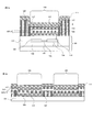
1)画素電極が配置された基板を準備する第1ステップ(図3A)と、
2)基板上に第1バンクおよび第2バンクを形成する第2ステップ(図3B)と、
3)塗布領域にライン状の有機層を形成する第3ステップ(図3C、図3D)と、
4)有機層上に対向電極を形成する第4ステップ(図3E)と、を含む。以下図面を参照して本発明のアクティブマトリクス型の有機ELディスプレイパネルの好ましい製造方法について説明する。 An example of a preferred manufacturing method is
1) a first step (FIG. 3A) of preparing a substrate on which a pixel electrode is disposed;
2) a second step (FIG. 3B) of forming a first bank and a second bank on the substrate;
3) Third step (FIGS. 3C and 3D) of forming a line-shaped organic layer in the application area;
4) forming a counter electrode on the organic layer (FIG. 3E). Hereinafter, a preferred method of manufacturing the active matrix organic EL display panel of the present invention will be described with reference to the drawings.
画素電極103は、例えば、スパッタリング法などにより、電極材料の膜を基板101上に形成し、エッチングしてパターニングすることにより形成される。また、画素電極103上に遷移金属の酸化物からなる正孔注入層を形成してもよい。 1) FIG. 3A shows the first step. In the first step, the
The
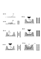
本発明では、第1バンク105および第2バンク107を形成するステップは、樹脂膜をパターニングするステップと、パターニングされた樹脂膜をベークするステップとを有する。樹脂膜はフォトリソグラフィ法でパターニングされうる。また樹脂膜は、凹版印刷などによってパターニングされてもよい。凹版印刷などで形成すれば、他の材料(画素電極など)に損傷を与えにくい。また、樹脂膜は、凸版印刷によってパターニングしてもよい。 2) FIG. 3B shows the second step. In the second step, the
In the present invention, the step of forming the
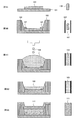
i)基板上に、感光性樹脂膜Aを形成するステップi(図4A)と、
ii)感光性樹脂膜A上に感光性樹脂膜Bを形成するステップii(図4B)と、
iii)感光性樹脂膜Aおよび感光性樹脂膜Bを透過率の異なるハーフトーンマスクを介して露光し、現像するステップiii(図4C、図4D)と、を有する。 In the step of patterning a resin film by photolithography,
i) Step i (FIG. 4A) of forming a photosensitive resin film A on a substrate;
ii) forming a photosensitive resin film B on the photosensitive resin film A (FIG. 4B);
iii) exposing and developing the photosensitive resin film A and the photosensitive resin film B through halftone masks having different transmittances, as shown in FIG. 4C and FIG. 4D.
i)基板上に、感光性樹脂膜104’を形成するステップi(図5A)と、
ii)感光性樹脂膜104’を透過率の異なるハーフトーンマスク110を介して露光し、現像するステップii(図5B、図5C)と、を有していてもよい。 Also, the step of patterning the resin film by photolithography is as shown in FIGS. 5A to 5C,
i) forming a photosensitive resin film 104 'on a substrate (FIG. 5A);
ii) Step ii (FIGS. 5B and 5C) of exposing and developing the
実施の形態1では、トップエミッション型有機ELディスプレイパネルについて説明する。また、実施の形態1の有機ELディスプレイパネルはアクティブマトリクス型である。
In the first embodiment, a top emission type organic EL display panel will be described. Moreover, the organic EL display panel of
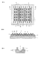
図6Aおよび図6Bに示されるように、実施の形態1の有機ELディスプレイパネルでは、基板101上に複数のライン状の第1バンク105が配置されている。第1バンク105は塗布領域119を規定している。塗布領域119は、レッドの光を発光する塗布領域119R;グリーンの光を発光する塗布領域119G;ブルーの光を発光する塗布領域119Bに分類され、順番に配置されている。また、基板101上には第1バンク105よりも低い第2バンク107が配置されている。第2バンク107は塗布領域119内に配列された複数の画素領域120を規定する。本実施の形態では塗布領域119の長軸方向の端部はバンクによって規定されない。 FIG. 6A is a plan view of the active matrix organic EL display panel according to
As shown in FIGS. 6A and 6B, in the organic EL display panel according to the first embodiment, a plurality of line-shaped
第2バンク107は、上述のように画素領域120を規定する。また、本実施の形態では、第2バンク107の正孔注入層113の表面からの高さ107hは、-0.1~+0.4μmである。 The
The
実施の形態1では、正孔注入層が遷移金属の酸化物からなる例について説明した。実施の形態2では、正孔注入層がPEDOT-PSSを含む例について説明する。 Second Embodiment
In the first embodiment, the example in which the hole injection layer is made of a transition metal oxide has been described. In Embodiment 2, an example in which the hole injection layer includes PEDOT-PSS will be described.
正孔注入層113’は、PEDOT-PSSを含む。後述するように、正孔注入層113’はPEDOT-PSSを含む水溶液を第2バンク107によって規定された領域内に塗布することで形成される。このように、塗布法で形成される正孔注入層113’は、画素領域120(有機EL素子)ごとに独立して配置される。 1) Hole injection layer 113 '
The
R=ρL/A
R:抵抗 ρ:PEDOT-PSSの比抵抗
L:画素電極間の距離
A:正孔注入層(PEDOT-PSS)の断面積 [Equation 1]
R = ρL / A
R: Resistance ρ: PEDOT-PSS specific resistance
L: Distance between pixel electrodes A: Cross section of hole injection layer (PEDOT-PSS)
本実施の形態では、第2バンク107は、塗布領域119内の画素領域120を規定し、塗布法で形成される正孔注入層113’の配置領域を規定する障壁である。また、第2バンク107の上面の濡れ性は、第1バンク105の上面の濡れ性よりも高い。 2)
In the present embodiment, the
一方、第2バンク107上には、ライン状の有機層(電子ブロック層115)が塗布法によって形成されることから、第2バンク107の上面は、電子ブロック層115の材料液(電子ブロック層115の材料とアニソールなどの有機溶媒を含む溶液)に対しては親液性を示すことが要求される。 As described above, since the
On the other hand, since the linear organic layer (electron block layer 115) is formed by the coating method on the
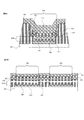
1)基板101を準備する第1ステップ(図10A)、
2)基板101上に画素電極103を配置する第2ステップ(図10B)
3)塗布領域を規定するライン状の第1バンク105と画素領域を規定する第2バンク107を形成する第3ステップ(図10C)、
4)第2バンク107によって規定された画素領域に正孔注入層を形成する第4ステップ(図10D)、
5)第1バンク105によって規定されたライン状の塗布領域にライン状の電子ブロック層を形成する第5ステップ(図10E)、
6)塗布領域内の電子ブロック層上にライン状の有機発光層を形成する第6ステップ(図10F)、
7)有機発光層上に対向電極を形成する第7ステップ(図10G)、を有する。以下それぞれのステップについて説明する。 The manufacturing method of the organic EL display panel of Embodiment 2 is
1) a first step of preparing the substrate 101 (FIG. 10A),
2) Second step of arranging the
3) forming a linear
4) forming a hole injection layer in the pixel area defined by the second bank 107 (FIG. 10D);
5) a fifth step (FIG. 10E) of forming a linear electron block layer in the linear application region defined by the
6) a sixth step (FIG. 10F) of forming a linear organic light emitting layer on the electron blocking layer in the application region;
7) A seventh step (FIG. 10G) of forming a counter electrode on the organic light emitting layer. Each step will be described below.
実施の形態1および2では塗布領域の長軸方向の端部が規定されていない例について説明した。本実施の形態では塗布領域の長軸方向の端部も第1バンクによって規定されている例について説明する。また、実施の形態1および実施の形態2では、画素領域と、第1バンクとの間に第2バンクが配置される形態について説明したが(図6参照)、実施の形態3では、画素領域と、第1バンクとの間に第2バンクが配置されない形態について説明する。 Third Embodiment
In
その後、反射画素電極がパターニングされたガラス基板上に感光性のフッ素化合物を含むアクリル系樹脂の塗布膜(厚さ:1.0μm)を形成した。次に、塗布膜をハーフトーンマスクを介して露光し、第1バンク(高さ1.0μm)および第2バンク(高さ0.1~0.3μm)をパターニングし、ベーク処理(220℃、1時間)を行い、第1バンクおよび第2バンクを形成した。 An APC film with a thickness of 100 to 200 nm was formed by sputtering on a φ6 inch glass substrate, and etching was performed using a resist as a mask to pattern a reflective pixel electrode.
After that, a coating film (thickness: 1.0 μm) of an acrylic resin containing a photosensitive fluorine compound was formed on the glass substrate on which the reflective pixel electrode was patterned. Next, the coated film is exposed through a halftone mask, and the first bank (height 1.0 μm) and the second bank (height 0.1 to 0.3 μm) are patterned and baked (220 ° C., 1 hour was performed to form the first bank and the second bank.
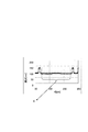
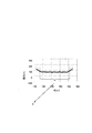
本実施例では、画素領域内における有機発光層の膜厚は、±3%の範囲でばらついた。 The graph of FIG. 13 shows the results of the film thickness distribution measurement of the example. The vertical axis of the graph of FIG. 13 indicates the thickness of the organic light emitting layer. The horizontal axis of the graph of FIG. 13 indicates the measurement position. Further, A in the graph of FIG. 13 indicates the length of the pixel area in the X direction.
In the present embodiment, the film thickness of the organic light emitting layer in the pixel region was dispersed in the range of ± 3%.
比較例では、第2バンクの高さを第1バンクの高さ(1.0μm)と同じにした以外は、実施例と同じ方法で有機ELディスプレイパネルのモデルを形成した。すなわち比較例では、同じ高さのバンクが画素領域の四方を囲む。また、実施例では、正孔注入層が有機EL素子ごとに独立して配置され、電子ブロック層および有機発光層はライン状に形成されるのに対し、比較例では、正孔注入層、電子ブロック層および有機発光層のいずれもが有機EL素子ごとに配置される。
比較例の有機ELディスプレイモデルは、図14に示すように画素領域を規定するバンク17のみを有する。また、図14の線A-A’の断面図における有機EL素子は図15のような構造を示す。 (Comparative example)
In the comparative example, a model of the organic EL display panel was formed in the same manner as the example except that the height of the second bank was made the same as the height (1.0 μm) of the first bank. That is, in the comparative example, banks of the same height surround four sides of the pixel area. In the example, the hole injection layer is disposed independently for each organic EL element, and the electron blocking layer and the organic light emitting layer are formed in a line shape, while in the comparative example, the hole injection layer, the electron Both the block layer and the organic light emitting layer are disposed for each organic EL element.
The organic EL display model of the comparative example has only a
2 第1の電極層
3 第2バンク
4 第1バンク
5 正孔注入層
6 有機発光層
30 画素領域
40 ライン状領域
17 バンク
101 基板
103 画素電極
104 感光性樹脂膜A
105、105’ 第1バンク
106 感光性樹脂膜B
107 第2バンク
109 有機層
111 対向電極
113、113’ 正孔注入層
110 ハーフトーンマスク
115 電子ブロック層
117 有機発光層
118 電子注入層
119 塗布領域
120 画素領域
131 ゲート電極
132 ゲート絶縁膜
133 ソース電極
134 ドレイン電極
135 半導体層
136 コンタクトホール REFERENCE SIGNS
105, 105 '
107
Claims (14)
- 基板と、
前記基板上に配置され、ライン状の領域を規定するライン状の第1バンクと、
前記ライン状の領域内に配列された2以上の画素領域を規定する第2バンクと、
前記画素領域に配置された画素電極と、
前記ライン状の領域内に配置され、前記画素領域および前記第2バンク上に塗布法によって形成されたライン状の有機層と、
前記有機層上に配置された対向電極と、を含む有機ELディスプレイパネルであって、
前記第1バンクの高さは、前記第2バンクの高さよりも高く、
前記第1バンクおよび第2バンクの材料は樹脂であり、
前記第1バンクの頂点におけるアニソールの接触角は、30°~60°であり、
前記第2バンクの頂点におけるアニソールの接触角は、5°~30°である、有機ELディスプレイパネル。 A substrate,
A line-shaped first bank disposed on the substrate and defining a line-shaped area;
A second bank defining two or more pixel areas arranged in the linear area;
A pixel electrode disposed in the pixel area;
A line-shaped organic layer disposed in the line-shaped area and formed on the pixel area and the second bank by a coating method;
And an opposing electrode disposed on the organic layer.
The height of the first bank is higher than the height of the second bank,
The material of the first and second banks is a resin,
The contact angle of anisole at the top of said first bank is between 30 ° and 60 °,
The organic EL display panel, wherein the contact angle of anisole at the top of the second bank is 5 ° to 30 °. - 前記第1バンクの前記基板の表面からの高さは0.5~3μmである、請求項1に記載の有機ELディスプレイパネル。 The organic EL display panel according to claim 1, wherein the height from the surface of the substrate of the first bank is 0.5 to 3 μm.
- 前記有機層の底面は、前記画素電極と接触し、
前記画素電極の表面からの前記第2バンクの高さは、-0.1~+0.4μmである、請求項1に記載の有機ELディスプレイパネル。 The bottom surface of the organic layer is in contact with the pixel electrode,
The organic EL display panel according to claim 1, wherein the height of the second bank from the surface of the pixel electrode is -0.1 to +0.4 μm. - 前記画素電極上に配置され、前記画素領域ごとに独立した正孔注入層をさらに有し、
前記有機層の底面は、前記正孔注入層と接触する、請求項1に記載の有機ELディスプレイパネル。 It further comprises a hole injection layer disposed on the pixel electrode and independent for each of the pixel regions,
The organic EL display panel according to claim 1, wherein a bottom surface of the organic layer is in contact with the hole injection layer. - 前記正孔注入層は、遷移金属の酸化物を含み、
前記正孔注入層の表面からの前記第2バンクの高さは、-0.1~+0.4μmである、請求項4に記載の有機ELディスプレイパネル。 The hole injection layer comprises an oxide of a transition metal,
5. The organic EL display panel according to claim 4, wherein the height of the second bank from the surface of the hole injection layer is −0.1 to +0.4 μm. - 前記正孔注入層は、ポリエチレンジオキシチオフェンを含み、
前記画素電極の表面からの前記第2バンクの高さは、0.1~0.5μmである、請求項4に記載の有機ELディスプレイパネル。 The hole injection layer comprises polyethylenedioxythiophene.
5. The organic EL display panel according to claim 4, wherein the height of the second bank from the surface of the pixel electrode is 0.1 to 0.5 μm. - 前記第1バンクの材料は、フッ素含有樹脂である、請求項1に記載の有機ELディスプレイパネル。 The organic EL display panel according to claim 1, wherein the material of the first bank is a fluorine-containing resin.
- 前記第1バンクは、前記第1バンクの高さ方向に沿ってフッ素濃度の勾配を有し、
前記第1バンクの頂点におけるフッ素濃度は、前記第1バンクの底面におけるフッ素濃度よりも高い、請求項7に記載の有機ELディスプレイパネル。 The first bank has a fluorine concentration gradient along the height direction of the first bank,
The organic EL display panel according to claim 7, wherein the fluorine concentration at the top of the first bank is higher than the fluorine concentration at the bottom of the first bank. - 前記第2バンクの材料は、フッ素含有樹脂である、請求項7に記載の有機ELディスプレイパネル。 The organic EL display panel according to claim 7, wherein the material of the second bank is a fluorine-containing resin.
- 前記第1バンクの頂点におけるフッ素濃度は、前記第2バンクの頂点におけるフッ素濃度よりも高い、請求項9に記載の有機ELディスプレイパネル。 The organic EL display panel according to claim 9, wherein the fluorine concentration at the top of the first bank is higher than the fluorine concentration at the top of the second bank.
- 画素電極が配置された基板を準備するステップと、
前記基板上にライン状の領域を規定するライン状の第1バンクと、前記ライン状の領域内に配列された2以上の画素領域を規定する第2バンクと、を形成するステップと、
前記ライン状の領域に有機EL材料を含む材料液を塗布し、ライン状の有機層を形成するステップと、
前記有機層上に対向電極を形成するステップと、を有し、
前記第1バンクの高さは、前記第2バンクの高さよりも高く、
前記第1バンクおよび第2バンクの材料は樹脂であり、
前記第1バンクの頂点におけるアニソールの接触角は、30°~60°であり、
前記第2バンクの頂点におけるアニソールの接触角は、5°~30°である、有機ELディスプレイパネルの製造方法。 Preparing a substrate on which the pixel electrode is disposed;
Forming a first linear bank defining a linear region on the substrate and a second bank defining two or more pixel regions arranged in the linear region;
Applying a material liquid containing an organic EL material to the linear region to form a linear organic layer;
Forming a counter electrode on the organic layer;
The height of the first bank is higher than the height of the second bank,
The material of the first and second banks is a resin,
The contact angle of anisole at the top of said first bank is between 30 ° and 60 °,
The method of manufacturing an organic EL display panel, wherein the contact angle of anisole at the top of the second bank is 5 ° to 30 °. - 前記第1バンクおよび前記第2バンクを形成するステップは、
前記基板上に、樹脂膜をパターニングするステップと、
前記樹脂膜をベークするステップと、
を有する、請求項11に記載の有機ELディスプレイパネルの製造方法。 The steps of forming the first bank and the second bank include:
Patterning a resin film on the substrate;
Baking the resin film;
The manufacturing method of the organic electroluminescent display panel of Claim 11 which has these. - 前記樹脂膜をパターニングするステップは、
前記基板上に、前記第2バンクの材料を含む感光性樹脂膜Aを形成するステップと、
前記感光性樹脂膜A上に前記第1バンクの材料を含み、前記感光性樹脂膜Aとは感度の異なる感光性樹脂膜Bを形成するステップと、
前記感光性樹脂膜Aおよび前記感光性樹脂膜Bを透過率の異なるマスクを介して露光し、現像するステップと、を有する請求項12に記載の有機ELディスプレイパネルの製造方法。 In the step of patterning the resin film,
Forming a photosensitive resin film A containing the material of the second bank on the substrate;
Forming a photosensitive resin film B containing a material of the first bank on the photosensitive resin film A and having a sensitivity different from that of the photosensitive resin film A;
And exposing the photosensitive resin film A and the photosensitive resin film B through masks having different transmittances, and developing the photosensitive resin film B and the photosensitive resin film B. - 前記樹脂膜をパターニングするステップは、
前記基板上に、フッ素化合物を含む感光性樹脂膜を形成するステップと、
前記フッ素化合物を含む感光性樹脂膜を透過率の異なるハーフトーンマスクを介して露光し、現像するステップと、を有する請求項12に記載の有機ELディスプレイパネルの製造方法。
In the step of patterning the resin film,
Forming a photosensitive resin film containing a fluorine compound on the substrate;
And exposing the photosensitive resin film containing the fluorine compound through a halftone mask having different transmittances, and developing the photosensitive resin film.
Priority Applications (5)
| Application Number | Priority Date | Filing Date | Title |
|---|---|---|---|
| CN2009800005549A CN101689559B (en) | 2008-06-06 | 2009-06-02 | Organic el display panel and manufacturing method thereof |
| JP2009545019A JP4495781B2 (en) | 2008-06-06 | 2009-06-02 | Organic EL display panel and manufacturing method thereof |
| EP09758105.2A EP2242334B1 (en) | 2008-06-06 | 2009-06-02 | Organic el display panel and manufacturing method thereof |
| KR1020097026813A KR100984574B1 (en) | 2008-06-06 | 2009-06-02 | Organic EL display panel and its manufacturing method |
| US12/669,094 US7842947B2 (en) | 2008-06-06 | 2009-06-02 | Organic EL display panel and manufacturing method thereof |
Applications Claiming Priority (2)
| Application Number | Priority Date | Filing Date | Title |
|---|---|---|---|
| JP2008-149388 | 2008-06-06 | ||
| JP2008149388 | 2008-06-06 |
Publications (1)
| Publication Number | Publication Date |
|---|---|
| WO2009147838A1 true WO2009147838A1 (en) | 2009-12-10 |
Family
ID=41397921
Family Applications (1)
| Application Number | Title | Priority Date | Filing Date |
|---|---|---|---|
| PCT/JP2009/002475 WO2009147838A1 (en) | 2008-06-06 | 2009-06-02 | Organic el display panel and manufacturing method thereof |
Country Status (6)
| Country | Link |
|---|---|
| US (1) | US7842947B2 (en) |
| EP (1) | EP2242334B1 (en) |
| JP (1) | JP4495781B2 (en) |
| KR (1) | KR100984574B1 (en) |
| CN (1) | CN101689559B (en) |
| WO (1) | WO2009147838A1 (en) |
Cited By (18)
| Publication number | Priority date | Publication date | Assignee | Title |
|---|---|---|---|---|
| JP2010073700A (en) * | 2007-12-28 | 2010-04-02 | Panasonic Corp | Organic el device and organic el display panel |
| JP2011103222A (en) * | 2009-11-11 | 2011-05-26 | Seiko Epson Corp | Organic el element, method of manufacturing the same, organic el device, and electronic equipment |
| JP2011141446A (en) * | 2010-01-07 | 2011-07-21 | Seiko Epson Corp | Substrate for electrooptical device and method for manufacturing the same, electrooptical device, and electronic apparatus |
| KR101084193B1 (en) | 2010-02-16 | 2011-11-17 | 삼성모바일디스플레이주식회사 | An organic light emitting display device and the manufacturing method thereof |
| JP2012216495A (en) * | 2011-03-30 | 2012-11-08 | Sony Corp | Organic light emitting element and display device including the same |
| EP2563097A1 (en) * | 2010-04-19 | 2013-02-27 | Panasonic Corporation | Organic el display panel and organic el display device equipped with same, and production method for organic el display panel |
| JP2013041828A (en) * | 2011-08-12 | 2013-02-28 | Samsung Display Co Ltd | Organic light emitting element and method of manufacturing the same |
| JPWO2013093974A1 (en) * | 2011-12-22 | 2015-04-27 | パナソニック株式会社 | Organic EL display panel |
| JP2016091841A (en) * | 2014-11-06 | 2016-05-23 | 株式会社Joled | Organic light-emitting device and organic display device |
| CN106129264A (en) * | 2016-07-21 | 2016-11-16 | 深圳市华星光电技术有限公司 | Pixel defines the manufacture method of layer and the manufacture method of OLED |
| CN106206970A (en) * | 2016-08-31 | 2016-12-07 | 深圳市华星光电技术有限公司 | A kind of luminescent panel and preparation method thereof |
| CN106505159A (en) * | 2016-11-14 | 2017-03-15 | 深圳市华星光电技术有限公司 | Manufacture method for printing the groove structure and OLED display device of OLED display device |
| CN106935735A (en) * | 2017-05-12 | 2017-07-07 | 京东方科技集团股份有限公司 | The preparation method of display base plate, display base plate and display device |
| US10109691B2 (en) | 2014-06-25 | 2018-10-23 | Joled Inc. | Method for manufacturing organic EL display panel |
| JP2020095961A (en) * | 2018-12-14 | 2020-06-18 | エルジー ディスプレイ カンパニー リミテッド | Electroluminescent display device and method of manufacturing the same |
| WO2022163472A1 (en) * | 2021-01-29 | 2022-08-04 | 富士フイルム株式会社 | Sensor cover and sensor |
| KR20220119011A (en) | 2019-12-20 | 2022-08-26 | 미쯔비시 케미컬 주식회사 | Photosensitive resin composition, barrier rib, organic electroluminescent element, and image display device |
| WO2023145055A1 (en) * | 2022-01-31 | 2023-08-03 | シャープディスプレイテクノロジー株式会社 | Light-emitting device and production method therefor |
Families Citing this family (68)
| Publication number | Priority date | Publication date | Assignee | Title |
|---|---|---|---|---|
| EP2141964B1 (en) * | 2007-05-31 | 2011-09-07 | Panasonic Corporation | Organic EL element and manufacturing method thereof |
| JP4612741B2 (en) * | 2008-08-29 | 2011-01-12 | パナソニック株式会社 | Organic EL display panel and manufacturing method thereof |
| JP5209123B2 (en) | 2009-11-04 | 2013-06-12 | パナソニック株式会社 | Display panel device and manufacturing method thereof |
| WO2012017495A1 (en) | 2010-08-06 | 2012-02-09 | パナソニック株式会社 | Organic el element and production method for same |
| WO2012017489A1 (en) * | 2010-08-06 | 2012-02-09 | パナソニック株式会社 | Organic el element, display device, and light-emitting device |
| JP5677434B2 (en) * | 2010-08-06 | 2015-02-25 | パナソニック株式会社 | Organic EL device |
| WO2012017496A1 (en) | 2010-08-06 | 2012-02-09 | パナソニック株式会社 | Light emitting device, light emitting apparatus provided with a light emitting device, and method of manufacturing a light emitting device |
| CN103038908B (en) | 2010-08-06 | 2016-01-06 | 株式会社日本有机雷特显示器 | Light-emitting component, possess the light-emitting device of light-emitting component and the manufacture method of light-emitting component |
| WO2012025954A1 (en) | 2010-08-25 | 2012-03-01 | パナソニック株式会社 | Organic light-emitting element and process for production thereof, and organic display panel and organic display device |
| WO2012025961A1 (en) * | 2010-08-25 | 2012-03-01 | パナソニック株式会社 | Organic light emitting element, method for producing same, organic display panel, and organic display device |
| WO2012073270A1 (en) * | 2010-11-29 | 2012-06-07 | パナソニック株式会社 | Method of producing organic light-emitting diode, organic light-emitting diode, luminescent device, display panel, and display device |
| WO2012098587A1 (en) | 2011-01-21 | 2012-07-26 | パナソニック株式会社 | Organic el element |
| KR101784994B1 (en) * | 2011-03-31 | 2017-10-13 | 삼성디스플레이 주식회사 | Organic light emitting diode display and manufacturing method thereof |
| CN102960068B (en) * | 2011-04-22 | 2015-12-23 | 株式会社日本有机雷特显示器 | Organic EL display panel and manufacture method thereof |
| TW201403905A (en) * | 2012-06-01 | 2014-01-16 | Sony Corp | Organic electroluminescence device, manufacturing method thereof, and electronic equipment |
| JP6159977B2 (en) * | 2012-08-23 | 2017-07-12 | 株式会社Joled | Method for manufacturing organic electronic device and method for manufacturing organic EL device |
| KR101970540B1 (en) * | 2012-11-15 | 2019-08-14 | 삼성디스플레이 주식회사 | Organic light emitting display device and method for fabricting the same |
| KR20140070142A (en) | 2012-11-30 | 2014-06-10 | 삼성디스플레이 주식회사 | Organic light emitting display and manufacturing method thereof |
| KR102046157B1 (en) * | 2012-12-21 | 2019-12-03 | 삼성디스플레이 주식회사 | Organic light emitting diode display and manufacturing method thereof |
| JP6174877B2 (en) * | 2013-03-21 | 2017-08-02 | 株式会社半導体エネルギー研究所 | Display device and electronic device |
| KR102024696B1 (en) * | 2013-03-22 | 2019-09-25 | 삼성디스플레이 주식회사 | Organic light emitting diode, organic light emitting display panel having the organic light emitting diode and fabricating method for the organic light emitting display panel |
| KR102099702B1 (en) * | 2013-05-16 | 2020-04-13 | 삼성디스플레이 주식회사 | Organic light emitting display device and method of manufacturing having the same |
| KR102114314B1 (en) * | 2013-06-26 | 2020-05-25 | 삼성디스플레이 주식회사 | Organic light emitting display device and method for manufacturing the same |
| TWI566353B (en) | 2013-08-21 | 2017-01-11 | 精材科技股份有限公司 | Semiconductor structure and manufacturing method thereof |
| KR102083982B1 (en) | 2013-10-29 | 2020-04-16 | 삼성디스플레이 주식회사 | Organic light emitting device and manufacturing method thereof |
| TWI467528B (en) * | 2013-10-30 | 2015-01-01 | Au Optronics Corp | Light emitting diode display panel and method of fabricating the same |
| US9997575B2 (en) | 2014-04-08 | 2018-06-12 | Joled Inc. | Organic light emitting device and method for manufacturing same |
| KR102325208B1 (en) * | 2014-08-12 | 2021-11-12 | 삼성디스플레이 주식회사 | Donor mask, method for manufacturing organic light-emitting display apparatus, and organic light-emitting display apparatus |
| CN104409647A (en) | 2014-11-14 | 2015-03-11 | 京东方科技集团股份有限公司 | Pixel unit and preparation method thereof, luminescent device and display device |
| KR102278535B1 (en) * | 2015-01-23 | 2021-07-15 | 엘지디스플레이 주식회사 | Organic electro-luminescent device and method of fabricating the same |
| CN104576708B (en) * | 2015-01-28 | 2017-05-03 | 深圳市华星光电技术有限公司 | OLED (organic light-emitting diode) pixel structure |
| CN105098085A (en) * | 2015-06-30 | 2015-11-25 | 京东方科技集团股份有限公司 | Organic light-emitting device and manufacturing method thereof and display device |
| CN105206643A (en) * | 2015-08-21 | 2015-12-30 | Tcl集团股份有限公司 | Pixel defining layer structure and manufacturing method thereof, display panel, and display apparatus |
| JP2017054723A (en) * | 2015-09-10 | 2017-03-16 | 住友化学株式会社 | Substrate with bank |
| CN105261635A (en) * | 2015-10-29 | 2016-01-20 | Tcl集团股份有限公司 | LED pixel arrangement structure, printing type display device and preparation method of display device |
| KR102457596B1 (en) * | 2015-11-02 | 2022-10-21 | 삼성디스플레이 주식회사 | Method of manufacturing light emitting display device |
| CN105470408B (en) * | 2015-12-08 | 2017-05-31 | 深圳市华星光电技术有限公司 | Groove structure for printing-filming technique and preparation method thereof |
| CN105404038A (en) * | 2015-12-18 | 2016-03-16 | Tcl集团股份有限公司 | Pixel defining structure, manufacturing method for same, display panel and display apparatus |
| US9929217B2 (en) * | 2016-01-27 | 2018-03-27 | Au Optronics Corporation | Array substrate of display and method of manufacturing the same |
| CN105774279B (en) * | 2016-03-23 | 2019-01-15 | 京东方科技集团股份有限公司 | A kind of production method of inkjet printing methods and OLED display |
| JP2017220528A (en) * | 2016-06-06 | 2017-12-14 | 株式会社Joled | Organic EL display panel |
| US9872399B1 (en) * | 2016-07-22 | 2018-01-16 | International Business Machines Corporation | Implementing backdrilling elimination utilizing anti-electroplate coating |
| KR102629936B1 (en) * | 2016-07-29 | 2024-01-29 | 삼성디스플레이 주식회사 | Organic light-emitting apparatus and the method for manufacturing of the organic light-emitting display apparatus |
| KR102471270B1 (en) | 2016-08-17 | 2022-11-25 | 메르크 파텐트 게엠베하 | Electronic device with bank structures |
| KR20180076825A (en) * | 2016-12-28 | 2018-07-06 | 엘지디스플레이 주식회사 | Organic Light Emitting Display Device and Method of manufacturing the same |
| CN106848024A (en) * | 2017-02-20 | 2017-06-13 | 深圳市华星光电技术有限公司 | Luminescent device and display device |
| WO2018212960A1 (en) * | 2017-05-17 | 2018-11-22 | Apple Inc. | Organic light-emitting diode display with reduced lateral leakage |
| CN107393939B (en) * | 2017-08-30 | 2020-04-17 | 京东方科技集团股份有限公司 | Pixel defining layer and manufacturing method thereof, display panel and manufacturing method thereof, and display device |
| CN107705713B (en) * | 2017-10-13 | 2019-12-27 | 上海天马微电子有限公司 | Display panel and display device |
| CN107910353A (en) * | 2017-11-23 | 2018-04-13 | 京东方科技集团股份有限公司 | Organic light emitting apparatus and preparation method thereof |
| JP7102131B2 (en) * | 2017-12-01 | 2022-07-19 | キヤノン株式会社 | Top emission type organic EL element and its manufacturing method |
| CN108962939B (en) * | 2017-12-27 | 2021-07-09 | 广东聚华印刷显示技术有限公司 | Pixel unit, display panel and preparation method thereof |
| CN108336110A (en) * | 2018-01-09 | 2018-07-27 | 深圳市华星光电半导体显示技术有限公司 | A kind of OLED display panel of inkjet printing and preparation method thereof |
| KR102142268B1 (en) | 2018-06-25 | 2020-08-12 | 삼성전자 주식회사 | Thin film transistor and vertical non-volatile memory device including transition metal-induced polycrystalline metal oxide channel layer |
| CN109148727B (en) * | 2018-08-31 | 2021-01-29 | 京东方科技集团股份有限公司 | OLED display substrate, preparation method and display device |
| CN109192875B (en) * | 2018-09-04 | 2021-01-29 | 京东方科技集团股份有限公司 | Back plate and manufacturing method thereof, display substrate and manufacturing method thereof and display device |
| KR102625413B1 (en) * | 2018-10-29 | 2024-01-17 | 삼성디스플레이 주식회사 | Organic light emitting display device and method of manufacturing the same |
| JP2020113638A (en) * | 2019-01-11 | 2020-07-27 | 株式会社ジャパンディスプレイ | Electroluminescent display, and method for manufacturing electroluminescent display |
| KR20210023720A (en) * | 2019-08-21 | 2021-03-04 | 시앤양 차이훙 옵토일렉트로닉스 테크놀로지 컴퍼니 리미티드 | Manufacturing method of display panel, and display panel and display apparatus |
| CN110828521B (en) * | 2019-11-18 | 2023-06-02 | 京东方科技集团股份有限公司 | Display substrate, preparation method thereof, display panel and display device |
| CN111192905A (en) * | 2020-01-08 | 2020-05-22 | 武汉华星光电半导体显示技术有限公司 | Organic light emitting diode display device and method of fabricating the same |
| CN111200004A (en) * | 2020-02-27 | 2020-05-26 | 深圳市华星光电半导体显示技术有限公司 | Pixel structure, preparation method thereof and display panel |
| EP4117397A4 (en) * | 2020-03-02 | 2023-05-10 | Fuji Corporation | Wiring formation method |
| CN111710694B (en) * | 2020-05-28 | 2022-10-25 | 京东方科技集团股份有限公司 | Display substrate, manufacturing method thereof and display device |
| CN111584605B (en) * | 2020-05-29 | 2023-04-07 | 京东方科技集团股份有限公司 | Array substrate, preparation method, display panel and display device |
| US11424270B2 (en) * | 2020-06-02 | 2022-08-23 | Wuhan China Star Optoelectronics Semiconductor Display Technology Co., Ltd. | Flexible display device and manufacturing method thereof |
| US11910654B1 (en) | 2020-08-18 | 2024-02-20 | Apple Inc. | Organic light-emitting diode display with active leakage-reducing structures |
| CN114639793A (en) * | 2020-12-16 | 2022-06-17 | 京东方科技集团股份有限公司 | Display substrate, preparation method thereof and display device |
Citations (18)
| Publication number | Priority date | Publication date | Assignee | Title |
|---|---|---|---|---|
| JPH1132974A (en) | 1997-07-18 | 1999-02-09 | Fuji Photo Optical Co Ltd | Pipe line-attaching structure for endoscope |
| US20040140759A1 (en) | 2003-01-22 | 2004-07-22 | Joon-Young Park | Polymer organic light emitting diode |
| US20040201048A1 (en) | 1998-03-17 | 2004-10-14 | Seiko Epson Corporation | Method of forming thin film patterning substrate including formation of banks |
| EP1478016A2 (en) | 2003-05-12 | 2004-11-17 | Seiko Epson Corporation | Pattern and fabricating method therefor, device and fabricating method therefor, electro-optical apparatus, electronic apparatus, and method for fabricating active matrix substrate |
| US20050008770A1 (en) | 2003-06-02 | 2005-01-13 | Tomomi Kawase | Method of manufacturing color filter substrate, method of manufacturing electroluminescent substrate, electro-optical device and method of manufacturing the same, and electronic apparatus and method of manufacturing the same |
| JP2005222776A (en) | 2004-02-04 | 2005-08-18 | Seiko Epson Corp | Organic electroluminescent device, manufacturing method of the same, substrate for the same, and electronic equipment |
| JP2005267984A (en) * | 2004-03-17 | 2005-09-29 | Sanyo Electric Co Ltd | Organic el display device |
| JP2006041027A (en) | 2004-07-23 | 2006-02-09 | Canon Inc | Semiconductor manufacturing apparatus and device manufacturing method |
| JP2006071872A (en) | 2004-09-01 | 2006-03-16 | Konica Minolta Medical & Graphic Inc | Image forming method for silver salt photothermography dry imaging material |
| WO2006041027A1 (en) * | 2004-10-13 | 2006-04-20 | Sharp Kabushiki Kaisha | Functional substrate |
| JP2006286309A (en) | 2005-03-31 | 2006-10-19 | Toppan Printing Co Ltd | Organic electroluminescent display device and its manufacturing method |
| JP2006294446A (en) | 2005-04-12 | 2006-10-26 | Seiko Epson Corp | Electrooptical device, manufacturing method of electrooptical device and electronic equipment |
| JP2006305331A (en) | 2005-03-29 | 2006-11-09 | Kuniko Watanabe | Band for scrubbing brush |
| JP2007044582A (en) | 2005-08-08 | 2007-02-22 | Seiko Epson Corp | Surface treatment method, manufacturing method of electro-optic device, and electro-optic device |
| US20070252525A1 (en) | 2006-02-02 | 2007-11-01 | Seiko Epson Corporation | Light-emitting device, method of producing light-emitting device, exposure unit, and electronic device |
| JP2008243406A (en) * | 2007-03-26 | 2008-10-09 | Seiko Epson Corp | Electro-optical device and manufacturing method of electro-optical device |
| WO2009022555A1 (en) * | 2007-08-10 | 2009-02-19 | Sumitomo Chemical Company, Limited | Organic electroluminescent device, method for manufacturing the same, and coating liquid |
| JP2009117392A (en) * | 2007-05-31 | 2009-05-28 | Panasonic Corp | Organic el display panel and its manufacturing method |
Family Cites Families (12)
| Publication number | Priority date | Publication date | Assignee | Title |
|---|---|---|---|---|
| JP3951445B2 (en) | 1998-05-15 | 2007-08-01 | セイコーエプソン株式会社 | Organic EL element, display device, optical device, organic EL element manufacturing method, display device manufacturing method, and optical device manufacturing method |
| TW484238B (en) * | 2000-03-27 | 2002-04-21 | Semiconductor Energy Lab | Light emitting device and a method of manufacturing the same |
| CA2412462A1 (en) * | 2000-06-14 | 2001-12-20 | Warner-Lambert Company | 6,5-fused bicyclic heterocycles |
| JP3705264B2 (en) * | 2001-12-18 | 2005-10-12 | セイコーエプソン株式会社 | Display device and electronic device |
| JP3915806B2 (en) * | 2003-11-11 | 2007-05-16 | セイコーエプソン株式会社 | Electro-optical device and electronic apparatus |
| JP4306599B2 (en) * | 2004-12-15 | 2009-08-05 | セイコーエプソン株式会社 | Pattern forming substrate, electro-optical device, and method of manufacturing electro-optical device |
| US8080935B2 (en) * | 2005-09-29 | 2011-12-20 | Panasonic Corporation | Organic EL display and method for manufacturing same |
| JP2007329446A (en) * | 2006-05-12 | 2007-12-20 | Seiko Epson Corp | Method for forming metal wiring, manufacturing method of active matrix substrate, device, electro-optic device, and electronic equipment |
| KR101163791B1 (en) * | 2006-05-16 | 2012-07-10 | 삼성전자주식회사 | Method for Patterning Electrodes of Organic Electronic Devices, Organic Thin Film Transistor Comprising the Electrodes and Display Devices Comprising the Same |
| US8208846B2 (en) * | 2007-02-28 | 2012-06-26 | Kyocera Mita Corporation | Image forming apparatus having a locking mechanism for preventing a conveyance unit from being pulled out from the image forming apparatus |
| KR100919352B1 (en) * | 2007-05-30 | 2009-09-25 | 파나소닉 주식회사 | Organic Electroluminescence Display Panel and Manufacturing Method Thereof |
| JP2008300612A (en) * | 2007-05-31 | 2008-12-11 | Panasonic Corp | Display device and manufacturing method thereof |
-
2009
- 2009-06-02 JP JP2009545019A patent/JP4495781B2/en active Active
- 2009-06-02 US US12/669,094 patent/US7842947B2/en active Active
- 2009-06-02 KR KR1020097026813A patent/KR100984574B1/en not_active IP Right Cessation
- 2009-06-02 WO PCT/JP2009/002475 patent/WO2009147838A1/en active Application Filing
- 2009-06-02 EP EP09758105.2A patent/EP2242334B1/en not_active Not-in-force
- 2009-06-02 CN CN2009800005549A patent/CN101689559B/en active Active
Patent Citations (21)
| Publication number | Priority date | Publication date | Assignee | Title |
|---|---|---|---|---|
| JPH1132974A (en) | 1997-07-18 | 1999-02-09 | Fuji Photo Optical Co Ltd | Pipe line-attaching structure for endoscope |
| US20040201048A1 (en) | 1998-03-17 | 2004-10-14 | Seiko Epson Corporation | Method of forming thin film patterning substrate including formation of banks |
| JP2006086128A (en) | 1998-03-17 | 2006-03-30 | Seiko Epson Corp | Manufacturing method of display device |
| US7091660B2 (en) | 2003-01-22 | 2006-08-15 | Samsung Sdi Co., Ltd. | Polymer organic light emitting diode |
| US20040140759A1 (en) | 2003-01-22 | 2004-07-22 | Joon-Young Park | Polymer organic light emitting diode |
| EP1478016A2 (en) | 2003-05-12 | 2004-11-17 | Seiko Epson Corporation | Pattern and fabricating method therefor, device and fabricating method therefor, electro-optical apparatus, electronic apparatus, and method for fabricating active matrix substrate |
| US20050008770A1 (en) | 2003-06-02 | 2005-01-13 | Tomomi Kawase | Method of manufacturing color filter substrate, method of manufacturing electroluminescent substrate, electro-optical device and method of manufacturing the same, and electronic apparatus and method of manufacturing the same |
| JP2005222776A (en) | 2004-02-04 | 2005-08-18 | Seiko Epson Corp | Organic electroluminescent device, manufacturing method of the same, substrate for the same, and electronic equipment |
| JP2005267984A (en) * | 2004-03-17 | 2005-09-29 | Sanyo Electric Co Ltd | Organic el display device |
| JP2006041027A (en) | 2004-07-23 | 2006-02-09 | Canon Inc | Semiconductor manufacturing apparatus and device manufacturing method |
| JP2006071872A (en) | 2004-09-01 | 2006-03-16 | Konica Minolta Medical & Graphic Inc | Image forming method for silver salt photothermography dry imaging material |
| WO2006041027A1 (en) * | 2004-10-13 | 2006-04-20 | Sharp Kabushiki Kaisha | Functional substrate |
| US20080063949A1 (en) | 2004-10-13 | 2008-03-13 | Sharp Kabushiki Kaisha | Functional Substrate |
| JP2006305331A (en) | 2005-03-29 | 2006-11-09 | Kuniko Watanabe | Band for scrubbing brush |
| JP2006286309A (en) | 2005-03-31 | 2006-10-19 | Toppan Printing Co Ltd | Organic electroluminescent display device and its manufacturing method |
| JP2006294446A (en) | 2005-04-12 | 2006-10-26 | Seiko Epson Corp | Electrooptical device, manufacturing method of electrooptical device and electronic equipment |
| JP2007044582A (en) | 2005-08-08 | 2007-02-22 | Seiko Epson Corp | Surface treatment method, manufacturing method of electro-optic device, and electro-optic device |
| US20070252525A1 (en) | 2006-02-02 | 2007-11-01 | Seiko Epson Corporation | Light-emitting device, method of producing light-emitting device, exposure unit, and electronic device |
| JP2008243406A (en) * | 2007-03-26 | 2008-10-09 | Seiko Epson Corp | Electro-optical device and manufacturing method of electro-optical device |
| JP2009117392A (en) * | 2007-05-31 | 2009-05-28 | Panasonic Corp | Organic el display panel and its manufacturing method |
| WO2009022555A1 (en) * | 2007-08-10 | 2009-02-19 | Sumitomo Chemical Company, Limited | Organic electroluminescent device, method for manufacturing the same, and coating liquid |
Non-Patent Citations (1)
| Title |
|---|
| See also references of EP2242334A4 |
Cited By (24)
| Publication number | Priority date | Publication date | Assignee | Title |
|---|---|---|---|---|
| JP2010073700A (en) * | 2007-12-28 | 2010-04-02 | Panasonic Corp | Organic el device and organic el display panel |
| US7888867B2 (en) | 2007-12-28 | 2011-02-15 | Panasonic Corporation | Organic el device having bank with groove, organic el display panel, and method for manufacturing the organic el device |
| JP2011103222A (en) * | 2009-11-11 | 2011-05-26 | Seiko Epson Corp | Organic el element, method of manufacturing the same, organic el device, and electronic equipment |
| JP2011141446A (en) * | 2010-01-07 | 2011-07-21 | Seiko Epson Corp | Substrate for electrooptical device and method for manufacturing the same, electrooptical device, and electronic apparatus |
| US8835205B2 (en) | 2010-02-16 | 2014-09-16 | Samsung Display Co., Ltd. | Organic light-emitting display device and method of manufacturing the same |
| KR101084193B1 (en) | 2010-02-16 | 2011-11-17 | 삼성모바일디스플레이주식회사 | An organic light emitting display device and the manufacturing method thereof |
| EP2563097A1 (en) * | 2010-04-19 | 2013-02-27 | Panasonic Corporation | Organic el display panel and organic el display device equipped with same, and production method for organic el display panel |
| EP2563097A4 (en) * | 2010-04-19 | 2014-08-13 | Panasonic Corp | Organic el display panel and organic el display device equipped with same, and production method for organic el display panel |
| JP2012216495A (en) * | 2011-03-30 | 2012-11-08 | Sony Corp | Organic light emitting element and display device including the same |
| US9190460B2 (en) | 2011-03-30 | 2015-11-17 | Sony Corporation | Organic light emitting device and display unit including the same |
| JP2013041828A (en) * | 2011-08-12 | 2013-02-28 | Samsung Display Co Ltd | Organic light emitting element and method of manufacturing the same |
| JPWO2013093974A1 (en) * | 2011-12-22 | 2015-04-27 | パナソニック株式会社 | Organic EL display panel |
| US10109691B2 (en) | 2014-06-25 | 2018-10-23 | Joled Inc. | Method for manufacturing organic EL display panel |
| JP2016091841A (en) * | 2014-11-06 | 2016-05-23 | 株式会社Joled | Organic light-emitting device and organic display device |
| CN106129264A (en) * | 2016-07-21 | 2016-11-16 | 深圳市华星光电技术有限公司 | Pixel defines the manufacture method of layer and the manufacture method of OLED |
| CN106206970A (en) * | 2016-08-31 | 2016-12-07 | 深圳市华星光电技术有限公司 | A kind of luminescent panel and preparation method thereof |
| US10741796B2 (en) | 2016-08-31 | 2020-08-11 | Shenzhen China Star Optoelectronics Technology Co., Ltd. | Light-emitting panel capable of emitting uniform light and method for manufacturing the same |
| CN106505159A (en) * | 2016-11-14 | 2017-03-15 | 深圳市华星光电技术有限公司 | Manufacture method for printing the groove structure and OLED display device of OLED display device |
| CN106935735A (en) * | 2017-05-12 | 2017-07-07 | 京东方科技集团股份有限公司 | The preparation method of display base plate, display base plate and display device |
| CN106935735B (en) * | 2017-05-12 | 2019-01-01 | 京东方科技集团股份有限公司 | Production method, display base plate and the display device of display base plate |
| JP2020095961A (en) * | 2018-12-14 | 2020-06-18 | エルジー ディスプレイ カンパニー リミテッド | Electroluminescent display device and method of manufacturing the same |
| KR20220119011A (en) | 2019-12-20 | 2022-08-26 | 미쯔비시 케미컬 주식회사 | Photosensitive resin composition, barrier rib, organic electroluminescent element, and image display device |
| WO2022163472A1 (en) * | 2021-01-29 | 2022-08-04 | 富士フイルム株式会社 | Sensor cover and sensor |
| WO2023145055A1 (en) * | 2022-01-31 | 2023-08-03 | シャープディスプレイテクノロジー株式会社 | Light-emitting device and production method therefor |
Also Published As
| Publication number | Publication date |
|---|---|
| CN101689559B (en) | 2011-12-28 |
| JPWO2009147838A1 (en) | 2011-10-27 |
| EP2242334B1 (en) | 2014-04-30 |
| EP2242334A1 (en) | 2010-10-20 |
| CN101689559A (en) | 2010-03-31 |
| EP2242334A4 (en) | 2011-04-20 |
| KR100984574B1 (en) | 2010-09-30 |
| KR20100027150A (en) | 2010-03-10 |
| US20100181559A1 (en) | 2010-07-22 |
| US7842947B2 (en) | 2010-11-30 |
| JP4495781B2 (en) | 2010-07-07 |
Similar Documents
| Publication | Publication Date | Title |
|---|---|---|
| WO2009147838A1 (en) | Organic el display panel and manufacturing method thereof | |
| JP4540747B2 (en) | Organic EL device and organic EL display panel | |
| JP4328384B2 (en) | Organic EL display panel and manufacturing method thereof | |
| JP4621818B1 (en) | Organic EL display panel and manufacturing method thereof | |
| JP4975064B2 (en) | Light emitting device and manufacturing method thereof | |
| JP4664447B2 (en) | Organic EL display panel | |
| JP5096648B1 (en) | Organic EL display panel and manufacturing method thereof | |
| KR100959466B1 (en) | Organic EL Display Panel | |
| JP5256605B2 (en) | Method for manufacturing organic electroluminescence element | |
| JP4990425B1 (en) | Organic EL display panel and manufacturing method thereof | |
| US8207667B2 (en) | Organic EL display and manufacturing method thereof | |
| JP5092485B2 (en) | Organic electroluminescence display and manufacturing method thereof | |
| JP2010282903A (en) | Organic el display panel | |
| JP2018026512A (en) | Organic el display device and method for manufacturing the same | |
| JP2009070859A (en) | Organic electroluminescence display and its fabrication process |
Legal Events
| Date | Code | Title | Description |
|---|---|---|---|
| WWE | Wipo information: entry into national phase |
Ref document number: 200980000554.9 Country of ref document: CN |
|
| WWE | Wipo information: entry into national phase |
Ref document number: 2009545019 Country of ref document: JP |
|
| ENP | Entry into the national phase |
Ref document number: 20097026813 Country of ref document: KR Kind code of ref document: A |
|
| WWE | Wipo information: entry into national phase |
Ref document number: 2009758105 Country of ref document: EP |
|
| WWE | Wipo information: entry into national phase |
Ref document number: 12669094 Country of ref document: US |
|
| 121 | Ep: the epo has been informed by wipo that ep was designated in this application |
Ref document number: 09758105 Country of ref document: EP Kind code of ref document: A1 |
|
| NENP | Non-entry into the national phase |
Ref country code: DE |