JP2007206550A - Defective pixel correcting device for liquid crystal panel - Google Patents
Defective pixel correcting device for liquid crystal panel Download PDFInfo
- Publication number
- JP2007206550A JP2007206550A JP2006027394A JP2006027394A JP2007206550A JP 2007206550 A JP2007206550 A JP 2007206550A JP 2006027394 A JP2006027394 A JP 2006027394A JP 2006027394 A JP2006027394 A JP 2006027394A JP 2007206550 A JP2007206550 A JP 2007206550A
- Authority
- JP
- Japan
- Prior art keywords
- laser
- liquid crystal
- crystal panel
- defective pixel
- light
- Prior art date
- Legal status (The legal status is an assumption and is not a legal conclusion. Google has not performed a legal analysis and makes no representation as to the accuracy of the status listed.)
- Pending
Links
Images

Classifications
-
- G—PHYSICS
- G02—OPTICS
- G02F—OPTICAL DEVICES OR ARRANGEMENTS FOR THE CONTROL OF LIGHT BY MODIFICATION OF THE OPTICAL PROPERTIES OF THE MEDIA OF THE ELEMENTS INVOLVED THEREIN; NON-LINEAR OPTICS; FREQUENCY-CHANGING OF LIGHT; OPTICAL LOGIC ELEMENTS; OPTICAL ANALOGUE/DIGITAL CONVERTERS
- G02F1/00—Devices or arrangements for the control of the intensity, colour, phase, polarisation or direction of light arriving from an independent light source, e.g. switching, gating or modulating; Non-linear optics
- G02F1/01—Devices or arrangements for the control of the intensity, colour, phase, polarisation or direction of light arriving from an independent light source, e.g. switching, gating or modulating; Non-linear optics for the control of the intensity, phase, polarisation or colour
- G02F1/13—Devices or arrangements for the control of the intensity, colour, phase, polarisation or direction of light arriving from an independent light source, e.g. switching, gating or modulating; Non-linear optics for the control of the intensity, phase, polarisation or colour based on liquid crystals, e.g. single liquid crystal display cells
-
- B—PERFORMING OPERATIONS; TRANSPORTING
- B23—MACHINE TOOLS; METAL-WORKING NOT OTHERWISE PROVIDED FOR
- B23K—SOLDERING OR UNSOLDERING; WELDING; CLADDING OR PLATING BY SOLDERING OR WELDING; CUTTING BY APPLYING HEAT LOCALLY, e.g. FLAME CUTTING; WORKING BY LASER BEAM
- B23K26/00—Working by laser beam, e.g. welding, cutting or boring
- B23K26/02—Positioning or observing the workpiece, e.g. with respect to the point of impact; Aligning, aiming or focusing the laser beam
- B23K26/03—Observing, e.g. monitoring, the workpiece
- B23K26/032—Observing, e.g. monitoring, the workpiece using optical means
-
- B—PERFORMING OPERATIONS; TRANSPORTING
- B23—MACHINE TOOLS; METAL-WORKING NOT OTHERWISE PROVIDED FOR
- B23K—SOLDERING OR UNSOLDERING; WELDING; CLADDING OR PLATING BY SOLDERING OR WELDING; CUTTING BY APPLYING HEAT LOCALLY, e.g. FLAME CUTTING; WORKING BY LASER BEAM
- B23K26/00—Working by laser beam, e.g. welding, cutting or boring
- B23K26/08—Devices involving relative movement between laser beam and workpiece
- B23K26/083—Devices involving movement of the workpiece in at least one axial direction
- B23K26/0853—Devices involving movement of the workpiece in at least in two axial directions, e.g. in a plane
-
- B—PERFORMING OPERATIONS; TRANSPORTING
- B23—MACHINE TOOLS; METAL-WORKING NOT OTHERWISE PROVIDED FOR
- B23K—SOLDERING OR UNSOLDERING; WELDING; CLADDING OR PLATING BY SOLDERING OR WELDING; CUTTING BY APPLYING HEAT LOCALLY, e.g. FLAME CUTTING; WORKING BY LASER BEAM
- B23K26/00—Working by laser beam, e.g. welding, cutting or boring
- B23K26/36—Removing material
- B23K26/40—Removing material taking account of the properties of the material involved
-
- B—PERFORMING OPERATIONS; TRANSPORTING
- B23—MACHINE TOOLS; METAL-WORKING NOT OTHERWISE PROVIDED FOR
- B23K—SOLDERING OR UNSOLDERING; WELDING; CLADDING OR PLATING BY SOLDERING OR WELDING; CUTTING BY APPLYING HEAT LOCALLY, e.g. FLAME CUTTING; WORKING BY LASER BEAM
- B23K2101/00—Articles made by soldering, welding or cutting
- B23K2101/36—Electric or electronic devices
-
- B—PERFORMING OPERATIONS; TRANSPORTING
- B23—MACHINE TOOLS; METAL-WORKING NOT OTHERWISE PROVIDED FOR
- B23K—SOLDERING OR UNSOLDERING; WELDING; CLADDING OR PLATING BY SOLDERING OR WELDING; CUTTING BY APPLYING HEAT LOCALLY, e.g. FLAME CUTTING; WORKING BY LASER BEAM
- B23K2103/00—Materials to be soldered, welded or cut
- B23K2103/16—Composite materials, e.g. fibre reinforced
- B23K2103/166—Multilayered materials
- B23K2103/172—Multilayered materials wherein at least one of the layers is non-metallic
Abstract
Description
本発明は、例えば輝点欠陥にレーザを照射して輝点欠陥を滅点化する修正装置に関する。 The present invention relates to a correction apparatus for irradiating a bright spot defect with a laser to darken the bright spot defect.
液晶パネルは、ガラス基板から構成されるアレイ基板と、ガラス基板から構成されるカラーフィルタ基板と、これら各基板間に挟みこまれる液晶とを備えている。 The liquid crystal panel includes an array substrate composed of a glass substrate, a color filter substrate composed of a glass substrate, and a liquid crystal sandwiched between these substrates.
アレイ基板は、多数の信号線とGate線とがマトリクス状に配置されている。信号線とGate線の交差部に画素電極に電荷を放電するためのTFT(Thin Film Transistor
s)が設けられている。このTFTに隣接して、100〜400μm程度の大きさを有する多数の画素電極がマトリクス状に設けられている。カラーフィルタ基板には、着色層と、保護膜と、透明導電膜とが形成されている。各ガラス基板の表面には、偏光フィルタが設けられている。また、液晶パネルが商品として出荷される際には、液晶パネルの表面には、保護フィルムが設けられる。
The array substrate has a large number of signal lines and gate lines arranged in a matrix. TFT (Thin Film Transistor) for discharging electric charges to the pixel electrode at the intersection of the signal line and the Gate line
s) is provided. Adjacent to the TFT, a large number of pixel electrodes having a size of about 100 to 400 μm are provided in a matrix. A colored layer, a protective film, and a transparent conductive film are formed on the color filter substrate. A polarizing filter is provided on the surface of each glass substrate. Further, when the liquid crystal panel is shipped as a product, a protective film is provided on the surface of the liquid crystal panel.
一方、液晶パネルでは、TFTが誤差動する部位があったり、または、画素電極が正常に形成されない部位がある場合に、これらの不良部に対応する画素が透過光を遮断することができなくなる。このような場合、この画素は輝点欠陥として現れる。 On the other hand, in the liquid crystal panel, when there is a part where the TFT moves in an error or there is a part where the pixel electrode is not normally formed, the pixels corresponding to these defective portions cannot block the transmitted light. In such a case, this pixel appears as a bright spot defect.
輝点欠陥を修正する方法として、輝点欠陥を滅点化することが行われている。具体的には、基板上の配線を切断しまたは金属層を溶融することによって、輝点欠陥を滅点化している。 As a method of correcting the bright spot defect, the bright spot defect is converted into a dark spot. Specifically, the bright spot defects are darkened by cutting the wiring on the substrate or melting the metal layer.
このように、被加工対象の欠陥部を修正するために、レーザが用いられている(例えば、特許文献1〜3を参照)。 As described above, a laser is used to correct a defect portion to be processed (see, for example, Patent Documents 1 to 3).
(例えば、特許文献1参照)。
上記のように、レーザを照射することよって輝点欠陥を滅点化するためには、所定の強度のレーザが輝点欠陥に到達する必要がある。しかしながら、レーザ出力部から照射されたレーザは、偏光フィルタよって偏光されるため、その強度が弱められる。さらに、液晶パネルによっては保護フィルムに傷が付いていたりする。この傷の影響などにより、保護フィルム上でレーザが散乱する。 As described above, in order to darken a bright spot defect by irradiating a laser, it is necessary that a laser having a predetermined intensity reaches the bright spot defect. However, since the laser emitted from the laser output unit is polarized by the polarizing filter, its intensity is weakened. In addition, some LCD panels have scratches on the protective film. The laser is scattered on the protective film due to the influence of this scratch.
上記のようにレーザ出力部から出力されたレーザのうち、輝点欠陥に到達するのは一部である。つまり、レーザ出力部から出力されたレーザの強度のうち実際に輝点欠陥に到達するレーザの強度の割合は、液晶パネルごとによって異なる。 Of the lasers output from the laser output unit as described above, only a part reaches the bright spot defect. That is, the ratio of the intensity of the laser that actually reaches the bright spot defect in the intensity of the laser output from the laser output unit varies depending on the liquid crystal panel.
それゆえ、レーザ出力部で出力を一定にして輝点欠陥を修正する場合の成功率が低くなる。更に、輝点欠陥を観察しながら修正されるまでレーザ照射を繰り返すため、作業効率が悪くなる。 Therefore, the success rate when correcting the bright spot defect while keeping the output constant at the laser output unit is low. Furthermore, since the laser irradiation is repeated until the defect is corrected while observing the bright spot defect, the working efficiency is deteriorated.
したがって、本発明の目的は、液晶パネルの欠陥画素を修正する成功率や修正作業の効率を向上することができる液晶パネルの欠陥画素修正装置を提供することである。 Accordingly, an object of the present invention is to provide a defective pixel correction device for a liquid crystal panel that can improve the success rate of correcting defective pixels of a liquid crystal panel and the efficiency of correction work.
本発明の液晶パネルの欠陥画素修正装置は、液晶パネル上の欠陥画素にレーザを照射することによって前記欠陥画素を修正する液晶パネルの欠陥画素修正装置である。液晶パネルの欠陥画素修正装置は、レーザ出力部と、計測機構とを備える。前記レーザ出力部は、レーザを出力するとともに、前記レーザの強度を調整する調整機能を有する。前記計測機構は、前記欠陥画素から反射された前記レーザの強度を計測する。 The defective pixel correction device for a liquid crystal panel according to the present invention is a defective pixel correction device for a liquid crystal panel that corrects the defective pixel by irradiating the defective pixel on the liquid crystal panel with a laser. A defective pixel correction device for a liquid crystal panel includes a laser output unit and a measurement mechanism. The laser output unit outputs a laser and has an adjustment function of adjusting the intensity of the laser. The measurement mechanism measures the intensity of the laser reflected from the defective pixel.
また、本発明の液晶パネルの欠陥画素修正装置の別の形態は、レーザ出力部と、観察部とを備える。前記レーザ出力部は、レーザを出力するとともに、前記レーザの強度を調整する調整機能を有する。前記観察部は、光源と、バンドパスフィルタと、撮影部とを備える。前記光源は、観察用の光を前記欠陥画素に向かって光を出力する。前記バンドパスフィルタは、前記欠陥画素で反射される光のうち特定の波長の光の一部を透過する。前記撮影部は、前記欠陥画素で反射され前記バンドパスフィルタを透過した光を撮影する。 Another embodiment of the defective pixel correction device for a liquid crystal panel according to the present invention includes a laser output unit and an observation unit. The laser output unit outputs a laser and has an adjustment function of adjusting the intensity of the laser. The observation unit includes a light source, a bandpass filter, and an imaging unit. The light source outputs light for observation toward the defective pixel. The bandpass filter transmits a part of light having a specific wavelength out of light reflected by the defective pixel. The photographing unit photographs light reflected by the defective pixel and transmitted through the band pass filter.
本発明によれば、液晶パネルの欠陥画素を修正する成功率や修正作業の作業効率が向上する。 According to the present invention, the success rate of correcting defective pixels of the liquid crystal panel and the work efficiency of the correction work are improved.
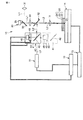
本発明の第1の実施形態に係る液晶パネルの欠陥画素修正装置を、図1を用いて説明する。図1は、修正装置10の概略的構成図である。修正装置10は、液晶パネル20の輝点欠陥21を修正する装置である。
A defective pixel correcting device for a liquid crystal panel according to a first embodiment of the present invention will be described with reference to FIG. FIG. 1 is a schematic configuration diagram of the
図1に示すように、液晶パネル20は、パネル本体22と、偏光板23と、保護フィルム24とを備えている。パネル本体22は、図示しない一対のガラス基板と、これら一対のガラス基板間に収容される液晶とを備えて構成されている。
As shown in FIG. 1, the
一方のガラス基板は、アレイ基板となっている。アレイ基板には、多数本の信号線とGate線とがマトリクス状に形成されている。信号線とGate線との交差部に、画素電極に電荷を充放電するTFT(Thin Film Transistors)が設けられている。アレイ基板上には、TFTに隣接して100〜400μm程度の大きさを有する多数の画素電極がマトリクス状に設けられている。 One glass substrate is an array substrate. A large number of signal lines and gate lines are formed in a matrix on the array substrate. TFTs (Thin Film Transistors) that charge and discharge the pixel electrodes are provided at intersections between the signal lines and the Gate lines. On the array substrate, a large number of pixel electrodes having a size of about 100 to 400 μm are provided in a matrix adjacent to the TFT.
もう一方のガラス基板は、カラーフィルタ基板となっている。カラーフィルタ基板には、着色層と保護膜と透明導電膜とが形成されている。透明導電膜は、液晶パネル20の共通電極を形成するもので、カラーフィルタ基板の液晶側表面全体を覆っている。輝点欠陥21は、パネル本体22中に形成されている。輝点欠陥21は、本発明で言う欠陥画素の一例である。
The other glass substrate is a color filter substrate. A colored layer, a protective film, and a transparent conductive film are formed on the color filter substrate. The transparent conductive film forms a common electrode of the
液晶パネル20では、TFTが誤差動する部位があったり、または、画素電極が正常に形成されない部位がある場合に、これらの不良部に対応する画素が透過光を遮断することができなくなる。このような場合、この画素は輝点欠陥として現れる。
In the
偏光板23は、パネル本体22の表面に設けられている。保護フィルム24は、偏光板23の表面に設けられている。
The polarizing
修正装置10は、レーザ出力部11と、第1のミラー12と、第1の集光レンズ13と、液晶パネル20が載置されるXYステージ14と、ステージ駆動部15と、制御部16と、観察部30と、計測機構40とを備えている。
The
レーザ出力部11は、XYステージ14に載置された液晶パネル20に向かってレーザを出力する。レーザ出力部11は、出力するレーザの強度を調整する機能を有している。
The
第1のミラー12は、レーザの光路上においてレーザ出力部11の下流に配置されており、レーザの一部を反射してその光路を変更している。第1のミラー12の透過率および反射率は、予め、求められている。
The
第1の集光レンズ13は、レーザの光路上において第1のミラー12の下流に配置されている。第1の集光レンズ13は、第1のミラー12によって反射されたレーザを集光する。
The
ステージ駆動部15は、XYステージ14を駆動する。具体的には、ステージ駆動部15は、液晶パネル20中の輝点欠陥21を、第1の集光レンズ13によって集光されたレーザによる加工点上に移動する。
The
観察部30は、光源31と、第2のミラー32と、第2の集光レンズ33と、CCDカメラ35とを備えている。
The
光源31は、液晶パネル20に向かって光L1を出力する。なお、図中、光L1は、1点鎖線で示されており、一部は省略されている。
The
第2のミラー32は、光源31の光路において光源31の下流に配置されている。光源31から出力された光L1の一部は、第2のミラー32に反射されてその光路が変更され、第2の集光レンズ33に導かれる。第2のミラー32の透過率および反射率は、予め求められている。
The
第2の集光レンズ33は、光源31の光路において第2のミラー32の下流に配置されている。第2の集光レンズ33に到達した光は、第2の集光レンズ33によって集光される。第2の集光レンズ33で集光された光L1の一部は、第1のミラー12と第1の集光レンズ13とを透過して、レーザ出力部11によって出力されたレーザによる加工点に到達する。
The
CCDカメラ35は、光源31の光路において加工点の下流に配置されている。加工点に導かれた光L1は、輝点欠陥21で反射した後、光源31から輝点欠陥21までの往路をそのまま逆向きに進み、その過程で第1,2の集光レンズ13,33及び第1、2のミラー12、32とを透過して、CCDカメラ35に到達し撮影される。観察部30は、上記構成によって、液晶パネル20上の輝点欠陥21の様子をモニタする。CCDカメラ35は、本発明で言う撮影部の一例である。
The
計測機構40は、基部41と、第3のミラー42と、偏光フィルタ43と、偏光フィルタ回転機構44と、フォトダイオード45とを備えている。第3のミラー42と、偏光フィルタ43と、偏光フィルタ回転機構44と、フォトダイオード45とは、基部41に固定されている。
The measuring
第3のミラー42は、レーザ出力部11から出力されるレーザの光路上に配置される。第3のミラー42は、輝点欠陥21で反射されたレーザの一部を反射して後述されるフォトダイオード45に導く。第3のミラー42の透過率および反射率は、予め求められている。基部41は、駆動部を有しており、移動可能である。基部41は、第3のミラー42がレーザの光路から外れる位置まで移動できる。
The
偏光フィルタ43は、輝点欠陥21で反射されたレーザの光路において第3のミラー42の下流に配置されている。偏光フィルタ43は、液晶パネル20からの反射光および外部からの光のうち、輝点欠陥21の加工部からの光と同一の偏光方向を持つ光のみを選択的に透過する。
The
具体的に説明すると、レーザ出力部11から出力されたレーザのうち、保護フィルム24の表面や偏光板23の表面で反射したレーザは、輝点欠陥21で反射されたレーザの偏光方向とは異なる。それゆえ、偏光フィルタ43の配置方向を輝点欠陥21で反射したレーザの偏光方向に合わせることによって、輝点欠陥21からの反射光を選択的に透過させることができる。
More specifically, among the lasers output from the
偏光フィルタ回転機構44は、偏光フィルタ43の配置方向を任意の方向に調整する。フォトダイオード45は、輝点欠陥21で反射されたレーザの光路において偏光フィルタ43の下流に配置されている。フォトダイオード45は、輝点欠陥21で反射されたレーザの強度を計測する。
The polarization
制御部16は、レーザ出力部11とステージ駆動部15と基部41と偏光フィルタ回転機構44の動作を制御する。また、制御部16は、レーザ出力部11から出力されたレーザの強度とフォトダイオード45によって計測されたレーザの強度とを比較し、輝点欠陥21に到達するまでに損失されるレーザの損失割合を求める。
The
つぎに、液晶パネル20の輝点欠陥21を修正する場合を一例に、修正装置10の動作を説明する。
Next, the operation of the
まず、液晶パネル20がXYステージ14上に載置される。ついで、輝点欠陥21の位置を加工点上に移動すべく、ステージ駆動部15が駆動される。さらに、第3のミラー42がレーザの光路上に配置されるように、計測機構40の基部41が駆動される。
First, the
ついで、レーザ出力部11から計測用レーザL2が照射される。なお、計測用レーザL2は、強度の弱いレーザである。具体的には、計測用レーザL2の強度は、輝点欠陥21を修正するために必要と想定される強度よりも弱い。
Subsequently, the laser L2 for measurement is irradiated from the
なお、レーザ出力部11が出力するレーザは、保護フィルム24と偏光板23とを加工することがなく、かつ、パネル本体22の各ガラス基板に形成される配線だけを切断するためにメタル系の材料に吸収される波長が用いられている。
Note that the laser output from the
計測用レーザL2の一部は、第3のミラー42を透過する。第3のミラー42を透過する計測用レーザL2の強度は、第3のミラー42の透過率に対応する。
A part of the measurement laser L2 passes through the
第3のミラー42を透過した計測用レーザL2は、第1のミラー12によってその光路が変更される。第1のミラー12によって反射される計測用レーザL2の強度は、第1のミラー12の反射率に対応する。第1のミラー12で反射された計測用レーザL2は、第1の集光レンズ13によって集光された後、液晶パネル20に到達する。
The optical path of the measurement laser L <b> 2 that has passed through the
液晶パネル20に到達した計測用レーザL2は、まず保護フィルム24に入射する。保護フィルム24の表面には、液晶パネル20の搬送過程における外的要因によって、傷がついていることがある。
The measurement laser L2 that reaches the
この傷によって保護フィルム24に到達した計測用レーザL2のうち一部は、反射する。それゆえ、保護フィルム24を通過する計測用レーザL2は、保護フィルム24に到達した計測用レーザL2のうちの一部である。なお、保護フィルム24の表面に形成される傷は、液晶パネル20を破壊するほど大きいものではなく、液晶パネル20を移動したりするなど液晶パネル20の製造過程で自然に形成されるものである。
A part of the measurement laser L2 that reaches the
保護フィルム24を透過した計測用レーザL2は、偏光板23に到達する。偏光板23に到達した計測用レーザL2は、偏光板23を透過して偏光板23の偏光方向に沿った直線偏光になる。それゆえ、偏光板23を透過する計測用レーザL2は、偏光板23に到達した計測用レーザL2のうち一部である。
The measurement laser L 2 that has passed through the
偏光板23を透過した計測用レーザL2は、輝点欠陥21に到達する。上記のように、輝点欠陥21に到達する計測用レーザL2は、第1,3のミラー12,42による影響と保護フィルム24による影響と偏光板23による影響とによって、レーザ出力部11から出力された計測用レーザL2のうち一部である。
The measurement laser L 2 that has passed through the
輝点欠陥21に到達した計測用レーザL2は、輝点欠陥21で反射される。反射された計測用レーザL2は、偏光板23を透過し、保護フィルム24に到達する。
The measurement laser L 2 that has reached the
保護フィルム24において偏光板23側の表面には傷がつきにくく、それゆえ、傷による光の散乱の影響を略無視できるので、反射後、保護フィルム24に到達する計測用レーザL2は、略そのまま保護フィルム24を透過する。
In the
保護フィルム24を透過した計測用レーザL2の一部は、第1のミラー12で再び反射される。第1のミラー12で再び反射された計測用レーザL2は、第3のミラー42に到達する。第3のミラー42に到達した計測用レーザL2の一部は、第3のミラー42で反射されて偏光フィルタ43に到達する。
A part of the measurement laser L 2 that has passed through the
偏光フィルタ43の配置方向は、偏光フィルタ回転機構44によって、予め反射された計測用レーザL2の偏光方向と同一方向に調整されている。それゆえ、偏光フィルタ43に到達した計測用レーザL2のうち、輝点欠陥21からの反射光は、略そのままフォトダイオード45に到達する。フォトダイオード45は、到達した計測用レーザL2の強度を計測する。
The arrangement direction of the
フォトダイオード45で計測された計測用レーザL2は、輝点欠陥21に到達した計測用レーザL2が第1,3のミラー12,42で反射したものである。それゆえ、第1,3の12,42での反射率に基づいて逆算することによって、輝点欠陥21に到達した計測用レーザL2の強度が求められる。
The measurement laser L2 measured by the
上記のように求められた輝点欠陥21に到達した計測用レーザL2の強度とレーザ出力部11から出力された計測用レーザL2の強度とを比較し、レーザ出力部11から出力された計測用レーザL2のうち輝点欠陥21に到達するまでに損失された計測用レーザL2の損失割合が求められる。
The intensity of the measurement laser L2 that has reached the
ついで、制御部16は、第3のミラー42が光路上から外れるように、計測機構40の基部41を移動させる。
Next, the
ついで、制御部16は、輝点欠陥21を修正するためにレーザ出力部11から出力されるべきレーザの強度を求める。具体的には、輝点欠陥21を修正するためにレーザ出力部11から照射されるべきレーザの強度は、予め計測された保護フィルム24および偏光板23による影響を無視した場合における輝点欠陥21を修正するために必要なレーザの強度に、上記の損失割合を考慮した上乗せ分が付加された強度となる。
Next, the
なお、保護フィルム24および偏光板23による影響を無視した場合における輝点欠陥21を修正するために必要なレーザの強度は、液晶パネル20に固有のものではなく、同じように製造された液晶パネルに対して共通の値となる。それゆえ、予めこの種の液晶パネルの修正用のために、保護フィルム24および偏光板23がない状態における輝点欠陥を修正するために必要なレーザの強度を求めておくことが好ましい。
Note that the intensity of the laser necessary for correcting the
ついで、制御部16は、レーザ出力部11からレーザを照射させる。このレーザによって、輝点欠陥21は修正される。
Next, the
このように構成される液晶パネルの欠陥画素修正装置10では、修正前に必要なレーザ強度が分かるため、修正の成功率が向上する。更に、一つの輝点欠陥を修正するために、計測用と修正用との計2回レーザを出力すればよいので、一つの輝点欠陥を修正するために必要なレーザの出力回数が抑えられ、輝点欠陥を修正する修正作業の効率が向上する。
In the defective
また、計測機構40の基部41が移動可能であって修正用のレーザが出力される際には第3のミラー42が光路上に位置しないので、修正用レーザは、第3のミラー42よる影響を受けることなく輝点欠陥21に到達する。それゆえ、第3のミラー42による修正用のレーザの強度ロスが無くなるので、輝点欠陥21が効率よく修正される。なお、本実施形態では、基部41が移動することによって第3のミラー42が移動されるが、これに限定されない。例えば、第3のミラー42だけが移動可能になっていてもよい。
Further, when the
また、計測機構40が偏光フィルタ回転機構44を備えていることによって、偏光フィルタ43の配置方向を、反射した計測用レーザL2の偏光方向に合わせることができる。それゆえ、反射した計測用レーザL2を精度よく計測できるようになる。
Further, since the
つぎに、本発明の第2の実施形態に係る液晶パネルの欠陥画素修正装置を、図2を用いて説明する。なお、第1の実施形態と同様な機能を有する構成は同一の符号を付して説明を省略する。本実施形態では、観察部の光源を利用して、レーザ出力部11から出力されるべき修正用レーザの出力を求める点が第1の実施形態と異なる。他の点については、第1の実施形態と同様であってよい。上記異なる点について、具体的に説明する。
Next, a defective pixel correcting device for a liquid crystal panel according to a second embodiment of the present invention will be described with reference to FIG. In addition, the structure which has the same function as 1st Embodiment attaches | subjects the same code | symbol, and abbreviate | omits description. The present embodiment is different from the first embodiment in that the output of the correction laser to be output from the
図2は、本実施形態の修正装置10を示している。図2に示すように、本実施形態では、修正装置10は、バンドパスフィルタ100を備えている。バンドパスフィルタ100は、光源31から出力される光L1の光路において第2のミラー32よりも下流であってかつCCDカメラ35の上流に配置されている。バンドパスフィルタ100は、光路の光軸に垂直に設置されている。
FIG. 2 shows the
バンドパスフィルタ100は、光源31から出力された光L1のうち、レーザ出力部11から出力される計測用レーザL2の波長またはその近傍の波長の光の一部を透過する。
The band-pass filter 100 transmits a part of the light of the wavelength of the measurement laser L2 output from the
このため、光源31から出力された光L1のうち、レーザ出力部11から出力されるレーザの波長またはその近傍の波長の光においてバンドパスフィルタ100を透過した一部がCCDカメラ35によって撮影される。光L1のうちレーザ出力部11から出力されるレーザの波長の近傍の波長の光が輝点欠陥21に到達するまでの損失割合は、光源31から出力される光L1のうちレーザ出力部11から出力されるレーザの波長と同じ波長を有する光と略同じである。
Therefore, a part of the light L1 output from the
それゆえ、光源31から出力される光L1のうちレーザ出力部11から出力されるレーザの波長またはその近傍の波長の光の損失割合を調べることによって、レーザ出力部11から出力されるレーザが輝点欠陥21に到達するまでの損失割合が求められる。本実施形態では、バンドパスフィルタ100は、レーザ出力部11から出力されるレーザと同じ例えば530nmの波長の光の一部を透過する。
Therefore, the laser output from the
光源31から出力される光L1の光路において第2のミラー32とバンドパスフィルタ100との間には、偏光フィルタ43が配置されている。偏光フィルタ43は、偏光フィルタ回転機構44によって配置方向が任意の方向に調整される。
A
つぎに、本実施形態の修正装置10の動作を説明する。まず、光源31から光L1が出力される。光L1に含まれる例えば530nmの波長の光の強度は、予め求められている。光L1のうち一部は、第2のミラー32によって反射される。光L1のうち530nmの波長の光の一部は、第2のミラー32で反射されるとともに第2のミラー32を透過する。
Next, the operation of the
第2のミラー32で反射された光L1の一部は、第1のミラー12を透過する。第1のミラー12を透過した光L1のうち一部は、第1の実施形態で説明されたように、保護フィルム24と偏光板23とを透過した後、輝点欠陥21に到達する。
A part of the light L 1 reflected by the
輝点欠陥21に到達した光L1は、輝点欠陥21にて反射された後、偏光板23と保護フィルム24と第1,2のミラー12,32とを透過してバンドパスフィルタ100に到達する。バンドパスフィルタ100に到達した光L1のうち530nmの波長の光の一部のみがバンドパスフィルタ100を透過する。
The light L 1 that has reached the
バンドパスフィルタ100を透過した530nmの波長の光は、偏光フィルタ43に到達する。偏光フィルタ43の配置方向は、偏光フィルタ回転機構44によって、予め反射された光L1の偏光方向と同一方向に調整されている。偏光フィルタ43を透過した光L1は、CCDカメラ35に到達し、撮影される。CCDカメラ35は、バンドパスフィルタ100を透過した530nmの光の強度を計測する。
The light having a wavelength of 530 nm transmitted through the bandpass filter 100 reaches the
上記のように、CCDカメラ35によって計測された530nmの光の強度は、輝点欠陥21に到達した530nmの波長の光のうち第1のミラー12と第2のミラー32で反射された分とバンドパスフィルタ100を透過しなかった分とを差し引いた分の強度である。
As described above, the intensity of the light of 530 nm measured by the
それゆえ、CCDカメラ35で計測された530nnの波長の光の強度に、第1のミラー12と第2のミラー32で反射した分とバンドパスフィルタ100を透過しなかった分を考慮した分を追加した強度が、輝点欠陥21に到達した波長の光の強度になる。
Therefore, the amount of light having a wavelength of 530 nn measured by the
制御部16では、上記のように得られた輝点欠陥21に到達した530nmの波長の光の強度と光源31から出力された光L1中の530nmの光の強度とを比較することによって、530nmの波長の光の損失割合を求める。530nmの光の損失割合は、レーザ出力部11から出力されるレーザの損失割合と略同じである。
The
制御部16は、得られた損失割合に基づいて、輝点欠陥21を修正するため必要なレーザの強度を求める。
The
本実施形態の修正装置10では、別途に計測機構40を用意することなく、既存の観察部30を利用してレーザの損失割合を求めている。それゆえ、修正装置10の構造を複雑にすることがなく、簡素な構造にすることができる。
In the
10…液晶パネルの欠陥画素修正装置、11…レーザ出力部、20…液晶パネル、21…輝点欠陥(欠陥画素)、30…観察部、31…光源、35…CCDカメラ(撮影部)、40…計測機構、43…偏光フィルタ、100…バンドパスフィルタ、L1…光、L2…計測用レーザ(レーザ)。
DESCRIPTION OF
Claims (4)
レーザを出力するとともに、前記レーザの強度を調整する調整機能を有するレーザ出力部と、
前記欠陥画素から反射された前記レーザの強度を計測する計測機構と、
を具備することを特徴とする液晶パネルの欠陥画素修正装置。 A defective pixel correction device for a liquid crystal panel that corrects the defective pixel by irradiating a defective pixel on the liquid crystal panel with a laser,
A laser output unit that outputs a laser and has an adjustment function of adjusting the intensity of the laser;
A measurement mechanism for measuring the intensity of the laser reflected from the defective pixel;
An apparatus for correcting defective pixels of a liquid crystal panel, comprising:
前記欠陥画素から反射されたレーザを偏光する偏光フィルタと、
前記偏光フィルタを任意の配置方向に固定するように前記偏光フィルタを回転し保持する回転機構と、
を備えることを特徴とする請求項1に記載の液晶パネルの欠陥画素修正装置。 The measuring mechanism is
A polarizing filter for polarizing the laser reflected from the defective pixel;
A rotating mechanism for rotating and holding the polarizing filter so as to fix the polarizing filter in an arbitrary arrangement direction;
The defective pixel correction device for a liquid crystal panel according to claim 1, comprising:
レーザを出力するとともに、前記レーザの強度を調整する調整機能を有するレーザ出力部と、
前記欠陥画素に向かって観察用の光を出力する光源と、前記欠陥画素で反射される光のうち特定の波長の光の一部を透過するバンドパスフィルタと、前記欠陥画素で反射され前記バンドパスフィルタを透過した光を撮影する撮影部とを具備する観察部と、
を具備することを特徴とする液晶パネルの欠陥画素修正装置。 A defective pixel correction device for a liquid crystal panel that corrects the defective pixel by irradiating a defective pixel on the liquid crystal panel with a laser,
A laser output unit that outputs a laser and has an adjustment function of adjusting the intensity of the laser;
A light source that outputs observation light toward the defective pixel, a band-pass filter that transmits a part of light having a specific wavelength among light reflected by the defective pixel, and the band reflected by the defective pixel An observation unit comprising an imaging unit for imaging light transmitted through the pass filter;
An apparatus for correcting defective pixels of a liquid crystal panel, comprising:
Priority Applications (5)
| Application Number | Priority Date | Filing Date | Title |
|---|---|---|---|
| JP2006027394A JP2007206550A (en) | 2006-02-03 | 2006-02-03 | Defective pixel correcting device for liquid crystal panel |
| TW095132582A TW200730925A (en) | 2006-02-03 | 2006-09-04 | Defective pixel compensation device for liquid-crystal display panel |
| US11/534,006 US7564543B2 (en) | 2006-02-03 | 2006-09-21 | Defective pixel correction apparatus for liquid crystal panel |
| CNB2006101429861A CN100541271C (en) | 2006-02-03 | 2006-10-26 | The defective pixel correction apparatus of liquid crystal panel |
| KR1020060107513A KR100837456B1 (en) | 2006-02-03 | 2006-11-02 | Apparatus for correcting a defect pixel in a liquid crystal panel |
Applications Claiming Priority (1)
| Application Number | Priority Date | Filing Date | Title |
|---|---|---|---|
| JP2006027394A JP2007206550A (en) | 2006-02-03 | 2006-02-03 | Defective pixel correcting device for liquid crystal panel |
Publications (2)
| Publication Number | Publication Date |
|---|---|
| JP2007206550A true JP2007206550A (en) | 2007-08-16 |
| JP2007206550A5 JP2007206550A5 (en) | 2009-03-19 |
Family
ID=38333726
Family Applications (1)
| Application Number | Title | Priority Date | Filing Date |
|---|---|---|---|
| JP2006027394A Pending JP2007206550A (en) | 2006-02-03 | 2006-02-03 | Defective pixel correcting device for liquid crystal panel |
Country Status (5)
| Country | Link |
|---|---|
| US (1) | US7564543B2 (en) |
| JP (1) | JP2007206550A (en) |
| KR (1) | KR100837456B1 (en) |
| CN (1) | CN100541271C (en) |
| TW (1) | TW200730925A (en) |
Cited By (1)
| Publication number | Priority date | Publication date | Assignee | Title |
|---|---|---|---|---|
| CN103372721A (en) * | 2012-04-27 | 2013-10-30 | 株式会社迪思科 | Laser processor and laser processing method |
Families Citing this family (8)
| Publication number | Priority date | Publication date | Assignee | Title |
|---|---|---|---|---|
| CN101957531B (en) * | 2009-07-21 | 2013-04-03 | 北京京东方光电科技有限公司 | Array substrate maintenance equipment and method |
| JP5552829B2 (en) * | 2010-02-15 | 2014-07-16 | マツダ株式会社 | Automobile undercarriage |
| US9304090B2 (en) * | 2013-03-11 | 2016-04-05 | Electro Scientific Industries, Inc. | Systems and methods for providing polarization compensated multi-spectral laser repair of liquid crystal display panels |
| CN103676234B (en) * | 2013-11-29 | 2016-06-01 | 合肥京东方光电科技有限公司 | A kind of detection device, array substrate detection system and method thereof |
| CN105866991B (en) * | 2016-06-21 | 2019-02-26 | 京东方科技集团股份有限公司 | Display panel method for maintaining, device, equipment and system |
| CN105954904B (en) * | 2016-07-20 | 2019-03-15 | 京东方科技集团股份有限公司 | The method for maintaining and device of display module |
| JP7105639B2 (en) * | 2018-07-05 | 2022-07-25 | 浜松ホトニクス株式会社 | Laser processing equipment |
| KR102379203B1 (en) * | 2020-08-19 | 2022-03-28 | 한국디지털포렌식기술표준원 주식회사 | Digital forensics for data recovery of portable electronic devices with alignment means using light source and filter |
Citations (14)
| Publication number | Priority date | Publication date | Assignee | Title |
|---|---|---|---|---|
| JPH0337492A (en) * | 1989-07-04 | 1991-02-18 | Fujitsu Ltd | Gas pipe |
| JPH06242410A (en) * | 1993-02-17 | 1994-09-02 | Nec Corp | Lcd display body inspecting device |
| JPH06252485A (en) * | 1992-12-28 | 1994-09-09 | Mitsubishi Electric Corp | Laser processing machine |
| JPH071173A (en) * | 1993-06-18 | 1995-01-06 | Hoya Corp | Laser beam machining device with observation function |
| JPH07124764A (en) * | 1993-10-28 | 1995-05-16 | Nec Corp | Laser beam machining device |
| JPH1190659A (en) * | 1997-09-22 | 1999-04-06 | Nikon Corp | Laser repairing device |
| JPH11132750A (en) * | 1997-10-30 | 1999-05-21 | Matsushita Electric Ind Co Ltd | Point defect detecting device and method therefor |
| JP2002066771A (en) * | 2000-08-16 | 2002-03-05 | Toshiba Corp | Laser system |
| JP2002214159A (en) * | 2001-01-12 | 2002-07-31 | Sony Corp | Substrate inspecting device, substrate inspecting method, and manufacturing method for liquid crystal display device |
| JP2003029228A (en) * | 2001-07-11 | 2003-01-29 | Hamamatsu Photonics Kk | Method for correcting defect, and liquid crystal display |
| JP2003029226A (en) * | 2001-07-11 | 2003-01-29 | Hamamatsu Photonics Kk | Method for correcting luminescent spot defect |
| JP2003029227A (en) * | 2001-07-11 | 2003-01-29 | Hamamatsu Photonics Kk | Method for correcting luminescent spot defect and liquid crystal indicator |
| JP2004170109A (en) * | 2002-11-18 | 2004-06-17 | Matsushita Electric Ind Co Ltd | Apparatus and method for inspecting irregular color |
| JP2005033007A (en) * | 2003-07-14 | 2005-02-03 | Sumitomo Heavy Ind Ltd | Method and device for correcting energy variation of laser beam |
Family Cites Families (15)
| Publication number | Priority date | Publication date | Assignee | Title |
|---|---|---|---|---|
| US5280374A (en) * | 1991-03-01 | 1994-01-18 | Sharp Kabushiki Kaisha | Liquid crystal display device and method of compensating for a defect |
| JP2799080B2 (en) | 1991-03-18 | 1998-09-17 | 株式会社日立製作所 | Laser processing method and apparatus, transmission type liquid crystal element, wiring pattern defect correcting method and apparatus |
| JP3063688B2 (en) * | 1997-07-30 | 2000-07-12 | 日本電気株式会社 | Laser processing apparatus, control method therefor, and recording medium storing control program therefor |
| JP2001133803A (en) | 1999-11-01 | 2001-05-18 | Toshiba Corp | Method of producing liquid crystal display device, liquid crystal display device and laser repair device |
| JP3460678B2 (en) | 2000-06-02 | 2003-10-27 | 松下電器産業株式会社 | Laser processing method and processing apparatus |
| JP2001351876A (en) * | 2000-06-05 | 2001-12-21 | Sumitomo Heavy Ind Ltd | Apparatus and method for laser processing |
| EP1215525A3 (en) * | 2000-12-14 | 2005-03-16 | Mitsubishi Denki Kabushiki Kaisha | Method and apparatus for detecting gap of liquid-crystal panel and apparatus therefor |
| JP3673742B2 (en) | 2001-09-27 | 2005-07-20 | レーザーフロントテクノロジーズ株式会社 | Bright spot defect correcting method and apparatus for liquid crystal display device |
| JP3742353B2 (en) * | 2002-03-07 | 2006-02-01 | 株式会社東芝 | Defective pixel correction method for liquid crystal display device and defective pixel correction device for liquid crystal display device |
| KR100457565B1 (en) | 2002-07-29 | 2004-11-18 | 엘지전자 주식회사 | laser repair device and method |
| JP2004160520A (en) * | 2002-11-15 | 2004-06-10 | Toshiba Corp | Method and device for correcting defective pixel of liquid crystal display, and manufacturing method of liquid crystal display |
| JP2005275135A (en) * | 2004-03-25 | 2005-10-06 | Toshiba Corp | Method and apparatus for correcting defective pixel of liquid crystal display |
| JP2006091671A (en) | 2004-09-27 | 2006-04-06 | Toshiba Corp | Defect pixel correction method and detect pixel correcting device for liquid crystal display |
| JP2006091672A (en) | 2004-09-27 | 2006-04-06 | Toshiba Corp | Defect pixel correcting method for liquid crystal display, and liquid crystal display |
| JP4723915B2 (en) * | 2005-06-03 | 2011-07-13 | 株式会社東芝 | Method and apparatus for repairing liquid crystal panel |
-
2006
- 2006-02-03 JP JP2006027394A patent/JP2007206550A/en active Pending
- 2006-09-04 TW TW095132582A patent/TW200730925A/en not_active IP Right Cessation
- 2006-09-21 US US11/534,006 patent/US7564543B2/en not_active Expired - Fee Related
- 2006-10-26 CN CNB2006101429861A patent/CN100541271C/en not_active Expired - Fee Related
- 2006-11-02 KR KR1020060107513A patent/KR100837456B1/en not_active IP Right Cessation
Patent Citations (14)
| Publication number | Priority date | Publication date | Assignee | Title |
|---|---|---|---|---|
| JPH0337492A (en) * | 1989-07-04 | 1991-02-18 | Fujitsu Ltd | Gas pipe |
| JPH06252485A (en) * | 1992-12-28 | 1994-09-09 | Mitsubishi Electric Corp | Laser processing machine |
| JPH06242410A (en) * | 1993-02-17 | 1994-09-02 | Nec Corp | Lcd display body inspecting device |
| JPH071173A (en) * | 1993-06-18 | 1995-01-06 | Hoya Corp | Laser beam machining device with observation function |
| JPH07124764A (en) * | 1993-10-28 | 1995-05-16 | Nec Corp | Laser beam machining device |
| JPH1190659A (en) * | 1997-09-22 | 1999-04-06 | Nikon Corp | Laser repairing device |
| JPH11132750A (en) * | 1997-10-30 | 1999-05-21 | Matsushita Electric Ind Co Ltd | Point defect detecting device and method therefor |
| JP2002066771A (en) * | 2000-08-16 | 2002-03-05 | Toshiba Corp | Laser system |
| JP2002214159A (en) * | 2001-01-12 | 2002-07-31 | Sony Corp | Substrate inspecting device, substrate inspecting method, and manufacturing method for liquid crystal display device |
| JP2003029228A (en) * | 2001-07-11 | 2003-01-29 | Hamamatsu Photonics Kk | Method for correcting defect, and liquid crystal display |
| JP2003029226A (en) * | 2001-07-11 | 2003-01-29 | Hamamatsu Photonics Kk | Method for correcting luminescent spot defect |
| JP2003029227A (en) * | 2001-07-11 | 2003-01-29 | Hamamatsu Photonics Kk | Method for correcting luminescent spot defect and liquid crystal indicator |
| JP2004170109A (en) * | 2002-11-18 | 2004-06-17 | Matsushita Electric Ind Co Ltd | Apparatus and method for inspecting irregular color |
| JP2005033007A (en) * | 2003-07-14 | 2005-02-03 | Sumitomo Heavy Ind Ltd | Method and device for correcting energy variation of laser beam |
Cited By (2)
| Publication number | Priority date | Publication date | Assignee | Title |
|---|---|---|---|---|
| CN103372721A (en) * | 2012-04-27 | 2013-10-30 | 株式会社迪思科 | Laser processor and laser processing method |
| TWI584899B (en) * | 2012-04-27 | 2017-06-01 | Disco Corp | Laser processing device and laser processing method (2) |
Also Published As
| Publication number | Publication date |
|---|---|
| US20070182954A1 (en) | 2007-08-09 |
| TWI349801B (en) | 2011-10-01 |
| CN100541271C (en) | 2009-09-16 |
| KR20070079901A (en) | 2007-08-08 |
| CN101013206A (en) | 2007-08-08 |
| TW200730925A (en) | 2007-08-16 |
| KR100837456B1 (en) | 2008-06-12 |
| US7564543B2 (en) | 2009-07-21 |
Similar Documents
| Publication | Publication Date | Title |
|---|---|---|
| KR100837456B1 (en) | Apparatus for correcting a defect pixel in a liquid crystal panel | |
| US9821408B2 (en) | Laser machining method and laser machining device | |
| US9304090B2 (en) | Systems and methods for providing polarization compensated multi-spectral laser repair of liquid crystal display panels | |
| JP2007241274A5 (en) | ||
| TWI640804B (en) | Device for manufacturing optical member bonded body | |
| US8928853B2 (en) | Method and system for repairing flat panel display | |
| TW201738026A (en) | Laser beam irradiating device | |
| US20160299365A1 (en) | Laser Repairing Apparatus | |
| JP2006300811A (en) | Method of measuring film thickness of thin film, method of forming polycrystal semiconductor thin film, manufacturing method for semiconductor device, manufacturing apparatus for the same, and manufacture method for image display | |
| WO2014119779A1 (en) | Laser repair device | |
| TWI553981B (en) | Laser processing apparatus and method | |
| JP6327735B2 (en) | Bright spot defect removal method and apparatus for liquid crystal display panel | |
| JP2005009919A (en) | Inspection device and inspecting method for polarization plate with protective film | |
| KR20100058012A (en) | Optical system for detecting defect | |
| JP2021534456A (en) | Laser repair and inspection method for display device panel and suitable repair and inspection device | |
| JP5230240B2 (en) | Laser processing equipment | |
| JP2007203334A (en) | Substrate, electrooptical device and electronic equipment, manufacturing method of substrate, manufacturing method of electrooptical device | |
| JP2006329715A (en) | Deterioration tester and deterioration testing method | |
| KR20160089277A (en) | Method for testing laser beam | |
| JP2004335717A (en) | Laser repairing apparatus | |
| JP2006326629A (en) | Laser beam machining apparatus and its machining method | |
| JP2008023579A (en) | Method for severing substrate, method for manufacturing electro-optical apparatus and laser scribing device | |
| KR100685145B1 (en) | Apparatus for repairing colorfilter | |
| KR20090114214A (en) | Method and apparatus for repairing a defect of liquid crystal display panel | |
| JP7386511B2 (en) | Laser processing equipment |
Legal Events
| Date | Code | Title | Description |
|---|---|---|---|
| A521 | Written amendment |
Free format text: JAPANESE INTERMEDIATE CODE: A523 Effective date: 20090203 |
|
| A621 | Written request for application examination |
Free format text: JAPANESE INTERMEDIATE CODE: A621 Effective date: 20090203 |
|
| A977 | Report on retrieval |
Free format text: JAPANESE INTERMEDIATE CODE: A971007 Effective date: 20110608 |
|
| A131 | Notification of reasons for refusal |
Free format text: JAPANESE INTERMEDIATE CODE: A131 Effective date: 20110705 |
|
| A02 | Decision of refusal |
Free format text: JAPANESE INTERMEDIATE CODE: A02 Effective date: 20111108 |