JP2007156419A - Data driving integrated circuit device and liquid crystal display device including the same - Google Patents
Data driving integrated circuit device and liquid crystal display device including the same Download PDFInfo
- Publication number
- JP2007156419A JP2007156419A JP2006221659A JP2006221659A JP2007156419A JP 2007156419 A JP2007156419 A JP 2007156419A JP 2006221659 A JP2006221659 A JP 2006221659A JP 2006221659 A JP2006221659 A JP 2006221659A JP 2007156419 A JP2007156419 A JP 2007156419A
- Authority
- JP
- Japan
- Prior art keywords
- data
- liquid crystal
- gamma
- crystal display
- differential
- Prior art date
- Legal status (The legal status is an assumption and is not a legal conclusion. Google has not performed a legal analysis and makes no representation as to the accuracy of the status listed.)
- Pending
Links
Images


Classifications
-
- G—PHYSICS
- G09—EDUCATION; CRYPTOGRAPHY; DISPLAY; ADVERTISING; SEALS
- G09G—ARRANGEMENTS OR CIRCUITS FOR CONTROL OF INDICATING DEVICES USING STATIC MEANS TO PRESENT VARIABLE INFORMATION
- G09G3/00—Control arrangements or circuits, of interest only in connection with visual indicators other than cathode-ray tubes
- G09G3/20—Control arrangements or circuits, of interest only in connection with visual indicators other than cathode-ray tubes for presentation of an assembly of a number of characters, e.g. a page, by composing the assembly by combination of individual elements arranged in a matrix no fixed position being assigned to or needed to be assigned to the individual characters or partial characters
- G09G3/34—Control arrangements or circuits, of interest only in connection with visual indicators other than cathode-ray tubes for presentation of an assembly of a number of characters, e.g. a page, by composing the assembly by combination of individual elements arranged in a matrix no fixed position being assigned to or needed to be assigned to the individual characters or partial characters by control of light from an independent source
- G09G3/36—Control arrangements or circuits, of interest only in connection with visual indicators other than cathode-ray tubes for presentation of an assembly of a number of characters, e.g. a page, by composing the assembly by combination of individual elements arranged in a matrix no fixed position being assigned to or needed to be assigned to the individual characters or partial characters by control of light from an independent source using liquid crystals
- G09G3/3611—Control of matrices with row and column drivers
- G09G3/3685—Details of drivers for data electrodes
- G09G3/3688—Details of drivers for data electrodes suitable for active matrices only
-
- G—PHYSICS
- G02—OPTICS
- G02F—OPTICAL DEVICES OR ARRANGEMENTS FOR THE CONTROL OF LIGHT BY MODIFICATION OF THE OPTICAL PROPERTIES OF THE MEDIA OF THE ELEMENTS INVOLVED THEREIN; NON-LINEAR OPTICS; FREQUENCY-CHANGING OF LIGHT; OPTICAL LOGIC ELEMENTS; OPTICAL ANALOGUE/DIGITAL CONVERTERS
- G02F1/00—Devices or arrangements for the control of the intensity, colour, phase, polarisation or direction of light arriving from an independent light source, e.g. switching, gating or modulating; Non-linear optics
- G02F1/01—Devices or arrangements for the control of the intensity, colour, phase, polarisation or direction of light arriving from an independent light source, e.g. switching, gating or modulating; Non-linear optics for the control of the intensity, phase, polarisation or colour
- G02F1/13—Devices or arrangements for the control of the intensity, colour, phase, polarisation or direction of light arriving from an independent light source, e.g. switching, gating or modulating; Non-linear optics for the control of the intensity, phase, polarisation or colour based on liquid crystals, e.g. single liquid crystal display cells
- G02F1/133—Constructional arrangements; Operation of liquid crystal cells; Circuit arrangements
-
- G—PHYSICS
- G09—EDUCATION; CRYPTOGRAPHY; DISPLAY; ADVERTISING; SEALS
- G09G—ARRANGEMENTS OR CIRCUITS FOR CONTROL OF INDICATING DEVICES USING STATIC MEANS TO PRESENT VARIABLE INFORMATION
- G09G3/00—Control arrangements or circuits, of interest only in connection with visual indicators other than cathode-ray tubes
- G09G3/20—Control arrangements or circuits, of interest only in connection with visual indicators other than cathode-ray tubes for presentation of an assembly of a number of characters, e.g. a page, by composing the assembly by combination of individual elements arranged in a matrix no fixed position being assigned to or needed to be assigned to the individual characters or partial characters
- G09G3/34—Control arrangements or circuits, of interest only in connection with visual indicators other than cathode-ray tubes for presentation of an assembly of a number of characters, e.g. a page, by composing the assembly by combination of individual elements arranged in a matrix no fixed position being assigned to or needed to be assigned to the individual characters or partial characters by control of light from an independent source
- G09G3/36—Control arrangements or circuits, of interest only in connection with visual indicators other than cathode-ray tubes for presentation of an assembly of a number of characters, e.g. a page, by composing the assembly by combination of individual elements arranged in a matrix no fixed position being assigned to or needed to be assigned to the individual characters or partial characters by control of light from an independent source using liquid crystals
- G09G3/3611—Control of matrices with row and column drivers
- G09G3/3696—Generation of voltages supplied to electrode drivers
-
- G—PHYSICS
- G09—EDUCATION; CRYPTOGRAPHY; DISPLAY; ADVERTISING; SEALS
- G09G—ARRANGEMENTS OR CIRCUITS FOR CONTROL OF INDICATING DEVICES USING STATIC MEANS TO PRESENT VARIABLE INFORMATION
- G09G2300/00—Aspects of the constitution of display devices
- G09G2300/04—Structural and physical details of display devices
- G09G2300/0421—Structural details of the set of electrodes
- G09G2300/0426—Layout of electrodes and connections
-
- G—PHYSICS
- G09—EDUCATION; CRYPTOGRAPHY; DISPLAY; ADVERTISING; SEALS
- G09G—ARRANGEMENTS OR CIRCUITS FOR CONTROL OF INDICATING DEVICES USING STATIC MEANS TO PRESENT VARIABLE INFORMATION
- G09G2310/00—Command of the display device
- G09G2310/02—Addressing, scanning or driving the display screen or processing steps related thereto
- G09G2310/0264—Details of driving circuits
- G09G2310/027—Details of drivers for data electrodes, the drivers handling digital grey scale data, e.g. use of D/A converters
-
- G—PHYSICS
- G09—EDUCATION; CRYPTOGRAPHY; DISPLAY; ADVERTISING; SEALS
- G09G—ARRANGEMENTS OR CIRCUITS FOR CONTROL OF INDICATING DEVICES USING STATIC MEANS TO PRESENT VARIABLE INFORMATION
- G09G3/00—Control arrangements or circuits, of interest only in connection with visual indicators other than cathode-ray tubes
- G09G3/20—Control arrangements or circuits, of interest only in connection with visual indicators other than cathode-ray tubes for presentation of an assembly of a number of characters, e.g. a page, by composing the assembly by combination of individual elements arranged in a matrix no fixed position being assigned to or needed to be assigned to the individual characters or partial characters
- G09G3/34—Control arrangements or circuits, of interest only in connection with visual indicators other than cathode-ray tubes for presentation of an assembly of a number of characters, e.g. a page, by composing the assembly by combination of individual elements arranged in a matrix no fixed position being assigned to or needed to be assigned to the individual characters or partial characters by control of light from an independent source
- G09G3/36—Control arrangements or circuits, of interest only in connection with visual indicators other than cathode-ray tubes for presentation of an assembly of a number of characters, e.g. a page, by composing the assembly by combination of individual elements arranged in a matrix no fixed position being assigned to or needed to be assigned to the individual characters or partial characters by control of light from an independent source using liquid crystals
- G09G3/3611—Control of matrices with row and column drivers
- G09G3/3614—Control of polarity reversal in general
Abstract
Description
本発明は、データ駆動集積回路装置とこれを含む液晶表示装置に係り、さらに詳細には、製造費用を減らすことができるデータ駆動集積回路装置とこれを含む液晶表示装置に関する。 The present invention relates to a data driven integrated circuit device and a liquid crystal display device including the same, and more particularly to a data driven integrated circuit device capable of reducing manufacturing costs and a liquid crystal display device including the same.
コンピュータのモニターやTV等に使われる表示装置(display device)には、自ら発光する陰極線管(cathode―ray tube:CRT)、電界発光素子(field emission device:FED)等と、自ら発光することができなくて光源を必要とする液晶表示装置(liquid crystal display:LCD)等がある。 A display device used for a computer monitor, a TV, or the like may emit light with a cathode-ray tube (CRT), a field emission device (FED), or the like that emits light by itself. There is a liquid crystal display (LCD) that cannot be used and requires a light source.
一般的に、液晶表示装置は、結晶(Crystal)と液体(Liquid)の中間的な物性を有する液晶(Liquid Crystal)の電気光学的特性を利用して画像、文字、動映像を表示する表示装置である。 2. Description of the Related Art Generally, a liquid crystal display device displays an image, a character, and a moving image using electro-optical characteristics of a liquid crystal (Liquid Crystal) having intermediate properties between a crystal and a liquid (Liquid). It is.
従来の液晶表示装置は液晶パネル、ゲート駆動部、データ駆動部、駆動電圧生成部、タイミング制御部、及び階調電圧発生部を含み、液晶パネルにデータ駆動部及びゲート駆動部から信号が印加される。 A conventional liquid crystal display device includes a liquid crystal panel, a gate driving unit, a data driving unit, a driving voltage generating unit, a timing control unit, and a gradation voltage generating unit, and signals are applied to the liquid crystal panel from the data driving unit and the gate driving unit. The
ここで、階調電圧発生部は、データ駆動部に入る階調電圧を生成する。また、上下画素間の充電量の差を防止するために、充電低下が発生するラインに対して本来階調データによって印加されなければならない階調電圧の補償を遂行し、データ駆動部は充電低下が発生したラインに補償した階調電圧を供給する。 Here, the gradation voltage generator generates a gradation voltage that enters the data driver. In addition, in order to prevent a difference in charge amount between the upper and lower pixels, compensation is performed for the gradation voltage that must be applied by the gradation data to the line where the decrease in charge occurs, and the data driver decreases the charge. The compensated gradation voltage is supplied to the line where the occurrence of the error occurs.
従来の液晶表示装置の階調電圧発生部は、正の階調電圧と負の階調電圧とを生成するために正の階調電圧生成部と負の階調電圧生成部とを含み、正の階調電圧生成部及び負の階調電圧生成部に電圧を増幅させて提供する電圧増幅部を含んでいる。 A grayscale voltage generator of a conventional liquid crystal display device includes a positive grayscale voltage generator and a negative grayscale voltage generator to generate a positive grayscale voltage and a negative grayscale voltage. And a voltage amplifying unit for amplifying the voltage and providing the gray level voltage generating unit and the negative gradation voltage generating unit.
しかし、正の階調電圧生成部及び負の階調電圧生成部は、直列に連結された複数の抵抗を有していて、抵抗偏差によって階調電圧に変動が発生し得る。さらに、電圧増幅部は、OPアンプ(op―amp)で構成されているために、印刷回路基板を製作するとき、印刷回路基板の大きさが大きくなりうる。
本発明が解決しようとする技術的課題は、印刷回路基板の大きさを小さくすることができるデータ駆動集積回路装置を提供することにある。 The technical problem to be solved by the present invention is to provide a data driven integrated circuit device capable of reducing the size of a printed circuit board.
本発明が解決しようとする他の技術的課題は、製造費用を減らすことができるデータ駆動集積回路装置を含む液晶表示装置を提供することにある。 Another technical problem to be solved by the present invention is to provide a liquid crystal display device including a data driven integrated circuit device that can reduce manufacturing costs.
前記技術的課題を達成するための本発明のデータ駆動集積回路装置は、タイミング制御部から伝えられる差動ガンマデータを入力に受けてデコーディングして出力するガンマデコーディング部、前記デコーディングされた差動ガンマデータをアナログ電圧値に変換するデジタル/アナログ変換部、及び前記アナログ電圧値を増幅して出力するバッファー部を含む。 In order to achieve the above technical problem, the data driving integrated circuit device of the present invention includes a gamma decoding unit that receives differential gamma data transmitted from a timing control unit as an input, decodes the output, and outputs the decoded gamma data. A digital / analog conversion unit that converts the differential gamma data into an analog voltage value, and a buffer unit that amplifies and outputs the analog voltage value.
また、本発明のデータ駆動集積回路装置を含む液晶表示装置は、複数の薄膜トランジスタと、それぞれの前記薄膜トランジスタのゲート電極に連結される複数のゲート線、およびそれぞれの前記薄膜トランジスタのソース電極に連結される複数のデータ線を含む液晶パネルと、ゲート駆動部及びデータ駆動集積回路装置を駆動するための信号を生成して、前記データ駆動集積回路装置に差動ガンマデータを提供するタイミング制御部と、前記タイミング制御部から伝えられる差動ガンマデータをアナログ電圧値に変換して前記液晶パネルのデータ線に印加するデータ駆動集積回路装置と、を含む。 The liquid crystal display device including the data driving integrated circuit device of the present invention is connected to a plurality of thin film transistors, a plurality of gate lines connected to the gate electrodes of the thin film transistors, and a source electrode of the thin film transistors. A liquid crystal panel including a plurality of data lines, a timing controller for generating a signal for driving the gate driver and the data driving integrated circuit device, and providing differential gamma data to the data driving integrated circuit device; A data driving integrated circuit device that converts differential gamma data transmitted from the timing control unit into an analog voltage value and applies the analog voltage value to the data line of the liquid crystal panel.
その他実施形態の具体的な事項は詳細な説明及び図面に含まれている。 Specific matters of the other embodiments are included in the detailed description and the drawings.
上述したように、本発明の一実施形態によるデータ駆動集積回路装置とこれを含む液晶表示装置及び印刷回路基板が実装された液晶表示装置は、メモリー部の所定領域に差動ガンマデータを保存して、これをそれぞれのデータ駆動集積回路装置に伝送することによって別途の階調電圧生成部がなくても液晶表示装置の駆動が可能であり、これにより液晶表示装置の製造費用を減らすことができる。 As described above, a data driving integrated circuit device according to an embodiment of the present invention, a liquid crystal display device including the data driving integrated circuit device, and a liquid crystal display device mounted with a printed circuit board store differential gamma data in a predetermined area of a memory unit. By transmitting this to each data driving integrated circuit device, the liquid crystal display device can be driven without a separate gray voltage generator, thereby reducing the manufacturing cost of the liquid crystal display device. .
また、データ駆動集積回路装置を具現するとき、抵抗段及びOPアンプを使わずに、デコーダを追加してデータ駆動集積回路装置を構成することによって回路構成が容易にでき、また、抵抗偏差によるガンマ電圧の変動を防止することができる。さらに、印刷回路基板を製作するとき、印刷回路基板の大きさを小さくすることができる。 Further, when implementing a data driving integrated circuit device, the circuit configuration can be facilitated by configuring the data driving integrated circuit device by adding a decoder without using a resistor stage and an OP amplifier. Voltage fluctuations can be prevented. Furthermore, when the printed circuit board is manufactured, the size of the printed circuit board can be reduced.
明細書全体にかけて同一参照符号は同一構成要素を指称する。 Like reference numerals refer to like elements throughout the specification.
以下、添付した図面を参照して本発明の実施形態による液晶表示装置に関して詳細に説明する。 Hereinafter, a liquid crystal display according to an exemplary embodiment of the present invention will be described in detail with reference to the accompanying drawings.
図1は、本発明の一実施形態による液晶表示装置のブロック図である。 FIG. 1 is a block diagram of a liquid crystal display device according to an embodiment of the present invention.
図1に示したように、本発明の一実施形態による液晶表示装置は液晶パネル100、駆動電圧生成部200、ゲート駆動部300、データ駆動部400、およびタイミング制御部500を含む。
As shown in FIG. 1, the liquid crystal display according to an embodiment of the present invention includes a
液晶パネル100は、等価回路としてみると、複数の表示信号線G1―Gn,D1―Dmに連結し、マトリックス(matrix)状で配列された複数の単位画素(pixel)を含む。
When viewed as an equivalent circuit, the
ここで、表示信号線G1―Gn,D1―Dmはゲート信号を伝達する複数のゲート線G1―Gnとデータ信号を伝達するデータ線D1―Dmとを含む。ゲート線G1―Gnは行方向にのびていてお互いにほとんど平行し、データ線D1―Dmは列方向にのびていてお互いにほとんど平行する。 Here, the display signal lines G1-Gn and D1-Dm include a plurality of gate lines G1-Gn for transmitting gate signals and data lines D1-Dm for transmitting data signals. The gate lines G1 to Gn extend in the row direction and are almost parallel to each other, and the data lines D1 to Dm extend in the column direction and are almost parallel to each other.
各単位画素は、表示信号線G1―Gn,D1―Dmに連結されたスイッチング素子M、スイッチング素子Mに連結した液晶キャパシタ(liquid crystal capacitor)Clc、及び維持キャパシタ(storage capacitor)Cstを含む。維持キャパシタCstは必要によって省略することができる。 Each unit pixel includes a switching element M connected to display signal lines G1-Gn and D1-Dm, a liquid crystal capacitor Clc connected to the switching element M, and a storage capacitor Cst. The storage capacitor Cst can be omitted if necessary.
スイッチング素子Mは、TFT基板(図示せず)に具備されており、三端子素子でその制御端子及び入力端子はそれぞれゲート線G1―Gn及びデータ線D1―Dmに連結されており、出力端子は液晶キャパシタClc及び維持キャパシタCstに連結されている。 The switching element M is provided on a TFT substrate (not shown), and its control terminal and input terminal are connected to the gate line G1-Gn and the data line D1-Dm, respectively, and the output terminal is a three-terminal element. The liquid crystal capacitor Clc and the storage capacitor Cst are connected.
液晶キャパシタClcは、TFT基板の画素電極とカラーフィルター基板(図示せず)の共通電極とを2端子にしている。また、液晶キャパシタClcの両電極間の液晶層は誘電体として機能する。画素電極はスイッチング素子Mに連結されて、共通電極はカラーフィルター基板の全面に形成されていて共通電圧Vcomの印加を受ける。また、共通電極がTFT基板に具備される場合もあり、この場合には両電極が両方とも線形または棒型で作られる。 The liquid crystal capacitor Clc has two terminals, a pixel electrode of the TFT substrate and a common electrode of a color filter substrate (not shown). The liquid crystal layer between the electrodes of the liquid crystal capacitor Clc functions as a dielectric. The pixel electrode is connected to the switching element M, and the common electrode is formed on the entire surface of the color filter substrate and receives a common voltage Vcom. In some cases, a common electrode may be provided on the TFT substrate. In this case, both electrodes are made linear or rod-shaped.
維持キャパシタCstは、TFT基板に具備された別個の信号線と画素電極が重なって形成され、この別個の信号線には共通電圧Vcom等の決まった電圧が印加される(独立配線方式)。しかし、維持キャパシタCstは画素電極が絶縁体を媒介にして真上の前段ゲート線と重なって形成されることができる(前段ゲート方式)。 The storage capacitor Cst is formed by overlapping a separate signal line provided on the TFT substrate and the pixel electrode, and a predetermined voltage such as a common voltage Vcom is applied to the separate signal line (independent wiring method). However, the storage capacitor Cst can be formed so that the pixel electrode overlaps with the immediately preceding front gate line through an insulator (front gate method).
一方、色表示を具現するためには各単位画素が色相を表示することができる必要があり、これは画素電極に対応する領域に赤色、緑色、または青色のカラーフィルターを具備することによって可能である。このとき、カラーフィルターは、カラーフィルター基板の該領域に形成されている場合に限られず、TFT基板の画素電極上または画素電極下に形成することもできる。 On the other hand, in order to implement color display, each unit pixel needs to be able to display a hue, and this can be achieved by providing a color filter of red, green, or blue in a region corresponding to the pixel electrode. is there. At this time, the color filter is not limited to the case where the color filter is formed in the region of the color filter substrate, and may be formed on the pixel electrode of the TFT substrate or below the pixel electrode.
液晶パネル100のTFT基板及びカラーフィルター基板の少なくとも一つの外部面には光を偏光させる偏光子(図示せず)が付着される。
A polarizer (not shown) for polarizing light is attached to at least one external surface of the TFT substrate and the color filter substrate of the
駆動電圧発生回路200は、複数の駆動電圧を生成する。例えば、駆動電圧発生回路200は、ゲートオン電圧Von、ゲートオフ電圧Voff、及び共通電圧Vcomを生成する。
The drive
ゲート駆動部300は、液晶パネル100のゲート線G1―Gnに連結されて外部からのゲートオン電圧Vonとゲートオフ電圧Voffとの組合せで構成されたゲート信号をゲート線G1―Gnに印加する。
The
データ駆動部400は、液晶パネル100のデータ線D1―Dmに連結されており、通常、複数の集積回路で構成される。また、データ駆動部400は、後述で説明するタイミング制御部500で提供される複数の差動ガンマデータ(differential gamma data)に基づいて複数の階調電圧を生成して、生成された階調電圧を選択して、データ信号として単位画素に印加する。
The
タイミング制御部500は、ゲート駆動部300及びデータ駆動部400などの動作を制御する制御信号を生成して、制御信号を該当するゲート駆動部300及びデータ駆動部400に提供する。また、タイミング制御部500は差動ガンマデータDgamをデータ駆動部400に提供する。これに関しては、後述で、図3を参照して詳細に説明する。
The
以下、液晶表示装置の表示動作に関してさらに詳細に説明する。 Hereinafter, the display operation of the liquid crystal display device will be described in more detail.
タイミング制御部500は、外部のグラフィック制御器(図示せず)から映像信号R,G,B、及び映像信号の表示を制御する入力制御信号、例えば、垂直同期信号Vsyncと水平同期信号Hsync、メインクロックMCLK、データイネーブル信号DE等の提供を受ける。タイミング制御部500は、入力制御信号に基づいてゲート制御信号CONT1及びデータ制御信号CONT2等を生成して映像信号R,G,Bを液晶パネル100の動作条件に合うように適切に処理した後、ゲート制御信号CONT1をゲート駆動IC300に提供してデータ制御信号CONT2と処理した映像信号R’,G’,B’、差動ガンマデータDgamをデータ駆動部400に提供する。
The
ここで、ゲート制御信号CONT1は、ゲートオンパルス(ゲートオン電圧区間)の出力開始を指示する垂直同期スタート信号STV、ゲートオンパルスの出力時期を制御するゲートクロック信号CPV、及びゲートオンパルスの幅を限定する出力イネーブル信号OE等を含む。このうち、出力イネーブル信号OEとゲートクロック信号CPVとは駆動電圧生成部200に提供する。
Here, the gate control signal CONT1 has the vertical synchronization start signal STV instructing the start of output of the gate-on pulse (gate-on voltage section), the gate clock signal CPV for controlling the output timing of the gate-on pulse, and the width of the gate-on pulse. The output enable signal OE to be limited is included. Among these, the output enable signal OE and the gate clock signal CPV are provided to the
データ制御信号CONT2は、映像データR’,G’,B’の入力開始を指示する水平同期開始信号STHとデータ線D1―Dmに該データ電圧を印加せしめるロード信号LOAD、共通電圧Vcomに対するデータ電圧の極性(以下「共通電圧に対するデータ電圧の極性」を略して「データ電圧の極性」と称する)を反転させる反転信号RVS、及びデータクロック信号HCLK等を含む。 The data control signal CONT2 includes a horizontal synchronization start signal STH for instructing input start of the video data R ′, G ′, and B ′, a load signal LOAD for applying the data voltage to the data lines D1 to Dm, and a data voltage for the common voltage Vcom. Including an inverted signal RVS for inverting the polarity of the data (hereinafter, the “polarity of the data voltage with respect to the common voltage” is abbreviated to “polarity of the data voltage”), the data clock signal HCLK, and the like.
ここで、図示していないが、差動ガンマデータDgamは、単位画素の透過率と関連した一対のガンマデータで、一つは正極性ガンマデータであって、他の一つは負極性ガンマデータである。正極性及び負極性ガンマデータは、共通電圧Vcomに対してデータの極性が反対である電圧を意味し、反転駆動時に交互して液晶パネル100にそれぞれ提供する。
Here, although not shown, the differential gamma data Dgam is a pair of gamma data related to the transmittance of the unit pixel, one is positive gamma data, and the other is negative gamma data. It is. The positive polarity and negative polarity gamma data mean voltages whose data polarity is opposite to the common voltage Vcom, and are alternately provided to the
データ駆動部400は、タイミング制御部500からのデータ制御信号CONT2に沿って1行の単位画素に対応する映像データR’,G’,B’を順に入力を受けて、階調電圧のうち各映像データR’,G’,B’に対応する階調電圧を選択することによって、映像データR’,G’,B’を該データ電圧に変換する。
The
ゲート駆動部300は、タイミング制御部500からのゲート制御信号CONT1に沿ってゲートオン電圧Vonをゲート線G1―Gnに印加してこのゲート線G1―Gnに連結されたスイッチング素子Mをターンオンさせる。
The
一つのゲート線G1―Gnにゲートオン電圧Vonが印加されてこれに連結した1行のスイッチング素子Mがターンオンされている間[この期間を‘1H’または‘1水平周期(horizontal period)’といって水平同期信号Hsync、データイネーブル信号DE、ゲートクロックCPVの1周期と同じである]、データ駆動部400は、各データ電圧を該データ線D1―Dmに供給する。データ線D1―Dmに供給されたデータ電圧はターンオンされたスイッチング素子Mを介して該単位画素に印加される。
While a gate-on voltage Von is applied to one gate line G1-Gn and a row of switching elements M connected to the gate-on voltage Von is turned on [this period is referred to as '1H' or 'horizontal period'. The horizontal driving signal Hsync, the data enable signal DE, and the gate clock CPV have the same period], and the
液晶分子は、画素電極と共通電極とが生成する電界の変化によってその配列を変えることにより液晶層を通過する光の偏光が変化する。このような偏光の変化はTFT基板及びカラーフィルター基板に付着された偏光子によって光の透過率変化で現われる。 The polarization of light passing through the liquid crystal layer is changed by changing the arrangement of the liquid crystal molecules according to the change in the electric field generated by the pixel electrode and the common electrode. Such a change in polarization appears as a change in light transmittance due to the polarizer attached to the TFT substrate and the color filter substrate.
このような方式で、1フレーム(frame)間全てのゲート線G1―Gnに対して順にゲートオン電圧Vonを印加して全ての単位画素にデータ電圧を印加する。1フレームが終われば次のフレームが始まって各単位画素に印加されるデータ電圧の極性が前のフレームでの極性と反対になるようにデータ駆動部400に印加される反転信号RVSの状態が制御される(フレーム反転)。この時、1フレーム内でも反転信号RVSの特性によって1データ線を介して流れるデータ電圧の極性が変わったり(ライン反転)、一画素行に印加されるデータ電圧の極性も相異なることができる(ドット反転)。
In this manner, the gate-on voltage Von is sequentially applied to all the gate lines G1 to Gn for one frame to apply the data voltage to all the unit pixels. When one frame ends, the next frame starts and the state of the inverted signal RVS applied to the
図2は、本発明の一実施形態によるタイミング制御部からデータ駆動部に差動ガンマデータが伝えられることを示す図面である。図3及び図4は、本発明の一実施形態による差動ガンマデータ伝送方式を示す図面である。 FIG. 2 is a diagram illustrating that differential gamma data is transmitted from a timing controller to a data driver according to an exemplary embodiment of the present invention. 3 and 4 illustrate a differential gamma data transmission method according to an embodiment of the present invention.
図2に示したように、タイミング制御部500は、タイミング制御部500内部のメモリー部(図示せず)に差動ガンマデータDgamが保存されている。また、差動ガンマデータDgamは、タイミング制御部500と別途に分離されたメモリー部(図示せず)に保存されることができる。ここで、メモリー部は、EEPROMを用いることが望ましい。そして、差動ガンマデータDgamは、製造社、製品識別コード、及び基本ディスプレー変数と特性を知らせるモニター情報(Extended Display Identification Data:EDID)と共にメモリー部に保存されることができる。
As shown in FIG. 2, the
差動ガンマデータDgamは、クロック信号CLKに同期されてそれぞれのデータ駆動部410,420,430,440,450,460に伝えられ、5ビット一組(pair)で正極性及び負極性ガンマデータが共に伝えられる。このとき、差動ガンマデータDgamは、LVDS(Low Voltage Differential Signaling)及びRSDS(Reduced Swing Differential Signaling)方式を用いてデータ駆動部に伝えられる。ここで、データ駆動部の個数は液晶表示装置の解像度と大きさによって変わることができる。
The differential gamma data Dgam is transmitted to the
LVDS方式は主に他のシステムから液晶表示装置のLCDモジュールにデータを伝送する場合に使われ、RSDS方式は液晶表示装置内のタイミング制御部から液晶パネルを駆動するデータ駆動部にデータを伝送する場合に使われる。このような差動駆動方式は、極性が反対である正極性データと負極性データとがそれぞれ伝達する方式である。このような方式は、2つの導線の両端の電圧差によってデータを認識する方式であって、2つの導線の両端の電圧差が低くてもデータを容易に認識することができる。そして、差動駆動方式では正極性データ及び負極性データの電磁波の消去(Canceling)によりEMI放射を最小化することができ、正極性データ及び負極性データにノイズが発生しても2つの信号の差でデータを認識するのでデータの損失が発生しない。 The LVDS method is mainly used when data is transmitted from another system to the LCD module of the liquid crystal display device, and the RSDS method transmits data from the timing control unit in the liquid crystal display device to the data driving unit that drives the liquid crystal panel. Used in cases. Such a differential drive system is a system in which positive polarity data and negative polarity data having opposite polarities are transmitted. Such a method is a method of recognizing data by a voltage difference between both ends of two conductors, and can easily recognize data even if a voltage difference between both ends of the two conductors is low. In the differential drive method, EMI radiation can be minimized by canceling electromagnetic waves of positive polarity data and negative polarity data, and even if noise occurs in positive polarity data and negative polarity data, Since the data is recognized by the difference, no data loss occurs.
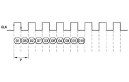
図3及び図4に示したように、本発明による差動ガンマデータ伝送方式は2データ/クロック伝送方式を用いて一つのクロック周期P間に2個の差動ガンマデータG1,G6を伝送する。すなわち、クロック信号の上昇エッジ(rising edge)では差動ガンマデータG1を伝送して、クロックの下降エッジ(falling edge)では差動ガンマデータG6を伝送する。その結果、TTL(transistor−transistor logic)信号に比べて速いデータ伝送速度を有するようになって、TTLデータバスに比べてバスの数を1/2に減らすようになる。また、差動ガンマデータを伝送する電圧の範囲は1.0〜1.2Vにすることが望ましい。 As shown in FIGS. 3 and 4, the differential gamma data transmission method according to the present invention transmits two differential gamma data G1 and G6 during one clock period P using a two data / clock transmission method. . That is, the differential gamma data G1 is transmitted at the rising edge of the clock signal, and the differential gamma data G6 is transmitted at the falling edge of the clock. As a result, the data transmission speed is higher than that of a TTL (transistor-transistor logic) signal, and the number of buses is reduced to ½ compared to the TTL data bus. The voltage range for transmitting differential gamma data is preferably 1.0-1.2V.
また、タイミング制御部500から提供する差動ガンマデータDgamは、対称的なパターン(symmetric pattern)、または非対称的なパターン(asymmetric pattern)でデータ駆動部400に伝送することができる。これはデータ駆動部400に差動ガンマデータDgamを伝送する形態をタイミング制御部500にプログラミングすることによって可能である。ここで、通常は、差動ガンマデータDgamを対称的なパターンで伝送して、液晶パネルに発生するキックバック電圧(kick back voltage)及び残像を考慮した場合には差動ガンマデータDgamを非対称的なパターンで伝送することができる。ここで、対称的なパターンは、たとえば、正極性及び負極性ガンマデータが同時に伝送されるものであって、非対称的なパターンは、たとえば、正極性または負極性ガンマデータが単独で伝送され、または正極性および負極性ガンマデータが同時に伝送されるものである。
In addition, the differential gamma data Dgam provided from the
図3に示すように、差動ガンマデータDgamを対称的なパターンでデータ駆動部400に伝送する場合、例えば、5ビットを用いて正極性及び負極性ガンマデータG1,G6を共にデータ駆動部400に伝達することができる。また、図4に示すように、差動ガンマデータDgamを非対称的なパターンでデータ駆動部400に伝送する場合、例えば、7ビットを用いて正極性ガンマデータG1,G2または負極性差動ガンマデータG6,G7を単独でデータ駆動部400に伝達し、または正極性ガンマデータG3及び負極性差動ガンマデータG8を共にデータ駆動部400に伝達することができる。ここで、差動ガンマデータはG1〜G10を用いており、G1、G2、G3、G4、G5は正極性ガンマデータを、G6、G7、G8、G9、G10は負極性ガンマデータをそれぞれ示す。
As shown in FIG. 3, when the differential gamma data Dgam is transmitted to the
図5は、本発明の一実施形態によるデータ駆動集積回路装置を示すブロック図である。 FIG. 5 is a block diagram illustrating a data driven integrated circuit device according to an embodiment of the present invention.
図5に示したように、本発明の一実施形態によるデータ駆動集積回路装置はタイミング制御部500から伝えられる差動ガンマデータDgamをデコーディングするガンマデコーディング部402とガンマデコーディング部402にそれぞれ連結されている複数のデジタルアナログ変換器DACとを含む変換部404、そして各デジタルアナログ変換器DACに連結されているバッファー部406を含む。
As shown in FIG. 5, the data driving integrated circuit device according to an exemplary embodiment of the present invention includes a
ガンマデコーディング部402は、複数個の比較器COMで構成されて、相互に対応する正極性ガンマデータDgamp及び負極性ガンマデータDgamnと基準電圧Vrefを入力に受けて最終入力された順序通りにデコーディングされた差動ガンマデータを出力する。例えば、ガンマデコーディング部402に入力された差動ガンマデータが5ビットといえば、ガンマデコーティング部402はデコーディングされた差動ガンマデータを順序通りG5からG1まで出力する。この時、基準電圧Vrefはアナログ電圧値を精密に調節する役割を果たし、駆動電圧AVDDの1/2に設定される。例えば、ガンマデコーディング部402から最初に出力される差動ガンマデータが7.8Vならば、この場合、基準電圧は3.9Vに設定される。ここで、基準電圧Vrefはデータ駆動集積回路装置の内部抵抗で具現されることができる。
The
各デジタル/アナログ変換器DACとバッファー(BUF)はガンマデコーディング部402から伝えられるデジタルデータをアナログ電圧値に変換及び増幅して出力する。このとき、バッファー(BUF)は電圧フォロワ(Voltage Follower)で形成することができる。ここでは、正極性及び負極性のアナログ電圧をそれぞれ5個ずつ、合わせて10個を生成することを例に挙げて説明しており、入力される差動ガンマデータDgam等によって生成されるアナログ電圧値の数はこれと異なる場合がある。
Each digital / analog converter DAC and a buffer (BUF) convert and amplify the digital data transmitted from the
以上、添付した図面を参照して本発明の実施形態を説明したが、本発明の属する技術分野における通常の知識を有する者は、本発明がその技術的思想や必須な特徴を変更しなくても他の具体的な形態で実施できるということを理解することができる。それゆえ上述した実施形態は全ての面で例示的なものであって限定的なものでないことに理解しなければならない。 The embodiments of the present invention have been described above with reference to the accompanying drawings. However, those who have ordinary knowledge in the technical field to which the present invention belongs need not change the technical idea and essential features of the present invention. It can be understood that the present invention can be implemented in other specific forms. Therefore, it should be understood that the above-described embodiments are illustrative in all aspects and not limiting.
本発明はデータ駆動集積回路装置とこれを含む液晶表示装置に適用されることである。 The present invention is applied to a data driven integrated circuit device and a liquid crystal display device including the same.
100 液晶パネル、
200 駆動電圧生成部、
300 ゲート駆動部、
400 データ駆動部、
500 タイミング制御部。
100 LCD panel,
200 drive voltage generator,
300 gate driver,
400 data driver,
500 Timing control unit.
Claims (18)
前記デコーディングされた差動ガンマデータをアナログ電圧値に変換するデジタル/アナログ変換部と、
前記アナログ電圧値を増幅して出力するバッファー部と、を含むことを特徴とするデータ駆動集積回路装置。 A gamma decoding unit that receives differential gamma data transmitted from the timing control unit at the input, decodes and outputs, and
A digital / analog converter for converting the decoded differential gamma data into an analog voltage value;
And a buffer unit for amplifying and outputting the analog voltage value.
ゲート駆動部及びデータ駆動集積回路装置を駆動するための信号を生成して、前記データ駆動集積回路装置に差動ガンマデータを提供するタイミング制御部と、
前記タイミング制御部から伝えられる差動ガンマデータをアナログ電圧値に変換して前記液晶パネルのデータ線に印加するデータ駆動集積回路装置と、を含むことを特徴とする液晶表示装置。 A liquid crystal panel including a plurality of thin film transistors, a plurality of gate lines connected to gate electrodes of the thin film transistors, and a plurality of data lines connected to source electrodes of the thin film transistors;
A timing controller for generating a signal for driving the gate driver and the data driving integrated circuit device, and providing differential gamma data to the data driving integrated circuit device;
And a data driving integrated circuit device for converting differential gamma data transmitted from the timing control unit into an analog voltage value and applying the analog voltage value to a data line of the liquid crystal panel.
前記デコーディングされた差動ガンマデータをアナログ電圧値に変換するデジタル/アナログ変換部と、
前記アナログ電圧値を増幅して出力するバッファー部と、を含むことを特徴とする請求項6に記載の液晶表示装置。 The data driving integrated circuit device includes a gamma decoding unit that receives differential gamma data transmitted from the timing control unit as input, decodes and outputs the differential gamma data,
A digital / analog converter for converting the decoded differential gamma data into an analog voltage value;
The liquid crystal display device according to claim 6, further comprising: a buffer unit that amplifies and outputs the analog voltage value.
Applications Claiming Priority (1)
| Application Number | Priority Date | Filing Date | Title |
|---|---|---|---|
| KR1020050115849A KR20070056779A (en) | 2005-11-30 | 2005-11-30 | Data drive integrated circuit device and liquid crystal display device comprising the same |
Publications (2)
| Publication Number | Publication Date |
|---|---|
| JP2007156419A true JP2007156419A (en) | 2007-06-21 |
| JP2007156419A5 JP2007156419A5 (en) | 2009-09-24 |
Family
ID=38086942
Family Applications (1)
| Application Number | Title | Priority Date | Filing Date |
|---|---|---|---|
| JP2006221659A Pending JP2007156419A (en) | 2005-11-30 | 2006-08-15 | Data driving integrated circuit device and liquid crystal display device including the same |
Country Status (3)
| Country | Link |
|---|---|
| US (1) | US20070120805A1 (en) |
| JP (1) | JP2007156419A (en) |
| KR (1) | KR20070056779A (en) |
Families Citing this family (14)
| Publication number | Priority date | Publication date | Assignee | Title |
|---|---|---|---|---|
| US8421722B2 (en) * | 2006-12-04 | 2013-04-16 | Himax Technologies Limited | Method of transmitting data from timing controller to source driving device in LCD |
| KR100866603B1 (en) * | 2007-01-03 | 2008-11-03 | 삼성전자주식회사 | Data processing method and apparatus for performing deserializing and serializing |
| KR101362154B1 (en) * | 2007-06-11 | 2014-02-13 | 엘지디스플레이 주식회사 | Liquid crystal display device |
| US8184078B2 (en) * | 2008-12-03 | 2012-05-22 | Himax Media Solutions, Inc. | Liquid crystal display and source driving circuit having a gamma and common voltage generator thereof |
| US20100141636A1 (en) * | 2008-12-09 | 2010-06-10 | Stmicroelectronics Asia Pacific Pte Ltd. | Embedding and transmitting data signals for generating a display panel |
| JP5241036B2 (en) * | 2009-07-07 | 2013-07-17 | ルネサスエレクトロニクス株式会社 | Liquid crystal display driver and liquid crystal display device |
| GB2495607B (en) * | 2011-10-11 | 2014-07-02 | Lg Display Co Ltd | Liquid crystal display device and driving method thereof |
| CN103021352B (en) * | 2012-09-28 | 2014-08-20 | 合肥京东方光电科技有限公司 | Liquid crystal panel driving method |
| KR102130142B1 (en) | 2013-12-31 | 2020-07-06 | 엘지디스플레이 주식회사 | Curcuit for Generating Gamma Voltage and Display Panel having the Same |
| CN109817178B (en) * | 2019-03-22 | 2021-06-11 | 重庆惠科金渝光电科技有限公司 | Gamma circuit, driving circuit and display device |
| TWI709129B (en) * | 2019-12-18 | 2020-11-01 | 敦泰電子股份有限公司 | Extended gamma device of display panel and display device having the same |
| CN111556614B (en) * | 2020-05-09 | 2021-06-01 | 深圳市华星光电半导体显示技术有限公司 | Data processing method of driving circuit and driving circuit |
| CN114373415A (en) * | 2020-10-15 | 2022-04-19 | 元太科技工业股份有限公司 | Display device |
| TWI751737B (en) * | 2020-10-15 | 2022-01-01 | 元太科技工業股份有限公司 | Display apparatus |
Family Cites Families (5)
| Publication number | Priority date | Publication date | Assignee | Title |
|---|---|---|---|---|
| US6144354A (en) * | 1996-06-20 | 2000-11-07 | Seiko Epson Corporation | Image display apparatus |
| JP2001195031A (en) * | 1999-10-27 | 2001-07-19 | Internatl Business Mach Corp <Ibm> | Reference potential generating circuit for gamma correction |
| KR100359433B1 (en) * | 2000-07-27 | 2002-11-23 | 삼성전자 주식회사 | Flat panel display apparatus |
| JP4221183B2 (en) * | 2002-02-19 | 2009-02-12 | 株式会社日立製作所 | Liquid crystal display |
| KR100900548B1 (en) * | 2002-12-17 | 2009-06-02 | 삼성전자주식회사 | Liquid crystal display for generating common voltages with different values |
-
2005
- 2005-11-30 KR KR1020050115849A patent/KR20070056779A/en not_active Application Discontinuation
-
2006
- 2006-08-15 JP JP2006221659A patent/JP2007156419A/en active Pending
- 2006-11-15 US US11/560,135 patent/US20070120805A1/en not_active Abandoned
Also Published As
| Publication number | Publication date |
|---|---|
| US20070120805A1 (en) | 2007-05-31 |
| KR20070056779A (en) | 2007-06-04 |
Similar Documents
| Publication | Publication Date | Title |
|---|---|---|
| JP2007156419A (en) | Data driving integrated circuit device and liquid crystal display device including the same | |
| KR101361083B1 (en) | Data driving apparatus, liquid crystal display comprising the same and method for driving of liquid crystal display | |
| JP5348582B2 (en) | Liquid crystal display | |
| US20150325200A1 (en) | Source driver and display device including the same | |
| US7663586B2 (en) | Reference voltage generation circuit, display driver, electro-optical device, and electronic instrument | |
| KR101639308B1 (en) | Method of driving display panel and display apparatus for performing the method | |
| JP4466710B2 (en) | Electro-optical device and electronic apparatus | |
| KR100736143B1 (en) | Auto digital variable resistor and liquid crystal display comprising the same | |
| US20050243049A1 (en) | Semiconductor integrated circuit device | |
| JP3726910B2 (en) | Display driver and electro-optical device | |
| JP2004240428A (en) | Liquid crystal display, device and method for driving liquid crystal display | |
| JP2007065135A (en) | Liquid crystal display device | |
| KR20020003805A (en) | Liquid crystal display device | |
| JP3748904B2 (en) | Liquid crystal display | |
| JP2007219091A (en) | Driving circuit, electrooptical device, and electronic equipment | |
| US7843474B2 (en) | Driving apparatus for liquid crystal display | |
| KR101313650B1 (en) | Circuit for compensating clock signal of liquid crystal display | |
| JP2003223148A (en) | Method for driving liquid crystal display device and liquid crystal display device | |
| KR20070066194A (en) | Display apparatus | |
| KR100989244B1 (en) | Liquid crystal display device and dirving method thereof | |
| JP3837153B2 (en) | Liquid crystal display | |
| JP2004061985A (en) | Drive circuit for liquid crystal display | |
| KR20070083001A (en) | Driving apparatus and liquid crystal display comprising the same | |
| KR20050068535A (en) | The driving circuit of the liquid crystal display device | |
| KR20070045729A (en) | Auto digital variable resistor and liquid crystal display comprising the same |
Legal Events
| Date | Code | Title | Description |
|---|---|---|---|
| A521 | Written amendment |
Free format text: JAPANESE INTERMEDIATE CODE: A523 Effective date: 20090811 |
|
| A621 | Written request for application examination |
Free format text: JAPANESE INTERMEDIATE CODE: A621 Effective date: 20090811 |
|
| A072 | Dismissal of procedure [no reply to invitation to correct request for examination] |
Free format text: JAPANESE INTERMEDIATE CODE: A073 Effective date: 20110208 |