JP4466710B2 - Electro-optical device and electronic apparatus - Google Patents
Electro-optical device and electronic apparatus Download PDFInfo
- Publication number
- JP4466710B2 JP4466710B2 JP2007260619A JP2007260619A JP4466710B2 JP 4466710 B2 JP4466710 B2 JP 4466710B2 JP 2007260619 A JP2007260619 A JP 2007260619A JP 2007260619 A JP2007260619 A JP 2007260619A JP 4466710 B2 JP4466710 B2 JP 4466710B2
- Authority
- JP
- Japan
- Prior art keywords
- lines
- signal
- data
- image signal
- line
- Prior art date
- Legal status (The legal status is an assumption and is not a legal conclusion. Google has not performed a legal analysis and makes no representation as to the accuracy of the status listed.)
- Expired - Fee Related
Links
Images


Classifications
-
- G—PHYSICS
- G09—EDUCATION; CRYPTOGRAPHY; DISPLAY; ADVERTISING; SEALS
- G09G—ARRANGEMENTS OR CIRCUITS FOR CONTROL OF INDICATING DEVICES USING STATIC MEANS TO PRESENT VARIABLE INFORMATION
- G09G3/00—Control arrangements or circuits, of interest only in connection with visual indicators other than cathode-ray tubes
- G09G3/20—Control arrangements or circuits, of interest only in connection with visual indicators other than cathode-ray tubes for presentation of an assembly of a number of characters, e.g. a page, by composing the assembly by combination of individual elements arranged in a matrix no fixed position being assigned to or needed to be assigned to the individual characters or partial characters
- G09G3/34—Control arrangements or circuits, of interest only in connection with visual indicators other than cathode-ray tubes for presentation of an assembly of a number of characters, e.g. a page, by composing the assembly by combination of individual elements arranged in a matrix no fixed position being assigned to or needed to be assigned to the individual characters or partial characters by control of light from an independent source
- G09G3/36—Control arrangements or circuits, of interest only in connection with visual indicators other than cathode-ray tubes for presentation of an assembly of a number of characters, e.g. a page, by composing the assembly by combination of individual elements arranged in a matrix no fixed position being assigned to or needed to be assigned to the individual characters or partial characters by control of light from an independent source using liquid crystals
- G09G3/3611—Control of matrices with row and column drivers
- G09G3/3685—Details of drivers for data electrodes
- G09G3/3688—Details of drivers for data electrodes suitable for active matrices only
-
- G—PHYSICS
- G09—EDUCATION; CRYPTOGRAPHY; DISPLAY; ADVERTISING; SEALS
- G09G—ARRANGEMENTS OR CIRCUITS FOR CONTROL OF INDICATING DEVICES USING STATIC MEANS TO PRESENT VARIABLE INFORMATION
- G09G3/00—Control arrangements or circuits, of interest only in connection with visual indicators other than cathode-ray tubes
- G09G3/20—Control arrangements or circuits, of interest only in connection with visual indicators other than cathode-ray tubes for presentation of an assembly of a number of characters, e.g. a page, by composing the assembly by combination of individual elements arranged in a matrix no fixed position being assigned to or needed to be assigned to the individual characters or partial characters
- G09G3/34—Control arrangements or circuits, of interest only in connection with visual indicators other than cathode-ray tubes for presentation of an assembly of a number of characters, e.g. a page, by composing the assembly by combination of individual elements arranged in a matrix no fixed position being assigned to or needed to be assigned to the individual characters or partial characters by control of light from an independent source
- G09G3/36—Control arrangements or circuits, of interest only in connection with visual indicators other than cathode-ray tubes for presentation of an assembly of a number of characters, e.g. a page, by composing the assembly by combination of individual elements arranged in a matrix no fixed position being assigned to or needed to be assigned to the individual characters or partial characters by control of light from an independent source using liquid crystals
-
- G—PHYSICS
- G09—EDUCATION; CRYPTOGRAPHY; DISPLAY; ADVERTISING; SEALS
- G09G—ARRANGEMENTS OR CIRCUITS FOR CONTROL OF INDICATING DEVICES USING STATIC MEANS TO PRESENT VARIABLE INFORMATION
- G09G2300/00—Aspects of the constitution of display devices
- G09G2300/04—Structural and physical details of display devices
- G09G2300/0421—Structural details of the set of electrodes
- G09G2300/0426—Layout of electrodes and connections
-
- G—PHYSICS
- G09—EDUCATION; CRYPTOGRAPHY; DISPLAY; ADVERTISING; SEALS
- G09G—ARRANGEMENTS OR CIRCUITS FOR CONTROL OF INDICATING DEVICES USING STATIC MEANS TO PRESENT VARIABLE INFORMATION
- G09G2310/00—Command of the display device
- G09G2310/02—Addressing, scanning or driving the display screen or processing steps related thereto
- G09G2310/0264—Details of driving circuits
- G09G2310/0297—Special arrangements with multiplexing or demultiplexing of display data in the drivers for data electrodes, in a pre-processing circuitry delivering display data to said drivers or in the matrix panel, e.g. multiplexing plural data signals to one D/A converter or demultiplexing the D/A converter output to multiple columns
-
- G—PHYSICS
- G09—EDUCATION; CRYPTOGRAPHY; DISPLAY; ADVERTISING; SEALS
- G09G—ARRANGEMENTS OR CIRCUITS FOR CONTROL OF INDICATING DEVICES USING STATIC MEANS TO PRESENT VARIABLE INFORMATION
- G09G2310/00—Command of the display device
- G09G2310/08—Details of timing specific for flat panels, other than clock recovery
Landscapes
- Engineering & Computer Science (AREA)
- Chemical & Material Sciences (AREA)
- Crystallography & Structural Chemistry (AREA)
- Physics & Mathematics (AREA)
- Computer Hardware Design (AREA)
- General Physics & Mathematics (AREA)
- Theoretical Computer Science (AREA)
- Control Of Indicators Other Than Cathode Ray Tubes (AREA)
- Liquid Crystal Display Device Control (AREA)
- Liquid Crystal (AREA)
- Devices For Indicating Variable Information By Combining Individual Elements (AREA)
Description
本発明は、画像信号線に供給されるデータ線をデータ線にサンプリングさせる構成にお
いて配線形成に必要な領域を抑える技術に関する。
The present invention relates to a technique for suppressing a region necessary for wiring formation in a configuration in which data lines supplied to image signal lines are sampled by data lines.
液晶などの電気光学装置では、走査線とデータ線との交差に対応して画素が設けられ、
当該画素が、走査線が選択されたときにデータ線に供給されたデータ信号の電圧に応じた
明るさ(階調)となる構成となっている。このような構成において駆動方式で大別すると
、デジタル駆動式とアナログ駆動式とに分けることができるが、現時点においてアナログ
駆動式が広く用いられている。
このようなアナログ駆動式においては、さらにデマルチプレクサ式とブロック順次式と
が多く用いられている。このうち、ブロック順次式では、データ線を予め定められた列数
、例えば6列毎にブロック化して、ある走査線が選択される期間において、ブロックを順
番に選択し、6本の画像信号線に供給されたデータ信号を、選択したブロックに属する6
列のデータ線に同時にサンプリングして供給する、という方式である(特許文献1参照)
。
The pixel is configured to have brightness (gradation) corresponding to the voltage of the data signal supplied to the data line when the scanning line is selected. In such a configuration, the driving method can be roughly divided into a digital driving method and an analog driving method. At present, the analog driving method is widely used.
In such an analog drive type, a demultiplexer type and a block sequential type are more frequently used. Among these, in the block sequential type, the data lines are divided into a predetermined number of columns, for example, every six columns, and in a period in which a certain scanning line is selected, the blocks are selected in order, and six image signal lines are selected. The data signal supplied to is assigned to the
This is a method of sampling and supplying data to the data lines in the column simultaneously (see Patent Document 1).
.
ところで、このブロック順次式では、複数本の画像信号線の引き回しに難点があった。
詳細には、接続端子の位置によっては、画像信号線の引き回しに広いスペースが必要とな
り、表示領域外のいわゆる額縁領域の狭小化を阻む大きな要因の1つとなった。
本発明は、上述した事情に鑑みてなされたもので、その目的の1つは、ブロック順次式
において額縁領域の狭小化を図ることが可能な電気光学装置および電子機器を提供するこ
とにある。
However, in this block sequential type, there is a difficulty in routing a plurality of image signal lines.
Specifically, depending on the position of the connection terminal, a large space is required for routing the image signal line, which is one of the major factors that prevent the so-called frame area outside the display area from being narrowed.
SUMMARY An advantage of some aspects of the invention is that it provides an electro-optical device and an electronic apparatus capable of narrowing a frame area in a block sequential manner.
上記目的を達成するために本発明に係る電気光学装置にあっては、複数の走査線と、複
数m本の画像信号線と、前記m本の画像信号線の各々と対をなすように設けられ、各々は
、それぞれ対をなす画像信号線に接続されて、データ信号を供給するm本の接続信号線と
、m本毎にブロック化されたデータ線であって、一つのブロックにおけるm本のデータ線
は、前記m本の画像信号線のそれぞれと対をなすように設けられた複数のデータ線と、前
記複数の走査線を所定の順番で選択する走査線駆動回路と、一本の走査線に選択される期
間にわたって、前記ブロックの選択を示すサンプリング信号を所定の順番で出力するブロ
ック選択回路と、前記複数のデータ線のそれぞれに設けられ、各々は、前記サンプリング
信号がブロックの選択を示すときに、対をなす画像信号線とデータ線との間でオン状態と
なるサンプリングスイッチと、前記複数の走査線と前記複数のデータ線との交差に対応し
て設けられ、各々は、前記走査線が選択されたときに、前記データ線にサンプリングされ
たデータ信号に応じた階調となる画素と、を備え、前記ブロック選択回路は、出力端が次
段の入力端に接続された単位回路を複数個有し、前記複数個の単位回路の各々は、前記入
力端に供給されたパルスを所定時間遅延させて出力端から出力するとともに、入力端およ
び出力端に供給されたパルスに基づいてサンプリング信号を出力し、前記接続信号線は、
一の単位回路の出力端と次段の単位回路の入力端との間を結ぶ連絡信号線と交差するよう
に設けられていることを特徴とする。本発明によれば、m本の画像信号線は、m本の連絡
信号線によってブロック選択回路を回り込ませる必要がなくなるので、その分のスペース
が不要となり、額縁の狭小化を図ることができる。
In order to achieve the above object, the electro-optical device according to the present invention is provided so as to be paired with a plurality of scanning lines, a plurality of m image signal lines, and each of the m image signal lines. Each of which is connected to a pair of image signal lines to supply data signals, and m connection signal lines for supplying data signals, and m data lines that are blocked every m lines. The data lines include a plurality of data lines provided in pairs with the m image signal lines, a scanning line driving circuit for selecting the plurality of scanning lines in a predetermined order, and a single data line. Provided in each of the plurality of data lines and a block selection circuit that outputs a sampling signal indicating selection of the block in a predetermined order over a period selected by the scanning line, and each of the sampling signals is a block selection Indicate And a sampling switch that is turned on between the paired image signal line and the data line, and corresponding to the intersection of the plurality of scanning lines and the plurality of data lines, And a pixel having a gradation corresponding to a data signal sampled on the data line, and the block selection circuit includes a unit circuit whose output terminal is connected to the input terminal of the next stage. Each of the plurality of unit circuits delays a pulse supplied to the input terminal by a predetermined time and outputs it from the output terminal, and samples based on the pulses supplied to the input terminal and the output terminal. The signal is output, and the connection signal line is
It is provided so as to intersect with a communication signal line connecting between the output terminal of one unit circuit and the input terminal of the next unit circuit. According to the present invention, the m image signal lines do not need to be routed around the block selection circuit by the m communication signal lines, so that the corresponding space is not required, and the frame can be narrowed.
本発明において、前記m本の画像信号線は、前記複数のデータ線の延長線と交差する方
向に設けられ、前記単位回路の配列方向は、前記m本の画像信号線が設けられる方向に一
致する構成が好ましい。また、本発明において、前記m本の接続信号線が、同一の連絡信
号線とそれぞれ交差するように設けられた構成としても良い。
本発明において、前記画素は、n(nは3以上の整数)色のうち、いずれかであり、前
記mはnの倍数であり、一つのブロックに属するm本のデータ線は、前記n色の画素に対
応するものが所定の順番で繰り返して配列し、前記m本の画像信号線は、前記m本のデー
タ線における色と同じ順番で繰り返して配列し、同色に対応する画像信号線に接続された
m/n本の接続信号線が、少なくとも同一の連絡信号線と交差するように設けられた構成
としても良い。この構成によれば、接続信号線の時定数を色毎に揃えることが可能となる
。
本発明において、前記画素は、n(nは3以上の整数)色のうち、いずれかであり、前
記mはnの倍数であり、一つブロックに属するm本のデータ線は、前記n色の画素に対応
するものが所定の順番で繰り返して配列し、前記m本の画像信号線は、前記m/n本毎に
まとまってデータ線の色と同じ順番で配列し、同色に対応する画像信号線に接続されたm
/n本の接続信号線が、同一の連絡信号線と交差するように設けられた構成としても良い
。この構成によれば、接続信号線にくわえて、画像信号線の時定数についても色毎に揃え
ることが可能となる。
なお、本発明は、電気光学装置のみならず、当該電気光学装置を有する電子機器として
も概念することが可能である。
In the present invention, the m image signal lines are provided in a direction intersecting with an extension line of the plurality of data lines, and an arrangement direction of the unit circuits is coincident with a direction in which the m image signal lines are provided. The structure which does is preferable. In the present invention, the m connection signal lines may be provided so as to intersect with the same connection signal line.
In the present invention, the pixel is one of n (n is an integer of 3 or more) colors, m is a multiple of n, and m data lines belonging to one block are the n colors. Corresponding to the pixels are repeatedly arranged in a predetermined order, and the m image signal lines are repeatedly arranged in the same order as the colors of the m data lines, and the image signal lines corresponding to the same color are arranged. A configuration may be adopted in which the connected m / n connection signal lines cross at least the same connection signal line. According to this configuration, it is possible to align the time constant of the connection signal line for each color.
In the present invention, the pixel is one of n (n is an integer of 3 or more) colors, m is a multiple of n, and m data lines belonging to one block are the n colors. Are arranged repeatedly in a predetermined order, and the m image signal lines are arranged in the same order as the color of the data lines together for each of the m / n lines, and images corresponding to the same color are arranged. M connected to signal line
/ N connection signal lines may be provided so as to intersect with the same connection signal line. According to this configuration, in addition to the connection signal line, the time constant of the image signal line can be made uniform for each color.
The present invention can be conceptualized not only as an electro-optical device but also as an electronic apparatus having the electro-optical device.
以下、本発明の実施形態について図面を参照して説明する。
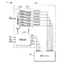
図1は、本発明の第1実施形態に係る電気光学装置の全体構成を示すブロック図である
。この図に示されるように、電気光学装置1は、表示パネル10と処理回路20とに大別
される。このうち、処理回路20は、表示パネル10とは、例えばFPC(flexible pri
nted circuit)基板によって接続される回路モジュールである。
Embodiments of the present invention will be described below with reference to the drawings.
FIG. 1 is a block diagram showing the overall configuration of the electro-optical device according to the first embodiment of the invention. As shown in this figure, the electro-
nted circuit) is a circuit module connected by a substrate.
処理回路20は、制御回路210、S/P変換回路220およびD/A変換回路群23
0を含む。このうち、制御回路210は、外部上位回路(図示省略)から垂直同期信号V
s、水平同期信号Hsおよびドットクロック信号Dclkに同期して、S/P変換回路220
の動作を制御したり、D/A変換回路群230における変換極性を指定したり、表示パネ
ル10の動作を制御するためのスタートパルスDX、DY、クロック信号CLX、CLY
等を出力したりするものである。なお、図1では、省略しているが、制御回路210は、
クロック信号CLXの論理反転させた反転クロック信号CLXinv、および、クロック信
号CLYの論理反転させた反転クロック信号CLYinvも表示パネル10に出力する。
The
Contains zero. Among these, the
s, the S /
Start pulses DX, DY, clock signals CLX, CLY for controlling the operation of the display panel, designating the conversion polarity in the D / A
Or the like. Although not shown in FIG. 1, the
An inverted clock signal CLXinv obtained by logically inverting the clock signal CLX and an inverted clock signal CLYinv obtained by logically inverting the clock signal CLY are also output to the
S/P変換回路220は、垂直同期信号Vs、水平同期信号Hsおよびドットクロック信
号Dclkに同期して供給されるデジタルの画像データVdを、後述するように6チャネルに
分配するとともに、1ドット分を時間軸に2倍に伸長して(シリアル−パラレル変換、相
展開という場合もある)、それぞれ画像データVd1d〜Vd6dとして出力するものである。
ここで、画像データVdは、1ドットについてR(赤)、G(緑)、B(青)の各色成
分の階調(明るさ)をそれぞれで指定するものである。S/P変換回路220では、画像
データVdで指定されるドットのうち、奇数列ドットのR、G、Bの階調を指定するもの
がそれぞれ画像データVd1d、Vd2d、Vd3dに分配され、当該奇数列に続く偶数列ドット
のR、G、Bの階調を指定するものがそれぞれ画像データVd4d、Vd5d、Vd6dに分配さ
れる。
The S /
Here, the image data Vd specifies the gradation (brightness) of each color component of R (red), G (green), and B (blue) for each dot. In the S /
D/A変換回路群230は、チャネル毎に設けられたD/A変換回路の集合体であり、
画像データVd1d〜Vd6dを、それぞれ制御回路210によって指定された極性の電圧に変
換して、データ信号Vid1〜Vid6として出力する。
ここで、データ信号Vid1〜Vid6の極性とは、電圧Vcに対して高位側を正極性とし、
低位側を負極性とする。なお、電圧Vcとは、後述する図8に示されるようにHレベルに
相当する選択電圧Vddと、Lレベルに相当し、かつ電圧の基準である電位Gnd(電圧ゼロ
)とのほぼ中間電圧である。
また、データ信号Vid1、Vid2、Vid3は、奇数列ドットのうち、それぞれR、G、B
の階調に応じた電圧の信号であるから、R1、G1、B1と表記することにする。同様に、
データ信号Vid4、Vid5、Vid6は、偶数列ドットのうち、それぞれR、G、Bの階調に
応じた電圧の信号であるから、R2、G2、B2と表記することにする。
The D / A
The image data Vd1d to Vd6d are converted into voltages having polarities designated by the
Here, the polarity of the data signals Vid1 to Vid6 means that the higher side with respect to the voltage Vc is positive.
The lower side is negative. The voltage Vc is an almost intermediate voltage between the selection voltage Vdd corresponding to the H level and the potential Gnd (voltage zero) which corresponds to the L level and is a voltage reference, as shown in FIG. is there.
The data signals Vid1, Vid2, and Vid3 are R, G, and B of odd-numbered dots, respectively.
Since it is a signal of a voltage corresponding to the gray scale, it is expressed as R1, G1, B1. Similarly,
Since the data signals Vid4, Vid5, and Vid6 are signals of voltages corresponding to the R, G, and B gradations of the even-numbered dots, they are expressed as R2, G2, and B2.
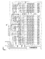
次に、表示パネル10の構成について説明する。図2は、表示パネル10の構成を示す
平面図である。
表示パネル10は、液晶を用いて所定の表示を行うものであり、表示領域100の周辺
に、走査線駆動回路130や、ブロック選択回路142、画像信号線170、サンプリン
グ回路146などが配置した周辺回路内蔵型となっている。
表示領域100は、画素110が配列する領域であり、本実施形態では、480行の走
査線112が横方向(X方向)に設けられる一方、1920(=640×3)列のデータ
線114が図において縦方向(Y方向)に設けられている。そして、これらの走査線11
2とデータ線114との交差の各々に対応するように画素110がそれぞれ設けられてい
る。
Next, the configuration of the
The
The
ここで、画素110は、1列毎にR(赤)、G(緑)、B(青)に対応して配列してお
り、これらのX方向で互いに隣接するR、G、Bの3画素で1ドットのカラーを表現する
。したがって、本実施形態では、表示領域100において画素110を単位としてみると
縦480行×横1920列でマトリクス状に配列し、カラー表示の単位であるドットでみ
ると、縦480行×横640列で配列することになるが、本発明をこの配列に限定する趣
旨ではない。
また、1〜1920列のデータ線114は、本実施形態では隣接する6列毎にブロック
化されている。本実施形態においてデータ線114の列数は「1920」であるので、ブ
ロック数は「320」となる。
Here, the
Further, the
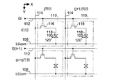
次に、画素110について説明する。
図3は、画素110の構成を示す図であり、i行及びこれに下方向で隣接する(i+1
)行と、j列及びこれに右方向で隣接する(j+1)列との交差に対応する2×2の計4
画素分の構成が示されている。なお、i、(i+1)は、画素110が配列する行を一般
的に示す場合の記号であって、本実施形態では、それぞれ1以上480以下を満たす整数
であり、j、(j+1)は、画素110が配列する列を一般的に示す場合の記号であって
、本実施形態では、それぞれ1以上1920以下を満たす整数である。
Next, the
FIG. 3 is a diagram illustrating a configuration of the
) 2 × 2 total 4 corresponding to the intersection of the row and j column and (j + 1) column adjacent to it in the right direction
A configuration for pixels is shown. Note that i and (i + 1) are symbols for generally indicating the row in which the
図3に示されるように、各画素110は、nチャネル型の薄膜トランジスタ(thin fil
m transistor:以下単に「TFT」と略称する)116と、液晶素子120とを有する。
各画素110については、本実施形態では電気的には互いに同一構成なので、i行j列に
位置するもので代表して説明すると、当該i行j列の画素110において、TFT116
のゲート電極はi行目の走査線112に接続される一方、そのソース電極はj列目のデー
タ線114に接続され、そのドレイン電極は画素電極118に接続されている。
As shown in FIG. 3, each
m transistor: hereinafter simply abbreviated as “TFT”) 116 and a
Since each
The gate electrode is connected to the i-
表示パネル10は、特に図示しないが、素子基板と対向基板との一対の基板が一定の間
隙を保って貼り合わせられるとともに、この間隙に液晶105が封止された構成となって
いる。このうち、素子基板には、走査線112や、データ線114、TFT116、画素
電極118などが形成される一方、対向基板にコモン電極108が形成されて、これらの
電極形成面が互いに対向するように一定の間隙を保って貼り合わせられている。このため
、本実施形態において液晶素子120は、画素電極118とコモン電極108とが液晶1
05を挟持することによって構成されることになる。コモン電極108には、本実施形態
では、時間的に一定の電圧LCcomが印加されている。
Although not particularly shown, the
It is configured by sandwiching 05. In this embodiment, a constant voltage LCcom is applied to the
なお、本実施形態では、液晶素子120を透過型とした場合、透過光量を着色するカラ
ーフィルタ(図示省略)が設けられる。ここで、画素電極118とコモン電極108との
間を通過する光の透過率は、液晶素子に保持される電圧の実効値がゼロであれば最小値(
最も暗い状態)となる一方、当該実効値が大きくなるにつれて、透過率が徐々に大きくな
るノーマリーブラックモードに設定される。このため、バックライトユニット(図示省略
)よって照射された光は、画素毎に、液晶素子120に保持された電圧の実効値に応じた
比率でカラーフィルタにより着色して出射する。
In the present embodiment, when the
On the other hand, the normally black mode in which the transmittance gradually increases as the effective value increases is set. For this reason, the light irradiated by the backlight unit (not shown) is emitted by being colored by the color filter at a ratio corresponding to the effective value of the voltage held in the
ところで、素子基板において、表示領域100の外側であってY方向に沿った一辺に沿
って走査線駆動回路130が設けられる一方、X方向に沿った一辺には、内側の表示領域
100に向かって順番に、ブロック選択回路142、画像信号線170、サンプリング回
路146が設けられている。
Meanwhile, in the element substrate, the scanning
走査線駆動回路130は、垂直走査期間(F)のうち、垂直走査有効期間(Fa)にわ
たって走査信号Y1、Y2、Y3、…、Y480を、それぞれ1、2、3、…、480行目の走
査線112に供給するものである。詳細には、走査線駆動回路130は、走査線112を
1、2、3、…、480行目という順番で水平走査期間(H)毎に選択し、図5に示され
るように、選択した走査線への走査信号をHレベルに相当する選択電圧Vddとし、他の走
査線への走査信号をLレベルに相当する接地電位Gndとする。
なお、図5では、垂直走査期間(F)のうち、垂直走査有効期間(Fa)以外を垂直走
査帰線期間(Fb)として表記している。
The scanning
In FIG. 5, the vertical scanning period (F) other than the vertical scanning effective period (Fa) is represented as a vertical scanning blanking period (Fb).
ブロック選択回路142は、単位回路144を、データ線114におけるブロック総数
である「320」個、走査線112の配列方向であるX方向に沿って縦続接続したもので
ある。詳細には、図2において左から数えて1段目の単位回路144には、入力信号とし
て、処理回路20(制御回路210)からのスタートパルスDYが供給される一方、当該
1段目の単位回路144の出力信号は、連絡信号線181を介して2段目の単位回路14
4の入力信号として転送され、以下同様に、ある段の単位回路144の出力信号が、次段
の単位回路144の入力信号として転送される関係にある。
The
In the same manner, the output signal of the
ここで、単位回路144の詳細について説明する。図4は、単位回路144の構成を示
す回路図である。
奇数段目および偶数段目の単位回路144は、いずれもクロックドインバータ151、
153と、インバータ152、155と、NAND回路154とを有する。ここで、各段
目の単位回路144の入力端は、クロックドインバータ151の入力端であり、単位回路
144の出力端は、インバータ152の出力端である。便宜的に、1、2、3、4、…、
320段目の単位回路144における出力端から出力される信号を、それぞれn1、n2、
n3、n4、…、n320と表記する。
Here, details of the
The odd-numbered and even-numbered
153,
Signals output from the output terminals of the
n3, n4,..., n320.
奇数段目の単位回路144において、クロックドインバータ151は、クロック信号C
LXがHレベルであるときに(反転クロック信号CLXinvがLレベルであるときに)入
力端に供給された信号を論理反転した否定信号を出力端に出力し、クロック信号CLXが
Lレベルであるときに(反転クロック信号CLXinvがHレベルであるときに)出力端を
ハイ・インピーダンス状態とするものであり、その出力端は、インバータ152の入力端
に接続されている。インバータ152は、入力端に供給された信号の否定信号を出力端に
出力するものである。インバータの152の出力端は、クロックドインバータ153の入
力端に接続されている。奇数段目の単位回路144において、クロックドインバータ15
3は、反転クロック信号CLXinvがHレベルであるときに(クロック信号CLXがLレ
ベルであるときに)入力端に供給された信号を論理反転した否定信号を出力端に出力し、
反転クロック信号CLXinvがLレベルであるときに(クロック信号CLXがHレベルで
あるときに)出力端をハイ・インピーダンス状態とするものであり、その出力端は、イン
バータ152の入力端に接続されている。
一方、NAND回路154は、単位回路144の入力端に供給された信号と出力端に供
給された信号との否定論理積信号を出力し、インバータ155は、当該否定論理積信号の
論理を再反転して、サンプリング信号として出力する。したがって、ある段について着目
した場合に、当該着目段のサンプリング信号は、当該着目段の単位回路144における入
力端信号および出力端信号の論理積信号となる。
In the odd-numbered
When LX is at the H level (when the inverted clock signal CLXinv is at the L level), a negative signal obtained by logically inverting the signal supplied to the input terminal is output to the output terminal, and when the clock signal CLX is at the L level (When the inverted clock signal CLXinv is at the H level), the output terminal is set to a high impedance state, and the output terminal is connected to the input terminal of the
3 outputs to the output terminal a negative signal obtained by logically inverting the signal supplied to the input terminal when the inverted clock signal CLXinv is at the H level (when the clock signal CLX is at the L level),
When the inverted clock signal CLXinv is at L level (when the clock signal CLX is at H level), the output terminal is set to a high impedance state, and the output terminal is connected to the input terminal of the
On the other hand, the
なお、偶数段目の単位回路144については、クロックドインバータ151、153の
機能が奇数段目と逆転した関係にある点以外、同一構成である。すなわち、偶数段目にお
いてクロックドインバータ151は、反転クロック信号CLXinvがHレベルであるとき
に否定信号を出力し、反転クロック信号CLXinvがLレベルであるときに出力端がハイ
・インピーダンス状態となり、また、クロックドインバータ153は、クロック信号CL
XがHレベルであるときに否定信号を出力し、クロック信号CLXがLレベルであるとき
に出力端がハイ・インピーダンス状態となり、他については偶数段目と同構成である。
Note that the even-numbered
When X is at the H level, a negative signal is output, and when the clock signal CLX is at the L level, the output terminal is in a high impedance state.
このような構成において、クロック信号CLXがHレベルである(反転クロック信号C
LXinvがLレベルである)とき、奇数段目の単位回路144におけるクロックドインバ
ータ153の出力端がハイ・インピーダンス状態となるので、奇数段目の単位回路144
の入力端に供給された信号は、当該奇数段目のクロックドインバータ151、および、イ
ンバータ152による2回の論理反転により正転して当該奇数段の単位回路144の出力
信号として出力される。
次に、クロック信号CLXがLレベルとなった(反転クロック信号CLXinvがHレベ
ルとなった)とき、奇数段目におけるクロックドインバータ151の出力端がハイ・イン
ピーダンス状態となるので、インバータ152による出力信号(奇数段目の単位回路の出
力信号)は、インバータ152およびクロックドインバータ153によるラッチによって
、クロック信号CLXがLレベルとなる直前の論理レベルに保持される一方、この保持さ
れた信号が偶数段目の単位回路144の入力端に供給されて、当該偶数段目のクロックド
インバータ151、および、インバータ152による2回の論理反転により正転して当該
偶数段の単位回路144の出力信号として出力される。
このような動作が、クロック信号CLX(反転クロック信号CLXinv)の論理レベル
が変化する毎に実行されるので、1、2、3、…、320段目の単位回路144による出
力信号は、クロック信号CLXが反転する毎にシフトした関係となる。
In such a configuration, the clock signal CLX is at the H level (inverted clock signal C
LXinv is at the L level), the output terminal of the clocked
The signal supplied to the input terminal of the odd-numbered stage is forwardly rotated by two logic inversions by the odd-numbered clocked
Next, when the clock signal CLX becomes the L level (the inverted clock signal CLXinv becomes the H level), the output terminal of the clocked
Since such an operation is executed every time the logic level of the clock signal CLX (inverted clock signal CLXinv) changes, the output signal from the
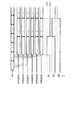
したがって、図6に示されるように、クロック信号CLXおよび反転クロック信号CL
Xinvのデューティ比が50%であって、当該クロック信号CLXの1周期分のパルス幅
を有するスタートパルスDXが、クロック信号CLXの立ち下がり時にて1段目の単位回
路144に供給されると、出力信号n1は、スタートパルスDXをクロック信号CLXの
半周期だけ遅延した波形となり、以下、出力信号n2、n3、n4、…、n320は、出力信号
n1からクロック信号CLXの論理レベルが反転する毎に、すなわち、クロック信号CL
Xの半周期(B)毎に、順番に遅延した関係となる。
このため、各段の単位回路144において入力信号と出力信号との論理積信号であるサ
ンプリング信号S1、S2、S3、S4、…、S320は、同図に示されるように、クロック信
号CLXの半周期毎に、排他的に順番でHレベルとなるパルス信号となる。
Therefore, as shown in FIG. 6, the clock signal CLX and the inverted clock signal CL
When a start pulse DX having a duty ratio of Xinv of 50% and having a pulse width corresponding to one cycle of the clock signal CLX is supplied to the
The relationship is delayed in order for every half cycle (B) of X.
Therefore, the sampling signals S1, S2, S3, S4,..., S320, which are logical products of the input signal and the output signal in the
図6では、サンプリング信号S1、S2、S3、S4、…、S320が順番にHレベルとなる
期間を水平走査有効期間(Ha)と表記する。制御回路210は、水平走査期間(H)が
水平走査有効期間(Ha)を含むように走査線駆動回路130を制御する。また、図6で
は、水平走査期間(H)のうち、水平走査有効期間(Fa)以外を水平走査帰線期間(Hb
)として表記している。
In FIG. 6, a period in which the sampling signals S1, S2, S3, S4,..., S320 are sequentially at the H level is denoted as a horizontal scanning effective period (Ha). The
).
6本の画像信号線170は、ブロック選択回路142とサンプリング回路146との間
において、X方向に沿って互いに平行となるように配列している。データ線114は、Y
方向に沿った方向に設けられているので、画像信号線170は、データ線114を仮想的
に延長した線上と交差することになる。
一方、6本の接続信号線172は、6本の画像信号線170と一対一に対応して設けら
れ、素子基板の接続端子174から、1段目の単位回路144と2段目の単位回路144
との間を結ぶ連絡信号線181と交差するように設けられている。ここで、6本の接続信
号線172のうち、図2において最左端のものは、6本の画像信号線170の最下端に位
置するものに接続され、同様に左から数えて2、3、4、5、6番目の接続信号線172
は、下から数えて2、3、4、5、6番目の画像信号線170にそれぞれ接続されている
。
ここで、6本の接続信号線172には、左から数えて順番にデータ信号R1、G1、B1
、R2、G2、B2が、それぞれ処理回路20から供給される。このため、6本の画像信号
線170にも、下から数えて順番にデータ信号R1、G1、B1、R2、G2、B2が、それぞ
れ供給されることになる。
したがって、本実施形態において6本の画像信号線170に供給されるデータ信号の色
と一ブロックにおける6列のデータ線114が対応する画素の色との配列は、縦方向と横
方向との相違はあるが、配列方向でみたときにはRGBRGBで同一となる。
The six
Since the
On the other hand, the six
Are provided so as to intersect with a
Are connected to the second, third, fourth, fifth and sixth
Here, the six
, R2, G2, and B2 are supplied from the
Therefore, in this embodiment, the arrangement of the color of the data signal supplied to the six
サンプリング回路146は、1〜1920列のデータ線114の各々に設けられたTF
T148から構成される。TFT148は、サンプリングスイッチとして機能するもので
あり、そのドレイン電極148は、データ線114の一端に接続されている。
ここで、TFT148のソース電極は、6本の画像信号線170のいずれかに、次のよ
うな関係で接続される。すなわち、データ線114を一般化して説明するために、1≦j
≦1920を満たす整数のjを用いると、図2において左から数えてj列目のデータ線1
14に対応するTFT148のソース電極は、列数であるjを6で割った余りが「1」で
あるならば、データ信号R1が供給される画像信号線170に接続され、jを6で割った
余りが「2」、「3」、「4」、「5」、「0」であるデータ線114に対応するTFT
148のソース電極は、それぞれデータ信号G1、B1、R2、G2、B2が供給される画像
信号線170に接続される。例えば、左から数えて9列目のデータ線114に対応するT
FT148のソース電極は、「9」を6で割った余りが「3」であるから、データ信号B
1が供給される画像信号線170に接続される。
The
It is composed of T148. The
Here, the source electrode of the
When an integer j satisfying ≦ 1920 is used, the
The source electrode of the
The
The source electrode of the
1 is connected to the supplied
また、TFT148のゲート電極は、同一ブロックに対応するもの同士で共通接続され
て、ブロックに対応した単位回路144のサンプリング信号が供給される。例えば、7列
目から12列目までの6列のデータ線114に対応するTFT148のゲート電極には、
当該6列のデータ線114が2番目のブロックに対応していることから、サンプリング信
号S2が共通に供給される。
ここで、あるブロックに対応したサンプリング信号がHレベルになると、当該ブロック
に属する6個のTFT148がソース・ドレイン電極間で導通状態となるので、6本の画
像信号線170に供給されたデータ信号が、それぞれ当該ブロックに属する6列のデータ
線114にサンプリングされることになる。
The gate electrodes of the
Since the six columns of
Here, when the sampling signal corresponding to a certain block becomes H level, the six
次に、本実施形態に係る電気光学装置の動作について説明する。
まず、画像データVdは、ドットでみたときに1行1列〜1行640列、2行1列〜2
行640列、3行1列〜3行640列、…、480行1列〜480行640列、という順
番で上位装置から供給される。この画像データVdは、ドットクロックDclkに同期してド
ット毎に供給され、S/P変換回路220によって図7に示されるように画像データVd1
d〜Vd6dに相展開処理される。
図7は、ある1行のドットに対応する画像データVdのS/P変換処理を示している。
詳細には、奇数列のドットに対応した画像データVdが、それぞれR、G、Bの階調を指
定する画像データVd1d〜Vd3dに遅延分配されて、時間軸に2倍に伸長され、この伸長さ
れた期間と一致するように、当該奇数列に続く偶数列のドットに対応した画像データVd
が、それぞれR、G、Bの階調を指定する画像データVd4d〜Vd6dに分配されて、時間軸
に2倍に伸長される相展開処理される様子を示している。
Next, the operation of the electro-optical device according to this embodiment will be described.
First, when the image data Vd is viewed as dots, it is 1
340 rows, 3 rows and 1 column to 3 rows and 640 columns,... 480 rows and 1 column to 480 rows and 640 columns are supplied from the host device. This image data Vd is supplied for each dot in synchronization with the dot clock Dclk, and the image data Vd1 is displayed by the S /
Phase expansion processing is performed from d to Vd6d.
FIG. 7 shows the S / P conversion processing of the image data Vd corresponding to a certain line of dots.
Specifically, the image data Vd corresponding to the odd-numbered dots is delayed and distributed to the image data Vd1d to Vd3d designating the gradations of R, G, and B, respectively, and is expanded twice as much as the time axis. Image data Vd corresponding to the dots in the even-numbered columns following the odd-numbered columns so as to coincide with the recorded period
Shows a state in which the phase expansion processing is performed, which is distributed to the image data Vd4d to Vd6d specifying the gradations of R, G, and B, respectively, and is expanded twice on the time axis.
なお、制御回路210は、1、2列目のドットに対応する画像データVd1d〜Vd6dが出
力される期間にサンプリングS1がHレベルとなり、続く3、4列目のドットに対応する
画像データVd1d〜Vd6dが出力される期間にサンプリングS2がHレベルとなり、以下同
様に、奇数列および当該奇数列に続く偶数列のドットに対応した画像データVdが相展開
処理される毎に順番にサンプリング信号がHレベルとなるように、スタートパルスDXお
よびクロック信号CLX(反転クロック信号CLXinvを出力する)。
詳細には、クロック信号CLXの立ち下がり時にクロック信号CLXの1周期分のパル
ス幅を有するスタートパルスDXを供給してから、クロック信号CLXの半周期後に、サ
ンプリング信号S1がHレベルとなり、以下順次、クロック信号CLXの半周期ずつ遅延
してサンプリング信号S2、S3、S4、…、S320がHレベルとなるので、制御回路210
は、1、2列目のドットに対応する画像データVd1d〜Vd6dが出力されるタイミングより
もクロック信号CLXの半周期分だけ先んじたタイミングでスタートパルスDXをHレベ
ルとさせるとともに、S/P変換回路220において奇数列および当該奇数列に続く偶数
列のドットに対応した画像データVdを相展開処理する毎にクロック信号CLX(反転ク
ロック信号inv)を論理反転して出力する。
In the
Specifically, the sampling signal S1 becomes H level after a half cycle of the clock signal CLX after supplying the start pulse DX having a pulse width corresponding to one cycle of the clock signal CLX when the clock signal CLX falls. The sampling signals S2, S3, S4,..., S320 are delayed by half a cycle of the clock signal CLX, so that the
Causes the start pulse DX to be at the H level at a timing that precedes the timing at which the image data Vd1d to Vd6d corresponding to the dots in the first and second columns are output by a half cycle of the clock signal CLX, and S / P conversion. The clock signal CLX (inverted clock signal inv) is logically inverted and output every time the image data Vd corresponding to the odd-numbered column and the even-numbered dot following the odd-numbered column is subjected to the phase expansion processing in the
上述したように液晶素子120に対するデータ信号は正極性と負極性とで指定されるが
、本実施形態では、1行毎に書込極性を反転させる行反転(ライン反転ともいう)とし、
さらに、同一行について垂直走査期間(F)毎に正極性と負極性とで交互に反転させる駆
動として説明する。なお、ここでは、垂直走査期間の奇数行で正極性書込を指定するもの
とする。
この垂直走査期間において、まず1行目の走査線112が選択されて、走査信号Y1が
Hレベルになる。走査信号Y1がHレベルになると、1行目に位置する画素110、すな
わち、1行1列〜1行1920列のTFT116がオンする。
また、制御回路210は、1行1列および1行2列のドットの画像データVdを相展開
処理して、この相展開処理に合わせてサンプリング信号S1がHレベルとなるように、上
述したようにスタートパルスDX、クロック信号CLX(反転クロック信号CLXinv)
を出力する。
ここで、サンプリング信号S1がHレベルとなるとき、接続信号線172を介して画像
信号線170に供給されるデータ信号R1は、1行1列のドットにおけるRの画像データ
Vd1dを正極性に変換した信号である。画像信号線170に供給されるデータ信号G1、B
1は、1行1列のドットにおけるGの画像データVd2d、Bの画像データVd3dを、それぞ
れ正極性に変換した信号であり、同様に、画像信号線170に供給されるデータ信号R2
、G2、B2は、1行2列のドットにおけるRの画像データVd4d、Gの画像データVd5d、
Bの画像データVd6dを、それぞれ正極性に変換した信号である。
As described above, the data signal for the
Further, a description will be given of driving in which the same row is alternately inverted between positive polarity and negative polarity for each vertical scanning period (F). Here, it is assumed that positive polarity writing is designated in odd rows in the vertical scanning period.
In this vertical scanning period, first, the
Further, the
Is output.
Here, when the sampling signal S1 becomes H level, the data signal R1 supplied to the
1 is a signal obtained by converting the G image data Vd2d and the B image data Vd3d in the dot of 1 row and 1 column to positive polarity, respectively, and similarly, the data signal R2 supplied to the
, G2, B2 are R image data Vd4d, G image data Vd5d, and G image data Vd5d for dots in one row and two columns.
This is a signal obtained by converting the B image data Vd6d to positive polarity.
サンプリング信号S1がHレベルになると、第1番目のブロックに属する1〜6列目の
TFT148がオンする。このため、6本画像信号線170に供給されたデータ信号R1
、G1、B1、R2、G2、B2が、1〜6列目のそれぞれに対応するデータ線114にサン
プリングされるので、1行1列〜1行6列の画素電極118には、オン状態にあるTFT
116を介して、それぞれの色の階調に応じた正極性電圧が印加されることになる。
When the sampling signal S1 becomes H level, the
, G1, B1, R2, G2, and B2 are sampled on the
A positive voltage corresponding to the gradation of each color is applied via 116.
次に、サンプリング信号S2がHレベルとなる。サンプリング信号S2がHレベルとなる
とき、接続信号線172を介して画像信号線170に供給されるデータ信号R1、G1、B
1は、1行3列のドットにおけるRの画像データVd1d、Gの画像データVd2d、Bの画像
データVd3dを、それぞれ正極性に変換した信号であり、同様に、データ信号R2、G2、
B2は、1行4列のドットにおけるRの画像データVd4d、Gの画像データVd5d、Bの画
像データVd6dを、それぞれ正極性に変換した信号である。
サンプリング信号S2がHレベルになると、第2番目のブロックに属する7〜12列目
のTFT148がオンするので、6本画像信号線170に供給されたデータ信号R1、G1
、B1、R2、G2、B2が、7〜12列目のそれぞれに対応するデータ線114にサンプリ
ングされる。このため、1行7列〜1行12列の画素電極118には、オン状態にあるT
FT116を介して、それぞれの色の階調に応じた正極性電圧が印加されることになる。
Next, the sampling signal S2 becomes H level. When the sampling signal S2 becomes H level, the data signals R1, G1, B supplied to the
1 is a signal obtained by converting the R image data Vd1d, the G image data Vd2d, and the B image data Vd3d in the dot of 1 row and 3 columns into positive polarity, respectively. Similarly, the data signals R2, G2,
B2 is a signal obtained by converting the R image data Vd4d, the G image data Vd5d, and the B image data Vd6d into dots of 1 row and 4 columns, respectively, to positive polarity.
When the sampling signal S2 becomes H level, the
, B1, R2, G2, and B2 are sampled on the
A positive voltage corresponding to the gradation of each color is applied via the
以下同様な動作が、サンプリング信号S320がHレベルとなるまで繰り返され、これに
より、1行1列から1行1920列の画素電極118には、それぞれの色の階調に応じた
正極性電圧が印加されることになる。その後、水平走査帰線期間(Hb)を経て、2行目
の走査線112が選択され、走査信号Y2がHレベルになる。なお、走査信号Y2がHレベ
ルになると、走査信号Y1がLレベルになるので、1行1列〜1行1920列のTFT1
16がオフするが、オン時に画素電極118に印加された電圧は、液晶素子120の容量
性によって保持される。
また、2行目の走査線112が選択されたとき、1行目の走査線112の選択時と同様
に、2行1列〜2行1920列のTFT116がオンし、サンプリング信号S1、S2、S
3、S4、…、S320が順番にHレベルになるが、データ信号R1、G1、B1、R2、G2、B
2の極性は反転されて負極性となるので、2行1列〜2行1920列の画素電極118に
は、それぞれの色の階調に応じた負極性電圧が印加される。
以下同様な動作が、3、4、5、6、…、480行目で繰り返される。これにより、奇
数行の画素電極118には、それぞれの色の階調に応じた正極性電圧が印加され、偶数行
の画素電極118には、それぞれの色の階調に応じた負極性電圧が印加される。
次の垂直走査期間でも同様な動作が繰り返されるが、極性が反転されるので、奇数行の
画素電極118には、それぞれの色の階調に応じた負極性電圧が印加され、偶数行の画素
電極118には、それぞれの色の階調に応じた正極性電圧が印加される。
Thereafter, the same operation is repeated until the sampling signal S320 becomes H level, whereby a positive voltage corresponding to the gradation of each color is applied to the
16 is turned off, but the voltage applied to the
When the
3, S4,..., S320 sequentially become H level, but the data signals R1, G1, B1, R2, G2, B
Since the polarity of 2 is inverted to become negative, a negative voltage corresponding to the gradation of each color is applied to the
Thereafter, the same operation is repeated in the third, fourth, fifth, sixth,. As a result, a positive voltage corresponding to the gradation of each color is applied to the
The same operation is repeated in the next vertical scanning period. However, since the polarity is inverted, the negative polarity voltage corresponding to the gradation of each color is applied to the
図8は、i行目およびこれに隣接する(i+1)行目の走査線112が選択される水平
走査期間(H)のそれぞれにおいて、例えばデータ信号R1のの電圧波形の一例を示す図
である。
この図において、電圧Vb(+)、Vb(-)は、それぞれ最低階調の黒色に相当する正極性、
負極性電圧であり、基準電圧Vcを中心に対称の関係にある。
ここで、画像データVdがR、G、Bの各色の階調値をそれぞれ例えば8ビットで指定
するとともに、当該階調値が十進値表記で「0」のときに最も暗い階調を指定し、以後当
該十進値が大きくなるにつれて徐々に明るい階調を指定し、十進値表記で「255」のと
きに最も明るい階調を指定する場合、本実施形態ではノーマリーブラックモードを想定し
ているので、データ信号R1の電圧は、正極性に変換する場合であれば、階調値が大きく
なるにつれて電圧Vb(+)から高位側に振った電圧となり、負極性に変換する場合であれば
、電圧Vb(-)から低位側に振った電圧となる。
FIG. 8 is a diagram illustrating an example of a voltage waveform of the data signal R1, for example, in each of the horizontal scanning period (H) in which the i-th row and the (i + 1) -
In this figure, the voltages Vb (+) and Vb (−) are positive polarity corresponding to the black of the lowest gradation,
It is a negative voltage and has a symmetrical relationship with respect to the reference voltage Vc.
Here, the gradation value of each color of R, G, B is designated by, for example, 8 bits in the image data Vd, and the darkest gradation is designated when the gradation value is “0” in decimal notation. In the present embodiment, normally black mode is assumed when the lighter gradation is specified gradually as the decimal value increases, and the brightest gradation is specified when the decimal value is “255”. Therefore, if the voltage of the data signal R1 is converted to the positive polarity, the voltage swings from the voltage Vb (+) to the higher side as the gradation value increases, and converted to the negative polarity. If so, the voltage is shifted from the voltage Vb (−) to the lower side.
なお、コモン電極108に印加される電圧LCcomは、図8に示されるように、基準電
圧Vcよりも低位側に設定される。これは、nチャネル型のTFT116では、ゲート・
ドレイン電極間の寄生容量に起因して、オンからオフに状態変化するときにドレイン(画
素電極118)の電位が低下する、というプッシュダウンが発生するためである。仮に電
圧LCcomを基準電圧Vcと一致させた場合、負極性書込による液晶素子120の電圧実効
値が、プッシュダウンのために、正極性書込による電圧実効値よりも若干大きくなってし
まう(TFT116がnチャネルの場合)。このため、プッシュダウンの影響が相殺され
るように、電圧LCcomを基準電圧Vcよりも低位側にオフセットして設定しているのであ
る。ただし、プッシュダウンの影響が無視できるならば、電圧LCcomと基準電圧Vcとを
一致させても良い。
Note that the voltage LCcom applied to the
This is because, due to the parasitic capacitance between the drain electrodes, a push-down occurs in which the potential of the drain (pixel electrode 118) decreases when the state changes from on to off. If the voltage LCcom is matched with the reference voltage Vc, the effective voltage value of the
i行目の液晶素子120に正極性が指定された場合、走査信号YiがHレベルになる水
平走査期間(H)においてサンプリング信号S1がHレベルになるとき、データ信号R1は
、i行1列のR画素の階調に応じた正極性電圧となり、以降、サンプリング信号の変化に
合わせて、7、13、19、…、1915列目のR画素の階調に応じた正極性電圧に変化
する。
続いて選択される(i+1)行目では、極性が反転して負極性が指定されるので、走査
信号Y(i+1)がHレベルになる水平走査期間(H)において、サンプリング信号S1がHレ
ベルになるとき、データ信号R1は、(i+1)行1列のR画素の階調に応じた負極性電
圧となり、以降、サンプリング信号の変化に合わせて、7、13、19、…、1915列
目のR画素の階調に応じた負極性電圧に変化する。
なお、図8においてデータ信号R1の電圧を示す縦スケールは、便宜的に他の信号にお
ける縦スケールよりも拡大してある。また、サンプリング信号S320がLレベルに変化し
てからサンプリング信号S1がHレベルに変化するまでの水平走査帰線期間(Hb)にわた
って黒色に相当する電圧となっているが、その理由は、タイミングずれなどの理由により
誤って画素に書き込まれても、表示に寄与させないためである。
また、図8においては、データ信号R1の電圧波形を一例として示したが、他のデータ
信号G1、B1、R2、G2、B2についても階調に応じた電圧に変換される。
When positive polarity is specified for the
In the subsequently selected row (i + 1), since the polarity is inverted and the negative polarity is designated, the sampling signal S1 is in the horizontal scanning period (H) in which the scanning signal Y (i + 1) is at the H level. When the signal level becomes H level, the data signal R1 becomes a negative voltage corresponding to the gradation of the R pixel in (i + 1) rows and 1 column, and thereafter, 7, 13, 19,..., 1915 in accordance with the change of the sampling signal. It changes to a negative voltage corresponding to the gradation of the R pixel in the column.
In FIG. 8, the vertical scale indicating the voltage of the data signal R1 is enlarged for convenience in comparison with the vertical scales of other signals. Further, the voltage corresponds to black over the horizontal scanning blanking period (Hb) from when the sampling signal S320 changes to the L level to when the sampling signal S1 changes to the H level. This is because even if the data is erroneously written to the pixel for reasons such as the above, it does not contribute to display.
In FIG. 8, the voltage waveform of the data signal R1 is shown as an example, but the other data signals G1, B1, R2, G2, and B2 are also converted to voltages according to the gradation.
本実施形態では、6本の画像信号線170は、それぞれ1段目および2段目の単位回路
144の間を通過する6本の接続信号線172を介して接続される。ここで、6本の画像
信号線170が、素子基板のX方向に沿った辺に設けられた接続端子174にそれぞれ直
接接続される従来構成では、図14に示されるように、画像信号線170をブロック選択
回路142に回り込むように配線する必要がある。
このため、同図において画像信号線170が廻り込む部分Xa、Xbだけ余計に基板スペ
ースが必要となり、基板の縮小による低コスト化や、額縁の狭小化による実装自由度の向
上などを阻害する要因となった。特にここではS/P変換における相展開数を「6」とし
て説明しているが、「12」、「24」、…、「96」というように相展開数が増大する
につれて、部分Xa、Xbが大きくなり、基板スペースを広く必要となるので、無視できな
い問題となる。
これに対して本実施形態では、画像信号線170が廻り込む替わりに、単位回路144
の間を通過する接続信号線172を介して、接続端子174にそれぞれ接続させた構成と
しているので、部分Xa、Xbのスペースが不要となり、基板の縮小化や、額縁の狭小化が
可能となる。
In the present embodiment, the six
For this reason, in the same figure, an extra board space is required only for the portions Xa and Xb where the
On the other hand, in the present embodiment, instead of the
Since the
ところで、本実施形態のように、接続信号線172を、接続端子174から単位回路1
44の間を通過させて画像信号線170まで引き回すと、当該接続信号線172は、1段
目の単位回路144の出力端と次段である2段目の単位回路144の入力端とを結ぶ連絡
信号線181と、クロック信号CLXを供給する信号線と、反転クロック信号CLXinv
を供給する信号線と、それぞれ交差する。このため、一見すると、これらの信号線による
ノイズが、接続信号線172に供給されるアナログのデータ信号R1、G1、B1、R2、G
2、B2に伝搬し、データ線114にサンプリングされる電圧を変動させて、表示に悪影響
を与えるようにも見える。
しかしながら、クロック信号CLXの論理信号を反転させたものが反転クロック信号C
LXinvであるので、図9に示されるように、クロック信号CLXの論理レベルが変化し
たときに現れるノイズと、反転クロック信号CLXinvの論理レベルが変化したときに現
れるノイズとは、互いに逆向きであって同じ大きさであるので、相殺し合う。このため、
本実施形態では、接続信号線172において、クロック信号CLXを供給する信号線と、
反転クロック信号CLXinvを供給する信号線とそれぞれ交差することによるノイズの影
響は、ほとんど無視できると考えられる。
さらに、連絡信号線181に供給される信号は、本実施形態では、1段目の単位回路1
44による出力信号n1であり、水平走査期間(H)において1回の割合でL→H→Lレ
ベルと変化するのみである。このため、接続信号線172において、連絡信号線181と
交差することによるノイズの影響についても、ほとんど無視できると考えられる。
By the way, as in the present embodiment, the
44, the
Crosses each of the signal lines for supplying. Therefore, at first glance, noise due to these signal lines may cause analog data signals R1, G1, B1, R2, G, which are supplied to the
2, it also propagates to B2 and fluctuates the voltage sampled on the
However, an inverted version of the logic signal of the clock signal CLX is the inverted clock signal C.
Since it is LXinv, as shown in FIG. 9, the noise that appears when the logic level of the clock signal CLX changes and the noise that appears when the logic level of the inverted clock signal CLXinv change are opposite to each other. Because they are the same size, they cancel each other. For this reason,
In the present embodiment, in the
It can be considered that the influence of noise caused by crossing each of the signal lines supplying the inverted clock signal CLXinv is almost negligible.
Further, in the present embodiment, the signal supplied to the
44 is an output signal n1 and only changes from L → H → L level at a rate of once in the horizontal scanning period (H). For this reason, it is considered that the influence of noise caused by the
本実施形態では、表示パネル10と処理回路20とをFPC基板で接続する構成とした
が、図10に示されるように、処理回路20の一部または全部の機能を実行するICチッ
プを、素子基板の領域190においてCOG(chip on glass)等の技術を用いて実装し
ても良い。
また、本実施形態では、接続信号線172を1段目および2段目の単位回路144の間
を通過させたが、画像信号線170に供給されるデータ信号の遅延が左右端で異なってし
まうことが問題となるのであれば、接続信号線172を、例えば160段目と161段目
の単位回路144の間を通過させて画像信号線170のほぼ中心に接続する構成が望まし
い。
In the present embodiment, the
In the present embodiment, the
次に、本発明の第2実施形態に係る電気光学装置について説明する。この第2実施形態
では、表示パネル10における接続信号線172を第1実施形態から変更したものである
。なお、それ以外については第1実施形態と共通であるので、説明を省略する。
Next, an electro-optical device according to a second embodiment of the invention will be described. In the second embodiment, the
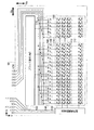
図11は、第2実施形態における表示パネル10の構成を示す平面図である。
この図に示されるように第2実施形態では、接続信号線172をR、G、Bの色毎に分
類し、同じ色の接続信号線172については、接続端子174から同じ単位回路144の
間を通過させて画像信号線170に接続する構成となっている。
詳細には、本実施形態において1ブロックを構成するデータ線数は「6」であるので、
Rの接続信号線172の2本が1段目および2段目の単位回路144の間を結ぶ連絡信号
線181と交差するように設けられ、Gの接続信号線172の2本が2段目および3段目
の単位回路144の間を結ぶ連絡信号線182と交差するように設けられ、Bの接続信号
線172の2本が3段目および4段目の単位回路144の間を結ぶ連絡信号線183と交
差するように設けられた構成となっている。
FIG. 11 is a plan view showing the configuration of the
As shown in this figure, in the second embodiment, the
Specifically, in this embodiment, the number of data lines constituting one block is “6”.
Two of the R
このような第2実施形態によれば、基板スペースの縮小化や、額縁の狭小化が可能とな
るほか、同じ色の接続信号線172についてみたときの時定数が第1実施形態と比較して
近接するので、画像信号線170に供給されるデータ信号の電圧が接続信号線172同士
の時定数のばらつきにより不均等になることが防止される。このため、列方向に現れる表
示ムラの発生を抑えることが可能となる。
なお、この第2実施形態では、複数の色同士を、例えばR、Gの接続信号線172の4
本を、同じ単位回路144の間を通過させ、Bの接続信号線172の2本を、他の単位回
路144の間を通過させる構成としても良い。
According to the second embodiment, the board space can be reduced and the frame can be narrowed, and the time constant when the
In the second embodiment, a plurality of colors are connected to, for example, 4 of R and G connection signal lines 172.
The book may pass between the
次に、本発明の第3実施形態に係る電気光学装置について説明する。この第3実施形態
では、表示パネル10における接続信号線172、および、画像信号線170の順序を第
1実施形態から変更したものである。なお、それ以外については第1実施形態と共通であ
るので、説明を省略する。
Next, an electro-optical device according to a third embodiment of the invention will be described. In the third embodiment, the order of the
図12は、第3実施形態における表示パネル10の構成を示す平面図である。
この図に示されるように第3実施形態では、接続信号線172をR、G、Bの色毎に分
類し、同じ色の接続信号線172については、接続端子174から同じ単位回路144の
間を通過させて画像信号線170に接続する構成とした点までは、第2実施形態と同様で
あるが、画像信号線170に供給されるデータ信号が、下から順番に、R1、R2、G1、
G2、B1、B2となって、同色で2本ずつまとめられて点において第2実施形態と相違し
ている。
このような第3実施形態によれば、基板スペースの縮小化や、額縁の狭小化が可能とな
るほか、同じ色の接続信号線172のみならず、画像信号線170についてみたときの時
定数が近接するので、列方向に現れる表示ムラの発生をより効果的に抑えることが可能と
なる。
FIG. 12 is a plan view showing the configuration of the
As shown in this figure, in the third embodiment, the
G2, B1, and B2 are different from the second embodiment in that they are grouped by two in the same color.
According to the third embodiment, the board space can be reduced and the frame can be narrowed. In addition to the
なお、上述した各実施形態では、S/P変換回路220における相展開数を「6」とし
たが、「9」、「12」、「15」、…、というように増加させても良いし、相展開しな
い「3」としても良い。また、R、G、Bの3色で1ドットを表現したが、さらにEg(
エメラルドグリーン)などの色を追加して4色以上で1ドットを表現しても良い。
ここで、相展開数のmは、1ドットを表現するための色数を3以上のnとしたときに、
n倍数であれば良い。
In each of the embodiments described above, the number of phase expansions in the S /
Colors such as emerald green) may be added to express one dot with four or more colors.
Here, the number m of phase expansions is n when the number of colors for expressing one dot is 3 or more.
Any multiple of n is sufficient.
また、各実施形態では、ブロック選択回路142がスタートパルスDXを図2において
右方向のみに転送する構成として説明したが、転送方向制御信号DIRなどを用いて左右
の双方向のいずれにも転送可能とする構成としても良い。
さらに、実施形態では、液晶素子120について、ノーマリーブラックモードとして説
明したが、電圧無印加状態で白色表示となるノーマリーホワイトモードとしても良いし、
透過型に限られず、反射型や、両者の中間的な半透過半反射型であっても良い。
くわえて、画像信号線170にアナログのデータ信号が供給される構成のすべてに適用
可能である。このため、画素としては、液晶素子を用いたものに限られず、例えば、EL
(Electronic Luminescence)素子、電子放出素子、電気泳動素子などを用いたものにも
適用可能である。
In each of the embodiments, the
Furthermore, in the embodiment, the
It is not limited to the transmissive type, and may be a reflective type or a semi-transmissive / semi-reflective type intermediate between the two.
In addition, the present invention can be applied to all configurations in which an analog data signal is supplied to the
(Electronic Luminescence) It is applicable also to the thing using an electron emission element, an electrophoretic element, etc.
<電子機器>
次に、上述した実施形態に係る電気光学装置1を表示装置として有する電子機器の例に
ついて説明する。
図13は、実施形態に係る電気光学装置1を用いた携帯電話1200の構成を示す図で
ある。この図に示されるように、携帯電話1200は、複数の操作ボタン1202のほか
、受話口1204、送話口1206とともに、上述した電気光学装置1を備える。
なお、電気光学装置1が適用される電子機器としては、図13に示した携帯電話の他に
も、デジタルスチルカメラ、ノートパソコン、液晶テレビ、ビデオレコーダ、カーナビゲ
ーション装置、ページャ、電子手帳、電卓、ワードプロセッサ、ワークステーション、テ
レビ電話、POS端末、タッチパネル等などの機器が挙げられる。そして、これらの各種
電子機器の表示装置として、上述した電気光学装置1が適用可能であることは言うまでも
ない。
<Electronic equipment>
Next, an example of an electronic apparatus having the electro-
FIG. 13 is a diagram illustrating a configuration of a
As an electronic apparatus to which the electro-
1…電気光学装置、10…表示パネル、20…処理回路、100…表示領域、108…コ
モン電極、112…走査線、114…データ線、116…TFT、118…画素電極、1
20…液晶素子、130…走査線駆動回路、142…ブロック選択回路、142…単位回
路、146…サンプリング回路、170…画像信号線、172…接続信号線、181…連
絡信号線、1200…携帯電話機
DESCRIPTION OF
DESCRIPTION OF
Claims (5)
複数m本の画像信号線と、
前記m本の画像信号線の各々と対をなすように設けられ、各々は、それぞれ対をなす画像信号線に接続されて、データ信号を供給するm本の接続信号線と、
m本毎にブロック化されたデータ線であって、一つのブロックにおけるm本のデータ線は、前記m本の画像信号線のそれぞれと対をなすように設けられた複数のデータ線と、
前記複数の走査線を所定の順番で選択する走査線駆動回路と、
一本の走査線に選択される期間にわたって、前記ブロックの選択を示すサンプリング信号を所定の順番で出力するブロック選択回路と、
前記複数のデータ線のそれぞれに設けられ、各々は、前記サンプリング信号がブロックの選択を示すときに、対をなす画像信号線とデータ線との間でオン状態となるサンプリングスイッチと、
前記複数の走査線と前記複数のデータ線との交差に対応して設けられ、各々は、前記走査線が選択されたときに、前記データ線にサンプリングされたデータ信号に応じた階調となる画素と、
を備え、
前記ブロック選択回路は、出力端が次段の入力端に接続された単位回路を複数個有し、
前記複数個の単位回路の各々は、前記入力端に供給されたパルスを所定時間遅延させて出力端から出力するとともに、入力端および出力端に供給されたパルスに基づいてサンプリング信号を出力し、
前記接続信号線は、一の単位回路の出力端と次段の単位回路の入力端との間を結ぶ連絡信号線と交差するように設けられ、
前記画素は、n(nは3以上の整数)色のうち、いずれかであり、
前記mはnの倍数であり、
一つのブロックに属するm本のデータ線は、前記n色の画素に対応するものが所定の順番で繰り返して配列し、
前記m本の画像信号線は、前記m本のデータ線における色と同じ順番で繰り返して配列し、
同色に対応する画像信号線に接続されたm/n本の接続信号線が、少なくとも同一の連絡信号線と交差するように設けられている
ことを特徴とする電気光学装置。 A plurality of scan lines;
A plurality of m image signal lines;
A pair of m image signal lines, each of which is connected to a pair of image signal lines and supplying a data signal;
a plurality of data lines, each of which is divided into m data lines, wherein the m data lines in one block are paired with each of the m image signal lines;
A scanning line driving circuit for selecting the plurality of scanning lines in a predetermined order;
A block selection circuit that outputs a sampling signal indicating selection of the block in a predetermined order over a period selected by one scanning line;
A sampling switch provided in each of the plurality of data lines, each of which is turned on between a pair of image signal lines and data lines when the sampling signal indicates selection of a block;
Provided corresponding to the intersection of the plurality of scanning lines and the plurality of data lines, each having a gradation corresponding to a data signal sampled on the data line when the scanning line is selected. Pixels,
With
The block selection circuit has a plurality of unit circuits whose output terminals are connected to the input terminals of the next stage,
Each of the plurality of unit circuits delays the pulse supplied to the input terminal for a predetermined time and outputs it from the output terminal, and outputs a sampling signal based on the pulses supplied to the input terminal and the output terminal,
The connection signal line is provided so as to intersect with a connection signal line connecting between an output end of one unit circuit and an input end of a unit circuit of the next stage,
The pixel is one of n (n is an integer of 3 or more) colors,
M is a multiple of n;
M data lines belonging to one block are repeatedly arranged in a predetermined order corresponding to the n color pixels,
The m image signal lines are repeatedly arranged in the same order as the colors of the m data lines,
An electro-optical device, wherein m / n connection signal lines connected to image signal lines corresponding to the same color are provided so as to intersect at least the same communication signal line .
複数m本の画像信号線と、 A plurality of m image signal lines;
前記m本の画像信号線の各々と対をなすように設けられ、各々は、それぞれ対をなす画像信号線に接続されて、データ信号を供給するm本の接続信号線と、 A pair of m image signal lines, each of which is connected to a pair of image signal lines and supplying a data signal;
m本毎にブロック化されたデータ線であって、一つのブロックにおけるm本のデータ線は、前記m本の画像信号線のそれぞれと対をなすように設けられた複数のデータ線と、 a plurality of data lines, each of which is divided into m data lines, wherein the m data lines in one block are paired with each of the m image signal lines;
前記複数の走査線を所定の順番で選択する走査線駆動回路と、 A scanning line driving circuit for selecting the plurality of scanning lines in a predetermined order;
一本の走査線に選択される期間にわたって、前記ブロックの選択を示すサンプリング信号を所定の順番で出力するブロック選択回路と、 A block selection circuit that outputs a sampling signal indicating selection of the block in a predetermined order over a period selected by one scanning line;
前記複数のデータ線のそれぞれに設けられ、各々は、前記サンプリング信号がブロックの選択を示すときに、対をなす画像信号線とデータ線との間でオン状態となるサンプリングスイッチと、 A sampling switch provided in each of the plurality of data lines, each of which is turned on between a pair of image signal lines and data lines when the sampling signal indicates selection of a block;
前記複数の走査線と前記複数のデータ線との交差に対応して設けられ、各々は、前記走査線が選択されたときに、前記データ線にサンプリングされたデータ信号に応じた階調となる画素と、 Provided corresponding to the intersection of the plurality of scanning lines and the plurality of data lines, each having a gradation corresponding to a data signal sampled on the data line when the scanning line is selected. Pixels,
を備え、 With
前記ブロック選択回路は、出力端が次段の入力端に接続された単位回路を複数個有し、 The block selection circuit has a plurality of unit circuits whose output terminals are connected to the input terminals of the next stage,
前記複数個の単位回路の各々は、前記入力端に供給されたパルスを所定時間遅延させて出力端から出力するとともに、入力端および出力端に供給されたパルスに基づいてサンプリング信号を出力し、Each of the plurality of unit circuits delays the pulse supplied to the input terminal for a predetermined time and outputs it from the output terminal, and outputs a sampling signal based on the pulses supplied to the input terminal and the output terminal,
前記画素は、n(nは3以上の整数)色のうち、いずれかであり、 The pixel is one of n (n is an integer of 3 or more) colors,
前記mはnの倍数であり、 M is a multiple of n;
一つブロックに属するm本のデータ線は、前記n色の画素に対応するものが所定の順番で繰り返して配列し、 The m data lines belonging to one block are repeatedly arranged in a predetermined order corresponding to the n color pixels,
前記m本の画像信号線は、前記m/n本毎にまとまってデータ線の色と同じ順番で配列し、 The m image signal lines are arranged every m / n in the same order as the color of the data lines,
同色に対応する画像信号線に接続されたm/n本の接続信号線が、同一の連絡信号線と交差するように設けられている M / n connection signal lines connected to image signal lines corresponding to the same color are provided so as to intersect with the same communication signal line.
ことを特徴とする電気光学装置。 An electro-optical device.
前記単位回路の配列方向は、前記m本の画像信号線が設けられる方向に一致する
ことを特徴とする請求項1又は2に記載の電気光学装置。 The m image signal lines are provided in a direction intersecting with an extension line of the plurality of data lines,
The arrangement direction of the unit circuit, an electro-optical device according to claim 1 or 2, characterized in that matches the direction in which the image signal line of the m lines are provided.
Priority Applications (5)
| Application Number | Priority Date | Filing Date | Title |
|---|---|---|---|
| JP2007260619A JP4466710B2 (en) | 2007-10-04 | 2007-10-04 | Electro-optical device and electronic apparatus |
| US12/183,600 US8159431B2 (en) | 2007-10-04 | 2008-07-31 | Electrooptic device and electronic apparatus |
| CN2008101498199A CN101404146B (en) | 2007-10-04 | 2008-09-27 | Electrooptic device and electronic apparatus |
| KR1020080095932A KR100978168B1 (en) | 2007-10-04 | 2008-09-30 | Electrooptic device and electronic apparatus |
| TW097137865A TWI409741B (en) | 2007-10-04 | 2008-10-02 | Electrooptic device and electronic apparatus |
Applications Claiming Priority (1)
| Application Number | Priority Date | Filing Date | Title |
|---|---|---|---|
| JP2007260619A JP4466710B2 (en) | 2007-10-04 | 2007-10-04 | Electro-optical device and electronic apparatus |
Publications (2)
| Publication Number | Publication Date |
|---|---|
| JP2009092729A JP2009092729A (en) | 2009-04-30 |
| JP4466710B2 true JP4466710B2 (en) | 2010-05-26 |
Family
ID=40522840
Family Applications (1)
| Application Number | Title | Priority Date | Filing Date |
|---|---|---|---|
| JP2007260619A Expired - Fee Related JP4466710B2 (en) | 2007-10-04 | 2007-10-04 | Electro-optical device and electronic apparatus |
Country Status (5)
| Country | Link |
|---|---|
| US (1) | US8159431B2 (en) |
| JP (1) | JP4466710B2 (en) |
| KR (1) | KR100978168B1 (en) |
| CN (1) | CN101404146B (en) |
| TW (1) | TWI409741B (en) |
Families Citing this family (11)
| Publication number | Priority date | Publication date | Assignee | Title |
|---|---|---|---|---|
| TWI412012B (en) * | 2009-07-20 | 2013-10-11 | Au Optronics Corp | Liquid crystal display |
| JP5589469B2 (en) * | 2010-03-18 | 2014-09-17 | 株式会社リコー | Image forming apparatus and recording medium |
| KR101097351B1 (en) * | 2010-05-06 | 2011-12-23 | 삼성모바일디스플레이주식회사 | A scan driving circuit and a display apparatus using the same |
| TWI447692B (en) * | 2011-11-18 | 2014-08-01 | Au Optronics Corp | Display panel and multiplexer circuit therein, and method of transmitting signal in display panel |
| JP6005184B2 (en) * | 2013-01-18 | 2016-10-12 | シャープ株式会社 | Display device |
| TWI595296B (en) | 2014-09-23 | 2017-08-11 | 元太科技工業股份有限公司 | Display |
| JP6828247B2 (en) * | 2016-02-19 | 2021-02-10 | セイコーエプソン株式会社 | Display devices and electronic devices |
| CN108399900B (en) * | 2018-02-12 | 2022-11-22 | 厦门天马微电子有限公司 | Display device |
| CN108563082B (en) * | 2018-04-27 | 2020-12-22 | 京东方科技集团股份有限公司 | Circuit substrate, display device and driving method |
| JP7501062B2 (en) * | 2020-04-08 | 2024-06-18 | セイコーエプソン株式会社 | Electro-optical device and electronic device |
| CN111681591B (en) * | 2020-06-28 | 2022-12-13 | 厦门天马微电子有限公司 | Display module and display device |
Family Cites Families (24)
| Publication number | Priority date | Publication date | Assignee | Title |
|---|---|---|---|---|
| JP3734537B2 (en) * | 1995-09-19 | 2006-01-11 | シャープ株式会社 | Active matrix liquid crystal display device and driving method thereof |
| DE69820226T2 (en) * | 1997-10-31 | 2004-10-21 | Seiko Epson Corp | ELECTROOPTIC DEVICE AND ELECTRONIC DEVICE |
| US6300926B1 (en) * | 1998-04-27 | 2001-10-09 | Hitachi, Ltd. | Active matrix type liquid crystal display |
| JP2000171829A (en) | 1998-12-02 | 2000-06-23 | Sharp Corp | Semiconductor integrated circuit and picture display device |
| JP3428511B2 (en) * | 1999-07-02 | 2003-07-22 | 日本電気株式会社 | Active matrix type liquid crystal display |
| JP2001034237A (en) * | 1999-07-21 | 2001-02-09 | Fujitsu Ltd | Liquid crystal display device |
| JP4783890B2 (en) * | 2000-02-18 | 2011-09-28 | 株式会社 日立ディスプレイズ | Liquid crystal display |
| JP3596471B2 (en) * | 2000-03-27 | 2004-12-02 | セイコーエプソン株式会社 | Electro-optical device, method for manufacturing the same, and electronic apparatus |
| GB0014074D0 (en) * | 2000-06-10 | 2000-08-02 | Koninkl Philips Electronics Nv | Active matrix array devices |
| JP3498734B2 (en) * | 2000-08-28 | 2004-02-16 | セイコーエプソン株式会社 | Image processing circuit, image data processing method, electro-optical device, and electronic apparatus |
| JP2003022058A (en) * | 2001-07-09 | 2003-01-24 | Seiko Epson Corp | Electrooptic device, driving circuit for electrooptic device, driving method for electrooptic device, and electronic equipment |
| JP3729163B2 (en) * | 2001-08-23 | 2005-12-21 | セイコーエプソン株式会社 | Electro-optical panel driving circuit, driving method, electro-optical device, and electronic apparatus |
| JP4147872B2 (en) * | 2002-09-09 | 2008-09-10 | 日本電気株式会社 | Liquid crystal display device, driving method thereof, and liquid crystal projector device |
| CN1499473A (en) * | 2002-11-06 | 2004-05-26 | 统宝光电股份有限公司 | Liquid crystal display possessing configuration of circuit for driving data wire |
| JP2005024994A (en) * | 2003-07-04 | 2005-01-27 | Nidec Copal Corp | Lens back adjusting device |
| JP3846469B2 (en) * | 2003-10-01 | 2006-11-15 | セイコーエプソン株式会社 | Projection display device and liquid crystal panel |
| JP2005189758A (en) * | 2003-12-26 | 2005-07-14 | Sony Corp | Display device and projection display apparatus |
| US20050206597A1 (en) * | 2004-02-10 | 2005-09-22 | Seiko Epson Corporation | Electro-optical device, method for driving electro-optical device, driving circuit, and electronic apparatus |
| JP4529484B2 (en) | 2004-03-02 | 2010-08-25 | セイコーエプソン株式会社 | Electro-optical device and electronic apparatus |
| CN100449363C (en) * | 2004-06-18 | 2009-01-07 | 精工爱普生株式会社 | Electro-optical device and electronic apparatus |
| JP4650343B2 (en) * | 2005-07-15 | 2011-03-16 | セイコーエプソン株式会社 | Electro-optical device and electronic apparatus |
| CN100529924C (en) * | 2005-08-24 | 2009-08-19 | 精工爱普生株式会社 | Electro-optical device and electronic apparatus including the same |
| JP2007148348A (en) * | 2005-11-02 | 2007-06-14 | Seiko Epson Corp | Electro-optic device, method for driving the same, and electronic device |
| KR101263932B1 (en) | 2005-11-30 | 2013-05-15 | 삼성디스플레이 주식회사 | Method and apparatus driving data of liquid crystal display panel |
-
2007
- 2007-10-04 JP JP2007260619A patent/JP4466710B2/en not_active Expired - Fee Related
-
2008
- 2008-07-31 US US12/183,600 patent/US8159431B2/en not_active Expired - Fee Related
- 2008-09-27 CN CN2008101498199A patent/CN101404146B/en not_active Expired - Fee Related
- 2008-09-30 KR KR1020080095932A patent/KR100978168B1/en active IP Right Grant
- 2008-10-02 TW TW097137865A patent/TWI409741B/en not_active IP Right Cessation
Also Published As
| Publication number | Publication date |
|---|---|
| TWI409741B (en) | 2013-09-21 |
| KR20090034740A (en) | 2009-04-08 |
| JP2009092729A (en) | 2009-04-30 |
| CN101404146A (en) | 2009-04-08 |
| TW200917193A (en) | 2009-04-16 |
| CN101404146B (en) | 2012-04-18 |
| US8159431B2 (en) | 2012-04-17 |
| US20090091523A1 (en) | 2009-04-09 |
| KR100978168B1 (en) | 2010-08-25 |
Similar Documents
| Publication | Publication Date | Title |
|---|---|---|
| JP4466710B2 (en) | Electro-optical device and electronic apparatus | |
| US7508479B2 (en) | Liquid crystal display | |
| KR100696915B1 (en) | Display device and display control circuit | |
| JP4773928B2 (en) | Source driver, electro-optical device and electronic apparatus | |
| US20060193002A1 (en) | Drive circuit chip and display device | |
| JP5332485B2 (en) | Electro-optic device | |
| KR20080052468A (en) | Electro-optical device, scan line driving circuit, and electronic apparatus | |
| US20120120044A1 (en) | Liquid crystal display device and method for driving the same | |
| KR20060080778A (en) | Method of driving for display device and display device for performing the same | |
| US6437775B1 (en) | Flat display unit | |
| JP2009064041A (en) | On glass single chip liquid crystal display | |
| TWI396167B (en) | Display device, driving method of the same and electronic equipment incorporating the same | |
| KR20060060918A (en) | Display device | |
| JP3613942B2 (en) | Image display device, image display method, electronic apparatus using the same, and projection display device | |
| KR100764961B1 (en) | Liquid crystal display and driver thereof | |
| JP4390451B2 (en) | Display device and data side drive circuit | |
| KR100218985B1 (en) | Liquid crystal device | |
| KR20000023433A (en) | A plane display device, an array substrate, and a method for driving the plane display device | |
| KR100774895B1 (en) | Liquid crystal display device | |
| KR20040024915A (en) | Liquid crystal display | |
| US20070008265A1 (en) | Driver circuit, electro-optical device, and electronic instrument | |
| JP2004240428A (en) | Liquid crystal display, device and method for driving liquid crystal display | |
| US10672358B2 (en) | Driving circuit with filtering function and display device having the same | |
| KR101112063B1 (en) | Gate driving IC and LCD thereof | |
| JP2012159633A (en) | Active matrix substrate, electro-optical device and electronic apparatus |
Legal Events
| Date | Code | Title | Description |
|---|---|---|---|
| A977 | Report on retrieval |
Free format text: JAPANESE INTERMEDIATE CODE: A971007 Effective date: 20090715 |
|
| A131 | Notification of reasons for refusal |
Free format text: JAPANESE INTERMEDIATE CODE: A131 Effective date: 20090728 |
|
| A521 | Written amendment |
Free format text: JAPANESE INTERMEDIATE CODE: A523 Effective date: 20090911 |
|
| TRDD | Decision of grant or rejection written | ||
| A01 | Written decision to grant a patent or to grant a registration (utility model) |
Free format text: JAPANESE INTERMEDIATE CODE: A01 Effective date: 20100202 |
|
| A01 | Written decision to grant a patent or to grant a registration (utility model) |
Free format text: JAPANESE INTERMEDIATE CODE: A01 |
|
| A61 | First payment of annual fees (during grant procedure) |
Free format text: JAPANESE INTERMEDIATE CODE: A61 Effective date: 20100215 |
|
| R150 | Certificate of patent or registration of utility model |
Ref document number: 4466710 Country of ref document: JP Free format text: JAPANESE INTERMEDIATE CODE: R150 Free format text: JAPANESE INTERMEDIATE CODE: R150 |
|
| FPAY | Renewal fee payment (event date is renewal date of database) |
Free format text: PAYMENT UNTIL: 20130305 Year of fee payment: 3 |
|
| S111 | Request for change of ownership or part of ownership |
Free format text: JAPANESE INTERMEDIATE CODE: R313113 |
|
| FPAY | Renewal fee payment (event date is renewal date of database) |
Free format text: PAYMENT UNTIL: 20130305 Year of fee payment: 3 |
|
| R350 | Written notification of registration of transfer |
Free format text: JAPANESE INTERMEDIATE CODE: R350 |
|
| FPAY | Renewal fee payment (event date is renewal date of database) |
Free format text: PAYMENT UNTIL: 20130305 Year of fee payment: 3 |
|
| FPAY | Renewal fee payment (event date is renewal date of database) |
Free format text: PAYMENT UNTIL: 20140305 Year of fee payment: 4 |
|
| R250 | Receipt of annual fees |
Free format text: JAPANESE INTERMEDIATE CODE: R250 |
|
| R250 | Receipt of annual fees |
Free format text: JAPANESE INTERMEDIATE CODE: R250 |
|
| R250 | Receipt of annual fees |
Free format text: JAPANESE INTERMEDIATE CODE: R250 |
|
| R250 | Receipt of annual fees |
Free format text: JAPANESE INTERMEDIATE CODE: R250 |
|
| R250 | Receipt of annual fees |
Free format text: JAPANESE INTERMEDIATE CODE: R250 |
|
| R250 | Receipt of annual fees |
Free format text: JAPANESE INTERMEDIATE CODE: R250 |
|
| LAPS | Cancellation because of no payment of annual fees |