JP2006223598A - Game machine - Google Patents
Game machine Download PDFInfo
- Publication number
- JP2006223598A JP2006223598A JP2005041382A JP2005041382A JP2006223598A JP 2006223598 A JP2006223598 A JP 2006223598A JP 2005041382 A JP2005041382 A JP 2005041382A JP 2005041382 A JP2005041382 A JP 2005041382A JP 2006223598 A JP2006223598 A JP 2006223598A
- Authority
- JP
- Japan
- Prior art keywords
- data
- image
- storage means
- data block
- defective
- Prior art date
- Legal status (The legal status is an assumption and is not a legal conclusion. Google has not performed a legal analysis and makes no representation as to the accuracy of the status listed.)
- Pending
Links
Images


Landscapes
- Pinball Game Machines (AREA)
- Display Devices Of Pinball Game Machines (AREA)
Abstract
Description
本発明は画像表示装置を備えた遊技機、詳しくは「ぱちんこ遊技機」(一般的には「パチンコ機」とも称する)、「回動式遊技機」(一般的には「パチスロ機」とも称する)等、遊技ホールに設置される遊技機に関する。 The present invention is a gaming machine equipped with an image display device, specifically a “pachinko gaming machine” (generally also referred to as “pachinko machine”), a “rotating gaming machine” (generally also referred to as “pachislot machine”). Etc.) related to gaming machines installed in the gaming hall.
従来、画像表示装置を備えた遊技機では、画像表示装置で表示される複数種類の画像データを画像データ記憶手段に記憶し、画像表示を行う際には画像データ記憶手段から画像データを読み出して画像処理を施した後に表示させていた。(例えば特許文献1を参照)
ところで近年の遊技機では、より遊技客の遊技的興趣を高めるために画像表示器における表示の内容が多様化、複雑化の一途をたどっており、それに伴って画像データ記憶手段に記憶される画像データの容量も増加の一途をたどっており、大容量の記憶媒体へのニーズが高まっている。 By the way, in recent gaming machines, the contents of display on the image display are increasingly diversified and complicated in order to further enhance the gaming interest of the player, and accordingly, the image stored in the image data storage means The capacity of data is steadily increasing, and the need for a large-capacity storage medium is increasing.
大容量の記憶媒体としてフラッシュメモリが知られているが、フラッシュメモリの中でもNAND型フラッシュメモリは近年特に大容量化が促進されており遊技機の画像記憶用記憶媒体として使用するには非常に好適である。 A flash memory is known as a large-capacity storage medium. Among flash memories, a NAND flash memory has recently been promoted especially in a large capacity, and is very suitable for use as a storage medium for image storage in gaming machines. It is.
しかし、NAND型フラッシュメモリはその性質上、データを書き込むことができない不良データブロックの発生が避けられず、不良データブロックの存在に伴ってデータの読み込み処理に対する対応が問題であった。 However, due to the nature of the NAND flash memory, the occurrence of a defective data block into which data cannot be written is unavoidable, and there is a problem in dealing with the data reading process due to the presence of the defective data block.
本発明はNAND型フラッシュメモリを遊技機の画像データ記憶手段として用いる場合に、有効なデータ記憶方法およびデータ読み出し方法を提供することを目的とする。 An object of the present invention is to provide an effective data storage method and data read method when a NAND flash memory is used as image data storage means of a gaming machine.
上記の課題を解決するために、本発明の請求項1における遊技機は、「画像表示装置を備えた遊技機において、前記遊技機には、前記遊技機の遊技状態を制御する主制御装置と、前記主制御装置から出力された演出制御指令信号に基づいて遊技演出を制御する副制御装置と、前記副制御装置から出力された表示制御指令信号に基づいて前記画像表示装置を制御する表示制御装置と、を備え、前記主制御装置には、前記演出制御指令処理を行う第1の演算処理手段と、遊技制御プログラムが記憶された遊技制御プログラム記憶手段と、遊技制御データが一時記憶される遊技制御データ一時記憶手段と、を備え、前記遊技制御プログラム記憶手段と前記遊技制御データ一時記憶手段とを前記第1の演算処理手段に接続し、前記表示制御装置には、表示制御プログラムを実行する第2の演算処理手段と、前記表示制御プログラムが記憶された表示制御プログラム記憶手段と、表示制御用データが一時記憶される表示制御用データ一時記憶手段と、前記画像表示装置に表示される画像の制御を行う画像処理手段と、前記画像を表示するための画像データが記憶された画像データ記憶手段と、前記画像表示装置に表示される画像の表示用データが一時的に記憶される画像表示データ一時記憶手段とを備え、前記表示制御プログラム記憶手段および前記表示制御用データ一時記憶手段と前記画像処理手段とを前記第2の演算処理手段に接続するとともに、前記画像データ記憶手段と前記画像表示データ一時記憶手段とを前記画像処理手段に接続し、前記画像データ記憶手段には、NAND型フラッシュメモリと調停回路とを含み、前記NAND型フラッシュメモリは、複数のデータブロックで構成されるとともに、前記複数のデータブロック中に不良データブロックが存在する場合、前記不良データブロックの直前のデータブロックに記憶された画像データの次の画像データが前記不良データブロックを避けた状態で前記不良データブロックの直後のデータブロックに記憶され、前記調停回路は、前記画像処理手段からの画像データ読み出し要求に応じて前記不良データブロックの後のデータブロックに記憶された画像データの先頭アドレスを前記不良データブロックの前のデータブロックに記憶された画像データの最終アドレスの次のアドレスに変換して出力することを特徴とする遊技機。」として構成される。
In order to solve the above-described problems, a gaming machine according to
また本発明の請求項2における遊技機は「前記画像処理手段は前記NAND型フラッシュメモリからのデータ読み出し指令制御を行うNAND型フラッシュメモリ制御回路を含み、前記画像データ記憶手段から画像データを読み出す際には、複数種類の画像に関するデータを一括して読み出し、前記一括して読み出した複数種類の画像データを一時記憶して画像処理を行うことを特徴とする請求項1に記載の遊技機。」として構成される。
The gaming machine according to
本発明の請求項1における遊技機では、画像記憶手段にはNAND型フラッシュメモリと調停回路とを含んでおり、NAND型フラッシュメモリの複数のデータブロック中に不良データブロックが存在する場合には、不良データブロックの直前のデータブロックに記憶された画像データの次の画像データが不良データブロックを避けた状態で不良データブロックの直後のデータブロックに記憶され、調停回路は、画像処理手段からの画像データ読み出し要求に応じて不良データブロックの後のデータブロックに記憶された画像データの先頭アドレスを不良データブロックの前のデータブロックに記憶された画像データの最終アドレスの次のアドレスに変換して出力する。
In the gaming machine according to
本来不良データブロックの部分に書き込まれるはずであったデータは不良データブロックの直後のデータブロックに書き込まれているため、調停回路がデータの読み出し処理を行うときには不良データブロックのアドレスを読み飛ばすだけの処理で連続的にデータの読み込みを行うことができ、不良データブロックに書き込まれるはずであったデータを予め用意された別の記憶領域に記憶しておき、データ読み出しの際には本来は不良データブロックに書き込まれるはずであったデータが記憶されている記憶領域のアドレスに飛んで読み込みを行った後、再度正規の記憶領域に記憶されている次のデータのアドレスに戻る所謂スワップ方式の処理形態と比較して、処理負荷を軽減でき、読み出し速度の低下も防止することができる。 Since the data that was originally supposed to be written in the defective data block is written in the data block immediately after the defective data block, the arbitration circuit only skips the address of the defective data block when performing the data reading process. Data can be read continuously in the process, and the data that should have been written to the defective data block is stored in another storage area prepared in advance, and the original data is A so-called swap processing mode in which data that should have been written to a block is read after jumping to the address of the storage area where the data is stored, and then returning to the address of the next data stored in the regular storage area again Compared to the above, it is possible to reduce the processing load and to prevent the reading speed from being lowered.
本発明の請求項2における遊技機では、前記画像処理手段にはNAND型フラッシュメモリからのデータ読み出し指令制御を行うNAND型フラッシュメモリ制御回路を含んでいるため、前記画像データ記憶手段から画像データを読み出す際に複数種類の画像に関するデータを一括して読み出すことができる。また前記一括して読み出した複数種類の画像データを一時記憶して画像処理が行われるため、調停回路がデータアドレスの変換処理を行う回数を低減でき処理負荷の低減がはかれる。 In the gaming machine according to the second aspect of the present invention, since the image processing means includes a NAND flash memory control circuit that performs a data read command control from the NAND flash memory, image data is stored from the image data storage means. When reading, data related to a plurality of types of images can be read at once. In addition, since the plurality of types of image data read in a batch are temporarily stored and image processing is performed, the number of times the arbitration circuit performs data address conversion processing can be reduced, and the processing load can be reduced.
以下、本発明の一実施形態を図面に基づいて説明する。尚、「ぱちんこ遊技機」および「回動式遊技機」の基本構成については周知であるので説明を省略し、本発明の要点のみ説明する。 Hereinafter, an embodiment of the present invention will be described with reference to the drawings. Note that the basic configurations of the “pachinko gaming machine” and the “rotary gaming machine” are well known, so that the description thereof will be omitted and only the essential points of the present invention will be described.
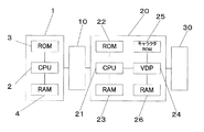
図1は本発明における遊技機の制御装置のブロック図である。主制御装置1は遊技機の遊技全体を制御する制御装置であって、CPU1(本発明の「第1の演算処理手段」に相当する)、ROM3(本発明の「遊技制御プログラム記憶手段」に相当する)、RAM4(本発明の「遊技制御データ一時記憶手段」に相当する)を備えている。
FIG. 1 is a block diagram of a control device for a gaming machine according to the present invention. The
本発明の遊技機においては、所定の遊技条件(例えば「ぱちんこ遊技機」であれば、周知の遊技盤面上に配置された始動入賞口にパチンコ球が入賞したこと)が発生した場合、所謂大当たり遊技を発生させるか否かの抽選を行い、その抽選結果に応じて画像表示装置30で画像表示演出を行うが、この点については周知であるので説明を省略する。
In the gaming machine of the present invention, when a predetermined gaming condition occurs (for example, in the case of a “pachinko gaming machine”, a pachinko ball has been won at a starting winning opening arranged on a well-known gaming board surface), so-called jackpot A lottery is performed as to whether or not a game is to be generated, and an image display effect is provided on the
上記所定の遊技条件が発生すると、主制御装置1は図示しない通信回路を介して演出制御指令信号(コマンド)を副制御装置10に送信する。
When the predetermined game condition occurs, the
演出制御指令信号を受信した副制御装置10は受信した演出制御指令信号に基づいて表示制御指令信号(コマンド)を図示しない通信回路を介して表示制御装置20に送信する。併せて遊技機に搭載された図示しない電飾装置やスピーカーを制御して光および音による演出を行う。
The
表示制御装置20にはCPU21(本発明の「第2の演算処理手段」に相当する)、ROM22(本発明の表示制御プログラム記憶手段)に相当する)、RAM23(本発明の「表示制御用データ一時記憶手段」に相当する)、VDP24(本発明の「画像処理手段」に相当する)、キャラクタROM25(本発明の「画像データ記憶手段」に相当する。)RAM26(本発明の「画像表示用データ一時記憶手段」に相当する)を備える。
The
CPU21は表示制御指令信号を受信するとROM22から表示制御用プログラムを読み出して表示制御を開始し、VDP24に画像処理の実行を指示する。尚、RAM23は表示制御処理のための表示制御用データが一時的に記憶される記憶手段である。
When the
画像処理の実行を指示されたVDP24はその内部の記憶領域(図示せず)に記憶されたプログラムに基づいて画像処理を開始し、画像表示装置30の画面上に表示すべき画像をキャラクタROM25から読み出し、読み出した画像に対して合成処理等の画像処理を施した上で画像表示用のデータをRAM26に一時記憶させ、図示しないD/Aコンバータを介して画像表示用データを画像表示装置30に送信し、画像を表示させる。
The VDP 24 instructed to perform image processing starts image processing based on a program stored in an internal storage area (not shown), and an image to be displayed on the screen of the
図2はVDP24およびキャラクタROM25の内部構成を示す。VDP24はその内部にNAND型フラッシュメモリ制御回路27を備える。NAND型フラッシュメモリ制御回路27はキャラクタROM25に備えられたNAND型フラッシュメモリ29からのデータ読み出しを制御するための回路である。NAND型フラッシュメモリ29からデータを読み出す際にはNAND型フラッシュメモリ制御回路の指示によって複数種類の画像の表示用データを一括で読み出す処理が行われる。一括で読み出された複数種類の画像の表示用データはVDP24に備えられた図示しない内蔵RAM領域に記憶され、VDP24は内蔵RAM領域に記憶された画像表示用データを用いて画像処理を行う。このようにVDP24は複数種類の画像の表示用データを一括してNAND型フラッシュメモリ29から読み出して、読み出した画像表示用データを内蔵RAM領域に記憶し、記憶した画像表示用データを基に画像処理を行うためNAND型フラッシュメモリ29に不良データブロックがあった場合でも調停回路28が後述の方法によりデータアドレスの変換を実行する頻度を下げ、処理負荷を低減させることができる。
FIG. 2 shows the internal configuration of the
本発明のNAND型フラッシュメモリ29におけるデータの記憶方式について図3および4に基づいて説明する。図3は所謂「スワップ方式」の記憶方式について模式的に表したものであり、図4が本発明におけるNAND型フラッシュメモリのデータ記憶方式を同じく模式的に表したものである。
A data storage system in the
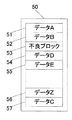
図3においてデータ記憶領域50はデータブロック51〜57に表すように複数のデータブロックで構成されている。ここで仮に画像表示用データはデータA〜Dの4つのデータブロックによって1つの画像データが構成されているものとする。更にそれに続く複数の連続するデータブロックによって複数の画像データが構成されているものとする。図3ではデータブロック51にデータA、データブロック52にデータB、データブロック53は不良ブロックであるためデータが記憶されず、データブロック54にデータD、データブロック57に本来はデータブロック53に記憶されるはずであったデータCが記憶されている。データブロック55に記憶されているデータEとデータブロック56に記憶されているデータZはそれぞれデータA〜Dにより構成されている画像とは別の画像を表示するためのデータである。
In FIG. 3, the
図3の記憶方式ではデータブロック53が不良ブロックであったためデータを書き込むことができず、本来はデータブロック53に記憶されるはずのデータCが離れたアドレスであるデータブロック57に記憶されている。このような場合、VDP24が調停回路28を介してデータA〜Dで構成される画像を読み出そうとすると、まずデータブロック51からデータA、52からデータBを読み出し、次にデータブロック57のアドレスに飛んでデータCを読み出し、もう一度データブロック54のアドレスに戻ってデータDを読み出さなければ1つの画像を表示できない。
In the storage method of FIG. 3, data cannot be written because the
これに対して図4に示す本件発明のデータ記憶方式では、記憶領域40のうちデータブロック41にデータA、データブロック42にデータB、データブロック43は不良ブロックであるためデータが記憶されず、データブロック44にデータC、データブロック45にデータDが記憶されている。また図3の場合と同様にデータブロック46には別の画像のデータであるデータZが記憶されている。
On the other hand, in the data storage method of the present invention shown in FIG. 4, data A is stored in the
図4に示す本発明のデータ記憶方式では不良ブロックであるデータブロック43を除いて画像データが順番に順序よく並んでいる。特に本来データブロック53に記憶されるはずであったデータCは不良ブロックであるデータブロック43の次のデータブロック44に記憶されているのでVDP24が調停回路28を介してデータを読み出す場合にはデータブロック43を読み飛ばすだけで1つの画像を表示するためのデータA〜Dを読み出すことができ、図3の場合のようにデータアドレスを往復するような処理をする必要がなく処理負荷を軽減することができる。
In the data storage system of the present invention shown in FIG. 4, the image data are arranged in order in order except for the data block 43 which is a defective block. In particular, since the data C that should originally be stored in the data block 53 is stored in the data block 44 next to the data block 43 that is a defective block, the data is read when the
図5はVDP24の内蔵ROM領域におけるデータ記憶の方式を示すものである。調停回路28の処理によって図示のようにVDP24の内蔵RAM領域ではデータブロック61〜66の間でデータが整然と並んでいる。前述のようにVDP24が複数の画像データを一括で読み出すことによって調停回路28がデータアドレスを変換する頻度を低下させることができ、処理効率を向上させることができる。
FIG. 5 shows a data storage system in the built-in ROM area of the
尚、本実施例においては「ぱちんこ遊技機」を例にとって説明したが、本発明は「回動式遊技機」の他に所謂「アレンジボール」等「ぱちんこ遊技機」の変種の遊技機であっても、遊技ホールに設置される遊技機で画像表示装置を備えた遊技機であれば適用が可能である。 In the present embodiment, the description has been given by taking the “pachinko gaming machine” as an example. However, the present invention can be applied to any gaming machine installed in a gaming hall and equipped with an image display device.
また、ROM3、RAM4はCPU2に内蔵されているものであっても良く、同様にROM22、RAM23はCPU21に内蔵されるものであっても良い。本発明でいう「接続する」とは配線により外部から接続されるもののみならず、例えば1チップマイコンのように素子の内部でCPUとROM、RAMが接続されているものを含むものである。
The
1 主制御装置
20 表示制御装置
24 画像処理手段
25 画像データ記憶手段
DESCRIPTION OF
Claims (2)
前記遊技機には、前記遊技機の遊技状態を制御する主制御装置と、前記主制御装置から出力された演出制御指令信号に基づいて遊技演出を制御する副制御装置と、前記副制御装置から出力された表示制御指令信号に基づいて前記画像表示装置を制御する表示制御装置と、を備え、
前記主制御装置には、前記演出制御指令処理を行う第1の演算処理手段と、遊技制御プログラムが記憶された遊技制御プログラム記憶手段と、遊技制御データが一時記憶される遊技制御データ一時記憶手段と、を備え、
前記遊技制御プログラム記憶手段と前記遊技制御データ一時記憶手段とを前記第1の演算処理手段に接続し、
前記表示制御装置には、表示制御プログラムを実行する第2の演算処理手段と、前記表示制御プログラムが記憶された表示制御プログラム記憶手段と、表示制御用データが一時記憶される表示制御用データ一時記憶手段と、前記画像表示装置に表示される画像の制御を行う画像処理手段と、前記画像を表示するための画像データが記憶された画像データ記憶手段と、前記画像表示装置に表示される画像の表示用データが一時的に記憶される画像表示データ一時記憶手段とを備え、
前記表示制御プログラム記憶手段および前記表示制御用データ一時記憶手段と前記画像処理手段とを前記第2の演算処理手段に接続するとともに、前記画像データ記憶手段と前記画像表示データ一時記憶手段とを前記画像処理手段に接続し、
前記画像データ記憶手段には、NAND型フラッシュメモリと調停回路とを含み、
前記NAND型フラッシュメモリは、複数のデータブロックで構成されるとともに、前記複数のデータブロック中に不良データブロックが存在する場合、前記不良データブロックの直前のデータブロックに記憶された画像データの次の画像データが前記不良データブロックを避けた状態で前記不良データブロックの直後のデータブロックに記憶され、
前記調停回路は、前記画像処理手段からの画像データ読み出し要求に応じて前記不良データブロックの後のデータブロックに記憶された画像データの先頭アドレスを前記不良データブロックの前のデータブロックに記憶された画像データの最終アドレスの次のアドレスに変換して出力することを特徴とする遊技機。 In a gaming machine equipped with an image display device,
The gaming machine includes a main control device that controls a gaming state of the gaming machine, a sub control device that controls a game effect based on an effect control command signal output from the main control device, and the sub control device. A display control device that controls the image display device based on the output display control command signal,
The main control device includes a first arithmetic processing means for performing the effect control command process, a game control program storage means for storing a game control program, and a game control data temporary storage means for temporarily storing game control data. And comprising
Connecting the game control program storage means and the game control data temporary storage means to the first arithmetic processing means;
The display control device includes a second arithmetic processing means for executing a display control program, a display control program storage means for storing the display control program, and a display control data temporarily storing display control data. Storage means, image processing means for controlling an image displayed on the image display device, image data storage means for storing image data for displaying the image, and an image displayed on the image display device Image display data temporary storage means for temporarily storing display data of
The display control program storage means, the display control data temporary storage means and the image processing means are connected to the second arithmetic processing means, and the image data storage means and the image display data temporary storage means are Connected to the image processing means,
The image data storage means includes a NAND flash memory and an arbitration circuit,
The NAND flash memory is composed of a plurality of data blocks, and when there is a defective data block in the plurality of data blocks, the NAND flash memory is next to the image data stored in the data block immediately before the defective data block. The image data is stored in a data block immediately after the defective data block in a state avoiding the defective data block,
The arbitration circuit stores the start address of the image data stored in the data block after the defective data block in the data block before the defective data block in response to the image data read request from the image processing means. A gaming machine characterized in that it is converted into an address next to the final address of image data and output.
前記画像データ記憶手段から画像データを読み出す際には、複数種類の画像に関するデータを一括して読み出し、
前記一括して読み出した複数種類の画像データを一時記憶して画像処理を行うことを特徴とする請求項1に記載の遊技機。 The image processing means includes a NAND flash memory control circuit that performs a data read command control from the NAND flash memory,
When reading image data from the image data storage means, data relating to a plurality of types of images is read in a batch,
The gaming machine according to claim 1, wherein the plurality of types of image data read in a batch are temporarily stored to perform image processing.
Priority Applications (1)
| Application Number | Priority Date | Filing Date | Title |
|---|---|---|---|
| JP2005041382A JP2006223598A (en) | 2005-02-17 | 2005-02-17 | Game machine |
Applications Claiming Priority (1)
| Application Number | Priority Date | Filing Date | Title |
|---|---|---|---|
| JP2005041382A JP2006223598A (en) | 2005-02-17 | 2005-02-17 | Game machine |
Related Child Applications (1)
| Application Number | Title | Priority Date | Filing Date |
|---|---|---|---|
| JP2011103979A Division JP5165081B2 (en) | 2011-05-09 | 2011-05-09 | Game machine |
Publications (2)
| Publication Number | Publication Date |
|---|---|
| JP2006223598A true JP2006223598A (en) | 2006-08-31 |
| JP2006223598A5 JP2006223598A5 (en) | 2009-12-24 |
Family
ID=36985468
Family Applications (1)
| Application Number | Title | Priority Date | Filing Date |
|---|---|---|---|
| JP2005041382A Pending JP2006223598A (en) | 2005-02-17 | 2005-02-17 | Game machine |
Country Status (1)
| Country | Link |
|---|---|
| JP (1) | JP2006223598A (en) |
Cited By (6)
| Publication number | Priority date | Publication date | Assignee | Title |
|---|---|---|---|---|
| JP2008119341A (en) * | 2006-11-15 | 2008-05-29 | Daiman:Kk | Game machine |
| JP2008228955A (en) * | 2007-03-20 | 2008-10-02 | Daiman:Kk | Game machine |
| JP2010137019A (en) * | 2008-11-17 | 2010-06-24 | Sanyo Product Co Ltd | Game machine |
| JP2012130785A (en) * | 2012-04-09 | 2012-07-12 | Daiichi Shokai Co Ltd | Game machine |
| JP2018202259A (en) * | 2018-10-09 | 2018-12-27 | 株式会社三洋物産 | Slot machine and game machine |
| JP2018202260A (en) * | 2009-06-30 | 2018-12-27 | 株式会社三洋物産 | Game machine |
Citations (8)
| Publication number | Priority date | Publication date | Assignee | Title |
|---|---|---|---|---|
| JPH08314798A (en) * | 1995-05-17 | 1996-11-29 | Seiko Epson Corp | Semiconductor integrated circuit and cartridge for game machine |
| JP2000268194A (en) * | 1999-03-18 | 2000-09-29 | Airemu Software Engineering Kk | Image display method and device and game machine |
| JP2000330876A (en) * | 1999-04-27 | 2000-11-30 | Samsung Electronics Co Ltd | Method for programming memory device |
| JP2001070590A (en) * | 1999-09-07 | 2001-03-21 | Sankyo Kk | Game machine |
| JP2003047729A (en) * | 2001-08-06 | 2003-02-18 | Daidoo:Kk | Game machine |
| JP2004057309A (en) * | 2002-07-25 | 2004-02-26 | Sankyo Kk | Game machine |
| JP2004103162A (en) * | 2002-09-11 | 2004-04-02 | Fujitsu Ltd | Nand type flash memory |
| JP2004154421A (en) * | 2002-11-07 | 2004-06-03 | Daiman:Kk | Malfunction detector for rom |
-
2005
- 2005-02-17 JP JP2005041382A patent/JP2006223598A/en active Pending
Patent Citations (8)
| Publication number | Priority date | Publication date | Assignee | Title |
|---|---|---|---|---|
| JPH08314798A (en) * | 1995-05-17 | 1996-11-29 | Seiko Epson Corp | Semiconductor integrated circuit and cartridge for game machine |
| JP2000268194A (en) * | 1999-03-18 | 2000-09-29 | Airemu Software Engineering Kk | Image display method and device and game machine |
| JP2000330876A (en) * | 1999-04-27 | 2000-11-30 | Samsung Electronics Co Ltd | Method for programming memory device |
| JP2001070590A (en) * | 1999-09-07 | 2001-03-21 | Sankyo Kk | Game machine |
| JP2003047729A (en) * | 2001-08-06 | 2003-02-18 | Daidoo:Kk | Game machine |
| JP2004057309A (en) * | 2002-07-25 | 2004-02-26 | Sankyo Kk | Game machine |
| JP2004103162A (en) * | 2002-09-11 | 2004-04-02 | Fujitsu Ltd | Nand type flash memory |
| JP2004154421A (en) * | 2002-11-07 | 2004-06-03 | Daiman:Kk | Malfunction detector for rom |
Cited By (9)
| Publication number | Priority date | Publication date | Assignee | Title |
|---|---|---|---|---|
| JP2008119341A (en) * | 2006-11-15 | 2008-05-29 | Daiman:Kk | Game machine |
| JP2008228955A (en) * | 2007-03-20 | 2008-10-02 | Daiman:Kk | Game machine |
| JP2010137019A (en) * | 2008-11-17 | 2010-06-24 | Sanyo Product Co Ltd | Game machine |
| JP2013144211A (en) * | 2008-11-17 | 2013-07-25 | Sanyo Product Co Ltd | Game machine |
| JP2015134285A (en) * | 2008-11-17 | 2015-07-27 | 株式会社三洋物産 | Game machine |
| JP2021107030A (en) * | 2008-11-17 | 2021-07-29 | 株式会社三洋物産 | Game machine |
| JP2018202260A (en) * | 2009-06-30 | 2018-12-27 | 株式会社三洋物産 | Game machine |
| JP2012130785A (en) * | 2012-04-09 | 2012-07-12 | Daiichi Shokai Co Ltd | Game machine |
| JP2018202259A (en) * | 2018-10-09 | 2018-12-27 | 株式会社三洋物産 | Slot machine and game machine |
Similar Documents
| Publication | Publication Date | Title |
|---|---|---|
| JP5847971B1 (en) | Game machine | |
| JP2006223598A (en) | Game machine | |
| JP2005087542A (en) | Game machine | |
| JP2012196554A (en) | Game machine | |
| JP5098362B2 (en) | Image display device and game machine | |
| JP5092100B2 (en) | Signal processing system for gaming machines, gaming machines | |
| JP4439939B2 (en) | Game machine | |
| JP2010042299A (en) | Game machine | |
| JP2010181573A (en) | Image processing apparatus, information processing apparatus, mobile terminal device, and image processing method | |
| JP4512733B2 (en) | Game machine | |
| JP2006223598A5 (en) | ||
| JP5165081B2 (en) | Game machine | |
| JP2004236825A (en) | Display control method, display control device and game machine | |
| JP2005208684A (en) | Game machine | |
| JP2011133651A (en) | Setting control device, and method of operating the same | |
| JP2005237711A (en) | Game machine | |
| JP4837059B2 (en) | Game machine | |
| JP2008228955A (en) | Game machine | |
| JP2011050779A (en) | Game machine | |
| JP2021083858A5 (en) | ||
| JP2008079753A (en) | Game machine | |
| JP2005087334A (en) | Game machine | |
| JP2011177390A (en) | Game machine | |
| JP2005218727A (en) | Image display device for game machine | |
| JP2003299848A (en) | Subalternate control device of game machine |
Legal Events
| Date | Code | Title | Description |
|---|---|---|---|
| A621 | Written request for application examination |
Free format text: JAPANESE INTERMEDIATE CODE: A621 Effective date: 20080201 |
|
| A711 | Notification of change in applicant |
Free format text: JAPANESE INTERMEDIATE CODE: A712 Effective date: 20090318 |
|
| A521 | Written amendment |
Free format text: JAPANESE INTERMEDIATE CODE: A523 Effective date: 20091016 |
|
| RD02 | Notification of acceptance of power of attorney |
Free format text: JAPANESE INTERMEDIATE CODE: A7422 Effective date: 20091016 |
|
| A521 | Written amendment |
Free format text: JAPANESE INTERMEDIATE CODE: A821 Effective date: 20091019 |
|
| A977 | Report on retrieval |
Free format text: JAPANESE INTERMEDIATE CODE: A971007 Effective date: 20100922 |
|
| A131 | Notification of reasons for refusal |
Free format text: JAPANESE INTERMEDIATE CODE: A131 Effective date: 20101026 |
|
| A521 | Written amendment |
Free format text: JAPANESE INTERMEDIATE CODE: A523 Effective date: 20101224 |
|
| A131 | Notification of reasons for refusal |
Free format text: JAPANESE INTERMEDIATE CODE: A131 Effective date: 20110308 |
|
| A521 | Written amendment |
Free format text: JAPANESE INTERMEDIATE CODE: A523 Effective date: 20110509 |
|
| A02 | Decision of refusal |
Free format text: JAPANESE INTERMEDIATE CODE: A02 Effective date: 20110816 |