JP2006210941A - Semiconductor device - Google Patents
Semiconductor device Download PDFInfo
- Publication number
- JP2006210941A JP2006210941A JP2006085030A JP2006085030A JP2006210941A JP 2006210941 A JP2006210941 A JP 2006210941A JP 2006085030 A JP2006085030 A JP 2006085030A JP 2006085030 A JP2006085030 A JP 2006085030A JP 2006210941 A JP2006210941 A JP 2006210941A
- Authority
- JP
- Japan
- Prior art keywords
- lead
- back surface
- resin
- resin sealing
- sealing body
- Prior art date
- Legal status (The legal status is an assumption and is not a legal conclusion. Google has not performed a legal analysis and makes no representation as to the accuracy of the status listed.)
- Pending
Links
Images


Classifications
-
- H—ELECTRICITY
- H01—ELECTRIC ELEMENTS
- H01L—SEMICONDUCTOR DEVICES NOT COVERED BY CLASS H10
- H01L24/00—Arrangements for connecting or disconnecting semiconductor or solid-state bodies; Methods or apparatus related thereto
- H01L24/93—Batch processes
- H01L24/95—Batch processes at chip-level, i.e. with connecting carried out on a plurality of singulated devices, i.e. on diced chips
- H01L24/97—Batch processes at chip-level, i.e. with connecting carried out on a plurality of singulated devices, i.e. on diced chips the devices being connected to a common substrate, e.g. interposer, said common substrate being separable into individual assemblies after connecting
-
- H—ELECTRICITY
- H01—ELECTRIC ELEMENTS
- H01L—SEMICONDUCTOR DEVICES NOT COVERED BY CLASS H10
- H01L2224/00—Indexing scheme for arrangements for connecting or disconnecting semiconductor or solid-state bodies and methods related thereto as covered by H01L24/00
- H01L2224/01—Means for bonding being attached to, or being formed on, the surface to be connected, e.g. chip-to-package, die-attach, "first-level" interconnects; Manufacturing methods related thereto
- H01L2224/02—Bonding areas; Manufacturing methods related thereto
- H01L2224/04—Structure, shape, material or disposition of the bonding areas prior to the connecting process
- H01L2224/05—Structure, shape, material or disposition of the bonding areas prior to the connecting process of an individual bonding area
- H01L2224/0554—External layer
- H01L2224/0555—Shape
- H01L2224/05552—Shape in top view
- H01L2224/05554—Shape in top view being square
-
- H—ELECTRICITY
- H01—ELECTRIC ELEMENTS
- H01L—SEMICONDUCTOR DEVICES NOT COVERED BY CLASS H10
- H01L2224/00—Indexing scheme for arrangements for connecting or disconnecting semiconductor or solid-state bodies and methods related thereto as covered by H01L24/00
- H01L2224/01—Means for bonding being attached to, or being formed on, the surface to be connected, e.g. chip-to-package, die-attach, "first-level" interconnects; Manufacturing methods related thereto
- H01L2224/42—Wire connectors; Manufacturing methods related thereto
- H01L2224/44—Structure, shape, material or disposition of the wire connectors prior to the connecting process
- H01L2224/45—Structure, shape, material or disposition of the wire connectors prior to the connecting process of an individual wire connector
- H01L2224/45001—Core members of the connector
- H01L2224/45099—Material
- H01L2224/451—Material with a principal constituent of the material being a metal or a metalloid, e.g. boron (B), silicon (Si), germanium (Ge), arsenic (As), antimony (Sb), tellurium (Te) and polonium (Po), and alloys thereof
- H01L2224/45138—Material with a principal constituent of the material being a metal or a metalloid, e.g. boron (B), silicon (Si), germanium (Ge), arsenic (As), antimony (Sb), tellurium (Te) and polonium (Po), and alloys thereof the principal constituent melting at a temperature of greater than or equal to 950°C and less than 1550°C
- H01L2224/45144—Gold (Au) as principal constituent
-
- H—ELECTRICITY
- H01—ELECTRIC ELEMENTS
- H01L—SEMICONDUCTOR DEVICES NOT COVERED BY CLASS H10
- H01L2224/00—Indexing scheme for arrangements for connecting or disconnecting semiconductor or solid-state bodies and methods related thereto as covered by H01L24/00
- H01L2224/01—Means for bonding being attached to, or being formed on, the surface to be connected, e.g. chip-to-package, die-attach, "first-level" interconnects; Manufacturing methods related thereto
- H01L2224/42—Wire connectors; Manufacturing methods related thereto
- H01L2224/47—Structure, shape, material or disposition of the wire connectors after the connecting process
- H01L2224/48—Structure, shape, material or disposition of the wire connectors after the connecting process of an individual wire connector
- H01L2224/4805—Shape
- H01L2224/4809—Loop shape
- H01L2224/48091—Arched
-
- H—ELECTRICITY
- H01—ELECTRIC ELEMENTS
- H01L—SEMICONDUCTOR DEVICES NOT COVERED BY CLASS H10
- H01L2224/00—Indexing scheme for arrangements for connecting or disconnecting semiconductor or solid-state bodies and methods related thereto as covered by H01L24/00
- H01L2224/01—Means for bonding being attached to, or being formed on, the surface to be connected, e.g. chip-to-package, die-attach, "first-level" interconnects; Manufacturing methods related thereto
- H01L2224/42—Wire connectors; Manufacturing methods related thereto
- H01L2224/47—Structure, shape, material or disposition of the wire connectors after the connecting process
- H01L2224/48—Structure, shape, material or disposition of the wire connectors after the connecting process of an individual wire connector
- H01L2224/481—Disposition
- H01L2224/48151—Connecting between a semiconductor or solid-state body and an item not being a semiconductor or solid-state body, e.g. chip-to-substrate, chip-to-passive
- H01L2224/48221—Connecting between a semiconductor or solid-state body and an item not being a semiconductor or solid-state body, e.g. chip-to-substrate, chip-to-passive the body and the item being stacked
- H01L2224/48245—Connecting between a semiconductor or solid-state body and an item not being a semiconductor or solid-state body, e.g. chip-to-substrate, chip-to-passive the body and the item being stacked the item being metallic
- H01L2224/48247—Connecting between a semiconductor or solid-state body and an item not being a semiconductor or solid-state body, e.g. chip-to-substrate, chip-to-passive the body and the item being stacked the item being metallic connecting the wire to a bond pad of the item
-
- H—ELECTRICITY
- H01—ELECTRIC ELEMENTS
- H01L—SEMICONDUCTOR DEVICES NOT COVERED BY CLASS H10
- H01L2224/00—Indexing scheme for arrangements for connecting or disconnecting semiconductor or solid-state bodies and methods related thereto as covered by H01L24/00
- H01L2224/01—Means for bonding being attached to, or being formed on, the surface to be connected, e.g. chip-to-package, die-attach, "first-level" interconnects; Manufacturing methods related thereto
- H01L2224/42—Wire connectors; Manufacturing methods related thereto
- H01L2224/47—Structure, shape, material or disposition of the wire connectors after the connecting process
- H01L2224/48—Structure, shape, material or disposition of the wire connectors after the connecting process of an individual wire connector
- H01L2224/484—Connecting portions
- H01L2224/48463—Connecting portions the connecting portion on the bonding area of the semiconductor or solid-state body being a ball bond
- H01L2224/48465—Connecting portions the connecting portion on the bonding area of the semiconductor or solid-state body being a ball bond the other connecting portion not on the bonding area being a wedge bond, i.e. ball-to-wedge, regular stitch
-
- H—ELECTRICITY
- H01—ELECTRIC ELEMENTS
- H01L—SEMICONDUCTOR DEVICES NOT COVERED BY CLASS H10
- H01L2224/00—Indexing scheme for arrangements for connecting or disconnecting semiconductor or solid-state bodies and methods related thereto as covered by H01L24/00
- H01L2224/01—Means for bonding being attached to, or being formed on, the surface to be connected, e.g. chip-to-package, die-attach, "first-level" interconnects; Manufacturing methods related thereto
- H01L2224/42—Wire connectors; Manufacturing methods related thereto
- H01L2224/47—Structure, shape, material or disposition of the wire connectors after the connecting process
- H01L2224/49—Structure, shape, material or disposition of the wire connectors after the connecting process of a plurality of wire connectors
- H01L2224/491—Disposition
- H01L2224/4912—Layout
- H01L2224/49171—Fan-out arrangements
-
- H—ELECTRICITY
- H01—ELECTRIC ELEMENTS
- H01L—SEMICONDUCTOR DEVICES NOT COVERED BY CLASS H10
- H01L2924/00—Indexing scheme for arrangements or methods for connecting or disconnecting semiconductor or solid-state bodies as covered by H01L24/00
- H01L2924/01—Chemical elements
- H01L2924/01004—Beryllium [Be]
-
- H—ELECTRICITY
- H01—ELECTRIC ELEMENTS
- H01L—SEMICONDUCTOR DEVICES NOT COVERED BY CLASS H10
- H01L2924/00—Indexing scheme for arrangements or methods for connecting or disconnecting semiconductor or solid-state bodies as covered by H01L24/00
- H01L2924/01—Chemical elements
- H01L2924/01013—Aluminum [Al]
-
- H—ELECTRICITY
- H01—ELECTRIC ELEMENTS
- H01L—SEMICONDUCTOR DEVICES NOT COVERED BY CLASS H10
- H01L2924/00—Indexing scheme for arrangements or methods for connecting or disconnecting semiconductor or solid-state bodies as covered by H01L24/00
- H01L2924/01—Chemical elements
- H01L2924/01014—Silicon [Si]
-
- H—ELECTRICITY
- H01—ELECTRIC ELEMENTS
- H01L—SEMICONDUCTOR DEVICES NOT COVERED BY CLASS H10
- H01L2924/00—Indexing scheme for arrangements or methods for connecting or disconnecting semiconductor or solid-state bodies as covered by H01L24/00
- H01L2924/01—Chemical elements
- H01L2924/01019—Potassium [K]
-
- H—ELECTRICITY
- H01—ELECTRIC ELEMENTS
- H01L—SEMICONDUCTOR DEVICES NOT COVERED BY CLASS H10
- H01L2924/00—Indexing scheme for arrangements or methods for connecting or disconnecting semiconductor or solid-state bodies as covered by H01L24/00
- H01L2924/01—Chemical elements
- H01L2924/01028—Nickel [Ni]
-
- H—ELECTRICITY
- H01—ELECTRIC ELEMENTS
- H01L—SEMICONDUCTOR DEVICES NOT COVERED BY CLASS H10
- H01L2924/00—Indexing scheme for arrangements or methods for connecting or disconnecting semiconductor or solid-state bodies as covered by H01L24/00
- H01L2924/01—Chemical elements
- H01L2924/01078—Platinum [Pt]
-
- H—ELECTRICITY
- H01—ELECTRIC ELEMENTS
- H01L—SEMICONDUCTOR DEVICES NOT COVERED BY CLASS H10
- H01L2924/00—Indexing scheme for arrangements or methods for connecting or disconnecting semiconductor or solid-state bodies as covered by H01L24/00
- H01L2924/01—Chemical elements
- H01L2924/01079—Gold [Au]
-
- H—ELECTRICITY
- H01—ELECTRIC ELEMENTS
- H01L—SEMICONDUCTOR DEVICES NOT COVERED BY CLASS H10
- H01L2924/00—Indexing scheme for arrangements or methods for connecting or disconnecting semiconductor or solid-state bodies as covered by H01L24/00
- H01L2924/10—Details of semiconductor or other solid state devices to be connected
- H01L2924/11—Device type
- H01L2924/14—Integrated circuits
-
- H—ELECTRICITY
- H01—ELECTRIC ELEMENTS
- H01L—SEMICONDUCTOR DEVICES NOT COVERED BY CLASS H10
- H01L2924/00—Indexing scheme for arrangements or methods for connecting or disconnecting semiconductor or solid-state bodies as covered by H01L24/00
- H01L2924/15—Details of package parts other than the semiconductor or other solid state devices to be connected
- H01L2924/181—Encapsulation
Abstract
Description
本発明は、半導体装置及びその製造技術に関し、特に、樹脂封止体の裏面(実装面)に電極部材(リード)を有する半導体装置に適用して有効な技術に関するものである。 The present invention relates to a semiconductor device and a manufacturing technique thereof, and more particularly to a technology effective when applied to a semiconductor device having an electrode member (lead) on the back surface (mounting surface) of a resin sealing body.
半導体チップを樹脂封止体で封止する半導体装置においては、種々なパッケージ構造のものが提案され、実用化されている。例えば、特開平11−330343号公報には、QFN(Quad Flatpack Non-Leaded Package )型と呼ばれる半導体装置が開示されている。このQFN型半導体装置は、半導体チップの電極と電気的に接続された電極部材が樹脂封止体の裏面(実装面)から露出するパッケージ構造になっているため、半導体チップの電極と電気的に接続されたリードが樹脂封止体の側面から突出して所定の形状に折り曲げ成形されたパッケージ構造、例えばQFP(Quad Flatpack Package)型と呼ばれる半導体装置と比較して平面サイズの小型化を図ることができる。 As a semiconductor device for sealing a semiconductor chip with a resin sealing body, various package structures have been proposed and put into practical use. For example, Japanese Patent Application Laid-Open No. 11-330343 discloses a semiconductor device called a QFN (Quad Flatpack Non-Leaded Package) type. Since this QFN type semiconductor device has a package structure in which an electrode member electrically connected to the electrode of the semiconductor chip is exposed from the back surface (mounting surface) of the resin sealing body, it is electrically connected to the electrode of the semiconductor chip. A package structure in which the connected lead protrudes from the side surface of the resin sealing body and is bent into a predetermined shape, such as a semiconductor device called a QFP (Quad Flatpack Package) type, can be reduced in planar size. it can.
QFN型半導体装置は、リードフレームを用いた組立プロセスによって製造される。例えば、ダイパッドに半導体チップを搭載するパッケージ構造の場合、主に、リードフレームのフレーム本体に吊りリードを介して支持されたダイパッド(タブとも言う)に半導体チップを搭載し、その後、半導体チップの電極と、リードフレームのフレーム本体にタイバー(ダムバーとも言う)を介して支持されたリードとをボンディングワイヤで電気的に接続し、その後、半導体チップ、リード、ダイパッド、吊りリード及びボンディングワイヤ等を樹脂封止体で封止し、その後、リードフレームのフレーム本体からリード、タイバー及び吊りリード等を切断分離することによって製造される。ボンディングワイヤの一端側は半導体チップの電極に接続され、その他端側はリードの互いに反対側の主面及び裏面のうちの裏面に接続される。リードの主面は樹脂封止体で覆われ、その裏面は樹脂封止体の互いに反対側の主面及び裏面(実装面)のうちの裏面から露出される。リードフレームのリードは、電極部材として使用される電極部分と、切断工程において除去される除去部分とを有する構成になっており、リードの電極部分から除去部分を切断分離することによって電極部材が形成される。 The QFN type semiconductor device is manufactured by an assembly process using a lead frame. For example, in the case of a package structure in which a semiconductor chip is mounted on a die pad, the semiconductor chip is mainly mounted on a die pad (also referred to as a tab) supported via a suspension lead on the frame body of the lead frame, and then the electrode of the semiconductor chip And a lead supported on the frame body of the lead frame via a tie bar (also referred to as a dam bar) by a bonding wire, and thereafter, a semiconductor chip, a lead, a die pad, a suspension lead and a bonding wire are sealed with a resin. It is manufactured by sealing with a stationary body and then cutting and separating leads, tie bars, suspension leads and the like from the frame body of the lead frame. One end side of the bonding wire is connected to the electrode of the semiconductor chip, and the other end side is connected to the back surface of the main surface and the back surface on the opposite side of the lead. The main surface of the lead is covered with a resin sealing body, and the back surface is exposed from the back surface of the resin sealing body on the opposite main surface and back surface (mounting surface). The lead of the lead frame has a configuration having an electrode portion used as an electrode member and a removed portion removed in the cutting process, and the electrode member is formed by cutting and separating the removed portion from the electrode portion of the lead. Is done.
QFN型半導体装置の樹脂封止体は、大量生産に好適なトランスファ・モールディング法(移送成形法)によって形成される。トランスファ・モールディング法による樹脂封止体の形成は、成形金型のキャビティ(樹脂封止体形成部)の内部に、半導体チップ、リード、ダイパッド、吊りリード及びボンディングワイヤ等が位置するように、成形金型の上型と下型との間にリードフレームを位置決めし、その後、成形金型のキャビティの内部に樹脂を加圧注入することによって行われる。 The resin sealing body of the QFN type semiconductor device is formed by a transfer molding method (transfer molding method) suitable for mass production. The resin molding is formed by the transfer molding method so that the semiconductor chip, lead, die pad, suspension lead, bonding wire, etc. are located inside the mold cavity (resin sealing body forming part). This is done by positioning the lead frame between the upper mold and the lower mold of the mold and then injecting resin into the cavity of the mold.
ところで、樹脂封止体の裏面から電極部材の裏面が露出するパッケージ構造は、成形金型の下型にリードが接するようにリードフレームを成形金型に位置決めし、その後、成形金型のキャビティの内部に樹脂を加圧注入することによって得られるが、この場合、キャビティの内部において、下型とリードとの密着性が低いため、下型とリードとの間に樹脂が入り込み易く、リードの裏面が薄膜状の不要樹脂体(レジンバリ)によって覆われてしまうといった不具合が発生し易い。 By the way, in the package structure in which the back surface of the electrode member is exposed from the back surface of the resin sealing body, the lead frame is positioned on the molding die so that the leads are in contact with the lower die of the molding die. It can be obtained by injecting resin into the inside, but in this case, since the adhesion between the lower mold and the lead is low inside the cavity, the resin can easily enter between the lower mold and the lead. Is likely to be covered with a thin unnecessary resin body (resin burr).
そこで、QFN型半導体装置の製造においては、一般的に、成形金型の下型とリードフレームとの間に樹脂シート(樹脂フィルム)を介在し、この樹脂シートにリードが接するようにリードフレームを成形金型に位置決めし、その後、成形金型のキャビティの内部に樹脂を加圧注入する技術(以下、シートモールド技術と呼ぶ)が採用されている。このシートモールド技術の場合、キャビティの内部において樹脂シートとリードとの密着性が高いため、リードの裏面がレジンバリによって覆われてしまうといった不具合を抑制することができる。シートモールド技術については、例えは、特開平11−274195号公報に開示されている。
本発明者は、QFN型半導体装置について検討した結果、以下の問題点を見出した。
(1)QFN型半導体装置は、実装基板に実装され、この実装基板と共に例えば携帯電話、携帯型情報処理端末機器、携帯型パーソナルコンピュータ等の小型電子機器に組み込まれる。QFN型半導体装置の実装は、一般的にリフローソルダリング(Reflow Soldering)法によって行われる。リフローソルダリング法とは、実装基板の電極上にスクリーン印刷等によって予め施された半田ペースト材を溶融して面実装型電子部品等を半田付けする方法である。
As a result of examining the QFN type semiconductor device, the present inventor has found the following problems.
(1) The QFN type semiconductor device is mounted on a mounting substrate, and is incorporated into a small electronic device such as a mobile phone, a portable information processing terminal device, and a portable personal computer together with the mounting substrate. The QFN type semiconductor device is generally mounted by a reflow soldering method. The reflow soldering method is a method of soldering a surface mount type electronic component or the like by melting a solder paste material applied in advance by screen printing or the like on an electrode of a mounting substrate.
リフローソルダリング法による半田付け実装では、実装基板の電極上に半田ペースト材を施した後、実装基板の実装面上にQFN型半導体装置を自動搭載機で搭載するため、この搭載時において実装基板の電極とQFN型半導体装置の電極部材との間に介在された半田ペースト材が押し潰され、半田ペースト材の一部がQFN型半導体装置の電極部材間(実装基板の電極間)に食み出る(押し出される)。QFN型半導体装置は樹脂封止体の裏面に電極部材を配置したパッケージ構造になっているため、食み(はみ)出た半田ペースト材が広がり易い。食み出た半田ペスト材の広がりが大きくなると、半田ブリッジや、半田ボール等の導電性異物が発生し易くなり、電極間の短絡による実装不良が発生し易くなるため、食み出た半田ペースト材の広がりは極力抑える必要がある。 In solder mounting by the reflow soldering method, a solder paste material is applied to the electrodes of the mounting board, and then the QFN type semiconductor device is mounted on the mounting surface of the mounting board by an automatic mounting machine. Solder paste material interposed between the electrode of the QFN type semiconductor device and the electrode member of the QFN type semiconductor device is crushed, and a part of the solder paste material bites between the electrode members of the QFN type semiconductor device (between the electrodes of the mounting substrate). Go out (push out). Since the QFN type semiconductor device has a package structure in which an electrode member is arranged on the back surface of the resin encapsulant, the solder paste material that has squeezed out easily spreads. If the spread of the solder paste material that protrudes becomes large, conductive foreign matters such as solder bridges and solder balls are likely to be generated, and mounting defects due to short circuits between the electrodes are likely to occur. It is necessary to suppress the spread of the material as much as possible.
食み出た半田ペースト材の広がりを抑えるには、樹脂封止体の裏面よりも電極部材の裏面を突出させたパッケージ構造にし、実装基板の実装面と樹脂封止体の裏面との間の間隔、即ちスタンドオフの高さを高くすることが有効である。食み出た半田ペースト材の広がりによる実装不良の抑制に必要な電極部材の突出高さ(樹脂封止体の裏面から電極部材の裏面までの距離)は、電極部材の配列ピッチや電極部材間の間隔によって異なる。本発明者の検討によれば、電極部材の配列ピッチが0.5mm、電極部材間の間隔が0.3mmの場合、電極部材の突出高さは20μm以上必要であった。 In order to suppress the spread of the protruding solder paste material, the package structure is such that the back surface of the electrode member protrudes from the back surface of the resin sealing body, and between the mounting surface of the mounting substrate and the back surface of the resin sealing body. It is effective to increase the interval, that is, the height of the standoff. The protruding height of the electrode member (distance from the back surface of the resin encapsulant to the back surface of the electrode member) necessary to suppress mounting defects due to the spread of the solder paste material that protrudes is the arrangement pitch of the electrode members and the distance between the electrode members It depends on the interval. According to the study by the present inventors, when the arrangement pitch of the electrode members is 0.5 mm and the distance between the electrode members is 0.3 mm, the protruding height of the electrode members needs to be 20 μm or more.
樹脂封止体の裏面よりも電極部材の裏面を突出させたパッケージ構造(以下、スタンドオフ・パッケージ構造と呼ぶ)は、樹脂封止工程においてシートモールド技術を採用することによって容易に形成することができる。しかしながら、電極部材の突出高さが20μm以上のスタンドオフ・パッケージ構造を得るためには以下に示す問題を対策する必要がある。 A package structure in which the back surface of the electrode member protrudes from the back surface of the resin sealing body (hereinafter referred to as a stand-off package structure) can be easily formed by employing a sheet molding technique in the resin sealing process. it can. However, in order to obtain a standoff package structure in which the protruding height of the electrode member is 20 μm or more, it is necessary to take measures against the following problems.
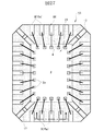
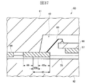
図37及び図38は、従来のQFN型半導体装置の製造における樹脂封止工程(樹脂封止体形成工程)において、成形金型にリードフレームを位置決めした状態を示す模式的断面図、
図39は、図37及び図38の樹脂封止工程において、成型金型にリードフレームを位置決めした状態を示す模式的平面図、
図40は、図39のM−M線に沿う模式的断面図である。なお、図37はリードフレームのリードの部分で切った断面図であり、図38はリードフレームのリード間の部分で切った断面図である。
図37乃至図40において、60は成形金型、61は上型、62は下型、63はキャビティ、64はフレーム本体、65は電極部材として使用される電極部分65aと樹脂封止工程後の切断工程において除去される除去部分65bとを有するリード、66はリード65が一体化されたタイバー、67はダイパッド、68は半導体チップ、69はボンディングワイヤ、70は樹脂シート、71はしわである。
37 and 38 are schematic cross-sectional views showing a state in which a lead frame is positioned in a molding die in a resin sealing step (resin sealing body forming step) in manufacturing a conventional QFN type semiconductor device,
FIG. 39 is a schematic plan view showing a state in which the lead frame is positioned in the molding die in the resin sealing step of FIGS. 37 and 38;
40 is a schematic cross-sectional view taken along line MM in FIG. FIG. 37 is a cross-sectional view taken along a lead portion of the lead frame, and FIG. 38 is a cross-sectional view taken along a portion between the leads of the lead frame.
37 to 40, 60 is a molding die, 61 is an upper die, 62 is a lower die, 63 is a cavity, 64 is a frame body, 65 is an
シートモールド技術による樹脂封止体の形成は、図37乃至図39に示すように、成形金型60の下型62とリードフレームとの間に樹脂シート70を介在し、この樹脂シート70にリード65の互いに反対側の主面及び裏面のうちの裏面が接するようにリードフレームを成形金型60に位置決めし、その後、成形金型60のキャビティ63の内部に樹脂を加圧注入することによって行われる。この樹脂封止工程(樹脂封止体形成工程)において、リードフレームは、フレーム本体64、リード65の電極部分65aの一部及び除去部分65b、タイバー66、並びにこれらの部分と対応する樹脂シート70の部分を上型61の合わせ面と下型62の合わせ面とで上下方向から締め付ける(押さえる)ことによって成形金型60に固定されるため、上型61と下型62との締め付け力(クランプ力)を高めて樹脂シート70を押し潰すことにより、リード65が樹脂シート70に食い(くい)込む。リード65が樹脂シート70に食い込んだ状態でキャビティ63の内部に熱硬化性の樹脂を注入し、その後、樹脂を硬化させることにより、リード65の電極部分65aの裏面が樹脂封止体の裏面よりも突出する。この後、切断工程においてリード65の電極部分65aから除去部分65bを切断分離することにより、リード65の電極部分65aからなる電極部材の裏面が樹脂封止体の裏面よりも突出したオフセット・パッケージ構造になる。電極部材の突出高さはリード65が樹脂シート70に食い込む量(樹脂シートの潰れ量)に依存するため、リード65が樹脂シート70に食い込む量を制御することによって電極部材の突出高さを変えることができる。
As shown in FIGS. 37 to 39, the resin sealing body is formed by sheet molding technology, in which a
しかしながら、本発明者の検討によれば、厚さが40μm程度の薄い樹脂シートを用いて20μmの突出高さを得ようと試みたところ、図40に示すように、隣り合う2つのリード65で挟まれたリード間領域のうち、リード65の除去部分65bで挟まれた領域に樹脂シート70の盛り上がりによるしわ71が発生した。このしわ71の発生メカニズムは以下に示す理由によるものと考える。
However, according to the study of the present inventor, when an attempt was made to obtain a protruding height of 20 μm using a thin resin sheet having a thickness of about 40 μm, as shown in FIG.
リード65を樹脂シート70に食い込ませるためには、タイバー66も樹脂シート70に食い込ませる必要がある。ここで、隣り合う2つのリード65で挟まれたリード間領域において、2つのリード65の電極部分65aで挟まれた領域を第1リード間領域と呼び、2つのリード65の除去部分65bで挟まれた領域を第2リード間領域と呼ぶ。また、タイバー66を連続した一つの構造体と見なし、タイバー66のリード65間における部分をダム部と呼ぶ。
In order for the
リード65で押し潰された樹脂シート70は、第1リード間領域及び第2リード間領域に逃げる。タイバー66で押し潰された樹脂シート70は、第2リード間領域に逃げる。即ち、第2リード間領域には、3方向(2つのリード65側及びタイバー66側)から押し潰された樹脂シート70が集まる(逃げ込む)ため、これらの樹脂シート70の集まりによって、第2リード間領域に盛り上がったしわ71が発生する。この第2リード間領域で発生したしわ71はリード65の延在方向に沿って伸びるため、第2リード間領域で発生したしわ71に起因して第1リード間領域においてもしわ71が発生する。
The
このようなしわ71が発生した状態でキャビティ63の内部に樹脂を注入して樹脂封止体を形成した場合、第1及び第2リード間領域において樹脂封止体にリード65の延在方向に沿う溝が形成される。しわ71は不規則的に形成されるため、図40に示すように、リード65の側面に接するしわ71が発生した場合、リード65の引き抜き強度が低下し、リード65の切断工程等において樹脂封止体からリード65、即ち電極部材が抜けやすくなる。この不具合はQFN型半導体装置の製造歩留まりを著しく低下させる要因となるため、第2リード間領域に発生する樹脂シート70のしわ71を抑制する必要がある。
When a resin sealing body is formed by injecting resin into the
厚い樹脂シート70を用いることでしわ71は発生し難くなるが、樹脂シート70は厚さが厚くなるに従って(使用体積増加に従って)値段が高くなることからコスト上昇につながってしまうため、薄い樹脂シート70でも、しわ71が発生しない様にできる対策が求められる。
(2)QFN型半導体装置においても、樹脂封止体に反りが発生する場合がある。樹脂封止体の裏面が凸面となる方向に反りが発生した場合、実装基板にQFN型半導体装置を実装する時、樹脂封止体の周辺部よりも中央部のスタンドオフが狭くなる。樹脂封止体の裏面から電極部材の裏面が突出する突出高さよりも大きい反りが樹脂封止体に発生した場合、実装基板の電極とQFN型半導体装置の電極部材との半田付けが困難になるため、実装不良を招く要因となる。
The use of the
(2) Even in the QFN type semiconductor device, the resin sealing body may be warped. When warping occurs in the direction in which the back surface of the resin sealing body becomes a convex surface, when the QFN type semiconductor device is mounted on the mounting substrate, the standoff at the center portion becomes narrower than the peripheral portion of the resin sealing body. When warping larger than the protruding height at which the back surface of the electrode member protrudes from the back surface of the resin sealing body occurs in the resin sealing body, it becomes difficult to solder the electrode of the mounting substrate and the electrode member of the QFN type semiconductor device. For this reason, it causes a mounting defect.
本発明の目的は、半導体装置の製造において、樹脂シートのしわを抑制することが可能な技術を提供することにある。 The objective of this invention is providing the technique which can suppress the wrinkle of a resin sheet in manufacture of a semiconductor device.
本発明の目的は、半導体装置の製造歩留まりの向上を図ることが可能な技術を提供することにある。 An object of the present invention is to provide a technique capable of improving the manufacturing yield of a semiconductor device.
本発明の他の目的は、半導体装置の実装不良を抑制することが可能な技術を提供することにある。 Another object of the present invention is to provide a technique capable of suppressing a mounting failure of a semiconductor device.
本発明の前記ならびにその他の目的と新規な特徴は、本明細書の記述及び添付図面によって明らかになるであろう。 The above and other objects and novel features of the present invention will be apparent from the description of this specification and the accompanying drawings.
本願において開示される発明のうち、代表的なものの概要を簡単に説明すれば、下記のとおりである。
(1)互いに反対側の主面及び裏面と、タイバーと、前記タイバーと一体に形成された第1リードと、前記第1リードと間隔をおいて前記タイバーと一体に形成された第2リードとを有するリードフレームを準備すると共に、第1合わせ面及び前記第1合わせ面に連なるキャビティを有する第1型と、前記第1合わせ面と向かい合う第2合わせ面を有する第2型とを有する成形型を準備する工程と、
前記キャビティから前記第1合わせ面に亘って前記第1及び第2リードが位置し、かつ前記タイバー、前記第1及び第2リードの夫々の裏面と前記第2合わせ面との間に樹脂シートが位置するように、前記タイバー、前記第1及び第2リード、並びに前記樹脂シートを前記第1合わせ面と前記第2合わせ面とで夫々の方向から押さえて、前記第1型と前記第2型との間に前記リードフレームを位置決めし、その後、前記キャビティの内部に樹脂を注入して樹脂封止体を形成する工程とを含む半導体装置の製造方法であって、
前記樹脂封止体を形成する工程において、前記第1リードと前記第2リードとの間における前記タイバーの裏面の幅は、前記第1リードと前記第2リードとの間における前記タイバーの主面の幅よりも狭くなっている。
Of the inventions disclosed in this application, the outline of typical ones will be briefly described as follows.
(1) A main surface and a back surface opposite to each other, a tie bar, a first lead formed integrally with the tie bar, and a second lead formed integrally with the tie bar at an interval from the first lead. And a mold having a first mold having a first mating surface and a cavity continuous with the first mating surface, and a second mold having a second mating surface facing the first mating surface The process of preparing
The first and second leads are located from the cavity to the first mating surface, and a resin sheet is interposed between the back surface of each of the tie bar and the first and second leads and the second mating surface. The tie bar, the first and second leads, and the resin sheet are pressed by the first mating surface and the second mating surface from the respective directions so that the first die and the second die are positioned. A step of positioning the lead frame between, and then injecting a resin into the cavity to form a resin sealing body,
In the step of forming the resin sealing body, the width of the back surface of the tie bar between the first lead and the second lead is the main surface of the tie bar between the first lead and the second lead. It is narrower than the width.
(2)前記手段(1)に記載の半導体装置の製造方法において、
前記タイバーの主面及び裏面は、前記第1リードと前記第2リードとの間において、互いに反対側の第1辺及び第2辺を夫々有し、
前記樹脂封止体を形成する工程において、前記タイバーの裏面の第1辺及び第2辺のうちの前記リード側に位置する第1辺は、前記タイバーの主面の第1辺及び第2辺のうちの前記リード側に位置する第1辺よりも前記リードの先端からの距離が遠い位置に配置されている。
(2) In the method for manufacturing a semiconductor device according to the means (1),
The main surface and the back surface of the tie bar each have a first side and a second side opposite to each other between the first lead and the second lead,
In the step of forming the resin sealing body, the first side located on the lead side of the first side and the second side of the back surface of the tie bar is the first side and the second side of the main surface of the tie bar. Of the lead is disposed at a position farther from the tip of the lead than the first side located on the lead side.
(3) 互いに反対側の主面及び裏面と、タイバーと、前記タイバーと一体に形成された第1リードと、前記第1リードと間隔をおいて前記タイバーと一体に形成された第2リードとを有するリードフレームを準備すると共に、第1合わせ面及び前記第1合わせ面に連なるキャビティを有する第1型と、前記第1合わせ面と向かい合う第2合わせ面を有する第2型とを有する成形型を準備する工程と、
前記キャビティから前記第1合わせ面に亘って前記第1及び第2リードが位置し、かつ前記タイバー、前記第1及び第2リードの夫々の裏面と前記第2合わせ面との間に樹脂シートが位置するように、前記タイバー、前記第1及び第2リード、並びに前記樹脂シートを前記第1合わせ面と前記第2合わせ面とで夫々の方向から押さえて、前記第1型と前記第2型との間に前記リードフレームを位置決めし、その後、前記キャビティの内部に樹脂を注入して樹脂封止体を形成する工程とを含む半導体装置の製造方法であって、
前記第1及び第2リードは、前記キャビティから前記第1合わせ面に亘って延在し、かつ電極部材として使用される第1部分と、前記第1部分及び前記タイバーに連なり、かつ切断工程において切断除去される第2部分とを有し、
前記樹脂封止体を形成する工程において、前記第1及び第2リードのうちの少なくとも何れか一方のリードの第2部分における裏面の幅は、前記一方のリードの第2部分における主面の幅よりも狭くなっている。
(3) A main surface and a back surface opposite to each other, a tie bar, a first lead formed integrally with the tie bar, and a second lead formed integrally with the tie bar at an interval from the first lead. And a mold having a first mold having a first mating surface and a cavity continuous with the first mating surface, and a second mold having a second mating surface facing the first mating surface The process of preparing
The first and second leads are located from the cavity to the first mating surface, and a resin sheet is interposed between the back surface of each of the tie bar and the first and second leads and the second mating surface. The tie bar, the first and second leads, and the resin sheet are pressed by the first mating surface and the second mating surface from the respective directions so that the first die and the second die are positioned. A step of positioning the lead frame between, and then injecting a resin into the cavity to form a resin sealing body,
The first and second leads extend from the cavity to the first mating surface and are connected to the first portion used as an electrode member, the first portion and the tie bar, and in a cutting step A second portion to be cut and removed,
In the step of forming the resin sealing body, the width of the back surface of the second portion of at least one of the first and second leads is the width of the main surface of the second portion of the one lead. It is narrower than.
(4)半導体装置は、一主面を有する半導体チップと、
互いに反対側の主面及び裏面を有する電極部材と、
前記半導体チップの電気と前記電極部材の主面とを電気的に接続する接続手段と、
互いに反対側の主面及び裏面を有し、前記半導体チップ、前記電極部材及び前記接続手段を封止する樹脂封止体と、
前記樹脂封止体の裏面から前記樹脂封止体の主面側に向かって窪む凹部とを有し、
前記電極部材の裏面は、前記樹脂封止体の裏面から突出し、
前記凹部の底面から前記電極部材の裏面までの段差は、前記樹脂封止体の裏面から前記電極部材の裏面までの段差よりも大きい。
(4) A semiconductor device includes a semiconductor chip having one main surface;
An electrode member having a main surface and a back surface opposite to each other;
Connection means for electrically connecting the electricity of the semiconductor chip and the main surface of the electrode member;
A resin sealing body having a main surface and a back surface opposite to each other, and sealing the semiconductor chip, the electrode member, and the connection means;
Having a recess recessed from the back surface of the resin sealant toward the main surface of the resin sealant,
The back surface of the electrode member protrudes from the back surface of the resin sealing body,
The step from the bottom surface of the recess to the back surface of the electrode member is larger than the step from the back surface of the resin sealing body to the back surface of the electrode member.
(5)半導体装置の製造方法において、タイバーと一体に形成されたリードを有するリードフレームを準備すると共に、第1型及び第2型を有する成形型であって、前記第1型は、第1合わせ面と、前記第1合わせ面に連なるキャビティとを有し、前記第2型は、前記第1合わせ面と向かい合う第2合わせ面と、前記キャビティと向かい合う位置に配置され、かつ前記第2合わせ面から突出する凸部とを有する成形型を準備する工程と、
前記キャビティから前記第1合わせ面に亘って前記リードが位置し、かつ前記タイバー及び前記リードと前記第2合わせ面との間に樹脂シートが位置するように、前記タイバー、前記リード及び前記樹脂シートを前記第1合わせ面と前記第2合わせ面とで夫々の方向から押さえて、前記樹脂シートに前記リードを食い込ませた状態で、前記第1型と前記第2型との間に前記リードフレームを位置決めし、その後、前記キャビティの内部に樹脂を注入して樹脂封止体を形成する工程とを含む。
(5) In the method of manufacturing a semiconductor device, a lead frame having a lead integrally formed with a tie bar is prepared, and a molding die having a first mold and a second mold is provided. The second mold is disposed at a position facing the first mating surface, a second mating surface facing the first mating surface, and a second mating surface. Preparing a mold having a convex portion protruding from the surface;
The tie bar, the lead, and the resin sheet so that the lead is located from the cavity to the first mating surface, and the resin sheet is located between the tie bar and the lead and the second mating surface. The lead frame is interposed between the first mold and the second mold in a state where the lead is bitten into the resin sheet by pressing the first mating surface and the second mating surface from the respective directions. And then injecting resin into the cavity to form a resin sealing body.
本願において開示される発明のうち代表的なものによって得られる効果を簡単に説明すれば、下記のとおりである。 The effects obtained by the representative ones of the inventions disclosed in the present application will be briefly described as follows.
本発明によれば、半導体装置の製造において、樹脂シートのしわを抑制することができる。 ADVANTAGE OF THE INVENTION According to this invention, the wrinkle of a resin sheet can be suppressed in manufacture of a semiconductor device.
本発明によれば、半導体装置の製造歩留まりの向上を図ることができる。 According to the present invention, it is possible to improve the manufacturing yield of semiconductor devices.
本発明によれば、半導体装置の実装不良を抑制することができる。 According to the present invention, mounting defects of a semiconductor device can be suppressed.
以下、図面を参照して本発明の実施の形態を詳細に説明する。なお、発明の実施の形態を説明するための全図において、同一機能を有するものは同一符号を付け、その繰り返しの説明は省略する。 Hereinafter, embodiments of the present invention will be described in detail with reference to the drawings. Note that components having the same function are denoted by the same reference symbols throughout the drawings for describing the embodiment of the invention, and the repetitive description thereof is omitted.
(実施形態1)
本実施形態ではQFN型半導体装置に本発明を適用した例について説明する。
(Embodiment 1)
In this embodiment, an example in which the present invention is applied to a QFN type semiconductor device will be described.
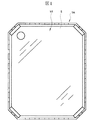
図1は本発明の実施形態1である半導体装置の模式的平面図、
図2は図1に示す半導体装置の模式的底面図、
図3は図1に示す半導体装置の樹脂封止体の上部を除去した状態を示す模式的平面図、
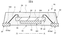
図4は図3のA−A線に沿う模式的断面図、
図5は図4の一部を拡大した模式的断面図、
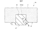
図6は図3のB−B線に沿う模式的断面図、
図7は図6の一部を拡大した模式的断面図である。
FIG. 1 is a schematic plan view of a semiconductor device according to
2 is a schematic bottom view of the semiconductor device shown in FIG.
FIG. 3 is a schematic plan view showing a state where the upper part of the resin sealing body of the semiconductor device shown in FIG. 1 is removed;
4 is a schematic cross-sectional view taken along line AA in FIG.
FIG. 5 is a schematic cross-sectional view enlarging a part of FIG.
6 is a schematic cross-sectional view along the line BB in FIG.
FIG. 7 is an enlarged schematic cross-sectional view of a part of FIG.
図1乃至図4に示すように、本実施形態のQFN型半導体装置1Aは、1つの半導体チップ2、複数の電極部材3、複数のボンディングワイヤ4、1つの樹脂封止体5、1つのダイパッド16、複数の吊りリード17等を有する構成になっている。半導体チップ2、複数の電極部材3、複数のボンディングワイヤ4、ダイパッド16及び複数の吊りリード17等は、樹脂封止体5によって封止されている。
As shown in FIGS. 1 to 4, the QFN
半導体チップ2は互いに反対側の回路形成面(主面)2X及び裏面2Yを有し、回路形成面2Xの平面形状、即ち半導体チップ2の平面形状は方形状で形成されている。本実施形態において、半導体チップ2の平面形状は、例えば1.8mm×2.0mmの長方形で形成されている。半導体チップ2は、例えば、単結晶シリコンからなる半導体基板と、この半導体基板の回路形成面上において絶縁層、配線層の夫々を複数段積み重ねた多層配線層と、この多層配線層を覆うようにして形成された表面保護膜(最終保護膜)とを有する構成になっている。
The
半導体チップ2には、集積回路として例えば制御回路が内蔵されている。この制御回路は、主に、半導体基板の回路形成面に形成されたトランジスタ素子及び多層配線層に形成された配線によって構成されている。
For example, a control circuit is built in the
半導体チップ2の回路形成面2Xには、半導体チップ2の外周囲の各辺に沿って複数の電極(ボンディングパッド)2aが配置されている。この複数の電極2aの夫々は、半導体チップ2の多層配線層のうちの最上層の配線層に形成され、制御回路を構成するトランジスタ素子と電気的に接続されている。複数の電極2aの夫々は、例えば、アルミニウム(Al)膜、若しくはアルミニウムを主体とする合金膜等の金属膜で形成されている。
On the
樹脂封止体5は互いに反対側の主面5X及び裏面(実装面)5Yを有し、主面5Xの平面形状、即ち樹脂封止体5の平面形状は方形状で形成されている。本実施形態において、樹脂封止体5の平面形状は、例えば4.0mm×5.0mmの長方形で形成されている。樹脂封止体5は低応力化を図る目的として、例えば、フェノール系硬化剤、シリコーンゴム及びフィラー等が添加されたエポキシ系の熱硬化性樹脂で形成されている。
The
複数の電極部材3の夫々は、半導体チップ2の外周囲の外側に配置され、樹脂封止体5の外周囲の各辺に沿って配列されている。複数の電極部材3の夫々は、互いに反対側の主面3X及び裏面(実装面)3Yを有する構成になっている。
Each of the plurality of
複数の電極部材3は、半導体チップ2の回路形成面2Xに形成された複数の電極2aにボンディングワイヤ4を介して夫々電気的に接続されている。ボンディングワイヤ4は、一端側が半導体チップ2の電極2aに接続され、他端側が電極部材3の主面3Xに接続されている。ボンディングワイヤ4としては、例えば金(Au)ワイヤを用いている。ボンディングワイヤ4の接続方法としては、例えば、熱圧着に超音波振動を併用したボールボンディング(ネイルヘッドボンディング)法を用いている。
The plurality of
ダイパッド16は互いに反対側の主面16X及び裏面16Yを有する構成になっており、ダイパッド16の主面16Xには接着材を介在して半導体チップ2の裏面2Yが接着されている。ダイパッド16の裏面16Yは、樹脂封止体5の裏面5Yよりも樹脂封止体5の主面5X側に位置し、樹脂封止体5によって覆われている。
The
ダイパッド16は4つの吊りリード17と一体に形成され、4つの吊りリード17は半導体チップ2の4つの角部に夫々配置されている。吊りリード17は、互いに反対側の主面及び裏面を有する構成になっており、更に、ダイパッド16から樹脂封止体5の外周囲に向かって延在する第1部分と、この第1部分から樹脂封止体5の裏面5Y側に折れ曲がる第2部分と、この第2部分から樹脂封止体5の外周囲に向かって延在する第3部分とを有する構成になっている。吊りリード17の第3部分は半導体チップ2の厚さ方向において電極部材3とほぼ同じ高さに配置されている。吊りリード17の第1部分及び第2部分の裏面は樹脂封止体5の裏面5Yよりもその主面5X側に位置し、吊りリード17の第3部分の裏面は樹脂封止体5の裏面5Yから露出している。
The
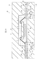
図4及び図5に示すように、複数の電極部材3の夫々の裏面3Yは、樹脂封止体5の裏面5Yから露出している。また、複数の電極部材3の夫々は互いに反対側の先端部及び末端部を有し、先端部は半導体チップ2と向かい合っており、末端部は樹脂封止体5の側面5Zから突出している。また、複数の電極部材3の夫々の主面3Xは樹脂封止体5の裏面5Yよりも樹脂封止体5の主面5X側に位置し、夫々の裏面3Yは樹脂封止体5の裏面5Yから突出している。即ち、本実施形態のQFN型半導体装置1Aはスタンドオフ・パッケージ構造になっている。本実施形態において、電極部材3の突出高さ(樹脂封止体5の裏面5Yから電極部材3の裏面3Yまでの距離)SHは、例えば20μm程度になっている。また、電極部材3は、例えば0.2mm程度の厚さで形成されている。
As shown in FIGS. 4 and 5, the
図6及び図7に示すように、電極部材3の裏面3Yと樹脂封止体5の裏面5Yとは、樹脂封止体5の裏面5Yから電極部材3の裏面3Yが突出する段差面となり、樹脂封止体5の裏面5Yは、電極部材3に向かうに従って途中から徐々に電極部材3の裏面3Yの縁に近づくようにその高さを変える変化面5Y1となっている。変化面5Y1は弧面となり、例えば変化面5Y1の曲率R1は段差高さh1よりも大きくなる円弧となっている。
As shown in FIGS. 6 and 7, the
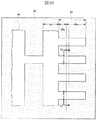
次に、QFN型半導体装置1Aの製造に用いられるリードフレームについて、図8乃至図12を用いて説明する。
図8はリードフレームの一部を示す模式的平面図、
図9は図8の一部を拡大した模式的平面図、
図10は図9の一部を拡大した模式的平面図、
図11は図10の模式的底面図、
図12は、図10の各切断線に沿う模式的断面図であり、(a)はC−C線に沿う模式的断面図、(b)はD−D線に沿う模式的断面図、(c)はE−E線に沿う模式的断面図である。
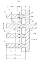
Next, a lead frame used for manufacturing the QFN
FIG. 8 is a schematic plan view showing a part of the lead frame,
FIG. 9 is a schematic plan view enlarging a part of FIG.
FIG. 10 is a schematic plan view enlarging a part of FIG.
FIG. 11 is a schematic bottom view of FIG.
12 is a schematic cross-sectional view taken along each cutting line in FIG. 10, (a) is a schematic cross-sectional view taken along the line CC, (b) is a schematic cross-sectional view taken along the line DD, c) is a schematic cross-sectional view along the line EE.
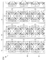
図8及び図9に示すように、リードフレーム10は、フレーム本体11で規定された複数の製品形成領域12を行列状に配置した構成となっている。各製品形成領域12には、複数のリード13、4つのタイバー15、1つのダイパッド16及び4つの吊りリード17等が配置され、更にモールドライン18で囲まれた樹脂封止体形成部が配置されている。
As shown in FIGS. 8 and 9, the
モールドライン18で囲まれた樹脂封止体形成部は本実施形態において長方形の平面形状になっており、この樹脂封止体形成部の外側に4つのタイバー15が配置されている。4つのタイバー15は、樹脂封止体形成部の各辺に対応して配置されており、樹脂封止体形成部の辺に沿って延在し、かつフレーム本体11と一体に形成されている。
The resin sealing body forming portion surrounded by the
複数のリード13は4つのリード群に分割されており、各リード群のリード13は対応するタイバー15と一体に形成されている。各リード群のリード13は、対応するタイバー15の延在方向に沿って所定の間隔をおいて配置されている。各リード群のリード13は、樹脂封止体形成部(モールドライン18)の内外に亘って延在し、互いに反対側の先端部(13c)及び末端部のうちの先端部がダイパッド16と向かい合っている。本実施形態において、リード13は、例えば、0.5mm程度の配列ピッチで配列されている。
The plurality of
ここで、タイバー15を連続した一つの構造体と見なし、タイバー15のリード13間における部分をダム部と呼ぶ。タイバー15のダム部は、トランスファ・モールディング法に基づいて樹脂封止体を形成する際、樹脂がキャビティの外部に漏出するのを防止するためのものである。
Here, the
ダイパッド16は、樹脂封止体形成部の中央部に配置され、4つの吊りリード17を介してフレーム本体11と一体に形成されている。4つの吊りリード17は、樹脂封止体形成部の内外に亘って延在し、互いに反対側の一端側及び他端側のうちの一端側がダイパッド16と一体化され、他端側がフレーム本体11と一体化されている。4つの吊りリード17は、ダイパッド16から樹脂封止体形成部の外周囲(モールドライン18)に向かって延在する第1部分と、この第1部分からリードフレーム10の互いに反対側の主面及び裏面のうちの裏面側に折れ曲がる第2部分と、この第2部分から樹脂封止体形成部の内外に亘って延在する第3部分とを有する構成になっている。吊りリード17の第3部分はリードフレーム10の厚さ方向においてリード13とほぼ同じ高さに位置し、吊りリード17の第1部分及びダイパッド16はリードフレーム10の厚さ方向においてリード13よりもリードフレーム10の主面側に位置している。なお、リード13は、樹脂封止工程後の切断工程において、樹脂封止体形成部の外側に設定された切断ライン19に沿って切断される。
The
図10乃至図12に示すように、リード13は互いに反対側の主面13X及び裏面13Yを有し、更に、電極部材として使用される電極部分(第1部分)13aと、切断工程において除去される除去部分13bとを有する構成になっている。電極部分13aは、樹脂封止体形成部(モールドライン18)の内外に亘って延在し、除去部分13bは樹脂封止体形成部の外側において電極部分13a及びタイバー15に連なっている。図2乃至図7に示す電極部材3は、リード3の電極部分13aから除去部分13bを切断分離することによって形成される。
As shown in FIGS. 10 to 12, the
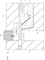
リード13において、電極部分13aは、全体的に、一主面13Xの幅13XW1と裏面13Yの幅13YW1とがほぼ同じ寸法(13XW1≒13YW1)で構成されている。これに対し、除去部分13bは、主面13Xの幅13XW2よりも裏面13Yの幅13YW2が狭い部分(13XW2>13YW2)を有する構成になっている。即ち、電極部分13aでは主面3Xの面積と裏面13Yの面積とがほぼ同一になっているが、除去部分13bでは主面3Xの面積よりも裏面13Yの面積の方が小さくなっている。本実施形態において、電極部分13aの主面13Xの幅13XW1及び裏面13Yの幅13YW1は、例えば0.2mm程度に設定されている。除去部分13bの主面13Xの幅13XW2は全体的に電極部分13aの主面13Xの幅13XW1と同じ寸法に設定されている。除去部分13bの裏面13Yの一部分における幅13YW2は例えば0.1mm程度に設定され、他の部分における幅は主面13Xの幅13XW2と同じ寸法に設定されている。なお、ここで説明しているリード13の各部分の幅とは、リード13の配列方向S1に沿う長さのことである。
In the
タイバー15は、互いに反対側の主面15X及び裏面15Yを有する構成になっている。タイバー15の主面15Xは、全体的にほぼ同一の幅15XWで構成されている。これに対し、タイバー15の裏面15Yは、部分的に主面15Xの幅15XWよりも狭い幅15YWを有する構成となっている。本実施形態において、タイバー15のダム部(互いに隣り合う一方のリード3と他方のリード3との間における部分)は、主面15Xの幅15XWよりも裏面15Yの幅15YWが狭くなっている(15XW>15YW)。即ち、タイバー15のリード13間におけるダム部では、主面15Xの面積よりも裏面15Yの面積が小さくなっている。本実施形態において、タイバー15のダム部は、例えば、主面15Xの幅15XWが0.4mm程度、裏面15Yの幅15YWが0.2mm程度に設定されている。なお、ここで説明しているタイバー15の各部分の幅とは、リード13の配列方向S1と直行する方向S2に沿う長さのことである。
The
除去部分13bの一部分は、リード13の延在方向と直行する断面がV字型になっている。この除去部分13bの一部分において、裏面13Yの互いに反対側の2つの辺(13Y1,13Y2)のうちの一方の辺13Y1は、主面13Xの互いに反対側の2つの辺(13X1,13X2)のうち、リード13の厚さ方向において一方の辺13Y1と反対側に位置する一方の辺13X1よりも内側に位置し、裏面13Yの他方の辺13Y2は、リード13の厚さ方向において他方の辺13Y2と反対側に位置する他方の辺13X2よりも内側に位置している。即ち、除去部分13bの一部分では、主面3Xにおけるリード間の間隔W1よりも裏面3Yにおけるリード間の間隔W2の方が広くなっている。
A portion of the removed
タイバー15のダム部において、裏面15Yの互いに反対側の2つの辺(15Y1,15Y2)のうちのリード13側に位置する一方の辺15Y1とリード13の先端部13cとの間の距離L2は、主面15Xの互いに反対側の2つの辺(15X1,15X2)のうちのリード13側に位置する一方の辺15X1とリード13の先端部13cとの間の距離L1よりも広くなっている。即ち、裏面15Yのリード13側に位置する一方の辺15Y1は、一主面15Xのリード13側に位置する一方の辺15X1よりも、リード13の先端部13cとの距離が長い位置に配置されている。
In the dam portion of the
このような構成のリードフレーム10は、金属板にエッチング加工を施して所定のリードパターンを形成し、その後、吊りリード17に折り曲げ加工を施すことによって形成される。本実施形態のリードフレーム10としては、例えば、銅(Cu)若しくはCu系の合金材からなる金属板にエッチング加工及び折り曲げ加工を施して形成されたリードフレームが用いられている。Cu及びCu系の合金材は、リードフレームの材料として用いられる鉄(Fe)−ニッケル(Ni)系の合金材よりも導電性及び熱導電性に優れているが、このFe−Ni系の合金材よりも機械的強度が低い。おな、リードフレーム10の厚さtは、例えば0.2mm程度に設定されている。
The
ここで、隣り合う2つのリード13で挟まれたリード間領域において、2つのリード13の電極部分13aで挟まれた領域を第1リード間領域14aと呼び、2つのリード13の除去部分13bで挟まれた領域を第2リード間領域14bと呼ぶ。
Here, in a region between the leads sandwiched between two
次に、QFN型半導体装置1Aの製造に用いられる成形金型について、図13を用いて説明する。図13は、成形金型の概略構成を示す模式的断面図である。
Next, a molding die used for manufacturing the QFN
図13に示すように、成形金型20は、これに限定されないが、上下に分割された上型21及び下型22を有し、更に、ポット、カル部、ランナー、樹脂注入ゲート、キャビティ23、エアーベント等を有する構成となっている。上型21は、合わせ面(第1合わせ面)21aと、この合わせ面21aに連なるキャビティ23と、このキャビティ23に樹脂注入ゲートを介して一端側が連なるランナーと、このランナーの他端側に連なるカル部と、このカル部に連なるポット部と、キャビティ23に連なるエアーベントとを有し、下型22は、上型21の合わせ面21a及びキャビティ23と向かい合う合わせ面(第2合わせ面)22aを有する構成になっている。キャビティ23は、上型21の合わせ面21aから上型21の深さ方向に窪んだ構成になっており、その平面形状は方形状になっている。
As shown in FIG. 13, the molding die 20 is not limited to this, but has an
シートモールド技術による樹脂封止体の形成では、成形金型20の下型22とリードフレーム10との間に樹脂シート(樹脂フィルム)30が位置するように、成形金型20の上型21と下型22との間にリードフレーム10を位置決めし、その後、ポットからカル部、ランナー及び樹脂注入ゲートを通してキャビティ23の内部に樹脂を加圧注入することによって行われる。シートモールド技術では、一般的に熱硬化性の樹脂が用いられるため、樹脂シート30としては樹脂封止体形成時の温度に耐える耐熱性の樹脂シートを用いる。また、スタンドオフ・パッケージ構造にするには、成形金型20のクランプ力(締め付け力)によってリードフレームのリードを樹脂シートに食い込ませる必要があるため、成形金型20のクランプ力で容易に潰すことが可能な柔軟性のある樹脂シート(可撓性樹脂シート)を用いる。
In the formation of the resin sealing body by the sheet molding technique, the
次に、QFN型半導体装置1Aの製造について、図14乃至図20を用いて説明する。
図14は、チップボンディング工程及びワイヤボンディング工程が施された状態を示す模式的断面図、
図15は、樹脂封止工程において、成形金型にリードフレームを位置決めした状態を示す模式的断面図、
図16は、樹脂封止工程において、成型金型にリードフレームを位置決めした状態を示す模式的平面図、
図17は、図16のF−F線に沿う模式的断面図、
図18は、図16のG−G線に沿う模式的断面図、
図19は、樹脂封止工程が施された状態を示す模式的断面図、
図20は、樹脂封止工程後の切断工程を説明するための模式的断面図である。
Next, the manufacture of the QFN
FIG. 14 is a schematic cross-sectional view showing a state where the chip bonding process and the wire bonding process have been performed,
FIG. 15 is a schematic cross-sectional view showing a state in which the lead frame is positioned in the molding die in the resin sealing step;
FIG. 16 is a schematic plan view showing a state in which the lead frame is positioned in the molding die in the resin sealing step;
17 is a schematic cross-sectional view taken along line FF in FIG.
18 is a schematic cross-sectional view taken along the line GG in FIG.
FIG. 19 is a schematic cross-sectional view showing a state where the resin sealing step has been performed,
FIG. 20 is a schematic cross-sectional view for explaining the cutting step after the resin sealing step.
まず、図8乃至図12に示すリードフレーム10を準備し、その後、チップボンディング装置(チップボンディング工程)にリードフレーム10を搬送し、図14に示すように、リードフレーム10のダイパッド16の主面16X上に接着材を介在して半導体チップ2を接着固定する。半導体チップ2の接着固定は、半導体チップ2の裏面2Yがダイパッド15の主面15Xと向かい合う状態で行う。
First, the
次に、チップボンディング装置からワイヤボンディング装置(ワイヤボンディング工程)にリードフレーム10を搬送し、図14に示すように、半導体チップ2の複数の電極2aと、リードフレーム10の複数のリード13とを複数のボンディングワイヤ4で夫々電気的に接続する。ボンディングワイヤ4は、一端側が半導体チップ2の電極2aに接続され、他端側がリード13の電極部分13aにおける主面13Xに接続される。
Next, the
次に、ワイヤボンディング装置からトランスファ・モールディング装置(樹脂封止工程)にリードフレーム10を搬送し、図15及び図16に示すように、成形金型20の上型21と下型22との間にリードフレーム10を位置決めする。
Next, the
リードフレーム10の位置決めは、リードフレーム10の裏面(リード13の裏面13Yと同一側の面)と下型22の合わせ面22aとの間に樹脂シート30が介在する状態で行われる。樹脂シート30としては、例えば40μm程度の厚さの樹脂シートを用いる。
また、リードフレーム10の位置決めは、キャビティ23の内部に、半導体チップ2、ボンディングワイヤ4、リード13、ダイパッド16及び吊りリード17等が位置する状態で行われる。
また、リードフレーム10の位置決めは、キャビティ23から上型21の合わせ面21aに亘ってリード13の電極部分13aが位置し、リード13の電極部分13aの一部及び除去部分13b、並びにタイバー15が上型21の合わせ面21aと下型22の合わせ面22aとの間に位置する状態で行われる。
また、リードフレーム10の位置決めは、リード13の電極部分13aの一部及び除去部分13b、タイバー15、並びに、これらの部分に対応する樹脂シート30の部分を上型20の合わせ面21aと下型22の合わせ面22bとで上下方向から締め付ける(押さえる)ことによって行われる。
また、リードフレーム10の位置決めは、リード13が樹脂シート30に食い込むように、上型21と下型22との締め付け力(クランプ力,挟み力)によって樹脂シート30を潰した状態で行われる。本実施形態では、リード13の食い込み量(樹脂シート30の潰れ量)は、例えば20μm程度に設定される。
The positioning of the
The
The
Further, the positioning of the
The
この工程において、タイバー15のダム部(リード13間における部分)は、図10乃至図12に示すように、主面15Xの幅15XWよりも裏面15Yの幅15YWが狭くなっている(15XW>15YW)ことから、図16及び図17に示すように、タイバー15のダム部と樹脂シート30との接触面積が小さくなり、タイバー15のダム部によって潰される樹脂シート30の範囲が狭くなるため、タイバー15のダム部によって潰された樹脂シート30が第2リード間領域(リード13の除去部分13b間)14bに逃げる量を減らすことができる。この結果、リード13の除去部分13bで挟まれた第2リード間領域14bに発生する樹脂シート30のしわを抑制することができる。
また、第2リード間領域14bに発生する樹脂シート30のしわを抑制することができるため、第2リード間領域14bからリード13の電極部分13aで挟まれた第1リード間領域14aに伸びる樹脂シート30のしわを抑制することができる。
In this step, as shown in FIGS. 10 to 12, the dam portion (the portion between the leads 13) of the
Further, since the wrinkle of the
また、タイバー15のダム部(リード13間における部分)において、裏面15Yのリード側に位置する辺15Y1は、図10乃至図12に示すように、主面15Xのリード側に位置する辺15X1よりも、リード13の先端部13cからの距離が遠くなる位置に配置されていることから、タイバー15のダム部によって潰される樹脂シート30の部分が第1リード間領域14aから遠ざかるため、たとえ第2リード間領域14bに樹脂シート30のしわが発生しても、第1リード間領域14aに伸びる樹脂シート30のしわを抑制することができる。
Further, in the dam portion (the portion between the leads 13) of the
また、リード13の除去部分13bの一部分は、図10乃至図12に示すように、主面13Xの幅13XWよりも裏面13Yの幅13YWの方が狭くなっていることから、図16及び図18に示すように、リード13の除去部分13bと樹脂シート30との接触面積が狭くなり、リード13の除去部分13bによって潰される樹脂シート30の範囲が狭くなるため、リード13の除去部分13bで潰された樹脂シート30が第2リード間領域14bに逃げる量を減らすことができる。この結果、リード13の除去部分13bで挟まれた第2リード間領域14bに発生する樹脂シート30のしわを抑制することができる。
また、第2リード間領域14bに発生する樹脂シート30のしわを抑制することができるため、第2リード間領域14bからリード13の電極部分13aで挟まれた第1リード間領域14aに伸びる樹脂シート30のしわを抑制することができる。
Further, as shown in FIGS. 10 to 12, a part of the removed
Further, since the wrinkle of the
次に、前述のようにリードフレーム10を位置決めした状態で、成形金型20のポットからカル部、ランナー及び樹脂注入ゲートを通してキャビティ23の内部に例えば熱硬化性の樹脂を加圧注入して、図19に示すように樹脂封止体5を形成する。半導体チップ2、ボンディングワイヤ4、リード13、ダイパッド16、吊りリード17等は、樹脂封止体5によって封止される。
Next, with the
この工程において、樹脂の充填が終了した後、注入時の圧力よりも高い圧力を加えて樹脂中に巻き込まれたボイドを小さくする工程が施される。この工程は、樹脂中に巻き込まれたボイドを温度サイクル試験時においてポップコーン現象を起こさない程度まで小さくするためである。 In this step, after the filling of the resin is completed, a step of applying a pressure higher than the pressure at the time of injection to reduce the voids caught in the resin is performed. This step is for reducing the voids involved in the resin to such an extent that the popcorn phenomenon does not occur during the temperature cycle test.
また、樹脂封止体5の裏面5Yからリード13の裏面13Yが突出する突出高さが20μm程度のスタンドオフ・パッケージがほぼ完成する。
Further, a stand-off package having a protruding height of about 20 μm from which the
また、リードフレーム10の位置決めにおいて、第2リード間領域14bにおける樹脂シート30のしわが抑制されているため、樹脂シート30のしわに起因して樹脂封止体に形成される溝等の不具合は発生しない。
Further, in the positioning of the
次に、リードフレーム10に貼り付いた樹脂シート30を剥がして成形金型20からリードフレーム10を取り出し、その後、樹脂封止体5の硬化を促進するキュア工程を施した後、切断装置(切断工程)にリードフレーム10を搬送する。この切断工程では、図20に示すように、樹脂封止体5の側面から外側に導出したリード13の電極部分13aの一部及びフレーム本体11を切断金型40のパンチガイド41と受け台42とで上下方向から押さえた後、パンチガイド41側から受け台42側に向かってカットパンチ43を降下し、このカットパンチ43と受け台42による剪断動作によって、リード13の除去部分13b及びタイバー15をフレーム本体11から切断分離する。これにより、リード13の電極部分13aからなる電極部材3が形成される。
Next, the
この後、他の切断工程において、リードフレーム10のフレーム本体11から吊りリート17を切断分離することにより、本実施形態のQFN型半導体装置1Aがほぼ完成する。
Thereafter, in another cutting process, the
次に、QFN型半導体装置1Aの実装について、図21及び図22を用いて説明する。図21及び図22は実装工程を説明するための模式的断面図である。
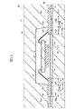
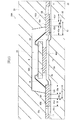
Next, mounting of the QFN
QFN型半導体装置1Aの実装はリフローソルダリング法によって行われる。具体的には、図21に示すように、実装基板50の実装面の電極51上に半田ペースト材52を例えばスクリーン印刷等で施し、その後、実装基板50の電極51とQFN型半導体装置1Aの電極部材3とが互いに向かい合うように位置決めして、実装基板50の実装面上にQFN型半導体装置1Aを自動搭載機で搭載し、その後、半田ペースト材52を溶融して実装基板50の電極51とQFN型半導体装置1Aの電極部材3とを半田付けする。この実装工程において、QFN型半導体装置1Aは自動搭載機によって実装基板50の実装面上に搭載されるため、この搭載時において実装基板50の電極51とQFN型半導体装置1Aの電極部材3との間に介在された半田ペースト材52が押し潰され、図22に示すように、半田ペースト材52の一部がQFN型半導体装置1Aの電極部材3間(実装基板の電極間)に食み出る(押し出される)。この時、QFN半導体装置1Aは、樹脂封止体5の裏面5Yから電極部材3の裏面3Yが突出するスタンドオフ・パッケージ構造になっていることから、食み出た半田ペースト材52は樹脂封止体5の裏面5Yと電極部材3の裏面3Yとの段差部に溜まるため、食み出た半田ペースト材52の広がりを抑制することができる。
The QFN
また、樹脂封止体5の裏面5Yは、電極部材3に向かうに従って途中から徐々に電極部材3の裏面3Yの縁に近づくようにその高さを変える変化面5Y1となっていることから、この変化面5Y1に沿って半田ペースト材52が食み出るため、食み出た半田ペースト材52と樹脂封止体5との間に空気の巻き込みによって発生するボイドを抑制することができる。
Moreover, since the
以上説明したように本実施形態によれば、以下の効果が得られる。
(1)QFN型半導体装置1Aの製造における樹脂封止工程において、タイバー15のダム部(リード13間における部分)は、主面15Xの幅15XWよりも裏面15Yの幅15YWが狭くなっている(15XW>15YW)。これにより、タイバー15のダム部と樹脂シート30との接触面積が小さくなり、タイバー15のダム部によって潰される樹脂シート30の範囲が狭くなるため、タイバー15のダム部によって潰された樹脂シート30が第2リード間領域(リード13の除去部分13b間)14bに逃げる量を減らすことができる。この結果、リード13の除去部分13bで挟まれた第2リード間領域14bに発生する樹脂シート30のしわを抑制することができる。
As described above, according to the present embodiment, the following effects can be obtained.
(1) In the resin sealing step in the manufacture of the QFN
また、第2リード間領域14bに発生する樹脂シート30のしわを抑制することができるため、第2リード間領域14bからリード13の電極部分13aで挟まれた第1リード間領域14aに伸びる樹脂シート30のしわを抑制することができる。
Further, since the wrinkle of the
また、第2リード間領域14bから第1リード間領域14aに伸びる樹脂シート30のしわを抑制することができるため、第1リード間領域14aに発生する樹脂シート30のしわに起因して樹脂封止体5の裏面5Yのリード13間に形成される溝等の不具合を抑制することができる。この結果、溝に起因するリード13の引き抜き強度の低下を抑制でき、リード13の切断工程において樹脂封止体5からリード13、即ち電極部材3が抜けるといった不具合を抑制することができるため、QFN型半導体装置1Aの製造歩留まりの向上を図ることができる。また、実装に対する信頼性の高いQFN型半導体装置1Aを提供することができる。
(2)QFN型半導体装置1Aの製造における樹脂封止工程において、タイバー15のダム部は、裏面15Yのリード側に位置する辺15Y1が、主面15Xのリード側に位置する辺15X1よりも、リード13の先端部13cから、換言すればリード13の電極部分13aと除去部分13bとの間の切断ライン19から遠ざかる位置に配置されている。これにより、タイバー15のダム部によって潰される樹脂シート30の部分が第1リード間領域14aから遠ざかるため、たとえ第2リード間領域14bに樹脂シート30のしわが発生しても、第1リード間領域14aに伸びる樹脂シート30のしわを抑制することができる。
(3)QFN型半導体装置1Aの製造における樹脂封止工程において、リード13の除去部分13bの一部分は、一主面13Xの幅13XWよりも裏面13Yの幅13YWの方が狭くなっている。これにより、リード13の除去部分13bと樹脂シート30との接触面積が狭くなり、リード13の除去部分13bによって潰される樹脂シート30の範囲が狭くなるため、リード13の除去部分13bで潰された樹脂シート30が第2リード間領域14bに逃げる量を減らすことができる。この結果、リード13の除去部分13bで挟まれた第2リード間領域14bに発生する樹脂シート30のしわを抑制することができる。
Further, since wrinkles of the
(2) In the resin sealing step in the manufacture of the QFN
(3) In the resin sealing process in the manufacture of the QFN
また、第2リード間領域14bに発生する樹脂シート30のしわを抑制することができるため、第2リード間領域14bからリード13の電極部分13aで挟まれた第1リード間領域14aに伸びる樹脂シート30のしわを抑制することができる。
Further, since the wrinkle of the
また、第2リード間領域14bから第1リード間領域14aに伸びる樹脂シート30のしわを抑制することができるため、前述のタイバー15の場合と同様に、樹脂シート30のしわに起因して樹脂封止体5の裏面5Yのリード13間に形成される溝によって樹脂封止体5からリード13(電極部材3)が抜けるといった不具合の発生を抑制できる。この結果、QFN型半導体装置1Aの製造歩留まりの向上を図ることができる。また、実装に対する信頼性の高いQFN型半導体装置1Aを提供することができる。
(4)QFN型半導体装置1Aの製造における樹脂封止工程において、厚さが40μm程度の薄い樹脂シート30を使用し、この樹脂シート30にリード13を20μm程度食い込ませても、第1リード間領域14aに樹脂シート30のしわを発生させることなく、樹脂封止体5を形成することができるため、厚い樹脂シートを使用した場合と比較して、電極部材3の突出高さSHが高い20μm以上のQFN型半導体装置を低コストで提供することができる。
(5)実装基板50の実装面上にQFN型半導体装置1Aをリフローソルダリング法で半田付け実装する際、実装基板50の電極51とQFN型半導体装置1Aの電極部材3との間に介在された半田ペースト材52はQFN型半導体装置1Aの自重や搭載機による圧着等によって押し潰され、一部がQFP型半導体装置1Aの電極部材3間(実装基板50の電極51間)に食み(はみ)出るが、QFN型半導体装置1Aは電極部材3の突出高さSHが高い20μm程度のスタンドオフ・パッケージ構造になっていることから、食み出たペースト材52を電極部材3の側面部に溜め込むマージンが大きいため、食み出た半田ペースト材52の広がりを抑制することができる。この結果、半田ブリッジや、半田ボール等導電性異物の発生を抑制できるため、QFN型半導体装置1Aの実装不良を低減することができる。
(6)QFN型半導体装置1Aにおいて、樹脂封止体5の裏面5Yは、電極部材3に向かうに従って途中から徐々に電極部材3の裏面3Yの縁に近づくようにその高さを変える変化面5Y1となっていることから、この変化面5Y1に沿って半田ペースト材52が食み出るため、食み出た半田ペースト材52と樹脂封止体5との間に空気の巻き込みによって発生するボイドを抑制することができる。また、半田ペースト材52をスムーズに潰すことができるため、安定したペースト形状にすることができる。
Further, since the wrinkles of the
(4) In the resin sealing process in the manufacture of the QFN
(5) When the QFN
(6) In the QFN
ところで、第2リード間領域14bから第1リード間領域14aに伸びる樹脂シート30のしわは、リード13の除去部分13bの長さを長くして第1リード間領域14aからタイバー15を遠ざけることでも抑制することができる。しかしながら、この場合、成形金型20を変更する必要があり、更に、1枚のリードフレーム10から取得できる製品の数が減ってしまうため、製造コストの増加を招いてしまう。これに対し、本実施形態では、成形金型20を変更する必要が無く、しかも一枚のリードフレーム20から取得できる製品の数を減らすことなく、第2リード間領域14bから第1リード間領域14aに伸びる樹脂シート30のしわを抑制することができる。
By the way, the wrinkle of the
また、第2リード間領域14bから第1リード間領域14aに伸びる樹脂シート30のしわは、タイバー15の主面及び裏面の幅を両方とも狭くして全体的に細くすることによっても抑制することができる。しかしながら、この場合、タイバー15のダム部の幅方向(リード13の配列方向S1と直行する方向S2)の機械的極度(剛性)が低下してしまうため、キャビティ23の内部に樹脂を加圧注入する時の圧力や、樹脂中に巻き込まれたボイドを小さくするために注入時の圧力よりも高い圧力を加えた時に、タイバー15のダム部がキャビティ23の外側に曲がり易くなるため、タイバー15のダム部から樹脂が漏れるといった不具合が発生し易くなる。これに対し、本実施形態では、ダムバー15を全体的に細くするのではなく、タイバー15のダム部における裏面15Yの幅15YWだけを狭くしているため、タイバー15のダム部の幅方向の機械的強度をほぼ維持したまま、第2リード間領域14bから第1リード間領域14aに伸びる樹脂シート30のしわを抑制することができる。特に、Cu及びCu系の合金材は、Fe−Ni系の合金材よりも機械的強度が低いため、CuやCu系の合金材からなるリードフレームを用いる場合には有用である。
Further, the wrinkles of the
また、第2リード間領域14bから第1リード間領域14aに伸びる樹脂シート30のしわは、リード13の切断部分13bの一部分における主面及び裏面の幅を両方とも狭くして全体的に細くすることによっても抑制することができる。しかしながら、この場合、リード13の切断部分13bの幅方向(リード13の配列方向S1)の機械的強度が低下してしまうため、リード13が根本部分から曲がりやすくなる。これに対し、本実施形態では、リード13の除去部分13bの一部分における幅を全体的に細くするのではなく、リード13の除去部分13bの一部分における幅だけを狭くしているため、リード13の除去部分13bの幅方向の機械的強度をほぼ維持したまま、第2リード間領域14bから第1リード間領域14aに伸びる樹脂シート30のしわを抑制することができる。
Further, the wrinkles of the
なお、本実施形態では、リード13の除去部分13bの一部分において裏面13Yの幅を狭くした例について説明したが、除去部分13bの全体に亘って裏面13Yの幅を狭くしてもよい。
In this embodiment, the example in which the width of the
また、本実施形態では、全てのリード13において除去部分13bの裏面3Yの幅を狭くした例について説明したが、互いに隣り合う2つのリード13において、少なくとも何れか一方のリード13の除去部分13bにおける裏面13Yの幅を狭くしてもよい。即ち、リード13の除去部分13bにおける裏面13Yの幅を狭くする構成は、1本毎に行っても良い。但し、この場合、リード13の除去部分13bで潰された樹脂シート30が第2リード間領域14bに逃げる量を減らせるのは何れか一方のリード側だけとなるため、樹脂シート30のしわを抑制する効果は半減する。
In the present embodiment, the example in which the width of the
また、本実施形態では、タイバー15のダム部全体において、主面15Xの幅15XWよりも裏面15Yの幅15YWを狭くした構成について説明したが、ダム部全体ではなく、図23(半導体装置の製造に用いられる他のリードフレームの概略構成を示す模式的平面図)に示すように、ダム部の一部分において裏面15Yの幅を狭くする構成にしてもよい。この場合、プレス加工によってリードフレーム10Aを形成することができるため、QFN型半導体装置の低コスト化を図ることができる。
Further, in the present embodiment, the configuration in which the width 15YW of the
(実施形態2)
図24は本発明の実施形態2である半導体装置の樹脂封止体の上部を除去した状態の模式的平面図、
図25は図24のH−H線に沿う模式的断面図、
図26は図25の一部を拡大した模式的断面図である。
(Embodiment 2)
FIG. 24 is a schematic plan view showing a state where the upper part of the resin sealing body of the semiconductor device according to the second embodiment of the present invention is removed;
25 is a schematic cross-sectional view taken along the line HH in FIG.
FIG. 26 is an enlarged schematic cross-sectional view of a part of FIG.
図24乃至図26に示すように、本実施形態のQFN型半導体装置1Bは、基本的に前述の実施形態1と同様の構成になっており、以下の構成が異なっている。
As shown in FIGS. 24 to 26, the QFN
すなわち、本実施形態のQFN型半導体装置1Bは、実装基板に実装した時のスタンドオフ高さを大きくするため、電極部材3の裏面3Yに導電層31が設けられている。この導電層31は、例えば電解メッキ法によって形成される。
That is, in the QFN
電解メッキ法による導電層31の形成は、前述の半導体装置の製造において、樹脂封止体5を形成した後に行われる。
The formation of the
このように、シートモールド技術で樹脂封止体5の裏面5Yからリード13電極部分13aの裏面を突出させたスタンドオフ・パッケージ構造を形成し、その後、電極部材3の裏面に導電層31を例えば電解メッキ法で形成することにより、実装基板にQFN型半導体装置1Bを実装した時のスタンドオフ高さを大きくすることができる。
Thus, a stand-off package structure is formed by projecting the back surface of the
(実施形態3)
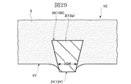
図27は、本発明の実施形態3であるQFN型半導体装置の樹脂封止体の上部を除去した状態を示す模式的平面図、
図28は、図27のI−I線に沿う模式的断面図、
図29は、図28の一部を拡大した模式的断面図、
図30は、本実施形態の半導体装置の製造に用いられるリードフレームの一部を示す模式的平面図、
図31は、図30の各切断線に沿う模式的断面図であり、(a)はJ−J線に沿う模式的断面図、(b)はK−K線に沿う模式的断面図である。
(Embodiment 3)
FIG. 27 is a schematic plan view showing a state in which the upper part of the resin sealing body of the QFN type semiconductor device according to the third embodiment of the present invention is removed;
28 is a schematic cross-sectional view taken along the line II of FIG.
29 is a schematic cross-sectional view enlarging a part of FIG. 28,
FIG. 30 is a schematic plan view showing a part of a lead frame used for manufacturing the semiconductor device of this embodiment.
31 is a schematic cross-sectional view taken along each cutting line of FIG. 30, (a) is a schematic cross-sectional view taken along the line JJ, and (b) is a schematic cross-sectional view taken along the line KK. .
図27乃至図29に示すように、本実施形態のQFN型半導体装置1Cは、基本的に前述の実施形態1と同様の構成になっており、以下の構成が異なっている。 As shown in FIGS. 27 to 29, the QFN type semiconductor device 1C of the present embodiment has basically the same configuration as that of the first embodiment described above, and the following configurations are different.
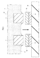
即ち、電極部材3は、一主面3Xの幅よりも裏面3Yの幅の方が狭い楔(くさび)型の断面形状(電極部材3の延在方向と直行する方向の面で切った断面形状)になっている。更に、電極部材3の断面において、樹脂封止体5の裏面5Yと同一の平面に位置する部分での幅3QWよりも裏面3Yの幅の方が狭くなっている。
That is, the
このような電極部材3が樹脂封止体5の裏面5Yに配置されたパッケージ構造は、例えば図30及び図31に示すリードフレーム10Bを用いることで容易に形成することができる。
Such a package structure in which the
リードフレーム10Bにおいて、リード13の電極部分13aは、全体的に、主面13Xの幅13XW1よりも裏面13Yの幅13YW1の方が狭い楔型の断面形状になっている。リード13の電極部分13bも同様に、全体的に、主面13Xの幅13XW2よりも裏面13Yの幅13YW2の方が狭い楔型の断面形状になっている。
In the lead frame 10B, the
このように、電極部材3は、樹脂封止体5の裏面5Yと同一の平面に位置する部分での幅3QWよりも裏面3Yの幅の方が狭い楔型の断面形状になっていることから、ボンディングエリアを確保したうえで、しわの発生を抑制することができる。また、上下面の寸法が同一の時と比較し、リードの剛性がほとんど変わらないため、成形金型でクランプした時にリードの先端部(パッケージ中央方向)が浮き上がらず、フラッシュバリを抑制できる。
As described above, the
(実施形態4)
図32は、本発明の実施形態4であるQFN型半導体装置の模式的底面図、
図33は、図32のL−L線に沿う模式的断面図、
図34は、図33の一部を拡大した模式的断面図、
図35は、本実施形態の半導体装置の製造における樹脂封止工程において、成形金型にリードフレームを位置決めした状態を示す模式的断面図、
図36は、本実施形態の半導体装置を実装基板に実装した状態を示す模式的断面図である。
(Embodiment 4)
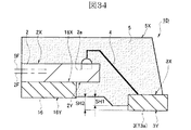
FIG. 32 is a schematic bottom view of a QFN type semiconductor device that is Embodiment 4 of the present invention;
33 is a schematic cross-sectional view taken along line LL of FIG.
34 is a schematic cross-sectional view enlarging a part of FIG.
FIG. 35 is a schematic cross-sectional view showing a state in which the lead frame is positioned in the molding die in the resin sealing step in the manufacture of the semiconductor device of the present embodiment.
FIG. 36 is a schematic cross-sectional view showing a state where the semiconductor device of this embodiment is mounted on a mounting substrate.
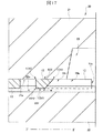
図32乃至図34に示すように、本実施形態のQFN型半導体装置1Dは、基本的に前述の実施形態1と同様の構成になっており、以下の構成が異なっている。
As shown in FIGS. 32 to 34, the QFN
即ち、本実施形態のQFN型半導体装置1Dは、樹脂封止体5の裏面5Yにこの裏面5Yから主面5X側に窪む凹部6を有する構成になっており、更に、凹部6の底面からダイパッド16の裏面16Yが露出する構成になっている。
That is, the QFN
複数の電極部材3は樹脂封止体5の外周囲に沿って配置され、複数の電極部材3の夫々の裏面3Yは樹脂封止体5の裏面5Yよりも突出している。凹部6は複数の電極部材5で囲まれた領域内に複数の電極部材3から離間して設けられている。即ち、本実施形態の半導体装置1Dは、樹脂封止体5の裏面5Y側において、複数のリード3で囲まれた領域に、電極部材3の裏面3Yから凹部6の底面までの段差であって、電極部材3の裏面3Yから樹脂封止体5の裏面5Yまでの段差SH1よりも大きい段差SH2を有する構成になっている。
The plurality of
このように、樹脂封止体5の裏面5Y側に、電極部材3の裏面3Yから樹脂封止体5の裏面5Yまでの段差SH1よりも大きい段差SH2を有するパッケージ構造にすることにより、実装基板の実装面上にQFN型半導体装置1Dを実装する時、実装基板と樹脂封止体5との間に介在された異物に対するマージンがあがるため、異物による電極部材3の浮き不良を低減することができる。この結果、QFN型半導体装置1Dの実装性を向上することができる。
As described above, the packaging substrate has a stepped structure SH2 larger than the stepped SH1 from the
半導体チップ2の厚さ方向の中心2Fが樹脂封止体5の厚さ方向の中心5Fよりも樹脂封止体5の裏面5Y側に位置するパッケージ構造や、樹脂封止体5の裏面5Y側からダイパッド16が露出するパッケージ構造の場合、半導体チップ2の主面2Xより上部にある樹脂の体積よりも半導体チップ2の裏面2Yより下部にある樹脂の体積が小さくなり、樹脂の効果収縮に伴う内部応力のバランスがパッケージの上下で崩れて、樹脂封止体5の裏面5Yが凸となる方向に樹脂封止体5が反る。このような反りが発生したQFN型半導体装置においては、実装基板の実装面と樹脂封止体の裏面の中央部との間隔が最も狭くなるため、例えば実装基板上に形成された凹凸や不意なパーティカルの存在などによって、電極部材3の浮き不良が発生し易くなる。しかしながら、本実施形態のように、電極部材3で囲まれた領域に、電極部材3の裏面3Yから樹脂封止体5の裏面5Yまでの段差SH1よりも大きい段差SH2を有するパッケージ構造にすることにより、樹脂封止体5の反りに起因して最も狭くなる実装基板の実装面と樹脂封止体の裏面の中央部との間隔を確保することができるため、樹脂封止体5の反りによる電極部材3の浮き不良を低減することができる。この結果、QFN型半導体装置1Dの実装性を向上することができる。
A package structure in which the
図36に示すように、実装基板50の実装面には配線53と、この配線53の一部からなる電極51が設けられ、更に、配線53を覆うようにして絶縁膜54が設けられている。QFN型半導体装置1Dの電極部材3は、半田材55によって実装基板50の電極51に固着されている。配線53が絶縁膜54で覆われた部分では、配線53の厚さ分、絶縁膜53が突出する。このような突出部分が樹脂封止体5の裏面5Y下に存在し、しかも突出量が段差SH1よりも大きい場合、電極部材3の浮き不良が発生し易くなる。しかしながら、本実施形態のように、電極部材3で囲まれた領域に、電極部材3の裏面3Yから樹脂封止体5の裏面5Yまでの段差SH1よりも大きい段差SH2を有するパッケージ構造にすることにより、配線53及び絶縁膜54からなる突出部分の高さを段差SH2で吸収できるため、配線53及び絶縁膜54からなる突出部分に起因する電極部材3の浮き不良を低減することができる。この結果、QFN型半導体装置1Dの実装性を向上することができる。
As shown in FIG. 36, the mounting surface of the mounting
このようなQFN型半導体装置1Dは、樹脂封止工程において、図35に示す成形金型20Aを用いることによって容易に形成することができる。成形金型20Aは、基本的に前述の実施形態1の成形金型20と同様の構成になっているが、以下の構成が異なっている。即ち、本実施形態の成形金型20Aは、キャビティ23と向かい合う位置に配置され、かつ下型22の合わせ面22aからキャビティ23側に突出する凸部24を有する構成になっている。
Such a QFN
この成形金型20Aを用いた樹脂封止体5の形成は、まず、ワイヤーボンディング装置からトランスファ・モールディング装置にリードフレーム10を搬送し、図35に示すように、成形金型20Aの上型21と下型22との間にリードフレーム10を位置決めする。リードフレーム10の位置決めは、前述の実施形態1と同様の条件で行われる。次に、このままの状態で、成形金型20Aのポットからカル部、ランナー及び樹脂注入ゲートを通してキャビティ23の内部に例えば熱硬化性の樹脂を加圧注入し、その後、樹脂を硬化させることによって行われる。
In forming the
この樹脂封止工程において、下型22の凸部24上に位置する樹脂シート30にダイパッド16の裏面16Yを接触させた状態で行うことにより、樹脂封止体5の凹部6の底面からダイパッド16の裏面16Yが露出するパッケージ構造が得られる。また、下型22の凸部24上に位置する樹脂シート30からダイパッド16の裏面16Yを離間させた状態で行うことにより、樹脂封止体5の凹部6の底面からダイパッド16の裏面16Yが露出しないパッケージ構造が得られる。
In this resin sealing step, the
段差SH1は、樹脂シート30にリード13が食い込む食い込み量によって調整できる。段差SH2は、下型22の凸部24の突出量によって調整できる。
The level difference SH1 can be adjusted by the amount of biting of the
以上、本発明者によってなされた発明を、前記実施形態に基づき具体的に説明したが、本発明は、前記実施形態に限定されるものではなく、その要旨を逸脱しない範囲において種々変更可能であることは勿論である。 As mentioned above, the invention made by the present inventor has been specifically described based on the embodiment. However, the invention is not limited to the embodiment, and various modifications can be made without departing from the scope of the invention. Of course.
1A,1B,1C,1D,1E…半導体装置
2…半導体チップ
2a…電極
3…電極部材(リードの第1部分)
4…ボンディングワイヤ
5…樹脂封止体
6…凹部
10…リードフレーム
11…フレーム本体
12…製品形成領域
13…リード
13a…リードの電極部分
13b…リードの除去部分
14a…第1リード間領域
14b…第2リード間領域
15…タイバー
16…ダイパッド
17…吊りリード
18…モールドライン
19…切断ライン
20…成形金型
21…上型
22…下型
21a,22a…合わせ面
23…キャビティ
24…凸部
30…樹脂シート(樹脂フィルム)
31…導電層
1A, 1B, 1C, 1D, 1E ...
DESCRIPTION OF SYMBOLS 4 ...
31 ... Conductive layer
Claims (4)
互いに反対側の主面及び裏面を有する電極部材と、
前記半導体チップの電極と前記電極部材の主面とを電気的に接続する接続手段と、
互いに反対側の主面及び裏面を有し、前記半導体チップ、前記電極部材及び前記接続手段を封止する樹脂封止体と、
前記樹脂封止体の裏面から前記樹脂封止体の主面側に向かって窪む凹部とを有し、
前記電極部材の裏面は、前記樹脂封止体の裏面から突出し、
前記凹部の底面から前記電極部材の裏面までの段差は、前記樹脂封止体の裏面から前記電極部材の裏面までの段差よりも大きいことを特徴とする半導体装置。 A semiconductor chip having one main surface;
An electrode member having a main surface and a back surface opposite to each other;
Connection means for electrically connecting the electrode of the semiconductor chip and the main surface of the electrode member;
A resin sealing body having a main surface and a back surface opposite to each other, and sealing the semiconductor chip, the electrode member, and the connection means;
Having a recess recessed from the back surface of the resin sealant toward the main surface of the resin sealant,
The back surface of the electrode member protrudes from the back surface of the resin sealing body,
The semiconductor device according to claim 1, wherein a step from the bottom surface of the recess to the back surface of the electrode member is larger than a step from the back surface of the resin sealing body to the back surface of the electrode member.
前記樹脂封止体は、前記樹脂封止体の裏面が凸面となる方向に反っていることを特徴とする半導体装置。 The semiconductor device according to claim 1,
The semiconductor device is characterized in that the resin sealing body is warped in a direction in which the back surface of the resin sealing body becomes a convex surface.
前記半導体チップは、前記樹脂封止体の主面側に位置する主面と、前記樹脂封止体の裏面側に位置する裏面とを有し、
前記半導体チップの厚さ方向の中心は、前記樹脂封止体の厚さ方向の中心よりも前記樹脂封止体の裏面側に位置していることを特徴とする半導体装置。 The semiconductor device according to claim 1,
The semiconductor chip has a main surface located on the main surface side of the resin sealing body, and a back surface located on the back surface side of the resin sealing body,
The center of the semiconductor chip in the thickness direction is located closer to the back surface side of the resin sealing body than the center of the resin sealing body in the thickness direction.
前記半導体チップが接着固定されたダイパッドを更に有し、
前記ダイパッドは、前記凹部の底面から露出していることを特徴とする半導体装置。 The semiconductor device according to claim 1,
A die pad to which the semiconductor chip is bonded and fixed;
The semiconductor device, wherein the die pad is exposed from the bottom surface of the recess.
Priority Applications (1)
| Application Number | Priority Date | Filing Date | Title |
|---|---|---|---|
| JP2006085030A JP2006210941A (en) | 2006-03-27 | 2006-03-27 | Semiconductor device |
Applications Claiming Priority (1)
| Application Number | Priority Date | Filing Date | Title |
|---|---|---|---|
| JP2006085030A JP2006210941A (en) | 2006-03-27 | 2006-03-27 | Semiconductor device |
Related Parent Applications (1)
| Application Number | Title | Priority Date | Filing Date |
|---|---|---|---|
| JP2001360534A Division JP3798303B2 (en) | 2001-11-27 | 2001-11-27 | Semiconductor device and manufacturing method thereof |
Publications (1)
| Publication Number | Publication Date |
|---|---|
| JP2006210941A true JP2006210941A (en) | 2006-08-10 |
Family
ID=36967343
Family Applications (1)
| Application Number | Title | Priority Date | Filing Date |
|---|---|---|---|
| JP2006085030A Pending JP2006210941A (en) | 2006-03-27 | 2006-03-27 | Semiconductor device |
Country Status (1)
| Country | Link |
|---|---|
| JP (1) | JP2006210941A (en) |
Cited By (4)
| Publication number | Priority date | Publication date | Assignee | Title |
|---|---|---|---|---|
| JP2016105524A (en) * | 2016-03-10 | 2016-06-09 | 大日本印刷株式会社 | Lead frame and method of manufacturing lead frame |
| JP2017085049A (en) * | 2015-10-30 | 2017-05-18 | 新光電気工業株式会社 | Semiconductor device and method of manufacturing the same, lead frame and method of manufacturing the same |
| JP2017123479A (en) * | 2017-03-07 | 2017-07-13 | 大日本印刷株式会社 | Lead frame and method of manufacturing lead frame |
| WO2022153501A1 (en) * | 2021-01-15 | 2022-07-21 | 三菱電機株式会社 | Semiconductor device, method for producing same and semiconductor package |
Citations (7)
| Publication number | Priority date | Publication date | Assignee | Title |
|---|---|---|---|---|
| JPH0369248U (en) * | 1989-11-10 | 1991-07-09 | ||
| JPH0778921A (en) * | 1993-09-09 | 1995-03-20 | Shinko Electric Ind Co Ltd | Semiconductor device |
| JPH113953A (en) * | 1997-06-10 | 1999-01-06 | Fujitsu Ltd | Semiconductor device and manufacture thereof |
| JP2000150723A (en) * | 1998-11-16 | 2000-05-30 | Hitachi Ltd | Semiconductor device and its manufacture |
| JP2001035961A (en) * | 1999-07-21 | 2001-02-09 | Sony Corp | Semiconductor and manufacture thereof |
| JP2001077266A (en) * | 1999-09-01 | 2001-03-23 | Matsushita Electronics Industry Corp | Manufacture of resin sealed semiconductor device |
| JP2001185567A (en) * | 1999-12-22 | 2001-07-06 | Hitachi Ltd | Semiconductor device and manufacturing method therefor |
-
2006
- 2006-03-27 JP JP2006085030A patent/JP2006210941A/en active Pending
Patent Citations (7)
| Publication number | Priority date | Publication date | Assignee | Title |
|---|---|---|---|---|
| JPH0369248U (en) * | 1989-11-10 | 1991-07-09 | ||
| JPH0778921A (en) * | 1993-09-09 | 1995-03-20 | Shinko Electric Ind Co Ltd | Semiconductor device |
| JPH113953A (en) * | 1997-06-10 | 1999-01-06 | Fujitsu Ltd | Semiconductor device and manufacture thereof |
| JP2000150723A (en) * | 1998-11-16 | 2000-05-30 | Hitachi Ltd | Semiconductor device and its manufacture |
| JP2001035961A (en) * | 1999-07-21 | 2001-02-09 | Sony Corp | Semiconductor and manufacture thereof |
| JP2001077266A (en) * | 1999-09-01 | 2001-03-23 | Matsushita Electronics Industry Corp | Manufacture of resin sealed semiconductor device |
| JP2001185567A (en) * | 1999-12-22 | 2001-07-06 | Hitachi Ltd | Semiconductor device and manufacturing method therefor |
Cited By (4)
| Publication number | Priority date | Publication date | Assignee | Title |
|---|---|---|---|---|
| JP2017085049A (en) * | 2015-10-30 | 2017-05-18 | 新光電気工業株式会社 | Semiconductor device and method of manufacturing the same, lead frame and method of manufacturing the same |
| JP2016105524A (en) * | 2016-03-10 | 2016-06-09 | 大日本印刷株式会社 | Lead frame and method of manufacturing lead frame |
| JP2017123479A (en) * | 2017-03-07 | 2017-07-13 | 大日本印刷株式会社 | Lead frame and method of manufacturing lead frame |
| WO2022153501A1 (en) * | 2021-01-15 | 2022-07-21 | 三菱電機株式会社 | Semiconductor device, method for producing same and semiconductor package |
Similar Documents
| Publication | Publication Date | Title |
|---|---|---|
| US7514293B2 (en) | Method of manufacturing a semiconductor device | |
| US7638879B2 (en) | Semiconductor package and fabrication method thereof | |
| US9385072B2 (en) | Method of manufacturing semiconductor device and semiconductor device | |
| JP5122835B2 (en) | Semiconductor device, lead frame, and manufacturing method of semiconductor device | |
| US8133759B2 (en) | Leadframe | |
| JP2005191240A (en) | Semiconductor device and method for manufacturing the same | |
| JP2014007363A (en) | Method of manufacturing semiconductor device and semiconductor device | |
| JP6357371B2 (en) | Lead frame, semiconductor device, and lead frame manufacturing method | |
| KR20000048011A (en) | A semiconductor device | |
| JP2000307045A (en) | Lead frame and manufacture of resin sealed semiconductor device using it | |
| US9331041B2 (en) | Semiconductor device and semiconductor device manufacturing method | |
| JP2005244035A (en) | Mounting method of semiconductor device, and semiconductor device | |
| JP2006210941A (en) | Semiconductor device | |
| JP2006140208A (en) | Resin sealed semiconductor device, lead frame with die pad and manufacturing method of lead frame with die pad | |
| JP2008071927A (en) | Manufacturing method of semiconductor device, and semiconductor device | |
| JP3798303B2 (en) | Semiconductor device and manufacturing method thereof | |
| JP2006279088A (en) | Method for manufacturing semiconductor device | |
| JP5569097B2 (en) | Semiconductor device and lead frame | |
| JP2007134585A (en) | Semiconductor device and its manufacturing method | |
| JP4840305B2 (en) | Manufacturing method of semiconductor device | |
| KR20070103591A (en) | Semiconductor package having insulator interposed between leads and method of fabricating semiconductor device having the same | |
| JP2001077285A (en) | Lead frame and manufacture of resin-sealed semiconductor device using the same | |
| JP4695672B2 (en) | Semiconductor device | |
| JP2017108191A (en) | Semiconductor device | |
| JP2002164496A (en) | Semiconductor device and method for manufacturing the same |
Legal Events
| Date | Code | Title | Description |
|---|---|---|---|
| A977 | Report on retrieval |
Free format text: JAPANESE INTERMEDIATE CODE: A971007 Effective date: 20080616 |
|
| A131 | Notification of reasons for refusal |
Free format text: JAPANESE INTERMEDIATE CODE: A131 Effective date: 20080624 |
|
| A521 | Written amendment |
Free format text: JAPANESE INTERMEDIATE CODE: A523 Effective date: 20080825 |
|
| A131 | Notification of reasons for refusal |
Free format text: JAPANESE INTERMEDIATE CODE: A131 Effective date: 20081104 |
|
| A02 | Decision of refusal |
Free format text: JAPANESE INTERMEDIATE CODE: A02 Effective date: 20090310 |