JP2006142780A - Head substrate, recording head, head cartridge, and recorder using recording head or head cartridge - Google Patents
Head substrate, recording head, head cartridge, and recorder using recording head or head cartridge Download PDFInfo
- Publication number
- JP2006142780A JP2006142780A JP2004339443A JP2004339443A JP2006142780A JP 2006142780 A JP2006142780 A JP 2006142780A JP 2004339443 A JP2004339443 A JP 2004339443A JP 2004339443 A JP2004339443 A JP 2004339443A JP 2006142780 A JP2006142780 A JP 2006142780A
- Authority
- JP
- Japan
- Prior art keywords
- recording
- head
- ink
- heater
- resistance
- Prior art date
- Legal status (The legal status is an assumption and is not a legal conclusion. Google has not performed a legal analysis and makes no representation as to the accuracy of the status listed.)
- Abandoned
Links
Images


Classifications
-
- B—PERFORMING OPERATIONS; TRANSPORTING
- B41—PRINTING; LINING MACHINES; TYPEWRITERS; STAMPS
- B41J—TYPEWRITERS; SELECTIVE PRINTING MECHANISMS, i.e. MECHANISMS PRINTING OTHERWISE THAN FROM A FORME; CORRECTION OF TYPOGRAPHICAL ERRORS
- B41J2/00—Typewriters or selective printing mechanisms characterised by the printing or marking process for which they are designed
- B41J2/005—Typewriters or selective printing mechanisms characterised by the printing or marking process for which they are designed characterised by bringing liquid or particles selectively into contact with a printing material
- B41J2/01—Ink jet
- B41J2/015—Ink jet characterised by the jet generation process
- B41J2/04—Ink jet characterised by the jet generation process generating single droplets or particles on demand
- B41J2/045—Ink jet characterised by the jet generation process generating single droplets or particles on demand by pressure, e.g. electromechanical transducers
- B41J2/04501—Control methods or devices therefor, e.g. driver circuits, control circuits
- B41J2/0451—Control methods or devices therefor, e.g. driver circuits, control circuits for detecting failure, e.g. clogging, malfunctioning actuator
-
- B—PERFORMING OPERATIONS; TRANSPORTING
- B41—PRINTING; LINING MACHINES; TYPEWRITERS; STAMPS
- B41J—TYPEWRITERS; SELECTIVE PRINTING MECHANISMS, i.e. MECHANISMS PRINTING OTHERWISE THAN FROM A FORME; CORRECTION OF TYPOGRAPHICAL ERRORS
- B41J2/00—Typewriters or selective printing mechanisms characterised by the printing or marking process for which they are designed
- B41J2/005—Typewriters or selective printing mechanisms characterised by the printing or marking process for which they are designed characterised by bringing liquid or particles selectively into contact with a printing material
- B41J2/01—Ink jet
- B41J2/015—Ink jet characterised by the jet generation process
- B41J2/04—Ink jet characterised by the jet generation process generating single droplets or particles on demand
- B41J2/045—Ink jet characterised by the jet generation process generating single droplets or particles on demand by pressure, e.g. electromechanical transducers
- B41J2/04501—Control methods or devices therefor, e.g. driver circuits, control circuits
- B41J2/04538—Control methods or devices therefor, e.g. driver circuits, control circuits involving calculation of heater resistance
-
- B—PERFORMING OPERATIONS; TRANSPORTING
- B41—PRINTING; LINING MACHINES; TYPEWRITERS; STAMPS
- B41J—TYPEWRITERS; SELECTIVE PRINTING MECHANISMS, i.e. MECHANISMS PRINTING OTHERWISE THAN FROM A FORME; CORRECTION OF TYPOGRAPHICAL ERRORS
- B41J2/00—Typewriters or selective printing mechanisms characterised by the printing or marking process for which they are designed
- B41J2/005—Typewriters or selective printing mechanisms characterised by the printing or marking process for which they are designed characterised by bringing liquid or particles selectively into contact with a printing material
- B41J2/01—Ink jet
- B41J2/015—Ink jet characterised by the jet generation process
- B41J2/04—Ink jet characterised by the jet generation process generating single droplets or particles on demand
- B41J2/045—Ink jet characterised by the jet generation process generating single droplets or particles on demand by pressure, e.g. electromechanical transducers
- B41J2/04501—Control methods or devices therefor, e.g. driver circuits, control circuits
- B41J2/04541—Specific driving circuit
-
- B—PERFORMING OPERATIONS; TRANSPORTING
- B41—PRINTING; LINING MACHINES; TYPEWRITERS; STAMPS
- B41J—TYPEWRITERS; SELECTIVE PRINTING MECHANISMS, i.e. MECHANISMS PRINTING OTHERWISE THAN FROM A FORME; CORRECTION OF TYPOGRAPHICAL ERRORS
- B41J2/00—Typewriters or selective printing mechanisms characterised by the printing or marking process for which they are designed
- B41J2/005—Typewriters or selective printing mechanisms characterised by the printing or marking process for which they are designed characterised by bringing liquid or particles selectively into contact with a printing material
- B41J2/01—Ink jet
- B41J2/015—Ink jet characterised by the jet generation process
- B41J2/04—Ink jet characterised by the jet generation process generating single droplets or particles on demand
- B41J2/045—Ink jet characterised by the jet generation process generating single droplets or particles on demand by pressure, e.g. electromechanical transducers
- B41J2/04501—Control methods or devices therefor, e.g. driver circuits, control circuits
- B41J2/04553—Control methods or devices therefor, e.g. driver circuits, control circuits detecting ambient temperature
-
- B—PERFORMING OPERATIONS; TRANSPORTING
- B41—PRINTING; LINING MACHINES; TYPEWRITERS; STAMPS
- B41J—TYPEWRITERS; SELECTIVE PRINTING MECHANISMS, i.e. MECHANISMS PRINTING OTHERWISE THAN FROM A FORME; CORRECTION OF TYPOGRAPHICAL ERRORS
- B41J2/00—Typewriters or selective printing mechanisms characterised by the printing or marking process for which they are designed
- B41J2/005—Typewriters or selective printing mechanisms characterised by the printing or marking process for which they are designed characterised by bringing liquid or particles selectively into contact with a printing material
- B41J2/01—Ink jet
- B41J2/015—Ink jet characterised by the jet generation process
- B41J2/04—Ink jet characterised by the jet generation process generating single droplets or particles on demand
- B41J2/045—Ink jet characterised by the jet generation process generating single droplets or particles on demand by pressure, e.g. electromechanical transducers
- B41J2/04501—Control methods or devices therefor, e.g. driver circuits, control circuits
- B41J2/04565—Control methods or devices therefor, e.g. driver circuits, control circuits detecting heater resistance
-
- B—PERFORMING OPERATIONS; TRANSPORTING
- B41—PRINTING; LINING MACHINES; TYPEWRITERS; STAMPS
- B41J—TYPEWRITERS; SELECTIVE PRINTING MECHANISMS, i.e. MECHANISMS PRINTING OTHERWISE THAN FROM A FORME; CORRECTION OF TYPOGRAPHICAL ERRORS
- B41J2/00—Typewriters or selective printing mechanisms characterised by the printing or marking process for which they are designed
- B41J2/005—Typewriters or selective printing mechanisms characterised by the printing or marking process for which they are designed characterised by bringing liquid or particles selectively into contact with a printing material
- B41J2/01—Ink jet
- B41J2/015—Ink jet characterised by the jet generation process
- B41J2/04—Ink jet characterised by the jet generation process generating single droplets or particles on demand
- B41J2/045—Ink jet characterised by the jet generation process generating single droplets or particles on demand by pressure, e.g. electromechanical transducers
- B41J2/04501—Control methods or devices therefor, e.g. driver circuits, control circuits
- B41J2/0458—Control methods or devices therefor, e.g. driver circuits, control circuits controlling heads based on heating elements forming bubbles
Abstract
Description
本発明はヘッド基板、記録ヘッド、ヘッドカートリッジ、及びその記録ヘッド或いはヘッドカートリッジを用いた記録装置に関し、特に、例えば、インクを吐出するために必要な熱エネルギーを発生する電気熱変換素子とそれを駆動するための駆動回路を同一の基板上に形成したヘッド基板、そのヘッド基板を用いた記録ヘッド、その記録ヘッドを用いたヘッドカートリッジ、及びその記録ヘッド或いはヘッドカートリッジを用いた記録装置に関する。 The present invention relates to a head substrate, a recording head, a head cartridge, and a recording apparatus using the recording head or the head cartridge, and more particularly, for example, an electrothermal conversion element that generates thermal energy necessary for ejecting ink and the same. The present invention relates to a head substrate having a driving circuit for driving on the same substrate, a recording head using the head substrate, a head cartridge using the recording head, and a recording apparatus using the recording head or head cartridge.
従来よりワードプロセッサ、パーソナルコンピュータ、ファクシミリ等に用いられるおける情報出力装置として、所望される文字や画像等を記録用紙やフィルム等のシート状の記録媒体に行うプリンタが知られている。 2. Description of the Related Art Conventionally, as information output devices used in word processors, personal computers, facsimiles, and the like, printers that perform desired characters and images on a sheet-like recording medium such as recording paper or film are known.
プリンタの記録方式としては様々な方式が知られているが中でも、記録媒体に対して非接触で記録が可能であり、カラー記録が容易であり、静粛性に富む等の利点があることからインクジェット方式が特に注目されている。 Various types of printer recording methods are known. Among them, inkjet printing is possible due to the advantages of non-contact recording on recording media, easy color recording, and high quietness. The method is attracting particular attention.
特に、ヒータに数μ秒程度通電することで発生する熱エネルギーにより誘発されるインクの発泡現象をインク液滴の吐出に利用するサーマルインクジェット方式は、高密度に多数のノズルを記録ヘッドに形成することが可能である。 In particular, the thermal ink jet method that utilizes the ink bubbling phenomenon induced by the thermal energy generated by energizing the heater for several microseconds to eject ink droplets forms a large number of nozzles at a high density on the recording head. It is possible.
このようなサーマルインクジェット方式の記録ヘッド(以下、記録ヘッド)では、シリコン単結晶基板などに半導体集積回路プロセスによりインクを加熱するヒータとその保護膜、およびヒータに電流を流すためのドライバ回路とその制御を行う論理回路などを一体で形成した記録素子(以下、ヒータボード)を用いている。 In such a thermal ink jet recording head (hereinafter referred to as a recording head), a heater for heating ink on a silicon single crystal substrate or the like by a semiconductor integrated circuit process, its protective film, and a driver circuit for supplying current to the heater and its A recording element (hereinafter referred to as a heater board) in which a logic circuit for performing control is integrally formed is used.
図9は従来より一般的に知られているヒータボード内部のヒータとその駆動回路の回路構成を示す図である。 FIG. 9 is a diagram showing a circuit configuration of a heater inside a heater board and a drive circuit thereof generally known conventionally.
図9において、101はインクの加熱を行うためのヒータ、102はヒータへの電流印加のスイッチとなるドライバトランジスタ、103〜104はヒータ101及びドライバトランジスタ102を記録ヘッド外部との電気的接続を行うためのパッドへと引き出すための配線に寄生する配線抵抗、105〜106はそれぞれ外部から電源を印加するためのパッド端子VH(正電位)およびGNDH(基準電位)である。
In FIG. 9, 101 is a heater for heating the ink, 102 is a driver transistor that serves as a switch for applying a current to the heater, and 103 to 104 electrically connect the
図9から明らかなように、ヒータ101とドライバトランジスタ102は1対1の関係になっており、任意のドライバトランジスタを選択駆動することで、対応するヒータへの電流の通電制御が可能となる。ここで、ドライバトランジスタの選択駆動は、ヒータボード内部回路(不図示)から出力される素子選択出力がドライバトランジスタのゲート端子107に加えられることにより行われる。
As is apparent from FIG. 9, the
さて、パッドからヒータ、ドライバトランジスタへの電気的接続は、図9にも示されているように、複数の隣接したヒータとドライバトランジスタを一つのまとまりとして、それぞれのまとまりに対して独立した配線で行われている。これは各々のヒータ、ドライバトランジスタとパッド間の距離による抵抗値のズレを、一定の範囲内となるようにするためであり、かつ各々のまとまりの中で同時に通電するヒータを一つに限定することで、配線抵抗での電圧降下を、各々のまとまりの間で一定なものとするためである。 As shown in FIG. 9, the electrical connection from the pad to the heater and the driver transistor is made up of a plurality of adjacent heaters and driver transistors as one unit, and independent wiring for each unit. Has been done. This is to make the deviation of the resistance value due to the distance between each heater, driver transistor and pad to be within a certain range, and to limit the number of heaters energized simultaneously in each unit to one. This is to make the voltage drop at the wiring resistance constant between each unit.
このようにヒータボード上に多数形成したヒータは、理想的には全てのヒータで均一なばらつきのないパワーを発生できることが望まれるが、実際にはばらつきが存在する。 The heaters formed in large numbers on the heater board as described above are ideally capable of generating uniform power without any variation in all the heaters, but there are actually variations.
このばらつきとしては、ヒータとヒータボード上の電気接点となるパッドとを接続する配線抵抗、およびヒータへの通電制御を行うドライバトランジスタのオン抵抗、及びヒータの抵抗値ばらつきなどにより生じるものである。 This variation is caused by a wiring resistance that connects the heater and a pad that serves as an electrical contact on the heater board, an ON resistance of a driver transistor that controls energization of the heater, a variation in the resistance value of the heater, and the like.
ヒータで発生するパワー(電力)のばらつきは、ヒータの抵抗値ではないばらつき、即ち、配線抵抗やドライバトランジスタのオン抵抗のばらつきに対しては直接的に影響を受ける。即ち、ヒータ以外の抵抗が高くなると、その高くなった抵抗で電圧および電流が消費されることとなり、ヒータで発生するパワーが減少するのである。 The variation in power (electric power) generated in the heater is directly affected by the variation other than the resistance value of the heater, that is, the variation in the wiring resistance and the ON resistance of the driver transistor. That is, when the resistance other than the heater is increased, voltage and current are consumed by the increased resistance, and the power generated in the heater is reduced.
一方、ヒータ抵抗のばらつきは、パワーのばらつきに対しては圧縮されて影響する。 On the other hand, the variation in heater resistance is compressed and affects the variation in power.
即ち、ヒータ抵抗のばらつきにより、個々のヒータ抵抗が設計中心値よりも高いものとなった場合、そのヒータに印加される電圧は大きくなる一方、流れる電流は小さくなる。しかしながら、発生電力は電圧と電流の積として表現されるので、結果としては電圧と電流の増減が相殺され、ヒータ以外の抵抗がばらついた場合に比較して小さい影響となる。 That is, when the individual heater resistance becomes higher than the design center value due to variations in the heater resistance, the voltage applied to the heater increases while the flowing current decreases. However, since the generated power is expressed as a product of voltage and current, the increase and decrease in voltage and current are offset as a result, and the influence is small compared to the case where resistance other than the heater varies.
図10は1つのヒータに電流を流す回路構成を模式的に示す図である。 FIG. 10 is a diagram schematically showing a circuit configuration in which a current flows through one heater.
図10において、Rhはヒータ101の抵抗、Rpがヒータ以外の配線抵抗およびトランジスタのオン抵抗などの寄生抵抗108の合計である。これらの抵抗は直列に接続されているものである。
In FIG. 10, Rh is the resistance of the
ここで、設計中心値として、ヒータ抵抗をRh=100Ω、配線およびオン抵抗のなどからなる寄生抵抗をRp=50Ω、端子間の電源電圧(V)をV=15Vと仮定する。 Here, as the design center value, it is assumed that the heater resistance is Rh = 100Ω, the parasitic resistance composed of wiring and on-resistance is Rp = 50Ω, and the power supply voltage (V) between terminals is V = 15V.
この条件で、ヒータで発生するパワーは、系としての合計抵抗が100Ω+50Ω=150Ω、端子間の電圧が15Vであることから電流(I)は、
I=V/R=15V/150Ω=0.1A であるため、
V×I=R×I2=100Ω×(0.1A)2=1Wとなる。
Under this condition, the power generated in the heater is such that the total resistance as a system is 100Ω + 50Ω = 150Ω, and the voltage between the terminals is 15V, so the current (I) is
Since I = V / R = 15V / 150Ω = 0.1A,
V × I = R × I 2 = 100Ω × (0.1 A) 2 = 1W.
ここで、寄生抵抗が中心値の50Ωから60Ωにばらついたと仮定すると、ヒータで発生するパワーは、
系としての合計抵抗が100Ω+60Ω=160Ω、端子間の電圧が15Vであることから、
I=V/R=15V/160Ω=0.0938Aであるため、
発生するパワーは、
P=V×I=R×I2=100Ω×(0.0938A)2=0.880Wとなる。
Here, assuming that the parasitic resistance varies from the central value of 50Ω to 60Ω, the power generated in the heater is
Since the total resistance as a system is 100Ω + 60Ω = 160Ω and the voltage between terminals is 15V,
Since I = V / R = 15V / 160Ω = 0.0938A,
The generated power is
P = V × I = R × I 2 = 100Ω × (0.0938A) 2 = 0.880W.
一方、寄生抵抗は中心値50Ωのままで、ヒータの抵抗値が中心値の100Ωから110Ωにばらついたと仮定すると、系としての合計抵抗は先ほどと同様の100Ω+60Ω=160Ω、端子間の電圧が15Vであることから、
I=V/R=15V/160Ω=0.0938A である。
On the other hand, assuming that the parasitic resistance remains at the central value of 50Ω and the resistance value of the heater varies from the central value of 100Ω to 110Ω, the total resistance as the system is 100Ω + 60Ω = 160Ω, and the voltage between the terminals is 15V. Because there is
I = V / R = 15V / 160Ω = 0.0938A
しかしながら、ヒータで発生するパワーは、
P=V×I=R×I2=110Ω×(0.0938A)2=0.968Wとなる。従って、ヒータ抵抗の高い値へのばらつきは寄生抵抗のばらつきよりもパワーのばらつきに対する影響は小さいものとなる。同様に、ヒータ抵抗の低い値へのばらつきも、寄生抵抗のばらつきよりパワーのばらつきに対する影響は小さい。
However, the power generated by the heater is
P = V × I = R × I 2 = 110Ω × (0.0938A) 2 = 0.968W. Therefore, the variation of the heater resistance to a higher value has a smaller influence on the variation of power than the variation of parasitic resistance. Similarly, the variation of the heater resistance to a low value has less influence on the variation of power than the variation of parasitic resistance.
以上説明したように、ヒータボードに形成された記録要素であるヒータ抵抗、及び配線や駆動トランジスタのオン抵抗などの寄生抵抗は、その抵抗値にばらつきがある。 As described above, the resistance values of the heater resistance, which is a recording element formed on the heater board, and the parasitic resistance such as the on-resistance of the wiring and the driving transistor vary.
そして、これら抵抗値のばらつきは、許容範囲であるかどうかを電気的に測定することによって判断される。従来、このような測定はヒータ抵抗および寄生抵抗の合計抵抗を測定することにより行われている。 These variations in resistance value are determined by electrically measuring whether or not the resistance value is within an allowable range. Conventionally, such measurement is performed by measuring the total resistance of the heater resistance and the parasitic resistance.
上記の説明から明らかなように、抵抗値ばらつきの要因がヒータ抵抗であるのか、寄生抵抗であるのかによってヒータで発生するパワーのばらつきは異なったものとなる。
さて、記録ヘッドの安定的な動作確認という観点から見ると、本来必要な情報はヒータで発生するパワーのばらつきであるが、従来ではそのばらつき測定をヒータ抵抗と寄生抵抗との合計抵抗を測定していたため、ばらつき要因がヒータ抵抗であるのか、寄生抵抗であるのかの分離が困難であった。上記の検討からも明らかなように、このばらつき要因がヒータ抵抗による場合には、寄生抵抗による場合よりも許容範囲を広くすることが可能である。 From the viewpoint of confirming the stable operation of the recording head, the essential information is the variation in power generated by the heater. Conventionally, this variation is measured by measuring the total resistance of the heater resistance and parasitic resistance. Therefore, it is difficult to separate whether the variation factor is a heater resistance or a parasitic resistance. As apparent from the above examination, when the variation factor is due to the heater resistance, the allowable range can be made wider than that due to the parasitic resistance.
しかしながら上記従来例では、これらの要因の分離が困難であったので、常に最悪の事態を想定する必要があり、測定により得られたばらつきが全て寄生抵抗からの寄与によるものであった場合においても問題がないようにその規格を規定する必要があった。そのため、本来ヒータで発生するパワーが製品としての規格を満たすものであったとしても、系全体としての合計の抵抗値がその規格を満足しない場合においては、そのヒータボードを不良として判定することとなり、これが歩留まりを低下させる要因となっていた。 However, in the above conventional example, it is difficult to separate these factors, so it is necessary to always assume the worst situation, and even when the variation obtained by the measurement is all due to the contribution from the parasitic resistance. It was necessary to define the standard so that there was no problem. Therefore, even if the power generated by the heater originally satisfies the product standard, if the total resistance value of the entire system does not satisfy the standard, the heater board is determined to be defective. This was a factor that reduced the yield.
本発明は上記問題点に鑑みてなされたもので、記録素子の抵抗のばらつきと、配線抵抗および駆動素子のオン抵抗などからなる寄生抵抗のばらつきとを分離して測定可能なヘッド基板、記録ヘッド、ヘッドカートリッジ、及びその記録ヘッド或いはヘッドカートリッジを用いた記録装置を提供することを目的としている。 The present invention has been made in view of the above problems, and a head substrate and a recording head capable of separately measuring variations in resistance of recording elements and variations in parasitic resistance including wiring resistance and on-resistance of driving elements. It is an object of the present invention to provide a head cartridge and a recording apparatus using the recording head or the head cartridge.
上記目的を達成するために本発明のヘッド基板は、以下のような構成からなる。 In order to achieve the above object, the head substrate of the present invention has the following configuration.
即ち、複数の記録素子と前記複数の記録素子を駆動する複数の駆動素子とを備えたヘッド基板であって、前記複数の記録素子にテスト信号を入力する第1の端子と、前記複数の記録素子の少なくとも一部の記録素子に関し、該記録素子を選択駆動する選択信号を入力する第2の端子と、前記選択信号により選択された記録素子の少なくとも一端の電位を出力する第3の端子とを有することを特徴とする。 That is, a head substrate including a plurality of recording elements and a plurality of driving elements for driving the plurality of recording elements, the first terminal for inputting a test signal to the plurality of recording elements, and the plurality of recording elements A second terminal for inputting a selection signal for selectively driving the recording element, and a third terminal for outputting a potential of at least one end of the recording element selected by the selection signal with respect to at least a part of the recording elements; It is characterized by having.
さらに、前記選択信号により選択された記録素子に関し、もう一方の端の電位を出力する第4の端子を備えると良い。 Furthermore, it is preferable to provide a fourth terminal for outputting the potential at the other end of the recording element selected by the selection signal.
ここで、前記複数の駆動素子は第1のMOSトランジスタであり、前記選択信号により記録素子を選択するための第2のMOSトランジスタと、前記テスト信号により記録素子に通電するための第3のMOSトランジスタとをさらに備えることが望ましい。 Here, the plurality of drive elements are first MOS transistors, a second MOS transistor for selecting a recording element by the selection signal, and a third MOS for energizing the recording element by the test signal. It is desirable to further include a transistor.
この場合、前記選択信号は第1及び第2のMOSトランジスタのゲートに共通入力され、前記テスト信号は第3のMOSトランジスタのゲートに入力されるように構成することが望ましい。 In this case, it is preferable that the selection signal is input in common to the gates of the first and second MOS transistors, and the test signal is input to the gate of the third MOS transistor.
また、前記少なくとも一端の電位とは、前記記録素子が第1のMOSトランジスタに接続される側の電位であり、前記もう一方の端の電位とは、前記記録素子が第1のMOSトランジスタに接続される側とは反対側の前記複数の記録素子に共通の電源が接続される側の電位である。 The potential at at least one end is a potential on the side where the recording element is connected to the first MOS transistor, and the potential at the other end is connected to the first MOS transistor. This is the potential on the side where a common power supply is connected to the plurality of recording elements on the side opposite to the side to be applied.
さらに、前記複数の記録素子に共通の電源を接続する側と前記第4の端子との間に直列に接続される第4及び第5のMOSトランジスタを備え、第4のMOSトランジスタのゲートには前記選択信号が、第5のMOSトランジスタには前記テスト信号が入力されるように構成すると良い。 The fourth MOS transistor further includes fourth and fifth MOS transistors connected in series between a side connecting a common power source to the plurality of recording elements and the fourth terminal. The selection signal may be configured such that the test signal is input to the fifth MOS transistor.
また他の発明に従えば、上記構成のヘッド基板を用いた記録ヘッドを備える。 According to another invention, a recording head using the head substrate having the above structure is provided.
前記記録ヘッドは、インクを吐出して記録を行うインクジェット記録ヘッドでも良く、そのインクジェット記録ヘッドは、熱エネルギーを利用してインクを吐出するために、インクに与える熱エネルギーを発生するための電気熱変換体を備えていることがより好ましい。 The recording head may be an ink jet recording head that performs recording by discharging ink, and the ink jet recording head uses electric energy to generate thermal energy to be applied to the ink in order to discharge ink using thermal energy. More preferably, a converter is provided.
さらに他の発明に従えば、上記構成のインクジェット記録ヘッドとそのインクジェット記録ヘッドにインクを供給するためのインクを貯留するインクタンクとを有することを特徴とするヘッドカートリッジを備える。 According to still another aspect of the invention, there is provided a head cartridge including the ink jet recording head having the above-described configuration and an ink tank for storing ink for supplying ink to the ink jet recording head.
またさらに他の発明に従えば、上記の構成の記録ヘッド或いはヘッドカートリッジを用いて記録を行う記録装置を備える。 According to still another aspect of the invention, a recording apparatus that performs recording using the recording head or the head cartridge having the above-described configuration is provided.
従って本発明によれば、記録素子の少なくとも一端の電圧が端子を通してヘッド基板の外部に出力することができるので、記録素子の例えば抵抗成分とそれ以外の寄生抵抗成分を分離して測定することが可能になるという効果がある。 Therefore, according to the present invention, since the voltage of at least one end of the recording element can be output to the outside of the head substrate through the terminal, for example, the resistance component of the recording element and the other parasitic resistance component can be measured separately. There is an effect that it becomes possible.
これにより、従来の抵抗値測定により実施していたばらつきの許容範囲を記録素子に直接起因するパワーばらつきによる許容範囲とすることが可能となるので、そのばらつきの許容範囲を従来よりも広いものとすることが可能となる。そのため従来の測定方法では不良品となっていたヘッド基板を良品と判定することが可能となり、その製造歩留まりの向上を達成することができる。 As a result, it becomes possible to make the allowable range of variation carried out by the conventional resistance value measurement to be an allowable range due to power variation directly attributable to the recording element, so that the allowable range of variation is wider than before. It becomes possible to do. Therefore, it is possible to determine that the head substrate, which has been a defective product in the conventional measurement method, is a non-defective product, and the manufacturing yield can be improved.
以下添付図面を参照して本発明の好適な実施例について、さらに具体的かつ詳細に説明する。 Hereinafter, preferred embodiments of the present invention will be described more specifically and in detail with reference to the accompanying drawings.
なお、この明細書において、「記録」(「プリント」という場合もある)とは、文字、図形等有意の情報を形成する場合のみならず、有意無意を問わず、また人間が視覚で知覚し得るように顕在化したものであるか否かを問わず、広く記録媒体上に画像、模様、パターン等を形成する、または媒体の加工を行う場合も表すものとする。 In this specification, “recording” (sometimes referred to as “printing”) is not only for forming significant information such as characters and figures, but also for human beings visually perceived regardless of significance. Regardless of whether or not it has been manifested, it also represents a case where an image, a pattern, a pattern, or the like is widely formed on a recording medium or the medium is processed.
また、「記録媒体」とは、一般的な記録装置で用いられる紙のみならず、広く、布、プラスチック・フィルム、金属板、ガラス、セラミックス、木材、皮革等、インクを受容可能なものも表すものとする。 “Recording medium” refers not only to paper used in general recording apparatuses but also widely to cloth, plastic film, metal plate, glass, ceramics, wood, leather, and the like that can accept ink. Shall.
さらに、「インク」(「液体」と言う場合もある)とは、上記「記録(プリント)」の定義と同様広く解釈されるべきもので、記録媒体上に付与されることによって、画像、模様、パターン等の形成または記録媒体の加工、或いはインクの処理(例えば記録媒体に付与されるインク中の色剤の凝固または不溶化)に供され得る液体を表すものとする。 Furthermore, “ink” (sometimes referred to as “liquid”) is to be interpreted broadly in the same way as the definition of “recording (printing)” above. It represents a liquid that can be used for forming a pattern or the like, processing a recording medium, or processing an ink (for example, solidification or insolubilization of a colorant in ink applied to the recording medium).
またさらに、「ノズル」とは、特にことわらない限り吐出口ないしこれに連通する液路およびインク吐出に利用されるエネルギーを発生する素子を総括して言うものとする。 Furthermore, unless otherwise specified, the “nozzle” collectively refers to an ejection port or a liquid channel communicating with the ejection port and an element that generates energy used for ink ejection.
なお、説明で用いる「素子基体上」という表現は、単に素子基体の上を指し示すだけでなく、素子基体の表面、表面近傍の素子基体内部側をも示すものである。また、本発明でいう「作りこみ(ビルトイン(built-in))」とは、別体の各素子を単に基体上に配置することを指し示している言葉ではなく、各素子を半導体回路の製造工程などによって素子基体上に一体的に形成、製造することを示すものである。 The expression “on the element substrate” used in the description not only indicates the element substrate, but also indicates the surface of the element substrate and the inside of the element substrate near the surface. In addition, the term “built-in” as used in the present invention is not a term indicating that individual elements are simply arranged on a substrate, but each element is a manufacturing process of a semiconductor circuit. It shows that it is integrally formed and manufactured on the element substrate by the above.
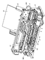
<インクジェット記録装置の説明(図1)>
図1は本発明の代表的な実施例であるインクジェット記録装置1の構成の概要を示す外観斜視図である。
<Description of Inkjet Recording Apparatus (FIG. 1)>
FIG. 1 is an external perspective view showing an outline of the configuration of an ink jet recording apparatus 1 which is a typical embodiment of the present invention.
図1に示すように、インクジェット記録装置(以下、記録装置という)は、インクジェット方式に従ってインクを吐出して記録を行なう記録ヘッド3を搭載したキャリッジ2にキャリッジモータM1によって発生する駆動力を伝達機構4より伝え、キャリッジ2を矢印A方向に往復移動させるとともに、例えば、記録紙などの記録媒体Pを給紙機構5を介して給紙し、記録位置まで搬送し、その記録位置において記録ヘッド3から記録媒体Pにインクを吐出することで記録を行なう。
As shown in FIG. 1, an ink jet recording apparatus (hereinafter referred to as a recording apparatus) transmits a driving force generated by a carriage motor M1 to a
また、記録ヘッド3の状態を良好に維持するためにキャリッジ2を回復装置10の位置まで移動させ、間欠的に記録ヘッド3の吐出回復処理を行う。
Further, in order to maintain the state of the
記録装置1のキャリッジ2には記録ヘッド3を搭載するのみならず、記録ヘッド3に供給するインクを貯留するインクカートリッジ6を装着する。インクカートリッジ6はキャリッジ2に対して着脱自在になっている。
In addition to mounting the
図1に示した記録装置1はカラー記録が可能であり、そのためにキャリッジ2にはマゼンタ(M)、シアン(C)、イエロ(Y)、ブラック(K)のインクを夫々、収容した4つのインクカートリッジを搭載している。これら4つのインクカートリッジは夫々独立に着脱可能である。
The recording apparatus 1 shown in FIG. 1 is capable of color recording. For this reason, the
さて、キャリッジ2と記録ヘッド3とは、両部材の接合面が適正に接触されて所要の電気的接続を達成維持できるようになっている。記録ヘッド3は、記録信号に応じてエネルギーを印加することにより、複数の吐出口からインクを選択的に吐出して記録する。特に、この実施形態の記録ヘッド3は、熱エネルギーを利用してインクを吐出するインクジェット方式を採用しており、記録信号に応じて対応する電気熱変換体にパルス電圧を印加することによって対応する吐出口からインクを吐出する。
Now, the
さらに、図1において、14は記録媒体Pを搬送するために搬送モータM2によって駆動される搬送ローラである。
Further, in FIG. 1,
なお、上述した例では、記録ヘッドとインクを貯留するインクカートリッジとは分離可能な構成であるが、以下に説明するように、これら記録ヘッドとインクカートリッジとが一体となったヘッドカートリッジをキャリッジ2に搭載しても良い。
In the above-described example, the recording head and the ink cartridge for storing ink are separable. However, as described below, the head cartridge in which these recording head and ink cartridge are integrated is used as the
図2はヘッドカートリッジの構成の一例を示す外観斜視図である。 FIG. 2 is an external perspective view showing an example of the configuration of the head cartridge.
図2に示されているように、インクジェットカートリッジIJCはブラックインクを吐出するカートリッジIJCKとシアン(C)、マゼンタ(M)、イエロ(Y)の3色のカラーインクを吐出するカートリッジIJCCから構成されており、これら2つのカートリッジは互いに対して分離可能であり、夫々独立にキャリッジ2と脱着可能である。
As shown in FIG. 2, the ink jet cartridge IJC is composed of a cartridge IJCK that discharges black ink and a cartridge IJCC that discharges three color inks of cyan (C), magenta (M), and yellow (Y). These two cartridges are separable from each other and can be detached from the
カートリッジIJCKはブラックインクを貯留するインクタンクITKとブラックインクを吐出して記録する記録ヘッドIJHKとから成り立っているが、これらは一体型の構成となっている。同様に、カートリッジIJCCはシアン(C)、マゼンタ(M)、イエロ(Y)の3色のカラーインクを貯留するインクタンクITCとこれらカラーインクを吐出して記録する記録ヘッドIJHCとから成り立っているが、これらは一体型の構成となっている。なお、この実施例ではインクタンク内にインクが充填されているカートリッジとなっている。 The cartridge IJCK includes an ink tank ITK that stores black ink and a recording head IJHK that discharges and records black ink. These cartridges have an integrated configuration. Similarly, the cartridge IJCC includes an ink tank ITC that stores three color inks of cyan (C), magenta (M), and yellow (Y), and a recording head IJHC that discharges and records these color inks. However, these are integrated. In this embodiment, the ink tank is filled with ink.
さらに、図2から明らかなように、ブラックインクを吐出するノズル列、シアンインクを吐出するノズル列、マゼンタインクを吐出するノズル列、イエロインクを吐出するノズル列はキャリッジ移動方向に並んで配置され、ノズルの配列方向はキャリッジ移動方向とは交差する方向となっている。 Further, as apparent from FIG. 2, the nozzle row for ejecting black ink, the nozzle row for ejecting cyan ink, the nozzle row for ejecting magenta ink, and the nozzle row for ejecting yellow ink are arranged side by side in the carriage movement direction. The nozzle arrangement direction intersects the carriage movement direction.
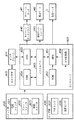
<インクジェット記録装置の制御構成(図3)>
図3は図1に示した記録装置の制御構成を示すブロック図である。
<Control Configuration of Inkjet Recording Apparatus (FIG. 3)>
FIG. 3 is a block diagram showing a control configuration of the recording apparatus shown in FIG.
図3に示すように、コントローラ600は、MPU601、後述する制御シーケンスに対応したプログラム、所要のテーブル、その他の固定データを格納したROM602、キャリッジモータM1の制御、搬送モータM2の制御、及び、記録ヘッド3の制御のための制御信号を生成する特殊用途集積回路(ASIC)603、画像データの展開領域やプログラム実行のための作業用領域等を設けたRAM604、MPU601、ASIC603、RAM604を相互に接続してデータの授受を行うシステムバス605、以下に説明するセンサ群からのアナログ信号を入力してA/D変換し、デジタル信号をMPU601に供給するA/D変換器606などで構成される。
As shown in FIG. 3, the
また、図2において、610は画像データの供給源となるコンピュータ(或いは、画像読取り用のリーダやデジタルカメラなど)でありホスト装置と総称される。ホスト装置610と記録装置1との間ではインタフェース(I/F)611を介して画像データ、コマンド、ステータス信号等を送受信する。
In FIG. 2,
さらに、620はスイッチ群であり、電源スイッチ621、プリント開始を指令するためのプリントスイッチ622、及び記録ヘッド3のインク吐出性能を良好な状態に維持するための処理(回復処理)の起動を指示するための回復スイッチ623など、操作者による指令入力を受けるためのスイッチから構成される。630はホームポジションhを検出するためのフォトカプラなどの位置センサ631、環境温度を検出するために記録装置の適宜の箇所に設けられた温度センサ632等から構成される装置状態を検出するためのセンサ群である。
Further,
さらに、640はキャリッジ2を矢印A方向に往復走査させるためのキャリッジモータM1を駆動させるキャリッジモータドライバ、642は記録媒体Pを搬送するための搬送モータM2を駆動させる搬送モータドライバである。
Further, 640 is a carriage motor driver that drives a carriage motor M1 for reciprocating scanning of the
ASIC603は、記録ヘッド3による記録走査の際に、RAM602の記憶領域に直接アクセスしながら記録ヘッドに対して記録素子(ヒータ)の駆動データ(DATA)を転送する。
The
次に、上記構成の記録装置の記録ヘッドに用いられるヘッド基板についてのいくつかの実施例について説明する。特に、ヘッド基板上(ヒータボード上)に作りこまれる駆動回路の構成を中心に説明する。 Next, some examples of the head substrate used in the recording head of the recording apparatus having the above configuration will be described. In particular, the configuration of the drive circuit built on the head substrate (on the heater board) will be mainly described.
なお、基板の上には各記録素子に対応してインク吐出口やこのインク吐出口に連通した流路を形成する部材(不図示)が設けられており、これにより記録ヘッドを構成する。 On the substrate, an ink discharge port and a member (not shown) that forms a flow path communicating with the ink discharge port are provided corresponding to each recording element, thereby constituting a recording head.
そして、この記録素子上に供給されるインクを記録素子の駆動によって加熱することで膜沸騰による気泡を発生させインクを吐出口から吐出する構成となっている。 The ink supplied onto the recording element is heated by driving the recording element to generate bubbles due to film boiling, and the ink is ejected from the ejection port.
図4は本発明の実施例1に従うヒータ周辺回路の1ビット分の回路120の構成を示す図である。なお、図4において、既に従来例において言及したのと同じ構成要素には同じ参照番号を付し、その説明は省略する。
FIG. 4 is a diagram showing a configuration of the
図4に示されているように、ヒータ101の両端のノードはMOSトランジスタからなるビットセレクトスイッチ110及び111、MOSトランジスタからなるテストセレクトスイッチ112及び113を介し、モニタ出力端子115及び116へと接続されている。
As shown in FIG. 4, the nodes at both ends of the
なお、この実施例では、ビットセレクトスイッチ110が(+)側でビットセレクトスイッチ111が(−)側になり、テストセレクトスイッチ112が(+)側でテストセレクトスイッチ113が(−)側になっている。また、モニタ出力端子115が(+)側でモニタ出力端子116が(−)側になっている。
In this embodiment, the bit
また、図4から分かるように、ビットセレクトスイッチ110と111のゲート端子107は内部回路からの素子選択出力が接続されており、テストセレクトスイッチ112と113のゲートは外部から印加されるテストセレクト端子114を介して論理信号(TEST)が入力される。なお、テストセレクトスイッチ112、113のゲートに印加される信号は、テストセレクト端子114からの信号が直接印加されてもよいし、何らかの論理演算を行った信号が入力されるものでもよい。
As can be seen from FIG. 4, the element selection output from the internal circuit is connected to the
図5は図4に示した1ビット分の回路120が複数並んだヒータ周辺回路の構成を示す図である。なお、図5においても、既に従来例において言及したのと同じ構成要素には同じ参照番号を付し、その説明は省略する。
FIG. 5 is a diagram showing a configuration of a heater peripheral circuit in which a plurality of 1-
図5では、図4で説明した1ビット分の回路120を破線内に示しており、この1ビット回路が複数配置されていることが示されている。
In FIG. 5, the
図5から分かるように、複数の1ビット回路120各々に含まれるヒータの両端ノードは、図4を参照してビットセレクトスイッチ110〜111、テストセレクトスイッチ112〜113を介し、モニタ出力端子115および116へと接続されている。
As can be seen from FIG. 5, both end nodes of the heaters included in each of the plurality of 1-
ビットセレクトスイッチ110〜111のゲートは、各1ビット回路の内部回路からの素子選択出力が接続されている。
The gates of the bit
また、テストセレクト端子114は各1ビット回路120のテストセレクトスイッチ112〜113のゲートへと共通に入力されている。
The test
次に、以上のような構成の回路の動作についてフローチャートを参照して説明する。 Next, the operation of the circuit having the above configuration will be described with reference to a flowchart.
図6は実施例1に従う抵抗測定手順を示すフローチャートである。 FIG. 6 is a flowchart showing a resistance measurement procedure according to the first embodiment.
まず、ステップS10ではヒータにて発生するパワーを測定しようとする任意の1つの1ビット回路120を内部回路からのゲート端子107を介した素子選択出力により選択する。
First, in step S10, any one 1-
さらに、ステップS20では、テストセレクト端子114にテストセレクトスイッチ112〜113についてもオンとなる論理信号(TEST)を印加する。
Further, in step S20, a logic signal (TEST) that turns on the test
ここで、テストセレクトスイッチは全てのビットでオン状態となっているが、選択した任意の1つのビットセレクトスイッチのみがオン状態となっているため、モニタ出力端子115と116には選択したビットのヒータの両端の電位(V1,V2)が出力されることとなる。
Here, the test select switch is turned on in all bits, but since only one selected bit select switch is turned on, the
ステップS30ではヒータに電流を導通し、その電流値(I)とヒータ両端の差電圧値(V1−V2)を測定する。 In step S30, a current is conducted to the heater, and the current value (I) and the difference voltage value (V1-V2) across the heater are measured.
そして、ステップS40では、ステップS30で得られた値からヒータで発生するパワーを求める。 In step S40, the power generated by the heater is obtained from the value obtained in step S30.
ステップS50では、全ての記録素子(ヒータ)についての測定が終了したかどうかを調べ、測定未終了であれば、処理はステップS10に戻り、素子選択出力を次の1ビット回路120のゲート端子107に入力して測定対象を選択し、前述の処理を繰り返す。これに対し、測定終了と判断されれば処理を終了する。
In step S50, it is checked whether or not the measurement for all the printing elements (heaters) has been completed. If the measurement has not been completed, the process returns to step S10, and the element selection output is sent to the
このように測定を、順次各ビットに対して行うことで、従来の配線抵抗やトランジスタのオン抵抗を含めた抵抗ばらつきのみではなく、ヒータで発生するパワーのばらつきを求めることができる。その結果、そのばらつき許容範囲を従来よりも大きくすることにより歩留まり向上を達成できる。 Thus, by sequentially performing the measurement on each bit, not only the resistance variation including the conventional wiring resistance and the on-resistance of the transistor but also the power variation generated by the heater can be obtained. As a result, a yield improvement can be achieved by making the variation allowable range larger than before.
図7は本発明の実施例2に従うヒータ周辺回路の1ビット分の回路120の構成を示す図である。なお、図7において、既に従来例や実施例1において言及したのと同じ構成要素には同じ参照番号を付し、その説明は省略する。
FIG. 7 is a diagram showing a configuration of a
この実施例の特徴は、実施例1の構成がヒータの両端の電位がモニタ端子へ引き出し可能となっていたのに対し、一方の端子のみを引き出す構成とし簡略化を図った点である。 The feature of this embodiment is that the potential of both ends of the heater can be pulled out to the monitor terminal in the configuration of the first embodiment, but only one terminal is pulled out for simplification.
即ち、図7に示す構成によれば、ヒータ101のドライバトランスタ102側のノードはビットセレクトスイッチ111、テストセレクトスイッチ113を介し、モニタ出力端子116へと接続されている。ここで、ビットセレクトスイッチ111のゲートはゲート端子107を介して内部回路からの素子選択出力が接続されており、テストセレクトスイッチ113のゲートは外部から印加されるテストセレクト端子114からの論理信号(TEST)が接続されている。なお、テストセレクトスイッチ113のゲートに印加される信号は、テストセレクト端子114からの信号が直接印加されてもよいし、何らかの論理演算を行った信号が入力されるものでもよい。この点は実施例1と同様である。
That is, according to the configuration shown in FIG. 7, the node on the
図8は図7に示した1ビット分の回路120が複数並んだヒータ周辺回路の構成を示す図である。なお、図8においても、既に従来例や実施例1において言及したのと同じ構成要素には同じ参照番号を付し、その説明は省略する。
FIG. 8 is a diagram showing a configuration of a heater peripheral circuit in which a plurality of 1-
図8では、図7で説明した1ビット分の回路120を破線内に示しており、この1ビット回路が複数配置されていることが示されている。
In FIG. 8, the
図8に示す構成によれば、複数の1ビット回路120各々に含まれるヒータ101のドライバトランジスタ102側のノードはビットセレクトスイッチ111、テストセレクトスイッチ113を介し、モニタ出力端子116へと接続されている。ビットセレクトスイッチ111のゲートにはゲート端子107を介して、実施例1と同様に素子選択出力が入力されている。テストセレクト端子114は各1ビット回路120のテストセレクトスイッチ113のゲートへと共通に入力されている。
According to the configuration shown in FIG. 8, the node on the
次に、以上のような構成の回路の動作について説明する。 Next, the operation of the circuit configured as described above will be described.
実施例2でも実施例1と同様にテストセレクトスイッチをオンとし、任意の1つのビットセレクトスイッチをオンすることで、ヒータのドライバトランジスタ側のノード電位がモニタ出力端子116へと出力される。後の手順は実施例1と同様である。
In the second embodiment, the node potential on the driver transistor side of the heater is output to the
この実施例は、電源端子(VH)105側に存在する寄生抵抗103が、ドライバトランジスタのオン抵抗および電源端子(GNDH)106側に存在する寄生抵抗104の合計抵抗及びヒータ101の抵抗値に対して十分小さいもので、ヒータ101で発生するパワーを測定する上で問題ない場合に適用できる。その場合、ヒータボードのレイアウト面積を抑制することが可能となるという利点がある。
In this embodiment, the
ここで、ドライバトランジスタ側の電位を引き出す構成としている理由としては次のようなことがある。即ち、ドライバトランジスタ102のオン抵抗を十分小さくするためにはそのサイズを大きくする必要があり、これにはヒータボード設計上限界があるため、ドライバトランジスタ102のオン抵抗は一定の値を有するものとなり、その抵抗値のばらつきがヒータで発生するパワーのばらつき測定に対する影響を無視することは困難な場合が多い。一方、電源端子(VH)側の配線抵抗に寄生する抵抗は、その配線の膜厚を増加するなどの手段により抑制することが可能である。
Here, the reason why the configuration is such that the potential on the driver transistor side is extracted is as follows. In other words, in order to sufficiently reduce the on-resistance of the
その場合、この実施例のようにヒータ101とドライバトランジスタ102の間のノードの電位が測定できる構成であれば、トランジスタのオン抵抗成分および電源端子(GNDH)側の配線抵抗成分を除去した抵抗成分を測定可能となるため、そのばらつき許容範囲は従来に比較して大きくすることが可能となり、歩留まりの向上が図られる。
In this case, if the configuration is such that the potential of the node between the
また、電源端子(VH)配線側の寄生抵抗603がヒータ101の抵抗およびトランジスタ102のオン抵抗などに対して十分小さいものであれば、電源端子(VH)105とモニタ端子116の差電圧(VH−V2)、及びヒータ101に流れる電流(I)から測定されるパワーをほぼヒータで発生するパワーと見なすことが可能となる。このような場合、実施例2の構成は、実施例1のそれに比べ素子数を減らすことが可能になるので、ヒータボードのレイアウト面積を抑制しつつ、歩留まりの向上が達成できる。
If the
なお、実施例1〜2では、図示した全てのビットのヒータ両端の電位が引き出し可能とした構成を示しているが、本発明はこの引き出しを全てのビットに対して行わなければならないものではなく、例えば、複数ビット間隔で間歇的に引き出しを行ってたとしても、その測定から得られるヒータで発生するパワーのばらつきから許容範囲を評価することができるので、その効果は依然として有効である。 In the first and second embodiments, a configuration is shown in which the potentials across the heaters of all the illustrated bits can be extracted. However, the present invention does not require this extraction to be performed for all the bits. For example, even if the extraction is intermittently performed at intervals of a plurality of bits, the allowable range can be evaluated from the variation in power generated by the heater obtained from the measurement, and the effect is still effective.
なぜなら、通常、半導体集積回路技術により高密度に配置されたヒータやドライバトランジスタでは隣接した素子間でその特性に急峻な変化があるものではない場合が多く、たとえ、数ビット毎の特性を抜取って測定としたとしても、ヒータボード内でのヒータで発生するパワーのばらつきを一定の確度を持ちつつ把握することが可能であるであるからである。また、測定のためのスイッチ素子を各ヒータに配置するには、一定のレイアウト面積が必要となるため、この面積を抑制する目的で複数ビット間隔にスイッチ素子を配置し、必要とされる測定確度を維持しつつ、レイアウト面積の増加を抑制することができるという利点もあるからである。 This is because, in general, heaters and driver transistors arranged at a high density by semiconductor integrated circuit technology often do not have a sharp change in characteristics between adjacent elements. This is because it is possible to grasp the variation in power generated by the heater in the heater board with a certain degree of accuracy. In addition, since a certain layout area is required to arrange the switch elements for measurement in each heater, the switch elements are arranged at intervals of multiple bits in order to suppress this area, and the required measurement accuracy This is because there is an advantage that an increase in layout area can be suppressed while maintaining the above.
さらに、以上の実施例において、記録ヘッドから吐出される液滴はインクであるとして説明し、さらにインクタンクに収容される液体はインクであるとして説明したが、その収容物はインクに限定されるものではない。例えば、記録画像の定着性や耐水性を高めたり、その画像品質を高めたりするために記録媒体に対して吐出される処理液のようなものがインクタンクに収容されていても良い。 Furthermore, in the above embodiments, the liquid droplets ejected from the recording head have been described as ink, and the liquid stored in the ink tank has been described as ink. However, the storage is limited to ink. It is not a thing. For example, a treatment liquid discharged to the recording medium may be accommodated in the ink tank in order to improve the fixability and water resistance of the recorded image or to improve the image quality.
以上の実施例は、特にインクジェット記録方式の中でも、インク吐出を行わせるために利用されるエネルギーとして熱エネルギーを発生する手段(例えば電気熱変換体やレーザ光等)を備え、前記熱エネルギーによりインクの状態変化を生起させる方式を用いることにより記録の高密度化、高精細化が達成できる。 The above embodiment includes means (for example, an electrothermal converter or a laser beam) that generates thermal energy as energy used to perform ink ejection, particularly in the ink jet recording system, and the ink is generated by the thermal energy. By using a system that causes a change in the state of recording, it is possible to achieve higher recording density and higher definition.
また以上の実施例はシリアルスキャンタイプのインクジェット記録装置を例として説明したが、本発明はこれに限らず、記録可能な記録媒体の最大幅の長さを持つフルライン記録ヘッドを用いたインクジェット記録装置にも、本発明は有効に適用できる。そのような記録ヘッドとしては、複数の記録ヘッドの組合せによってその長さを満たす構成や、一体的に形成された1個の記録ヘッドとしての構成のいずれでもよい。 In the above embodiment, the serial scan type inkjet recording apparatus has been described as an example. However, the present invention is not limited to this, and inkjet recording using a full line recording head having the maximum width of a recordable recording medium. The present invention can be effectively applied to an apparatus. As such a recording head, either a configuration satisfying the length by a combination of a plurality of recording heads or a configuration as a single recording head formed integrally may be used.
加えて、以上の実施例のようなシリアルスキャンタイプのものでも、装置本体に固定された記録ヘッド、あるいは装置本体に装着されることで装置本体との電気的な接続や装置本体からのインクの供給が可能になる交換自在のカートリッジタイプの記録ヘッドを用いた場合にも本発明は有効である。 In addition, even the serial scan type as in the above-described embodiments is mounted on the recording head fixed to the apparatus main body or the apparatus main body so that the electrical connection with the apparatus main body and the ink from the apparatus main body The present invention is also effective when an exchangeable cartridge type recording head that can be supplied is used.
さらに加えて、本発明のインクジェット記録装置の形態としては、コンピュータ等の情報処理機器の画像出力装置として用いられるものの他、リーダ等と組合せた複写装置、さらには送受信機能を有するファクシミリ装置の形態を採るもの等であってもよい。 In addition, the ink jet recording apparatus according to the present invention may be used as an image output apparatus for information processing equipment such as a computer, a copying apparatus combined with a reader, or a facsimile apparatus having a transmission / reception function. It may be one taken.
101 ヒータ
102 ドライバトランジスタ
103、104 配線抵抗
105、106 電源端子
107 内部回路からの素子選択出力
108 寄生抵抗
110、111 ビットセレクトスイッチ
112、113 テストセレクトスイッチ
114 テストセレクト端子
115、116 モニタ出力端子
120 1ビットヒータ周辺回路
101
Claims (13)
前記複数の記録素子にテスト信号を入力する第1の端子と、
前記複数の記録素子の少なくとも一部の記録素子に関し、該記録素子を選択駆動する選択信号を入力する第2の端子と、
前記選択信号により選択された記録素子の少なくとも一端の電位を出力する第3の端子とを有することを特徴とするヘッド基板。 A head substrate comprising a plurality of recording elements and a plurality of driving elements for driving the plurality of recording elements,
A first terminal for inputting a test signal to the plurality of recording elements;
A second terminal for inputting a selection signal for selectively driving the recording elements with respect to at least some of the plurality of recording elements;
And a third terminal for outputting a potential of at least one end of the recording element selected by the selection signal.
前記テスト信号により記録素子に通電するための第3のMOSトランジスタとをさらに有することを特徴とする請求項3に記載のヘッド基板。 A second MOS transistor for selecting a recording element according to the selection signal;
The head substrate according to claim 3, further comprising a third MOS transistor for energizing the recording element by the test signal.
前記テスト信号は前記第3のMOSトランジスタのゲートに入力されることを特徴とする請求項4に記載のヘッド基板。 The selection signal is commonly input to the gates of the first and second MOS transistors,
The head substrate according to claim 4, wherein the test signal is input to a gate of the third MOS transistor.
前記第4のMOSトランジスタのゲートには前記選択信号が、前記第5のMOSトランジスタには前記テスト信号が入力されることを特徴とする請求項7に記載のヘッド基板。 A fourth and a fifth MOS transistor connected in series between a side connecting a common power source to the plurality of recording elements and the fourth terminal;
The head substrate according to claim 7, wherein the selection signal is input to a gate of the fourth MOS transistor and the test signal is input to the fifth MOS transistor.
A recording apparatus that performs recording using the recording head according to claim 9 or the head cartridge according to claim 12.
Priority Applications (3)
| Application Number | Priority Date | Filing Date | Title |
|---|---|---|---|
| JP2004339443A JP2006142780A (en) | 2004-11-24 | 2004-11-24 | Head substrate, recording head, head cartridge, and recorder using recording head or head cartridge |
| US11/274,142 US7452050B2 (en) | 2004-11-24 | 2005-11-16 | Head substrate, printhead, head cartridge, and printing apparatus using the printhead or head cartridge |
| US12/127,267 US7762646B2 (en) | 2004-11-24 | 2008-05-27 | Head substrate, printhead, head cartridge, and printing apparatus using the printhead or head cartridge |
Applications Claiming Priority (1)
| Application Number | Priority Date | Filing Date | Title |
|---|---|---|---|
| JP2004339443A JP2006142780A (en) | 2004-11-24 | 2004-11-24 | Head substrate, recording head, head cartridge, and recorder using recording head or head cartridge |
Publications (2)
| Publication Number | Publication Date |
|---|---|
| JP2006142780A true JP2006142780A (en) | 2006-06-08 |
| JP2006142780A5 JP2006142780A5 (en) | 2008-01-17 |
Family
ID=36460536
Family Applications (1)
| Application Number | Title | Priority Date | Filing Date |
|---|---|---|---|
| JP2004339443A Abandoned JP2006142780A (en) | 2004-11-24 | 2004-11-24 | Head substrate, recording head, head cartridge, and recorder using recording head or head cartridge |
Country Status (2)
| Country | Link |
|---|---|
| US (2) | US7452050B2 (en) |
| JP (1) | JP2006142780A (en) |
Families Citing this family (1)
| Publication number | Priority date | Publication date | Assignee | Title |
|---|---|---|---|---|
| JP4933057B2 (en) * | 2005-05-13 | 2012-05-16 | キヤノン株式会社 | Head substrate, recording head, and recording apparatus |
Family Cites Families (4)
| Publication number | Priority date | Publication date | Assignee | Title |
|---|---|---|---|---|
| JPH05238038A (en) | 1992-02-28 | 1993-09-17 | Nec Corp | Control system of resistance measurement of thermal head |
| US6116717A (en) * | 1998-09-15 | 2000-09-12 | Lexmark International, Inc. | Method and apparatus for customized control of a print cartridge |
| ATE301545T1 (en) | 2001-04-27 | 2005-08-15 | Canon Kk | PRINTING APPARATUS AND PRESSURE CONTROL METHOD |
| JP4266569B2 (en) | 2001-04-27 | 2009-05-20 | キヤノン株式会社 | Recording apparatus and recording control method for recording apparatus |
-
2004
- 2004-11-24 JP JP2004339443A patent/JP2006142780A/en not_active Abandoned
-
2005
- 2005-11-16 US US11/274,142 patent/US7452050B2/en not_active Expired - Fee Related
-
2008
- 2008-05-27 US US12/127,267 patent/US7762646B2/en not_active Expired - Fee Related
Also Published As
| Publication number | Publication date |
|---|---|
| US7452050B2 (en) | 2008-11-18 |
| US20080231663A1 (en) | 2008-09-25 |
| US7762646B2 (en) | 2010-07-27 |
| US20060109292A1 (en) | 2006-05-25 |
Similar Documents
| Publication | Publication Date | Title |
|---|---|---|
| JP4989433B2 (en) | Head substrate, recording head, head cartridge, and recording apparatus | |
| JP4933057B2 (en) | Head substrate, recording head, and recording apparatus | |
| JP5184869B2 (en) | Head substrate, recording head, head cartridge, and recording apparatus | |
| JP5032964B2 (en) | Head substrate, recording head, head cartridge, and recording apparatus | |
| JP5064990B2 (en) | Recording head, head cartridge, recording apparatus | |
| JP4596757B2 (en) | Recording head test equipment | |
| JP4785375B2 (en) | Inkjet recording head substrate, recording head, head cartridge, and recording apparatus | |
| JP4502358B2 (en) | RECORDING HEAD SUBSTRATE, RECORDING HEAD, AND RECORDING DEVICE | |
| JP4546102B2 (en) | Recording head substrate, recording head using the recording head substrate, recording apparatus including the recording head, and head cartridge including the recording head | |
| JP4678825B2 (en) | Head substrate, recording head, head cartridge, and recording apparatus using the recording head or head cartridge | |
| JP4799389B2 (en) | Head substrate, recording head, head cartridge, and recording apparatus | |
| JP2006159780A (en) | Substrate for ink jet recording head and drive control method, ink jet recording head, ink jet recording head cartridge and ink jet recorder | |
| JP6397258B2 (en) | Element substrate, liquid discharge head, and recording apparatus | |
| JP2006142780A (en) | Head substrate, recording head, head cartridge, and recorder using recording head or head cartridge | |
| JP4532890B2 (en) | Recording head and recording apparatus provided with the recording head | |
| JP5571888B2 (en) | Head substrate, recording head, head cartridge | |
| JP2010131862A (en) | Head substrate and inkjet recording head | |
| JP2005169867A (en) | Recording head element substrate, recording head and recording device | |
| JP4455013B2 (en) | Recording head driving method, recording head, and recording apparatus | |
| JP4289976B2 (en) | Recording head driving method, recording head element substrate, recording head, head cartridge, and recording apparatus | |
| JP5230093B2 (en) | Element substrate, recording head, recording apparatus | |
| JP2020023077A (en) | Element substrate, recording head, and recording device | |
| JP2006096007A (en) | Head substrate, recording head, head cartridge, and recorder | |
| JP2019171625A (en) | Recording element substrate, recording device, and method for inspection of recording element substrate | |
| JP2005169866A (en) | Recording head and recording apparatus using it |
Legal Events
| Date | Code | Title | Description |
|---|---|---|---|
| A521 | Request for written amendment filed |
Free format text: JAPANESE INTERMEDIATE CODE: A523 Effective date: 20071122 |
|
| A621 | Written request for application examination |
Free format text: JAPANESE INTERMEDIATE CODE: A621 Effective date: 20071122 |
|
| RD03 | Notification of appointment of power of attorney |
Free format text: JAPANESE INTERMEDIATE CODE: A7423 Effective date: 20071122 |
|
| A762 | Written abandonment of application |
Free format text: JAPANESE INTERMEDIATE CODE: A762 Effective date: 20100617 |
|
| A977 | Report on retrieval |
Free format text: JAPANESE INTERMEDIATE CODE: A971007 Effective date: 20100625 |