JP5230093B2 - Element substrate, recording head, recording apparatus - Google Patents
Element substrate, recording head, recording apparatus Download PDFInfo
- Publication number
- JP5230093B2 JP5230093B2 JP2006333861A JP2006333861A JP5230093B2 JP 5230093 B2 JP5230093 B2 JP 5230093B2 JP 2006333861 A JP2006333861 A JP 2006333861A JP 2006333861 A JP2006333861 A JP 2006333861A JP 5230093 B2 JP5230093 B2 JP 5230093B2
- Authority
- JP
- Japan
- Prior art keywords
- voltage
- heater
- recording
- element substrate
- recording head
- Prior art date
- Legal status (The legal status is an assumption and is not a legal conclusion. Google has not performed a legal analysis and makes no representation as to the accuracy of the status listed.)
- Active
Links
Images


Description
本発明は、インクを吐出する記録素子とこれを駆動するための駆動回路等を有する素子基板及びこれを用いた記録ヘッド、記録装置に関する。 The present invention relates to a recording element and the element substrate and the recording head using the same having a driving circuit for driving the for ejecting ink to a record apparatus.
従来から、インクジェット方式に従う記録ヘッドの電気熱変換素子(ヒータ)とその駆動回路は、半導体プロセス技術を用いて同一基板上に形成されている(特許文献1参照)。ヒータと駆動回路とが一体形成された素子基板は、様々な配置されたものが開示されている。図3は、その一例であり、電源端子や信号端子のパッド110は、素子基板の短辺側に配置されていて、そこから素子基板内部の各回路へアルミニウム(Al)配線(不図示)で接続されている。
2. Description of the Related Art Conventionally, an electrothermal conversion element (heater) of a recording head according to an ink jet system and a drive circuit thereof are formed on the same substrate using a semiconductor process technology (see Patent Document 1). Various element substrates in which a heater and a drive circuit are integrally formed are disclosed. FIG. 3 shows an example of this. The
また、ヒータ電流の駆動回路としてNMOSトランジスタによるパワートランジスタを採用した記録ヘッドがある。この記録ヘッドにおいて、NMOSトランジスタのドライバビリティを向上させるために、論理回路の電源電圧(例えば3.3Vや5Vなど)を昇圧してNMOSトランジスタのゲートに印加する構成が開示されている(特許文献2参照)。 In addition, there is a recording head that employs a power transistor using an NMOS transistor as a heater current driving circuit. In this recording head, in order to improve the drivability of the NMOS transistor, a configuration is disclosed in which the power supply voltage (eg, 3.3 V or 5 V) of the logic circuit is boosted and applied to the gate of the NMOS transistor (Patent Document). 2).
図6は、従来の、記録素子としてのヒータ、ドライバトランジスタ等を含む1セグメントの等価回路の一例を示す図である。 FIG. 6 is a diagram illustrating an example of a conventional one-segment equivalent circuit including a heater, a driver transistor, and the like as a recording element.
ヒータ駆動信号は、不図示のシフトレジスタ(S/R)やデコーダ等を経て、論理回路の電源電圧VDDの振幅をもってヒータ選択回路120から出力される。このヒータ駆動信号は、レベル変換部121において論理回路電源電圧VDDよりも高い、ドライバ駆動電圧VHTMの振幅に昇圧され、ドライバ駆動バッファ122を経て、ドライバトランジスタ123のゲートに入力する。これは、ドライバトランジスタ123のゲートを論理回路の電源電圧よりも高い電圧で駆動することで、ヒータ124駆動時のドライバトランジスタ123での実効的な抵抗を小さくするためである。なお、ドライバ駆動電圧VHTMはプリンタ本体から入力されるヒータ電源電圧VHと同電位の電圧VHTから、素子基板内部に配置した変換電圧発生部125により生成される。
The heater drive signal is output from the
図7は、変換電圧発生部と記録ヘッドの素子基板に設けられた複数セグメントの駆動回路との関係を示す図である。 FIG. 7 is a diagram illustrating a relationship between the conversion voltage generation unit and a multi-segment drive circuit provided on the element substrate of the recording head.
図7に示すように、M個のセグメント毎に、レベル変換部、ドライバ駆動バッファ及びドライバトランジスタ123とが備えられ、各セグメントは、不図示のヒータ選択回路からの信号を入力する。また、変換電圧発生部125は、素子基板内に少なくとも1つ設けられ、駆動回路に、ヒータ電源電圧VHと同電位の電圧VHTから生成したドライバ駆動電圧VHTMを入力する。
As shown in FIG. 7, a level conversion unit, a driver drive buffer, and a
図8に、従来から用いられている変換電圧発生部の回路図を示す。 FIG. 8 shows a circuit diagram of a conversion voltage generator conventionally used.
図8の変換電圧発生部125は、抵抗130および131の抵抗比によって設定された所望の電圧を電源供給用のMOSトランジスタ132のゲートへ印加するソースフォロア回路によってドライバ駆動電圧VHTMを出力する構成である。抵抗130、131の抵抗値の比と、ヒータ電源電圧VHと同電位の電圧VHTとにより、ドライバ駆動電圧VHTMの電圧値が固定的に決定される。
8 has a configuration in which a driver drive voltage VHTM is output by a source follower circuit that applies a desired voltage set by the resistance ratio of the
以上のように、インクジェット記録ヘッド用素子基板の回路は、入力信号の振幅である論理回路の電源電圧VDDと、MOSトランジスタのゲートに印加するためのより高い電圧であるドライバ駆動電圧VHTMとの、2種類の電圧により制御及び駆動される。そして、論理回路の電源電圧VDDに相当する入力信号の振幅を、レベル変換部でドライバ駆動電圧VHTMに相当する振幅に変換している。 As described above, the circuit of the element substrate for the inkjet recording head includes the power supply voltage VDD of the logic circuit that is the amplitude of the input signal and the driver drive voltage VHTM that is a higher voltage to be applied to the gate of the MOS transistor. Controlled and driven by two types of voltages. The amplitude of the input signal corresponding to the power supply voltage VDD of the logic circuit is converted into an amplitude corresponding to the driver drive voltage VHTM by the level conversion unit.
ここで、論理回路の電源電圧VDDは、記録ヘッド用素子基板へ、記録装置本体から入力される。一方、ドライバ駆動電圧VHTMは、記録装置本体から入力されるヒータを駆動するためのヒータ電源電圧VHと同電位の電圧VHTから、素子基板内の変換電圧発生部において生成している。なお、ドライバ駆動電圧VHTMは、素子基板内のトランジスタ等の素子の耐圧を考慮した上で、所望の条件でヒータ駆動用のMOSトランジスタをオンさせることができる電圧に設定している。
ところで、以上述べてきたようなインクジェット記録装置には、同一のヘッドから異なる液滴サイズのインクを吐出する構成をとるものがある。 Incidentally, some of the ink jet recording apparatuses as described above are configured to eject inks having different droplet sizes from the same head.
このような記録装置では、所望の液滴サイズのインクを吐出するために、ヒータの抵抗値やヒータサイズなどが設計される。そして、理想的な吐出条件を実現するためには、ヒータの抵抗値やサイズに合わせて、ヒータに入力する電流の通電時間やヒータに印加する電圧などを変化させ、ヒータで発生する熱量を調整することが望まれる。しかしながら、ヒータの電源電圧は記録装置本体から記録ヘッドの素子基板へ入力されるものであるため、この電源電圧などを調整する手段を設けることはコストの上昇を招く場合がある。このため、従来は、主にヒータに入力する電流の通電時間を変化させることで発生する熱量の調整を行ってきた。 In such a recording apparatus, a heater resistance value, a heater size, and the like are designed in order to eject ink having a desired droplet size. In order to realize ideal discharge conditions, the amount of heat generated by the heater is adjusted by changing the energizing time of the current input to the heater and the voltage applied to the heater according to the resistance value and size of the heater. It is desirable to do. However, since the power supply voltage of the heater is input from the printing apparatus main body to the element substrate of the printhead, providing a means for adjusting the power supply voltage or the like may increase the cost. For this reason, conventionally, the amount of heat generated has been adjusted mainly by changing the energization time of the current input to the heater.
しかしながら、ヒータに入力する電流の通電時間を長く設定すると、吐出間隔が長くなるため、高速で記録を行うことが困難となる場合がある。また、ヒータに入力する電流の通電時間の変化が、ヒータからインクへの熱伝達特性を変化させ、高画質な記録を妨げる場合があった。このため、ヒータに入力する電流の通電時間の制御は限られてしまう。 However, if the energization time of the current input to the heater is set to be long, the discharge interval becomes long, and it may be difficult to perform recording at high speed. In addition, a change in the energization time of the current input to the heater may change the heat transfer characteristics from the heater to the ink, thereby preventing high-quality recording. For this reason, control of the energization time of the current input to the heater is limited.
また、異なる液滴サイズのインクを吐出する構成をとる記録装置でなくても、記録ヘッドやインクの温度及び同時に吐出するノズル数等が変化する場合、ヒータで発生する熱量を調整することが必要となる場合がある。 Even if the recording device is not configured to eject ink of different droplet sizes, it is necessary to adjust the amount of heat generated by the heater when the temperature of the recording head or ink, the number of nozzles ejected simultaneously, and the like change. It may become.
さらに、製造時のヒータ抵抗のバラツキや駆動回路の抵抗バラツキによる、吐出不良を回避するためにも、ヒータで発生する熱量を調整することが必要となる場合がある。 Furthermore, it may be necessary to adjust the amount of heat generated in the heater in order to avoid ejection defects due to variations in heater resistance during manufacturing and resistance variations in the drive circuit.
これらヒータで発生する熱量を調整する場合も、ヒータに入力する電流の通電時間の制御は限られてしまい、この制御で調整できない素子基板は不良品となることから、製造歩留まりを低下させる要因ともなる。 Even when adjusting the amount of heat generated by these heaters, the control of the energization time of the current input to the heater is limited, and the element substrate that cannot be adjusted by this control becomes a defective product, which may cause a reduction in manufacturing yield. Become.
本発明は以上の点に鑑み、記録素子に入力する電流の通電時間を制御すること以外に、記録素子で発生するインクを吐出させるためのエネルギーを調整する手段を有する素子基板を提供することを目的としている。 In view of the above, the present invention provides an element substrate having means for adjusting energy for discharging ink generated in a recording element, in addition to controlling the energization time of a current input to the recording element. It is aimed.
上記の目的を達成するための本発明は、複数のヒータと、前記複数のヒータのそれぞれに対応して設けられるとともに、ゲートに入力された電圧に従って前記ヒータの駆動のスイッチングを行う複数のMOSトランジスタとを備えた記録ヘッド用の素子基板であって、外部からシリアルに入力され、各ビットが前記複数のヒータの1つに対応したデジタル画像データを格納するシフトレジスタと、ヒータ駆動信号を生成するヒータ選択回路と、前記ヒータ駆動信号を昇圧して前記MOSトランジスタのゲートへ印加するレベル変換回路と、前記シフトレジスタに格納されたデジタル画像データの各ビットがオンとなるビット数に応じた電圧を発生する電圧発生回路とを備え、前記電圧発生回路は、前記発生した電圧をゲートに入力し、前記複数のヒータに印加される電圧と同電位の電圧をドレインに入力し、該ゲートに入力された電圧に従って、ソースからの出力電圧を変化させるNMOSトランジスタを含み、前記レベル変換回路は、前記ソースからの出力電圧に従って、前記ヒータ駆動信号の昇圧を行うことを特徴とする。 To achieve the above object, the present invention provides a plurality of heaters and a plurality of MOS transistors provided corresponding to each of the plurality of heaters and switching the driving of the heaters according to a voltage input to a gate. And a shift register for storing digital image data corresponding to one of the plurality of heaters, and a heater driving signal. A heater selection circuit, a level conversion circuit that boosts the heater drive signal and applies it to the gate of the MOS transistor, and a voltage corresponding to the number of bits in which each bit of the digital image data stored in the shift register is turned on and a voltage generating circuit that occurs, the voltage generating circuit receives the generated voltage to the gate, the double A voltage having the same potential as the voltage applied to the heater is input to the drain, and an NMOS transistor that changes an output voltage from the source according to the voltage input to the gate is included. The heater drive signal is boosted according to the output voltage .
また、上記の目的を達成するための別の本発明は、上記素子基板を有する記録ヘッド、記録装置である。 Further, another aspect of the present invention for achieving the above object, a recording head having the element substrate, a record apparatus.
本発明によれば、記録素子に入力する電流の通電時間を制御すること以外に、記録素子で発生するインクを吐出させるためのエネルギーを調整する手段を有する記録素子を提供することができるという効果がある。 According to the present invention, in addition to controlling the energization time of the current input to the recording element, it is possible to provide a recording element having means for adjusting energy for discharging ink generated in the recording element. There is.
以下添付図面を参照して本発明の好適な実施形態について詳細に説明する。 Preferred embodiments of the present invention will be described below in detail with reference to the accompanying drawings.
なお、この明細書において、「記録」とは、文字、図形等有意の情報を形成する場合のみならず、有意無意を問わず、広く記録媒体上に画像、模様、パターン等を形成する、または媒体の加工を行う場合も表すものとする。また、人間が視覚で知覚し得るように顕在化したものであるか否かを問わない。 In this specification, “recording” not only forms significant information such as characters and graphics, but also forms images, patterns, patterns, etc. on a wide variety of recording media, regardless of significance, or It also represents the case where the medium is processed. It does not matter whether it has been made obvious so that humans can perceive it visually.
また、「記録媒体」とは、一般的な記録装置で用いられる紙のみならず、広く、布、プラスチック・フィルム、金属板、ガラス、セラミックス、木材、皮革等、インクを受容可能なものも表すものとする。 “Recording medium” refers not only to paper used in general recording apparatuses but also widely to cloth, plastic film, metal plate, glass, ceramics, wood, leather, and the like that can accept ink. Shall.
さらに、「インク」とは、上記「記録」の定義と同様広く解釈されるべきもので、記録媒体上に付与されることによって、画像、模様、パターン等の形成または記録媒体の加工、或いはインクの処理に供され得る液体を表すものとする。インクの処理としては、例えば記録媒体に付与されるインク中の色剤の凝固または不溶化させることが挙げられる。 Further, the term “ink” should be interpreted broadly in the same way as the definition of “recording” described above. When applied to a recording medium, it forms an image, a pattern, a pattern, etc., or processes the recording medium. It represents a liquid that can be subjected to the treatment. Examples of the ink treatment include solidification or insolubilization of the colorant in the ink applied to the recording medium.
なお、説明に用いる「素子基板」とは、シリコン半導体からなる単なる基体を指し示すものではなく、各素子や配線等が設けられた基体を示すものである。 The “element substrate” used in the description does not indicate a simple substrate made of a silicon semiconductor, but indicates a substrate provided with each element, wiring, and the like.
「素子基板上」とは、単に素子基板の表面上を指し示すだけでなく、素子基板の表面上、表面近傍の素子基体内部側をも示すものである。また、本発明でいう「作り込み」とは、別体の各素子を単に基体上に配置することを指し示している言葉ではなく、各素子を半導体回路の製造工程等によって素子基板上に一体的に形成、製造することを示すものである。 “On the element substrate” not only indicates the surface of the element substrate, but also indicates the inside of the element substrate near the surface of the element substrate. In addition, the term “built-in” in the present invention is not a term indicating that each individual element is simply placed on the substrate, but each element is integrated on the element substrate by a semiconductor circuit manufacturing process or the like. It shows that it is formed and manufactured.
<インクジェット記録装置の説明(図10)>
図10は本発明の代表的な実施例であるインクジェット記録装置の構成の概要を示す外観斜視図である。
<Description of Inkjet Recording Apparatus (FIG. 10)>
FIG. 10 is an external perspective view showing an outline of the configuration of an ink jet recording apparatus which is a typical embodiment of the present invention.
図10に示すように、インクジェット記録装置(以下、記録装置という)は、インクジェット方式に従ってインクを吐出して記録を行う記録ヘッド3を搭載しキャリッジ2を矢印A方向に往復移動させて記録を行う。記録紙などの記録媒体Pを給紙機構5を介して給紙し、記録位置まで搬送し、その記録位置において記録ヘッド3から記録媒体Pにインクを吐出することで記録を行う。
As shown in FIG. 10, an ink jet recording apparatus (hereinafter referred to as a recording apparatus) is equipped with a
記録装置のキャリッジ2には記録ヘッド3を搭載するのみならず、記録ヘッド3に供給するインクを貯留するインクカートリッジ6を装着する。インクカートリッジ6はキャリッジ2に対して着脱自在になっている。
In addition to mounting the
図10に示した記録装置1はカラー記録が可能であり、そのためにキャリッジ2にはマゼンタ(M)、シアン(C)、イエロ(Y)、ブラック(K)のインクを夫々、収容した4つのインクカートリッジを搭載している。これら4つのインクカートリッジは夫々独立に着脱可能である。
The recording apparatus 1 shown in FIG. 10 can perform color recording. For this reason, the
本実施例の記録ヘッド3は、熱エネルギーを利用してインクを吐出するインクジェット方式を採用し、熱エネルギーを発生するために記録素子としての電気熱変換体(ヒータ)を備える。その電気熱変換体に印加される電気エネルギーが熱エネルギーへと変換され、その熱エネルギーをインクに与えることにより生じる膜沸騰による気泡の成長、収縮によって生じる圧力変化を利用して、吐出口よりインクを吐出させる。この電気熱変換体は各吐出口のそれぞれに対応して設けられ、記録信号に応じて対応する電気熱変換体にパルス電圧を印加することによって対応する吐出口からインクを吐出する。
The
また、記録装置には、記録ヘッド3の吐出口(不図示)が形成された吐出口面に対向してプラテン(不図示)が設けられており、キャリッジモータM1の駆動力によって記録ヘッド3を搭載したキャリッジ2が往復移動される。これと同時に、記録ヘッド3に記録信号を与えてインクを吐出することによって、プラテン上に搬送された記録媒体Pの全幅にわたって記録が行われる。
Further, the recording apparatus is provided with a platen (not shown) facing the discharge port surface where the discharge port (not shown) of the
<インクジェット記録装置の制御構成(図11)>
図11は図10に示した記録装置の制御構成を示すブロック図である。
<Control Configuration of Inkjet Recording Apparatus (FIG. 11)>
FIG. 11 is a block diagram showing a control configuration of the recording apparatus shown in FIG.
図11に示すように、コントローラ600は、MPU601、後述する制御シーケンスに対応したプログラム、所要のテーブル、その他の固定データを格納したROM602を有する。また、キャリッジモータM1の制御、搬送モータM2の制御、及び、記録ヘッド3の制御のための制御信号を生成する特殊用途集積回路(ASIC)603を有する。また、画像データの展開領域やプログラム実行のための作業用領域等を設けたRAM604、MPU601、ASIC603、RAM604を相互に接続してデータの授受を行うシステムバス605を有する。さらに、以下に説明するセンサ群からのアナログ信号を入力してA/D変換し、デジタル信号をMPU601に供給するA/D変換器606などで構成される。
As shown in FIG. 11, the
また、図11において、610は画像データの供給源となるコンピュータ等でありホスト装置と総称される。ホスト装置610と記録装置との間ではインタフェース(I/F)611を介して画像データ、コマンド、ステータス信号等を送受信する。
In FIG. 11,
さらに、620はスイッチ群であり、電源スイッチ621、プリント開始を指令するためのプリントスイッチ622、及び回復処理の起動を指示するための回復スイッチ623など、操作者による指令入力を受けるためのスイッチなどから構成される。630はフォトカプラなどの位置センサ631、温度センサ632等から構成されるセンサ群である。
Further,
さらに、640はキャリッジモータM1を駆動させるキャリッジモータドライバ、642は搬送モータM2を駆動させる搬送モータドライバである。また、644は、記録ヘッド3を駆動させる記録ヘッドドライバである。このヘッドドライバを介して、後述する画像データやVHTM設定データなどが記録ヘッドの素子基板に送信される。
Further, 640 is a carriage motor driver that drives the carriage motor M1, and 642 is a conveyance motor driver that drives the conveyance motor M2. A
なお、図10に示す構成は、インクカートリッジ6と記録ヘッド3とが分離可能な構成であるが、これらが一体的に形成されて交換可能なヘッドカートリッジを構成しても良い。
The configuration shown in FIG. 10 is a configuration in which the
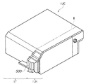
図12は、インクタンクと記録ヘッドとが一体的に形成されたヘッドカートリッジIJCの構成を示す外観斜視図である。図12において、点線KはインクタンクITと記録ヘッドIJHの境界線である。ヘッドカートリッジIJCにはこれがキャリッジ2に搭載されたときには、キャリッジ2側から供給される電気信号を受け取るための電極(不図示)が設けられている。そして、この電気信号によって、前述のように記録ヘッドIJHが駆動されてインクが吐出される。
FIG. 12 is an external perspective view showing a configuration of a head cartridge IJC in which an ink tank and a recording head are integrally formed. In FIG. 12, a dotted line K is a boundary line between the ink tank IT and the recording head IJH. The head cartridge IJC is provided with an electrode (not shown) for receiving an electric signal supplied from the
なお、図12において、500はインク吐出口列である。
In FIG. 12,
[実施例1]
図2に、実施例1を説明するための変換電圧発生部の回路図を示す。
[Example 1]
FIG. 2 shows a circuit diagram of a conversion voltage generator for explaining the first embodiment.
本実施例では先に説明した図6の構成中で変換電圧発生部の構成を変更している。 In the present embodiment, the configuration of the conversion voltage generator is changed in the configuration of FIG. 6 described above.
本発明における電圧発生回路である変換電圧発生部125は、外部より入力されるクロック(CLK)信号にシリアル信号である画像データ(DATA)を同期させ、DATA端子よりシフトレジスタS/Rに入力する。S/R101は、DATA端子より入力した前記シリアル信号をパラレルデータに変換し、イネーブル(ENB)信号に同期させてデジタルアナログコンバータ(DAC)部150へ出力する。DAC部150は、前記パラレルデータに応じた電圧VGを、出力段を構成するソースフォロアであるNMOSトランジスタ132のゲートへ印加する。
The conversion
前記パラレルデータに応じた電圧VGは、以下のように出力される。 The voltage VG corresponding to the parallel data is output as follows.
ここで、前記パラレルデータを構成する各ビットは、1つずつのヒータに対応した画像データを表している。そして、ビットが「0」であればその対応するヒータは駆動されず、「1」であればその対応するヒータは駆動されるものとする。 Here, each bit constituting the parallel data represents image data corresponding to one heater. If the bit is “0”, the corresponding heater is not driven, and if it is “1”, the corresponding heater is driven.
本実施例でのDAC部150は、S/R101から出力された画像データである前記パラレルデータを、前記パラレルデータによって、駆動される駆動素子数に対応する値が「1」となるビット数を判別し、この数に応じて電圧VGを出力する。このため、DAC部150は、前記パラレルデータを入力する不図示の入力バッファ、前記パラレルデータの駆動する駆動素子数に対応するビット数をカウントする不図示のカウンタを有する。さらに、DAC部150は、前記カウント結果に応じて出力する電圧VGを変更する不図示のスイッチを有する。ここで用いられる記録ヘッドが、複数の記録素子からなるブロック毎の時分割駆動を行う記録ヘッドである場合、さらに時分割のタイミングを指定するためのデコーダ(不図示)が設けられている。
In this embodiment, the
また、前記駆動する駆動素子数が多いほど、各駆動素子に入力される電圧の降下が大きくなるため、DAC部150は、前記駆動する駆動素子数が多いほど電圧VGを高くする。具体的には、例えば、DAC部150は、前記駆動する駆動素子数が多いほど電圧VGを高くなるように設定した、駆動する駆動素子数と電圧VGとの対応テーブルを備え、このテーブルに応じて対応する電圧VGを出力する。
Further, since the drop in the voltage input to each drive element increases as the number of drive elements to be driven increases, the
電圧VGがNMOSトランジスタ132のゲートへ印加されて生成されたドライバ駆動電圧VHTMは、NMOSトランジスタ132のソースから出力される。本構成により、ドライバ駆動電圧VHTMは、DAC部150からの出力電圧VGに応じて変化させることが可能となる。
The driver drive voltage VHTM generated by applying the voltage VG to the gate of the
本実施例では、VHTMを変更するためのデータとして、装置本体から送信される画像データそのものを用いている。 In this embodiment, the image data itself transmitted from the apparatus main body is used as data for changing the VHTM.
[実施例2]
図1は素子基板に作りこまれた本実施例の回路構成の概略構成を示すものである。
[Example 2]
FIG. 1 shows a schematic configuration of a circuit configuration of this embodiment built in an element substrate.
この図1は変換電圧発生部と記録ヘッドの素子基板に作りこまれた駆動回路や、画像データの選択回路との関係を示す図である。 FIG. 1 is a diagram showing the relationship between a conversion voltage generator and a drive circuit built in an element substrate of a recording head and an image data selection circuit.
本実施例のDAC100はカウンタ機能などを有しておらず、シフトレジスタに対して装置本体から画像データに続けて送信されるVHTM電圧設定データに応じてVHTM電圧を出力するものである。
The
図1に示すように、DAC100およびドライバトランジスタ駆動電圧出力部(ドライバ駆動電圧出力部)104からなる変換電圧発生部125が素子基板内に少なくとも1つ設けられる。なお、ドライバ駆動電圧出力部104は、NMOSトランジスタ132と抵抗とからなっている(図2参照)。
As shown in FIG. 1, at least one conversion
ここでVHTは、ヒータ電源電圧VHと等電位の電圧であり、記録装置本体から入力される。ドライバ駆動電圧VHTMは、変換電圧発生部125において、S/R101に入力される電圧設定信号を元に、ヒータ電源電圧VHと同電位の電圧VHTから生成される。
Here, VHT is a voltage having the same potential as the heater power supply voltage VH, and is input from the recording apparatus main body. The driver drive voltage VHTM is generated from the voltage VHT having the same potential as the heater power supply voltage VH based on the voltage setting signal input to the S /
生成されたドライバ駆動電圧VHTMは、ドライバ選択回路アレイ105へと供給される。ドライバ選択回路アレイ105は、別途S/R101に入力された画像データを元に、デコーダ102などの論理回路により所望の処理を行った後、所望のヒータに対応したビットを選択する。選択されたビットでは、ヒート時間を規定するHE信号が印加されている時間だけドライバ選択回路105からの出力を有効とし、ドライバ駆動電圧VHTMを該当するドライバトランジスタ123のゲートに印加する。ドライバ駆動電圧VHTMが印加されたドライバトランジスタ123は、直列に接続された電気熱変換素子であるヒータ124に電流を流し、ヒータ124での発熱、発泡を招き、インク吐出が行われる。
The generated driver drive voltage VHTM is supplied to the driver
図4にドライバ駆動電圧VHTMとドライバトランジスタの実効的な抵抗値の関係の一例を示す。 FIG. 4 shows an example of the relationship between the driver drive voltage VHTM and the effective resistance value of the driver transistor.
図4に示すように、ドライバ駆動電圧VHTMに応じて実効的な抵抗Ronが変化する。ヒータへ印加する電圧を高める場合、ドライバトランジスタ123の抵抗Ronを低くするようにドライバ駆動電圧VHTMを高く設定する。一方、ヒータへの印加電圧を抑制する場合、ドライバ駆動電圧VHTMを低く設定し、Ronを高くする。このドライバトランジスタ123の抵抗Ronの設定は、記録装置本体から画像データと共にドライバ駆動電圧VHTMを設定する信号を素子基板へ入力することで行う。これより、ヒートタイミング毎にドライバトランジスタ123の抵抗Ronを設定することが可能となる。
As shown in FIG. 4, the effective resistance Ron changes according to the driver drive voltage VHTM. When increasing the voltage applied to the heater, the driver drive voltage VHTM is set high so that the resistance Ron of the
本実施例では、先に述べたようにDAC100へ入力するデータとしては、シフトレジスタからVHTM設定データとして、オンするビット数(同じタイミングでヒータが駆動される数)を入力している。なおオンビット数に限らず、後述する実施例のように設定値であってもよいが、本実施例では装置本体側でカウントしたオンビット数に基づく設定値となっている。このオンビット数に応じてVHTMを制御し、オンビット数が多く電圧降下が大きいときはVHTMを高くすることでドライバトランジスタの実効的なオン抵抗を低くする。一方、オンビット数が少なく、電圧降下の影響が小さい時にはVHTMを低くすることでドライバトランジスタのオン抵抗を上げ、最適なヒータ駆動条件を得ることとしている。
In this embodiment, as described above, as data to be input to the
本実施例ではさらにオンビット数の情報に加え、以下に述べるような駆動セグメントに応じたVHTM制御を行うことも特徴としている。 In this embodiment, in addition to the information on the number of on-bits, the VHTM control corresponding to the drive segment as described below is performed.
図5に示す記録ヘッドのノズルアレイは、1セグメントごとに大、小の2種類の液滴サイズを吐出するものとしている。 The nozzle array of the recording head shown in FIG. 5 ejects two types of large and small droplet sizes for each segment.
なおここではノズルアレイ内で同時に大、小のノズルに対応したヒータが駆動されることはないような構成となっている。 Here, the heaters corresponding to the large and small nozzles are not driven simultaneously in the nozzle array.
図5は、変換電圧発生部と記録ヘッドの素子基板に設けられた駆動回路との関係を示す図である。この図を用いて後述する構成では、VHTMの変更は同時に駆動されるONビット数ではなく、吐出量の違いに対応したVHTM設定データでなされる。 FIG. 5 is a diagram illustrating a relationship between the conversion voltage generation unit and a drive circuit provided on the element substrate of the recording head. In the configuration to be described later with reference to this figure, the change of VHTM is made not by the number of ON bits driven simultaneously but by VHTM setting data corresponding to the difference in discharge amount.
図5で示した、奇数セグメント(seg)は、吐出するインク液滴が偶数segに対して大きな液滴となっている。奇数segに対応した大きな液滴を吐出するヒータを駆動するタイミングでは、ドライバ駆動電圧VHTMを高くし、ドライバトランジスタ123の実効的な抵抗値Ronを低下させヒータ124による発熱量を大きくする。また、偶数segに対応した小さな液滴を吐出するタイミングでは、ドライバ駆動電圧VHTMを低く設定し、Ronを高くすることでヒータ124による発熱量を小さくする。
In the odd-numbered segment (seg) shown in FIG. 5, the ejected ink droplets are larger than the even-numbered seg. At the timing of driving a heater that discharges large droplets corresponding to odd seg, the driver drive voltage VHTM is increased, the effective resistance value Ron of the
このように、吐出する液滴の大きさに応じて各ヒータによる発熱量を最適にすることで、最適な液滴サイズの吐出を各ノズルで実現できる。このことにより、異なる液滴サイズの吐出を同一の記録ヘッドで安定して実現でき、高速かつ高品位な記録が可能となる。 In this way, by optimizing the amount of heat generated by each heater according to the size of the droplet to be ejected, it is possible to achieve ejection with an optimum droplet size with each nozzle. As a result, ejection of different droplet sizes can be stably realized with the same recording head, and high-speed and high-quality recording is possible.
また、記録ヘッドやインクの温度が変化した場合、その変化量を別途不図示の温度モニタ手段により求め、記録ヘッドやインクの温度に応じた、各ヒータの発熱量の制御が可能となる。その結果、温度が変化した場合においても安定した発泡を実現でき、安定したインク吐出と高品位な記録画像を得ることができる。 Further, when the temperature of the recording head or ink changes, the amount of change is separately obtained by a temperature monitor means (not shown), and the amount of heat generated by each heater can be controlled according to the temperature of the recording head or ink. As a result, stable foaming can be realized even when the temperature changes, and stable ink ejection and a high-quality recorded image can be obtained.
さらに、ヒータ124やドライバトランジスタ123の製造バラツキなどに対しても、同様に、補正を行うことが可能となる。具体的には、テスト時や印字前にヘッドの製造バラツキを検出し、これを記録または記憶しておき、別途用意したバラツキに応じた補正テーブルに照らし合わせ、そのバラツキを補正する。この補正により、記録ヘッドの個体差によらない、安定したインク吐出、高品位記録が可能となる。
Furthermore, correction can be similarly performed for manufacturing variations of the
ここで、特に本実施例の特徴的な点は、電圧制御機能を素子基板内部に設けていることである。本構成をとることで、同様の効果を得るために外部電源電圧を制御する場合と比較し、高速な制御が可能となる。 Here, a characteristic point of this embodiment is that a voltage control function is provided inside the element substrate. By adopting this configuration, it becomes possible to perform high-speed control as compared with the case of controlling the external power supply voltage in order to obtain the same effect.
また、外部からの電源電圧を入力するラインには、瞬間的に数A程度の大きな電流を流す必要があるため、通常は数百μF以上の大きな容量を有するコンデンサを付加している。そのため、その電圧を変化させるために必要な時間が長くなり、数μ秒程度のヒータの駆動周期の間で、電圧を制御、安定化することが困難となる。 In addition, a capacitor having a large capacity of several hundred μF or more is usually added to a line for inputting an external power supply voltage because a large current of about several A must be instantaneously passed. For this reason, the time required to change the voltage becomes long, and it becomes difficult to control and stabilize the voltage during the heater driving cycle of about several microseconds.
しかし、本発明においては、ヘッド基板内部に設けたデジタルアナログコンバータによる電圧制御機能で電圧を変化させる。このため、デジタルアナログコンバータの応答速度を、ヒータの駆動周期に応じて設計することにより、外部での電源電圧制御と比較して、より高速な制御が可能となる。ここで制御する電圧は、ヒータに電流を流すためのヒータ電源電圧ではなく、ヒータの駆動を制御するドライバトランジスタのゲート電圧である。このドライバトランジスタのゲート電圧は、瞬間的に流れる電流は数mAから数十mA程度であることがほとんどであり、ヒータ電源から印加されるような大きな電圧である必要はない。そのため、高速な制御を実現可能となっている。 However, in the present invention, the voltage is changed by the voltage control function by the digital-analog converter provided in the head substrate. For this reason, by designing the response speed of the digital-analog converter in accordance with the driving cycle of the heater, it is possible to perform higher-speed control than external power supply voltage control. The voltage to be controlled here is not the heater power supply voltage for supplying a current to the heater but the gate voltage of the driver transistor that controls the driving of the heater. As for the gate voltage of this driver transistor, the current that flows instantaneously is almost several mA to several tens mA, and it is not necessary to be a large voltage applied from the heater power supply. Therefore, high-speed control can be realized.
このように、ドライバトランジスタのゲート電圧を高度に制御することで、ヒータの消費電力を制御可能となる。また、大液滴の吐出を行った直後のタイミングに電圧制御を行い、ついで小液滴の吐出を行い、さらにその直後に大液滴の吐出を行うといった駆動制御をすることにより制御の高速化も効果的に達成できる。また、本発明の構成は、記録ヘッドの温度制御なども可能とするものであり、理想的な吐出特性を実現し、高品位な記録を得ることが可能となる。 Thus, the power consumption of the heater can be controlled by highly controlling the gate voltage of the driver transistor. In addition, the voltage control is performed immediately after the large droplet is discharged, then the small droplet is discharged, and then the large droplet is discharged immediately thereafter. Can also be achieved effectively. Further, the configuration of the present invention enables the temperature control of the recording head and the like, realizing ideal ejection characteristics and obtaining high quality recording.
[実施例3]
図9は、実施例2を説明するための回路図である。
[Example 3]
FIG. 9 is a circuit diagram for explaining the second embodiment.
実施例2では、ヒートタイミング毎にドライバ駆動電圧VHTMの設定が可能となるよう、ヒートタイミング毎にドライバ駆動電圧VHTMを設定するためのデータをS/R101に画像データと共に入力していた。本実施例では、このドライバ駆動電圧VHTMを設定するためのデータを、外部より入力せず、基板上に配置した設定電圧メモリ140が保持していることを特徴としている。この設定電圧メモリ140に保持されているドライバ駆動電圧VHTMを設定するためのデータは、あらかじめ記録装置及び記録ヘッドの仕様または製造バラツキに応じて生成されている。
In the second embodiment, data for setting the driver drive voltage VHTM at each heat timing is input to the S /
本実施例の設定電圧メモリ140は、M0からM4の端子からの入力手段を有する5bitのメモリであり、このメモリを実施例1におけるS/R101の代替として用いている。この設定電圧メモリ140は、ドライバ駆動電圧VHTMが、素子基板の回路テスト時のヒータ抵抗及びドライバトランジスタの特性などの測定結果、本素子基板を用いる記録装置及び記録ヘッドの仕様等に応じた電圧となるように設定されたデータを保持する。
The set
異なる記録装置及び記録ヘッドに対応するようにドライバ駆動電圧VHTMの設定をすることにより、同一種類の素子基板を、異なる記録装置及び記録ヘッドの仕様に適応させることが可能となる。また、製造バラツキに伴う補正に応じたドライバ駆動電圧VHTMを設定するためのデータを、設定電圧メモリ140に保持させることにより、素子基板の製造歩留まりの向上も可能となる。
By setting the driver drive voltage VHTM so as to correspond to different recording apparatuses and recording heads, the same type of element substrate can be adapted to the specifications of different recording apparatuses and recording heads. Further, by holding data for setting the driver drive voltage VHTM corresponding to the correction accompanying the manufacturing variation in the setting
なお、本実施例では、設定電圧メモリ140として、ポリシリコン抵抗を用いたヒューズROMを用いているが、ポリシリコン抵抗を用いたヒューズROMに限らず、他の抵抗体を用いたヒューズROMまたは他の構成のメモリを用いることができる。
In this embodiment, a fuse ROM using a polysilicon resistor is used as the
また、本実施例では、設定電圧メモリ140を素子基板内に設けているが、素子基板外に設けても良い。例えば、記録ヘッドに別途EEPROMを設け、このEEPROMにドライバ駆動電圧VHTMを設定するためのデータを保持させることも可能である。
In this embodiment, the set
さらに、本実施例では、素子基板の回路テスト時に、設定電圧メモリ140にドライバ駆動電圧VHTMを設定するためのデータを保持させているが、例えば、記録装置本体に記録ヘッドを装着した状態で、前記データを保持させることも可能である。記録装置本体に記録ヘッドを装着し、実際に吐出特性を確認した上でドライバ駆動電圧VHTMを決定することも可能である。
Further, in the present embodiment, the data for setting the driver drive voltage VHTM is held in the setting
本実施例の構成をとることにより、製造バラツキのある記録ヘッドにおいても、安定した発泡が可能となり、安定した高品位な記録が可能な記録ヘッドを得ることができる。また、異なる記録装置及び記録ヘッド間で同一の素子基板を用いた場合などにおいても、各記録装置及び各記録ヘッドで最適なドライバ駆動電圧VHTMの設定が可能となり、安定した発泡による高品位な記録が可能となる。 By adopting the configuration of the present embodiment, even a recording head with manufacturing variations can be stably foamed, and a recording head capable of stable high-quality recording can be obtained. In addition, even when the same element substrate is used between different recording apparatuses and recording heads, it is possible to set an optimum driver driving voltage VHTM for each recording apparatus and each recording head, and high-quality recording by stable foaming. Is possible.
また、本発明に係る記録装置の形態として、コンピュータ等の情報処理機器の画像出力端末として一体または別体に設けられるものの他、リーダ等と組み合わせた複写装置、さらには送受信機能を有するファクシミリ装置の形態を取るものであっても良い。 Further, as a form of the recording apparatus according to the present invention, a copying apparatus combined with a reader or the like as well as a facsimile apparatus having a transmission / reception function in addition to an image output terminal of an information processing device such as a computer provided integrally or separately. It may take a form.
また、上記実施例はインクジェット記録ヘッド用の素子基板を例に説明したが、熱転写方式の記録ヘッド用、昇華型の記録ヘッド用等の素子基板に用いることが可能である。 In the above embodiment, the element substrate for the ink jet recording head has been described as an example. However, it can be used for an element substrate for a thermal transfer type recording head, a sublimation type recording head, or the like.
100 デジタルアナログコンバータ
104 ドライバトランジスタ駆動電圧出力部
121 レベル変換部
123 ドライバトランジスタ
124 ヒータ
125 変換電圧発生部
150 DAC部
100
Claims (5)
外部からシリアルに入力され、各ビットが前記複数のヒータの1つに対応したデジタル画像データを格納するシフトレジスタと、
ヒータ駆動信号を生成するヒータ選択回路と、
前記ヒータ駆動信号を昇圧して前記MOSトランジスタのゲートへ印加するレベル変換回路と、
前記シフトレジスタに格納されたデジタル画像データの各ビットがオンとなるビット数に応じた電圧を発生する電圧発生回路とを備え、
前記電圧発生回路は、前記発生した電圧をゲートに入力し、前記複数のヒータに印加される電圧と同電位の電圧をドレインに入力し、該ゲートに入力された電圧に従って、ソースからの出力電圧を変化させるNMOSトランジスタを含み、
前記レベル変換回路は、前記ソースからの出力電圧に従って、前記ヒータ駆動信号の昇圧を行うことを特徴とする素子基板。 An element substrate for a print head comprising a plurality of heaters and a plurality of MOS transistors provided corresponding to each of the plurality of heaters and switching driving of the heaters according to a voltage input to a gate. And
A shift register that is serially input from the outside and stores digital image data in which each bit corresponds to one of the plurality of heaters;
A heater selection circuit for generating a heater drive signal;
A level conversion circuit that boosts the heater drive signal and applies it to the gate of the MOS transistor;
And a voltage generating circuit that occurs voltages each bit of the digital image data stored in the shift register corresponding to the number of bits turned on,
The voltage generation circuit inputs the generated voltage to a gate, inputs a voltage having the same potential as the voltage applied to the plurality of heaters to a drain, and outputs an output voltage from a source according to the voltage input to the gate. Including an NMOS transistor that changes
The element substrate , wherein the level conversion circuit boosts the heater driving signal in accordance with an output voltage from the source .
Priority Applications (1)
| Application Number | Priority Date | Filing Date | Title |
|---|---|---|---|
| JP2006333861A JP5230093B2 (en) | 2006-12-11 | 2006-12-11 | Element substrate, recording head, recording apparatus |
Applications Claiming Priority (1)
| Application Number | Priority Date | Filing Date | Title |
|---|---|---|---|
| JP2006333861A JP5230093B2 (en) | 2006-12-11 | 2006-12-11 | Element substrate, recording head, recording apparatus |
Publications (3)
| Publication Number | Publication Date |
|---|---|
| JP2008143064A JP2008143064A (en) | 2008-06-26 |
| JP2008143064A5 JP2008143064A5 (en) | 2010-02-04 |
| JP5230093B2 true JP5230093B2 (en) | 2013-07-10 |
Family
ID=39603755
Family Applications (1)
| Application Number | Title | Priority Date | Filing Date |
|---|---|---|---|
| JP2006333861A Active JP5230093B2 (en) | 2006-12-11 | 2006-12-11 | Element substrate, recording head, recording apparatus |
Country Status (1)
| Country | Link |
|---|---|
| JP (1) | JP5230093B2 (en) |
Family Cites Families (6)
| Publication number | Priority date | Publication date | Assignee | Title |
|---|---|---|---|---|
| JP2001246751A (en) * | 2000-03-06 | 2001-09-11 | Canon Inc | Recording head, recording apparatus with the recording head, and method for driving recording head |
| JP2004188970A (en) * | 2002-11-25 | 2004-07-08 | Canon Inc | Recording equipment and controlling method for recording equipment |
| JP3997217B2 (en) * | 2003-06-10 | 2007-10-24 | キヤノン株式会社 | Inkjet recording head substrate, drive control method, inkjet recording head, and inkjet recording apparatus |
| JP2005111936A (en) * | 2003-10-10 | 2005-04-28 | Canon Inc | Recorder |
| JP4785375B2 (en) * | 2004-12-09 | 2011-10-05 | キヤノン株式会社 | Inkjet recording head substrate, recording head, head cartridge, and recording apparatus |
| JP2006212823A (en) * | 2005-02-01 | 2006-08-17 | Canon Inc | Recording apparatus and control method for recording head |
-
2006
- 2006-12-11 JP JP2006333861A patent/JP5230093B2/en active Active
Also Published As
| Publication number | Publication date |
|---|---|
| JP2008143064A (en) | 2008-06-26 |
Similar Documents
| Publication | Publication Date | Title |
|---|---|---|
| US6116714A (en) | Printing head, printing method and apparatus using same, and apparatus and method for correcting said printing head | |
| JP4989433B2 (en) | Head substrate, recording head, head cartridge, and recording apparatus | |
| EP1899163B1 (en) | Head substrate, printhead, head cartridge, and printing apparatus | |
| JP5064990B2 (en) | Recording head, head cartridge, recording apparatus | |
| JP5032964B2 (en) | Head substrate, recording head, head cartridge, and recording apparatus | |
| JPH07241992A (en) | Recording head, method and device for recording with such recording head | |
| JP4785375B2 (en) | Inkjet recording head substrate, recording head, head cartridge, and recording apparatus | |
| JP4546102B2 (en) | Recording head substrate, recording head using the recording head substrate, recording apparatus including the recording head, and head cartridge including the recording head | |
| JP5017202B2 (en) | Recording head and recording apparatus using the recording head | |
| JP4669278B2 (en) | Element substrate for recording head, recording head, and recording apparatus | |
| JP4799389B2 (en) | Head substrate, recording head, head cartridge, and recording apparatus | |
| KR20020083477A (en) | Printing apparatus and printing control method | |
| JP5230093B2 (en) | Element substrate, recording head, recording apparatus | |
| JP2009166257A (en) | Inkjet recording head, head cartridge and recording device | |
| JP4974664B2 (en) | RECORDING HEAD SUBSTRATE, RECORDING HEAD OR HEAD CARTRIDGE USING THE SUBSTRATE, AND RECORDING DEVICE USING THE RECORDING HEAD | |
| JP5451042B2 (en) | Recording head and recording apparatus | |
| JP3997217B2 (en) | Inkjet recording head substrate, drive control method, inkjet recording head, and inkjet recording apparatus | |
| JP2004306564A (en) | Substrate for recording head, recording head, temperature control method for recording head, and recording device | |
| JP4780882B2 (en) | Inkjet recording apparatus and inkjet recording method | |
| JP2006007761A (en) | Substrate for recording head, recording head, head cartridge and recorder | |
| JP5385586B2 (en) | Head substrate, recording head, head cartridge, and recording apparatus | |
| JP5166970B2 (en) | Element substrate for recording head and processing method thereof, recording head, and recording apparatus | |
| JP2009143017A (en) | Element substrate, recording head with this element substrate, head cartridge, and recorder | |
| JP2009056649A (en) | Recorder and recording control method therefor | |
| JP2005169866A (en) | Recording head and recording apparatus using it |
Legal Events
| Date | Code | Title | Description |
|---|---|---|---|
| A521 | Written amendment |
Effective date: 20091211 Free format text: JAPANESE INTERMEDIATE CODE: A523 |
|
| A621 | Written request for application examination |
Free format text: JAPANESE INTERMEDIATE CODE: A621 Effective date: 20091211 |
|
| A131 | Notification of reasons for refusal |
Effective date: 20110829 Free format text: JAPANESE INTERMEDIATE CODE: A131 |
|
| A521 | Written amendment |
Free format text: JAPANESE INTERMEDIATE CODE: A523 Effective date: 20111025 |
|
| A131 | Notification of reasons for refusal |
Free format text: JAPANESE INTERMEDIATE CODE: A131 Effective date: 20130108 |
|
| A521 | Written amendment |
Free format text: JAPANESE INTERMEDIATE CODE: A523 Effective date: 20130225 |
|
| TRDD | Decision of grant or rejection written | ||
| A01 | Written decision to grant a patent or to grant a registration (utility model) |
Effective date: 20130312 Free format text: JAPANESE INTERMEDIATE CODE: A01 |
|
| A61 | First payment of annual fees (during grant procedure) |
Free format text: JAPANESE INTERMEDIATE CODE: A61 Effective date: 20130319 |
|
| FPAY | Renewal fee payment (prs date is renewal date of database) |
Free format text: PAYMENT UNTIL: 20160329 Year of fee payment: 3 |