JP5032964B2 - Head substrate, recording head, head cartridge, and recording apparatus - Google Patents
Head substrate, recording head, head cartridge, and recording apparatus Download PDFInfo
- Publication number
- JP5032964B2 JP5032964B2 JP2007313953A JP2007313953A JP5032964B2 JP 5032964 B2 JP5032964 B2 JP 5032964B2 JP 2007313953 A JP2007313953 A JP 2007313953A JP 2007313953 A JP2007313953 A JP 2007313953A JP 5032964 B2 JP5032964 B2 JP 5032964B2
- Authority
- JP
- Japan
- Prior art keywords
- head
- recording
- ink
- voltage generation
- head substrate
- Prior art date
- Legal status (The legal status is an assumption and is not a legal conclusion. Google has not performed a legal analysis and makes no representation as to the accuracy of the status listed.)
- Active
Links
Images


Classifications
-
- B—PERFORMING OPERATIONS; TRANSPORTING
- B41—PRINTING; LINING MACHINES; TYPEWRITERS; STAMPS
- B41J—TYPEWRITERS; SELECTIVE PRINTING MECHANISMS, i.e. MECHANISMS PRINTING OTHERWISE THAN FROM A FORME; CORRECTION OF TYPOGRAPHICAL ERRORS
- B41J2/00—Typewriters or selective printing mechanisms characterised by the printing or marking process for which they are designed
- B41J2/005—Typewriters or selective printing mechanisms characterised by the printing or marking process for which they are designed characterised by bringing liquid or particles selectively into contact with a printing material
- B41J2/01—Ink jet
- B41J2/015—Ink jet characterised by the jet generation process
- B41J2/04—Ink jet characterised by the jet generation process generating single droplets or particles on demand
- B41J2/045—Ink jet characterised by the jet generation process generating single droplets or particles on demand by pressure, e.g. electromechanical transducers
- B41J2/04501—Control methods or devices therefor, e.g. driver circuits, control circuits
- B41J2/0458—Control methods or devices therefor, e.g. driver circuits, control circuits controlling heads based on heating elements forming bubbles
-
- B—PERFORMING OPERATIONS; TRANSPORTING
- B41—PRINTING; LINING MACHINES; TYPEWRITERS; STAMPS
- B41J—TYPEWRITERS; SELECTIVE PRINTING MECHANISMS, i.e. MECHANISMS PRINTING OTHERWISE THAN FROM A FORME; CORRECTION OF TYPOGRAPHICAL ERRORS
- B41J2/00—Typewriters or selective printing mechanisms characterised by the printing or marking process for which they are designed
- B41J2/005—Typewriters or selective printing mechanisms characterised by the printing or marking process for which they are designed characterised by bringing liquid or particles selectively into contact with a printing material
- B41J2/01—Ink jet
- B41J2/015—Ink jet characterised by the jet generation process
- B41J2/04—Ink jet characterised by the jet generation process generating single droplets or particles on demand
- B41J2/045—Ink jet characterised by the jet generation process generating single droplets or particles on demand by pressure, e.g. electromechanical transducers
- B41J2/04501—Control methods or devices therefor, e.g. driver circuits, control circuits
- B41J2/04508—Control methods or devices therefor, e.g. driver circuits, control circuits aiming at correcting other parameters
-
- B—PERFORMING OPERATIONS; TRANSPORTING
- B41—PRINTING; LINING MACHINES; TYPEWRITERS; STAMPS
- B41J—TYPEWRITERS; SELECTIVE PRINTING MECHANISMS, i.e. MECHANISMS PRINTING OTHERWISE THAN FROM A FORME; CORRECTION OF TYPOGRAPHICAL ERRORS
- B41J2/00—Typewriters or selective printing mechanisms characterised by the printing or marking process for which they are designed
- B41J2/005—Typewriters or selective printing mechanisms characterised by the printing or marking process for which they are designed characterised by bringing liquid or particles selectively into contact with a printing material
- B41J2/01—Ink jet
- B41J2/015—Ink jet characterised by the jet generation process
- B41J2/04—Ink jet characterised by the jet generation process generating single droplets or particles on demand
- B41J2/045—Ink jet characterised by the jet generation process generating single droplets or particles on demand by pressure, e.g. electromechanical transducers
- B41J2/04501—Control methods or devices therefor, e.g. driver circuits, control circuits
- B41J2/0452—Control methods or devices therefor, e.g. driver circuits, control circuits reducing demand in current or voltage
-
- B—PERFORMING OPERATIONS; TRANSPORTING
- B41—PRINTING; LINING MACHINES; TYPEWRITERS; STAMPS
- B41J—TYPEWRITERS; SELECTIVE PRINTING MECHANISMS, i.e. MECHANISMS PRINTING OTHERWISE THAN FROM A FORME; CORRECTION OF TYPOGRAPHICAL ERRORS
- B41J2/00—Typewriters or selective printing mechanisms characterised by the printing or marking process for which they are designed
- B41J2/005—Typewriters or selective printing mechanisms characterised by the printing or marking process for which they are designed characterised by bringing liquid or particles selectively into contact with a printing material
- B41J2/01—Ink jet
- B41J2/015—Ink jet characterised by the jet generation process
- B41J2/04—Ink jet characterised by the jet generation process generating single droplets or particles on demand
- B41J2/045—Ink jet characterised by the jet generation process generating single droplets or particles on demand by pressure, e.g. electromechanical transducers
- B41J2/04501—Control methods or devices therefor, e.g. driver circuits, control circuits
- B41J2/04541—Specific driving circuit
-
- B—PERFORMING OPERATIONS; TRANSPORTING
- B41—PRINTING; LINING MACHINES; TYPEWRITERS; STAMPS
- B41J—TYPEWRITERS; SELECTIVE PRINTING MECHANISMS, i.e. MECHANISMS PRINTING OTHERWISE THAN FROM A FORME; CORRECTION OF TYPOGRAPHICAL ERRORS
- B41J2/00—Typewriters or selective printing mechanisms characterised by the printing or marking process for which they are designed
- B41J2/005—Typewriters or selective printing mechanisms characterised by the printing or marking process for which they are designed characterised by bringing liquid or particles selectively into contact with a printing material
- B41J2/01—Ink jet
- B41J2/015—Ink jet characterised by the jet generation process
- B41J2/04—Ink jet characterised by the jet generation process generating single droplets or particles on demand
- B41J2/045—Ink jet characterised by the jet generation process generating single droplets or particles on demand by pressure, e.g. electromechanical transducers
- B41J2/04501—Control methods or devices therefor, e.g. driver circuits, control circuits
- B41J2/04548—Details of power line section of control circuit
-
- B—PERFORMING OPERATIONS; TRANSPORTING
- B41—PRINTING; LINING MACHINES; TYPEWRITERS; STAMPS
- B41J—TYPEWRITERS; SELECTIVE PRINTING MECHANISMS, i.e. MECHANISMS PRINTING OTHERWISE THAN FROM A FORME; CORRECTION OF TYPOGRAPHICAL ERRORS
- B41J2/00—Typewriters or selective printing mechanisms characterised by the printing or marking process for which they are designed
- B41J2/005—Typewriters or selective printing mechanisms characterised by the printing or marking process for which they are designed characterised by bringing liquid or particles selectively into contact with a printing material
- B41J2/01—Ink jet
- B41J2/015—Ink jet characterised by the jet generation process
- B41J2/04—Ink jet characterised by the jet generation process generating single droplets or particles on demand
- B41J2/045—Ink jet characterised by the jet generation process generating single droplets or particles on demand by pressure, e.g. electromechanical transducers
- B41J2/04501—Control methods or devices therefor, e.g. driver circuits, control circuits
- B41J2/0455—Details of switching sections of circuit, e.g. transistors
-
- B—PERFORMING OPERATIONS; TRANSPORTING
- B41—PRINTING; LINING MACHINES; TYPEWRITERS; STAMPS
- B41J—TYPEWRITERS; SELECTIVE PRINTING MECHANISMS, i.e. MECHANISMS PRINTING OTHERWISE THAN FROM A FORME; CORRECTION OF TYPOGRAPHICAL ERRORS
- B41J2/00—Typewriters or selective printing mechanisms characterised by the printing or marking process for which they are designed
- B41J2/005—Typewriters or selective printing mechanisms characterised by the printing or marking process for which they are designed characterised by bringing liquid or particles selectively into contact with a printing material
- B41J2/01—Ink jet
- B41J2/015—Ink jet characterised by the jet generation process
- B41J2/04—Ink jet characterised by the jet generation process generating single droplets or particles on demand
- B41J2/045—Ink jet characterised by the jet generation process generating single droplets or particles on demand by pressure, e.g. electromechanical transducers
- B41J2/04501—Control methods or devices therefor, e.g. driver circuits, control circuits
- B41J2/04563—Control methods or devices therefor, e.g. driver circuits, control circuits detecting head temperature; Ink temperature
-
- B—PERFORMING OPERATIONS; TRANSPORTING
- B41—PRINTING; LINING MACHINES; TYPEWRITERS; STAMPS
- B41J—TYPEWRITERS; SELECTIVE PRINTING MECHANISMS, i.e. MECHANISMS PRINTING OTHERWISE THAN FROM A FORME; CORRECTION OF TYPOGRAPHICAL ERRORS
- B41J2/00—Typewriters or selective printing mechanisms characterised by the printing or marking process for which they are designed
- B41J2/005—Typewriters or selective printing mechanisms characterised by the printing or marking process for which they are designed characterised by bringing liquid or particles selectively into contact with a printing material
- B41J2/01—Ink jet
- B41J2/135—Nozzles
- B41J2/14—Structure thereof only for on-demand ink jet heads
- B41J2/14016—Structure of bubble jet print heads
- B41J2/14072—Electrical connections, e.g. details on electrodes, connecting the chip to the outside...
Description
本発明はヘッド基板、記録ヘッド、ヘッドカートリッジ、及び記録装置に関する。本発明は、特に、記録に必要な熱エネルギーを発生する電気熱変換素子とそれを駆動する駆動回路を同一基板上に形成したヘッド基板、そのヘッド基板を用いた記録ヘッド、その記録ヘッドを用いたヘッドカートリッジ、及び記録装置に関するものである。 The present invention relates to a head substrate, a recording head, a head cartridge, and a recording apparatus. In particular, the present invention uses a head substrate in which an electrothermal conversion element that generates thermal energy necessary for recording and a drive circuit for driving the same are formed on the same substrate, a recording head using the head substrate, and the recording head. The present invention relates to a conventional head cartridge and a recording apparatus.
従来のインクジェット記録ヘッド(以下、記録ヘッド)の電気熱変換素子(ヒータ)とその駆動回路は、例えば、特許文献1に示されているように半導体プロセス技術を用いて同一基板上に形成されている。
An electrothermal transducer (heater) of a conventional ink jet recording head (hereinafter referred to as a recording head) and its drive circuit are formed on the same substrate by using a semiconductor process technique as disclosed in
さて、近年の記録ヘッドは記録の高速化、高画質化が進んでおり、配列するセグメント数が増加している。また、多くの数のセグメントを高速駆動することにより消費電力が増加してきている。その結果、記録ヘッドの昇温が問題となっている。記録ヘッドの昇温はインクの吐出不良や吐出インク量のばらつきを招き、記録画質の低下の原因となるからである。 Now, with recent recording heads, the recording speed and image quality are increasing, and the number of segments arranged is increasing. In addition, power consumption has been increased by driving a large number of segments at high speed. As a result, the temperature rise of the recording head is a problem. This is because the temperature rise of the recording head causes ink ejection failure and variation in the amount of ejected ink, which causes a decrease in recording image quality.
記録ヘッドを構成する要素の内、電力消費が大きい部分として、インクを加熱するヒータ部の他に変換電圧発生回路がある。変換電圧発生回路は駆動回路と共通の基板に少なくとも1つは設けられている。加えて、カラー記録のために複数のインクを吐出するため、1つのヘッド基板にその複数インクに対応して複数の回路が構成されている場合、同じ基板内に複数の変換電圧発生回路が設けられていることが多い。このような変換電圧発生回路の増加は電力消費増加の原因となる。 Among the elements constituting the recording head, as a portion that consumes a large amount of power, there is a conversion voltage generation circuit in addition to a heater unit that heats ink. At least one conversion voltage generation circuit is provided on a common substrate with the drive circuit. In addition, in order to eject a plurality of inks for color recording, when a plurality of circuits are configured on one head substrate corresponding to the plurality of inks, a plurality of conversion voltage generation circuits are provided on the same substrate. It is often done. Such an increase in the conversion voltage generation circuit causes an increase in power consumption.
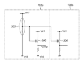
図11は従来の変換電圧発生回路の一例とその周辺回路図を示す図である。 FIG. 11 is a diagram showing an example of a conventional conversion voltage generation circuit and its peripheral circuit diagram.
図11の変換電圧発生回路300を除く部分は1セグメント分の等価回路を示した図である。変換電圧発生回路300より出力される変換電圧(VHTM)は複数セグメントの昇圧回路307で共通に使われる。昇圧回路307はシフトレジスタなどのロジック回路を動作させるためのロジック電源電圧(例えば、3.3V)の信号を変換電圧(VHTM)の信号に昇圧する回路である。昇圧回路307からの出力電圧はスイッチング素子(駆動素子)305であるMOS−FETのゲートに印加される。スイッチング素子305にはヒータ304が直列に接続される。変換電圧発生回路300はヒータに印加される電圧である24V程度のヒータ電圧(VH)と同じ電圧(VHT)を電源としており、その回路はポリシリコンや拡散抵抗を含む抵抗素子やMOSFET306からなっている。
The portion excluding the conversion
変換電圧発生回路はソースホロア回路の形態をとっており、MOSFET306のゲートに一定の基準電圧を印加することで、変換電圧(VHTM)の値が規定される。また、MOSFET306のゲートに常に一定の電圧が印加されているので、MOSFET306のドレインソース間に一斉に電流が流れても変換電位が変動しづらいような回路構成となっている。この変換電位を常に一定に保つためには、MOSFET306のゲートに常に一定の電圧がかかるようにしなくてはならない。
The conversion voltage generation circuit takes the form of a source follower circuit, and the value of the conversion voltage (VHTM) is defined by applying a constant reference voltage to the gate of the
そこで、基準電圧発生部303の一例として図11では分圧抵抗によって一定の基準電圧を発生させている。その抵抗素子としては、熱により抵抗値変動が起こりづらい素子(例えば、ポリシリコン)が望ましい。
しかしながら、このような回路構成では基準電圧発生部には常に貫通電流が流れているため消費電力が大きくなる。 However, in such a circuit configuration, since a through current always flows through the reference voltage generator, power consumption increases.
また、分圧抵抗に使う抵抗素子が問題となる。半導体に用いる抵抗素子としては、レイアウト面積の小さい拡散抵抗が一般的であるが、拡散抵抗はバイアス電圧に依存して変化するため、分圧抵抗に用いる素子としては理想的であるとは言えない。そのため、上記従来例では、バイアス電圧に依存しない抵抗体である金属抵抗やポリシリコンを用いることがある。しかしながら、このような抵抗体を用いるとヘッド基板のレイアウト面積が大きくなり、チップサイズが大きくなる。これは、ヘッド基板の製造コストアップとなってしまう。 In addition, a resistance element used for the voltage dividing resistor becomes a problem. As a resistance element used for a semiconductor, a diffusion resistor having a small layout area is generally used. However, since the diffusion resistance changes depending on a bias voltage, it is not ideal as an element used for a voltage dividing resistor. . Therefore, in the above conventional example, a metal resistor or polysilicon which is a resistor independent of the bias voltage may be used. However, when such a resistor is used, the layout area of the head substrate increases and the chip size increases. This increases the manufacturing cost of the head substrate.
本発明は上記従来例に鑑みてなされたもので、低コストで電力損失が少なく、さらに高集積化もしくは小型化が可能なヘッド基板を提供することを目的としている。また、そのヘッド基板を用いた記録ヘッド、ヘッドカートリッジ、及び記録装置を提供することも目的としている。 The present invention has been made in view of the above conventional example, and an object thereof is to provide a head substrate that is low in cost, has little power loss, and can be highly integrated or downsized. Another object of the present invention is to provide a recording head, a head cartridge, and a recording apparatus using the head substrate.
上記目的を達成するために本発明のヘッド基板は、以下のような構成からなる。 In order to achieve the above object, the head substrate of the present invention has the following configuration.
即ち、ヘッド基板であって、複数の記録素子と、前記複数の記録素子を駆動する複数の駆動素子と、前記複数の駆動素子を駆動するための駆動信号の電圧を昇圧する複数の昇圧回路と、前記複数の昇圧回路を複数のグループに分割し、各グループに属する昇圧回路に共通の電圧を供給する、グループに対応して設けられた複数の変換電圧発生回路とを有し、前記複数の変換電圧発生回路は、前記複数の変換電圧発生回路で発生する電圧値を規定するための基準電圧を発生する、抵抗体で構成される基準電圧発生部を共有する構成であることを特徴とする。 That is, the head substrate includes a plurality of recording elements, a plurality of driving elements for driving the plurality of recording elements, and a plurality of boosting circuits for boosting a voltage of a driving signal for driving the plurality of driving elements, The plurality of booster circuits are divided into a plurality of groups, and supply a common voltage to the booster circuits belonging to each group. The conversion voltage generation circuit is configured to share a reference voltage generation unit configured of a resistor that generates a reference voltage for defining a voltage value generated by the plurality of conversion voltage generation circuits. .
また他の発明によれば、上記構成のヘッド基板を用いた記録ヘッドを備える。 According to another invention, a recording head using the head substrate having the above-described configuration is provided.
さらに他の発明によれば、上記記録ヘッドとその記録ヘッドに供給するインクを収容したインクタンクとを一体化したヘッドカートリッジを備える。 According to another aspect of the invention, a head cartridge is provided in which the recording head and an ink tank that stores ink to be supplied to the recording head are integrated.
またさらに他の発明によれば、上記記録ヘッド又はヘッドカートリッジを搭載した記録装置を備える。 According to still another aspect of the invention, a recording apparatus including the recording head or the head cartridge is provided.
従って本発明によれば、1つの基準電圧発生部を複数の変換電圧発生回路で共有するので、消費電力の大きい基準電圧発生部の数を削減でき、消費電力を低減することができる。また、消費電力の低減により、記録ヘッドの昇温を抑制でき、それによる画質品位の低下を抑制することに貢献する。 Therefore, according to the present invention, since one reference voltage generator is shared by a plurality of conversion voltage generators, the number of reference voltage generators with large power consumption can be reduced, and power consumption can be reduced. Further, the power consumption can be reduced, so that the temperature rise of the recording head can be suppressed, thereby contributing to the suppression of the deterioration in image quality.
また、基準電圧発生部を構成する抵抗は従来よりヘッド基板上で大きなレイアウト面積を占めていたので、基準電圧発生部の削減はヘッド基板面積の削減に貢献することになる。これにより、ヘッド基板の小型化やそれによる生産コストの削減も可能となる。 In addition, since the resistors constituting the reference voltage generating unit occupy a larger layout area on the head substrate than before, the reduction of the reference voltage generating unit contributes to the reduction of the head substrate area. As a result, it is possible to reduce the size of the head substrate and thereby reduce the production cost.
以下添付図面を参照して本発明の好適な実施例について、さらに具体的かつ詳細に説明する。なお、既に説明した部分には同一符号を付し重複説明を省略する。 Hereinafter, preferred embodiments of the present invention will be described more specifically and in detail with reference to the accompanying drawings. In addition, the same code | symbol is attached | subjected to the already demonstrated part and duplication description is abbreviate | omitted.
なお、この明細書において、「記録」(「プリント」という場合もある)とは、文字、図形等有意の情報を形成する場合のみならず、有意無意を問わない。また人間が視覚で知覚し得るように顕在化したものであるか否かを問わず、広く記録媒体上に画像、模様、パターン等を形成する、または媒体の加工を行う場合も表すものとする。 In this specification, “recording” (sometimes referred to as “printing”) is not limited to the case of forming significant information such as characters and graphics, but may be significant. It also represents the case where an image, a pattern, a pattern, etc. are widely formed on a recording medium, or the medium is processed, regardless of whether it is manifested so that humans can perceive it visually. .
また、「記録媒体」とは、一般的な記録装置で用いられる紙のみならず、広く、布、プラスチック・フィルム、金属板、ガラス、セラミックス、木材、皮革等、インクを受容可能なものも表すものとする。 “Recording medium” refers not only to paper used in general recording apparatuses but also widely to cloth, plastic film, metal plate, glass, ceramics, wood, leather, and the like that can accept ink. Shall.
さらに、「インク」(「液体」と言う場合もある)とは、上記「記録(プリント)」の定義と同様広く解釈されるべきものである。従って、記録媒体上に付与されることによって、画像、模様、パターン等の形成または記録媒体の加工、或いはインクの処理(例えば記録媒体に付与されるインク中の色剤の凝固または不溶化)に供され得る液体を表すものとする。 Further, “ink” (sometimes referred to as “liquid”) should be interpreted widely as in the definition of “recording (printing)”. Therefore, by being applied on the recording medium, it is used for formation of images, patterns, patterns, etc., processing of the recording medium, or ink processing (for example, solidification or insolubilization of the colorant in the ink applied to the recording medium). It shall represent a liquid that can be made.
またさらに、記録要素とは、特にことわらない限り吐出口ないしこれに連通する液路およびインク吐出に利用されるエネルギーを発生する素子(記録素子)を総括して言うものとする。 Furthermore, unless otherwise specified, the recording element is a generic term for an ejection port or a liquid path communicating with the ejection port and an element (recording element) that generates energy used for ink ejection.
以下に用いる記録ヘッド用基板(ヘッド基板)とは、シリコン半導体からなる単なる基体を指し示すものではなく、その基板上に各素子や配線等が設けられた構成を差し示すものである。 The recording head substrate (head substrate) used below does not indicate a simple substrate made of a silicon semiconductor, but indicates a configuration in which elements, wirings, and the like are provided on the substrate.
さらに、基板上とは、単に素子基板の上を指し示すだけでなく、素子基板の表面、表面近傍の素子基板内部側をも示すものである。また、本発明でいう「作り込み」とは、別体の各素子を単に基体表面上に別体として配置することを指し示している言葉ではなく、各素子を半導体回路の製造工程等によって素子板上に一体的に形成、製造することを示すものである。 Further, the term “on the substrate” means not only the element substrate but also the surface of the element substrate and the inside of the element substrate near the surface. The term “built-in” as used in the present invention is not a word indicating that each separate element is simply arranged separately on the surface of the substrate. It shows that it is integrally formed and manufactured on top.
始めに、以下で説明する本発明に従う記録ヘッドを用いる記録装置の代表的な全体構成および制御構成について説明する。 First, a representative overall configuration and control configuration of a recording apparatus using a recording head according to the present invention described below will be described.
<インクジェット記録装置の説明(図1)>
図1は本発明の代表的な実施例であるインクジェット記録装置1の構成の概要を示す外観斜視図である。
<Description of Inkjet Recording Apparatus (FIG. 1)>
FIG. 1 is an external perspective view showing an outline of the configuration of an ink
図1に示すように、インクジェット記録装置(以下、記録装置という)は、インクジェット方式に従ってインクを吐出して記録を行なう記録ヘッド3をキャリッジ2に搭載し、キャリッジ2を矢印A方向に往復移動させて記録を行う。記録紙などの記録媒体Pを給紙機構5を介して給紙し、記録位置まで搬送し、その記録位置において記録ヘッド3から記録媒体Pにインクを吐出することで記録を行なう。
As shown in FIG. 1, an ink jet recording apparatus (hereinafter referred to as a recording apparatus) includes a
記録装置1のキャリッジ2には記録ヘッド3を搭載するのみならず、記録ヘッド3に供給するインクを貯留するインクカートリッジ6を装着する。インクカートリッジ6はキャリッジ2に対して着脱自在になっている。
In addition to mounting the
図1に示した記録装置1はカラー記録が可能であり、そのためにキャリッジ2にはマゼンタ(M)、シアン(C)、イエロ(Y)、ブラック(K)のインクを夫々、収容した4つのインクカートリッジを搭載している。これら4つのインクカートリッジは夫々独立に着脱可能である。
The
この実施例の記録ヘッド3は、熱エネルギーを利用してインクを吐出するインクジェット方式を採用している。このため、記録ヘッド3には記録素子として熱エネルギーを発生するために電気熱変換体を備えている。この電気熱変換体は各吐出口のそれぞれに対応して設けられ、記録信号に応じて対応する電気熱変換体にパルス電圧を印加することによって対応する吐出口からインクを吐出する。
The
<インクジェット記録装置の制御構成(図2)>
図2は図1に示した記録装置の制御構成を示すブロック図である。
<Control Configuration of Inkjet Recording Apparatus (FIG. 2)>
FIG. 2 is a block diagram showing a control configuration of the recording apparatus shown in FIG.
図2に示すように、コントローラ600は、MPU601、ROM602、特殊用途集積回路(ASIC)603、RAM604、システムバス605、A/D変換器606などで構成される。ここで、ROM602は後述する制御シーケンスに対応したプログラム、所要のテーブル、その他の固定データを格納する。ASIC603は、キャリッジモータM1の制御、搬送モータM2の制御、及び、記録ヘッド3の制御のための制御信号を生成する。RAM604は、画像データの展開領域やプログラム実行のための作業用領域等として用いられる。システムバス605は、MPU601、ASIC603、RAM604を相互に接続してデータの授受を行う。A/D変換器606は以下に説明するセンサ群からのアナログ信号を入力してA/D変換し、デジタル信号をMPU601に供給する。
As shown in FIG. 2, the
また、図2において、610は画像データの供給源となるコンピュータ(或いは、画像読取り用のリーダやデジタルカメラなど)でありホスト装置と総称される。ホスト装置610と記録装置1との間ではインタフェース(I/F)611を介して画像データ、コマンド、ステータス信号等を送受信する。この画像データは、例えば、ラスタ形式で入力される。
In FIG. 2,
さらに、620はスイッチ群であり、電源スイッチ621、プリントスイッチ622、回復スイッチ623などから構成される。
630は装置状態を検出するためのセンサ群であり、位置センサ631、温度センサ632等から構成される。
さらに、640はキャリッジ2を矢印A方向に往復走査させるためのキャリッジモータM1を駆動させるキャリッジモータドライバ、642は記録媒体Pを搬送するための搬送モータM2を駆動させる搬送モータドライバである。644は記録ヘッド3を駆動させるヘッドドライバである。
Further, 640 is a carriage motor driver that drives a carriage motor M1 for reciprocating scanning of the
ASIC603は、記録ヘッド3による記録走査の際に、RAM604の記憶領域に直接アクセスしながら記録ヘッドに対して記録素子(ヒータ)の記録信号(DATA)を転送する。加えて、ヘッドドライバ644を介して、MPU601やASIC603からの制御信号を記録ヘッド3に供給する。また、電源部(不図示)からの電力も記録ヘッド3に供給される。
The
図3は記録ヘッドとインクカートリッジとで構成される記録ヘッドカートリッジ1000の概観を示す斜視図である。
FIG. 3 is a perspective view showing an overview of a
図3の(a)と(b)から分かるように、記録ヘッドカートリッジ1000は4つのインクカートリッジ6と記録ヘッド3とから構成されており、互いに対して分離可能である。図3の(a)が4つのインクカートリッジ6と記録ヘッド3に装着した様子を示し、図3の(b)が記録ヘッド3から4つのインクカートリッジ6が分離した様子を示している。
As can be seen from FIGS. 3A and 3B, the
また、インクカートリッジ6はイエロ(Y)インク、シアン(C)インク、マゼンタ(M)インク、ブラック(K)インクを夫々収容する4つのインクカートリッジ6Y、6C、6M、6Kから構成されている。これらのインクカートリッジは中のインクがなくなると、夫々個別的に記録ヘッドから分離して交換できる。
The
記録ヘッドカートリッジ1000は記録装置本体に設けられたキャリッジ2の位置決め手段および電気的接点によって固定支持されるとともに、キャリッジ2に対して着脱可能となっている。
The
また、記録ヘッド3は、電気信号に応じて膜沸騰をインクに対して生じさせるための熱エネルギーを生成するヒータを用いて記録を行う方式の記録ヘッドであって、ヒータ面に対向する側にインクを吐出する、所謂、サイドシュータ型の記録ヘッドである。
The
図4は記録ヘッド3の詳細な構成を示す分解斜視図である。
FIG. 4 is an exploded perspective view showing a detailed configuration of the
図4に示すように、記録ヘッド3は記録素子ユニット1002と、インク供給ユニット1003と、4つのインクカートリッジを受容するタンクホルダ2000とから構成されている。記録素子ユニット1002は複数の発熱抵抗体(ヒータ)を実装したヘッド基板1100C(後述)とヘッド基板1100K(後述)を持つ。なお、記録素子ユニット1002のインク連通口(不図示)とインク供給ユニット1003のインク連通口2301とをインクがリークしないように連通させるため、各部材を圧着するようジョイントシール部材2300を介してビス2400で固定している。
As shown in FIG. 4, the
また、上述のように、インクカートリッジ6と記録ヘッド3と分離可能に構成しても良いが、これらが一体的に形成されて交換可能なヘッドカートリッジIJCを構成しても良い。
Further, as described above, the
図5は、インクタンクと記録ヘッドとが一体化されたヘッドカートリッジIJCの構成を示す外観斜視図である。図5において、点線KはインクタンクITと記録ヘッドIJHの境界線である。ヘッドカートリッジIJCにはこれがキャリッジ2に搭載されたときには、キャリッジ2側から供給される電気信号を受け取るための電極(不図示)が設けられており、この電気信号によって、前述のように記録ヘッドIJHが駆動されてインクが吐出される。
FIG. 5 is an external perspective view showing a configuration of a head cartridge IJC in which an ink tank and a recording head are integrated. In FIG. 5, a dotted line K is a boundary line between the ink tank IT and the recording head IJH. The head cartridge IJC is provided with an electrode (not shown) for receiving an electrical signal supplied from the
なお、図5において、500はインク吐出口列である。
In FIG. 5,
以下、上記の構成の記録装置に搭載される記録ヘッドのヘッド基板の実施例について説明する。 Hereinafter, examples of the head substrate of the recording head mounted on the recording apparatus having the above-described configuration will be described.
なお、図4ではカラーインク吐出に用いるために3つのインク供給口を備えたヘッド基板とブラックインク吐出に用いるために1つのインク供給口を備えたヘッド基板とを総称してヘッド基板として言及した。しかしながら、以下の説明では、1つのインク供給口を備えたヘッド基板を1100K、3つのインク供給口を備えたヘッド基板を1100Cとして個別に言及する。 In FIG. 4, a head substrate having three ink supply ports for use in color ink discharge and a head substrate having one ink supply port for use in black ink discharge are collectively referred to as a head substrate. . However, in the following description, the head substrate having one ink supply port is individually referred to as 1100K, and the head substrate having three ink supply ports is individually referred to as 1100C.
図6はヒータと駆動回路が同一基板上に作り込まれることで一体形成されているヘッド基板1100Kのレイアウト構造を示す平面図である。
FIG. 6 is a plan view showing a layout structure of a
図6に示すように、ヘッド基板1100Kには、厚さ0.5〜1mmのSi基板の片面の矩形状の細長いインク供給口101を挟んだ両側にその長手方向に、インクを吐出するための複数のヒータからなるヒータアレイ102が設けられる。さらに、これに対応する複数のインク流路(不図示)と複数のインク吐出口(不図示)とがフォトリソグラフィ技術により形成される。インク供給口101にはヘッド基板の外部(即ち、インクタンク或いはインクカートリッジ)よりインクが供給される。
As shown in FIG. 6, the
さらに、ヘッド基板1100Kにはヒータアレイ102を構成する各ヒータの駆動に必要なドライバトランジスタ(前述の駆動素子に相当)103、昇圧回路104、AND回路などのヒータ選択回路105がヒータアレイ102に沿った方向に配置されている。また、シフトレジスタ107、デコーダ106、及びパッド109がヘッド基板1100Kの上下端部に配置されている。なお、ここでいう上下端部とは図面の紙面上における上端部と下端部のことを意味する。さらに、図6から分かるように、ヘッド基板1100Kの上端部に近接して配置された2つの変換電圧発生回路108a、108bは、インク供給口101を挟んで配置された2つのヒータアレイ102夫々に対応した昇圧回路104の電源を供給している。ここでいう上端部とは、図面の紙面上における上端部を指す。
Further, on the
なお、図6に示すヘッド基板1100Kには複数の電極パッドが示されており、これらを総称する参照番号として109を用いている。
A plurality of electrode pads are shown on the
さて、記録信号や制御信号はパッド109から入力されシフトレジスタ107、デコーダ106に入力される。その後、それぞれの回路より出力された信号はシフトレジスタやシフトレジスタに対応して設けられたラッチ(不図示)からの信号とデコーダ106からの信号との論理積を取るAND回路などで構成されたヒータ選択回路105に入力る。そしてヒータ選択回路105からのヒータ選択信号(駆動信号)によって最終的に駆動電流を流すべきヒータを選択する。
Recording signals and control signals are input from the
ヒータ選択回路105より出力されたヒータ選択信号によりドライバトランジスタ103を駆動するため、昇圧回路104によりヒータ選択信号の電圧レベルを昇圧する。昇圧された後の信号の電圧はドライバトランジスタ103を駆動できる程度の電圧であり、その値はシフトレジスタ等を駆動するための制御電圧や記録信号のロジック電圧よりも高く、かつドライバトランジスタや昇圧回路を構成する素子の耐圧よりも低い。また、その電圧を発生するのが変換電圧発生回路108a、108bである。
In order to drive the
昇圧されたヒータ選択信号によりドライバトランジスタ(駆動素子)103が駆動し、ヒータアレイ102の所望のヒータに電流が流れ、そのヒータの発熱によりインクが沸騰し、その圧力によりインクが吐出される。
The driver transistor (driving element) 103 is driven by the boosted heater selection signal, a current flows to a desired heater of the
図7はヘッド基板1100Kに形成される変換電圧発生回路108a、108bの等価回路を示す図である。なお、図7において、既に図11で説明したのと同じ構成要素や電圧については同じ参照番号、参考記号を付し、その説明は省略する。
FIG. 7 is a diagram showing an equivalent circuit of the conversion
図7に示す回路構成によれば、図11に示すように従来は各変換電圧発生回路に設けられていた基準電圧発生部303を2つの変換電圧発生回路108a、108bで共有する。こうすることで、消費電力の多い貫通電流が流れる基準電圧発生部303を1つ削減することができ、消費電力の低減が実現できる。従来と同じ貫通電流値の(分圧抵抗値を変えない)場合、その電力消費は従来の半分となる。また、消費電力低減により、記録画質劣化の原因となる記録ヘッドの昇温も抑制することが可能となる。
According to the circuit configuration shown in FIG. 7, as shown in FIG. 11, the reference
また、この実施例では、基準電圧発生部303の素子として温度変化による抵抗値変動は小さいがレイアウト面積の大きいポリシリコン抵抗を用いている。この場合であっても、基準電圧発生部303の共通化により必要な抵抗素子数が半分になる。このため、そのレイアウト面積を半分にすることができる。これにより、1ヘッド基板当たりのヒータ数を増加させたり、他の回路を実装することが可能となる。また、ヘッド基板面積の削減も実現できるので、チップコストも低く抑えることが可能となる。
In this embodiment, a polysilicon resistor having a small layout area but a large layout area is used as an element of the
基準電圧発生部303の素子としては、ポリシリコンの抵抗以外の抵抗でも良いが、前述のようにバイアス電圧に依存しない点でポリシリコンを使用することが望ましい。
As an element of the reference
図8はヒータと駆動回路が同一基板上に一体形成されているヘッド基板1100Cのレイアウト構造を示す平面図である。
FIG. 8 is a plan view showing a layout structure of a
ヘッド基板1100Cは一つの基板上に3つのインク供給口401C、401M、401Yを備えている。そして、それらインク供給口各々の両側に、インク供給口に沿ってヒータアレイとドライバトランジスタと昇圧回路とヒータ選択回路とからなる回路群402C、402M、402Yが形成されている。また、それらインク供給口各々の長さ方向の一端部にはシフトレジスタとデコーダと変換電圧発生回路とからなる回路群403C、403M、403Yが形成される。一方、インク供給口の長さ方向の他端部にはシフトレジスタとデコーダとからなる回路群403C′、403M′、403Y′が形成される。
The
なお、回路群403C、403M、403Yのそれぞれには、インク供給口401C、401M、401Yの両側に備えられた昇圧回路に変換電圧を供給するための変換電圧発生回路が2つずつ実装される。つまり、複数の昇圧回路を複数のグループに分割し、各インク供給口側の昇圧回路群を1つのグループとして、それぞれのグループに1づつ変換電圧発生回路が実装される。
Each of the
このように1つのヘッド基板上に複数の(ここでは、6つ)変換電圧発生回路がある場合、この実施例では、これら複数の変換電圧発生回路の基準電圧発生部を共有する。 Thus, when there are a plurality (six in this case) of conversion voltage generation circuits on one head substrate, in this embodiment, the reference voltage generation units of the plurality of conversion voltage generation circuits are shared.
なお、昇圧回路のグループの単位は個々では、インク供給口の片側を単位としたが、両側を1つの単位としてもよい。どの単位にせよ本発明は複数の変換電圧発生回路における基準電圧発生部を共用するものである。 The unit of the booster circuit group is individually the unit of one side of the ink supply port, but may be one unit for both sides. In any unit, the present invention shares the reference voltage generation unit in the plurality of conversion voltage generation circuits.
図9はヘッド基板1100Cに形成される6つの変換電圧発生回路の等価回路を示す図である。なお、図9において、既に図11で説明したのと同じ構成要素や電圧については同じ参照番号、参考記号を付し、その説明は省略する。
FIG. 9 is a diagram showing an equivalent circuit of six conversion voltage generation circuits formed on the
図9に示すように、この実施例では、1つの基準電圧発生部303を6つの変換電圧発生回路A〜Fで共有する。このように、1つの基準電圧発生部を6個の変換電圧発生回路で共有した場合、その基準電圧発生部のポリシリコン抵抗レイアウト面積の削減効果や消費電力低減効果はヘッド基板1100Kで得られる効果の3倍となる。
As shown in FIG. 9, in this embodiment, one reference
従って以上説明した実施例に従えば、複数の変換電圧発生回路で1つの基準電圧発生部を共有化することができる。これにより、大きなレイアウト面積が必要であった基準電圧発生部に必要な面積を削減することができる。また、基準電圧発生部で消費していた電力も削減することができる。これは、ヘッド基板の昇温を抑える効果もある。 Therefore, according to the embodiment described above, a single reference voltage generator can be shared by a plurality of conversion voltage generators. As a result, the area required for the reference voltage generation unit, which required a large layout area, can be reduced. In addition, the power consumed by the reference voltage generator can be reduced. This also has the effect of suppressing the temperature rise of the head substrate.
前述の実施例で説明したように1つの基準電圧発生部を複数の変換電圧発生回路で共有すると、複数の変換電圧発生回路に同時に電流が流れた場合、従来例と比較して基準電圧発生部の変換電圧値の変動が大きくなることが懸念される。そして、変換電圧の変動が大きくなると、回路の誤動作やヒータに供給する電流の波形の異常などを引き起こす原因となる。 As described in the above-described embodiment, when one reference voltage generation unit is shared by a plurality of conversion voltage generation circuits, when a current flows through the plurality of conversion voltage generation circuits simultaneously, the reference voltage generation unit is compared with the conventional example. There is a concern that the fluctuation of the conversion voltage value of the above becomes large. And when the fluctuation | variation of a conversion voltage becomes large, it will cause a malfunction of a circuit, abnormality of the waveform of the electric current supplied to a heater, etc.
この実施例では、このような基準電圧変動を抑制することができる変換電圧発生回路について説明する。 In this embodiment, a conversion voltage generation circuit capable of suppressing such reference voltage fluctuation will be described.
図10はこの実施例に従う変換電圧発生回路の構成を示す等価回路である。 FIG. 10 is an equivalent circuit showing the configuration of the conversion voltage generating circuit according to this embodiment.
図10は図9に示した1つの基準電圧発生部を6個の変換電圧発生回路で共有する構成に対して、基準電圧変動を抑制する構成を加えたものである。この構成では、MOSFET306夫々のゲートの直前にコンデンサ308が設けられている。
FIG. 10 shows a configuration in which one reference voltage generation unit shown in FIG. 9 is shared by six converted voltage generation circuits, and a configuration for suppressing reference voltage fluctuation is added. In this configuration, a
このような構成を採用することにより、コンデンサ308により基準電圧の急激な変動を抑制することができるため、回路誤動作やヒータ電流波形に異常が発生することを防止することができる。
By adopting such a configuration, the
これ以外にも、変換電圧変動の防止の対策として、基準電圧発生部303の分圧抵抗に流す貫通電流を増やすようにすることもできる。この場合には、2つの分圧抵抗の比率を保ったままそれぞれの抵抗値を下げる。これにより変換電圧の変動を抑制できるほか、分圧抵抗の値を下げたことでポリシリコン抵抗のレイアウト面積を削減することが可能となる。
In addition to this, as a countermeasure for preventing the conversion voltage fluctuation, it is possible to increase the through current flowing through the voltage dividing resistor of the reference
例えば、基準電圧発生部を6個の変換電圧発生回路で共有した場合、前述の実施例でも述べたように抵抗素子部のレイアウト面積を1/6に低減することができる。ここで、上述した変換電圧変動対策のために貫通電流をn倍(従来のMOSFETゲート1つあたりの電流値と等価)にしたとする。その場合、従来と比較しポリシリコン抵抗部のレイアウト面積を1/n2にまで削減できる(n=10のときは1/100)。 For example, when the reference voltage generation unit is shared by six conversion voltage generation circuits, the layout area of the resistance element unit can be reduced to 1/6 as described in the previous embodiment. Here, it is assumed that the through current is increased by n times (equivalent to the current value per conventional MOSFET gate) as a countermeasure against the conversion voltage fluctuation described above. In this case, the layout area of the polysilicon resistor portion can be reduced to 1 / n 2 as compared with the conventional case (1/100 when n = 10).
このように、基準電圧発生部の共有化を行い貫通電流値を増やすことで、変換電圧発生回路のレイアウト面積を大幅に削減すると同時に変換電圧変動の抑制が可能となる。 In this way, by sharing the reference voltage generation unit and increasing the through current value, it is possible to greatly reduce the layout area of the conversion voltage generation circuit and simultaneously suppress the conversion voltage fluctuation.
なお、以上の実施例において、記録ヘッドから吐出される液滴はインクであるとして説明し、さらにインクタンクに収容される液体はインクであるとして説明したが、その収容物はインクに限定されるものではない。例えば、記録画像の定着性や耐水性を高めたり、その画像品質を高めたりするために記録媒体に対して吐出される処理液のようなものがインクタンクに収容されていても良い。 In the above embodiments, the liquid droplets ejected from the recording head have been described as ink, and the liquid stored in the ink tank has been described as ink. However, the storage is limited to ink. It is not a thing. For example, a treatment liquid discharged to the recording medium may be accommodated in the ink tank in order to improve the fixability and water resistance of the recorded image or to improve the image quality.
以上の実施例は、特にインクジェット記録方式の中でも、インク吐出のために熱エネルギーを発生する手段(例えば電気熱変換体等)を備え、その熱エネルギーによりインクの状態変化を生起させる方式を用いて記録の高密度化、高精細化が達成できる。 The above embodiment uses a method that includes means (for example, an electrothermal converter) for generating thermal energy for ink ejection, and causes a change in the state of the ink by the thermal energy, among ink jet recording methods. High density and high definition of recording can be achieved.
さらに加えて、本発明のインクジェット記録装置の形態としては、コンピュータ等の情報処理機器の画像出力装置として用いられるものの他、リーダ等と組合せた複写装置、さらには送受信機能を有するファクシミリ装置の形態を採るもの等であってもよい。 In addition, the ink jet recording apparatus according to the present invention may be used as an image output apparatus for information processing equipment such as a computer, a copying apparatus combined with a reader, or a facsimile apparatus having a transmission / reception function. It may be one taken.
101 インク供給口
102 ヒータアレイ
103 ドライバトランジスタ
104 昇圧回路
105 ヒータ選択回路
106 デコーダ
107 シフトレジスタ
108a、108b 変換電圧発生部
109 パッド
303 基準電圧発生部
306 MOSFET
308 コンデンサ
101
308 capacitor
Claims (10)
複数の記録素子と、
前記複数の記録素子を駆動する複数の駆動素子と、
前記複数の駆動素子を駆動するための駆動信号の電圧を昇圧する複数の昇圧回路と、
前記複数の昇圧回路を複数のグループに分割し、各グループに属する昇圧回路に共通の電圧を供給する、グループに対応して設けられた複数の変換電圧発生回路とを有し、
前記複数の変換電圧発生回路は、前記複数の変換電圧発生回路で発生する電圧値を規定するための基準電圧を発生する、抵抗体で構成される基準電圧発生部を共有する構成であることを特徴とするヘッド基板。 A head substrate,
A plurality of recording elements;
A plurality of drive elements for driving the plurality of recording elements;
A plurality of boosting circuits that boost the voltage of a driving signal for driving the plurality of driving elements;
Dividing the plurality of booster circuits into a plurality of groups, and supplying a common voltage to the booster circuits belonging to each group, and a plurality of conversion voltage generation circuits provided corresponding to the groups,
The plurality of conversion voltage generation circuits are configured to share a reference voltage generation unit composed of a resistor that generates a reference voltage for defining a voltage value generated by the plurality of conversion voltage generation circuits. A characteristic head substrate.
MOSFETと、
前記MOSFETのソースに直列に接続される抵抗とを含み、
前記複数の記録素子に印加されるのと同じ電圧が前記MOSFETのドレインに印加されることを特徴とする請求項1に記載のヘッド基板。 Each of the plurality of conversion voltage generation circuits includes:
MOSFET,
A resistor connected in series to the source of the MOSFET,
The head substrate according to claim 1, wherein the same voltage as that applied to the plurality of recording elements is applied to the drain of the MOSFET.
前記基準電圧発生部を構成する抵抗体は2つの直列に接続した抵抗から構成され、
前記2つの直列に接続した抵抗の一端に前記複数の記録素子に印加されるのと同じ電圧が印加され、
前記2つの直列に接続した抵抗による分圧が前記基準電圧として、前記複数の変換電圧発生回路それぞれに含まれるMOSFETのゲートに印加されることを特徴とする請求項2に記載のヘッド基板。 One of the plurality of conversion voltage generation circuits includes the reference voltage generation unit,
The resistor constituting the reference voltage generator is composed of two resistors connected in series,
The same voltage as that applied to the plurality of recording elements is applied to one end of the two resistors connected in series,
3. The head substrate according to claim 2, wherein a voltage divided by the two series-connected resistors is applied as a reference voltage to a gate of a MOSFET included in each of the plurality of conversion voltage generation circuits.
前記インク供給口の長手方向に沿って、前記複数の記録素子が配列されていることを特徴とする請求項6に記載のヘッド基板。 It further has a rectangular ink supply port elongated in one direction to which ink is supplied from the outside,
The head substrate according to claim 6, wherein the plurality of recording elements are arranged along a longitudinal direction of the ink supply port.
Priority Applications (1)
| Application Number | Priority Date | Filing Date | Title |
|---|---|---|---|
| JP2007313953A JP5032964B2 (en) | 2006-12-05 | 2007-12-04 | Head substrate, recording head, head cartridge, and recording apparatus |
Applications Claiming Priority (3)
| Application Number | Priority Date | Filing Date | Title |
|---|---|---|---|
| JP2006328851 | 2006-12-05 | ||
| JP2006328851 | 2006-12-05 | ||
| JP2007313953A JP5032964B2 (en) | 2006-12-05 | 2007-12-04 | Head substrate, recording head, head cartridge, and recording apparatus |
Publications (3)
| Publication Number | Publication Date |
|---|---|
| JP2008162276A JP2008162276A (en) | 2008-07-17 |
| JP2008162276A5 JP2008162276A5 (en) | 2010-08-19 |
| JP5032964B2 true JP5032964B2 (en) | 2012-09-26 |
Family
ID=39475215
Family Applications (1)
| Application Number | Title | Priority Date | Filing Date |
|---|---|---|---|
| JP2007313953A Active JP5032964B2 (en) | 2006-12-05 | 2007-12-04 | Head substrate, recording head, head cartridge, and recording apparatus |
Country Status (2)
| Country | Link |
|---|---|
| US (1) | US7806495B2 (en) |
| JP (1) | JP5032964B2 (en) |
Families Citing this family (8)
| Publication number | Priority date | Publication date | Assignee | Title |
|---|---|---|---|---|
| US7866798B2 (en) * | 2007-09-03 | 2011-01-11 | Canon Kabushiki Kaisha | Head cartridge, printhead, and substrate having downsized level conversion elements that suppress power consumption |
| JP5723137B2 (en) * | 2009-11-26 | 2015-05-27 | キヤノン株式会社 | Printhead substrate, printhead, and printing apparatus |
| JP6204718B2 (en) | 2013-07-01 | 2017-09-27 | キヤノン株式会社 | Element substrate, recording head, and recording apparatus |
| JP6470570B2 (en) | 2015-01-06 | 2019-02-13 | キヤノン株式会社 | Element substrate, liquid discharge head, and recording apparatus |
| US9597893B2 (en) | 2015-01-06 | 2017-03-21 | Canon Kabushiki Kaisha | Element substrate and liquid discharge head |
| CN113543978B (en) | 2019-02-06 | 2023-06-30 | 惠普发展公司,有限责任合伙企业 | Printhead die, printhead and method of forming printhead die |
| DK3710260T3 (en) | 2019-02-06 | 2021-08-23 | Hewlett Packard Development Co | MATRICE FOR A PRINTER HEAD |
| CN113396065B (en) * | 2019-02-06 | 2022-11-18 | 惠普发展公司,有限责任合伙企业 | Die for a printhead, printhead including the die, and method of forming the die |
Family Cites Families (7)
| Publication number | Priority date | Publication date | Assignee | Title |
|---|---|---|---|---|
| CA2075097C (en) * | 1991-08-02 | 2000-03-28 | Hiroyuki Ishinaga | Recording apparatus, recording head and substrate therefor |
| JP3437423B2 (en) * | 1997-10-31 | 2003-08-18 | キヤノン株式会社 | Recording head and recording apparatus using the recording head |
| JPH11138775A (en) * | 1997-11-14 | 1999-05-25 | Canon Inc | Element substrate, ink jet recording head, and ink jet recorder |
| JP4856806B2 (en) * | 1999-06-14 | 2012-01-18 | キヤノン株式会社 | RECORDING HEAD, RECORDING HEAD SUBSTRATE, AND RECORDING DEVICE |
| US6789871B2 (en) * | 2002-12-27 | 2004-09-14 | Lexmark International, Inc. | Reduced size inkjet printhead heater chip having integral voltage regulator and regulating capacitors |
| JP4537159B2 (en) * | 2003-09-08 | 2010-09-01 | キヤノン株式会社 | Semiconductor device for liquid discharge head, liquid discharge head, and liquid discharge device |
| TWI296573B (en) * | 2005-06-16 | 2008-05-11 | Canon Kk | Element body for recording head and recording head having element body |
-
2007
- 2007-12-03 US US11/949,203 patent/US7806495B2/en not_active Expired - Fee Related
- 2007-12-04 JP JP2007313953A patent/JP5032964B2/en active Active
Also Published As
| Publication number | Publication date |
|---|---|
| US20080129790A1 (en) | 2008-06-05 |
| JP2008162276A (en) | 2008-07-17 |
| US7806495B2 (en) | 2010-10-05 |
Similar Documents
| Publication | Publication Date | Title |
|---|---|---|
| JP4989433B2 (en) | Head substrate, recording head, head cartridge, and recording apparatus | |
| EP1543972B1 (en) | Element board for printhead, and printhead having the same | |
| JP5032964B2 (en) | Head substrate, recording head, head cartridge, and recording apparatus | |
| KR100848406B1 (en) | Element body for recording head and recording head having element body | |
| JP4262070B2 (en) | Element base of recording head, recording head, and control method of recording head | |
| JP5184869B2 (en) | Head substrate, recording head, head cartridge, and recording apparatus | |
| JP4859213B2 (en) | Element base of recording head, recording head, recording apparatus | |
| JP5064990B2 (en) | Recording head, head cartridge, recording apparatus | |
| JP6853627B2 (en) | Element board, recording head, and recording device | |
| JP4194313B2 (en) | Recording head | |
| JP5723137B2 (en) | Printhead substrate, printhead, and printing apparatus | |
| JP4785375B2 (en) | Inkjet recording head substrate, recording head, head cartridge, and recording apparatus | |
| JP2004181678A (en) | Recording head | |
| JP4678825B2 (en) | Head substrate, recording head, head cartridge, and recording apparatus using the recording head or head cartridge | |
| JP4799389B2 (en) | Head substrate, recording head, head cartridge, and recording apparatus | |
| JP5571888B2 (en) | Head substrate, recording head, head cartridge | |
| JP2009073182A (en) | Printhead and printing apparatus using the printhead | |
| JP5230093B2 (en) | Element substrate, recording head, recording apparatus | |
| JP2005169866A (en) | Recording head and recording apparatus using it | |
| JP2006142780A (en) | Head substrate, recording head, head cartridge, and recorder using recording head or head cartridge | |
| JP2009101532A (en) | Head substrate, recording head, head cartridge, and recorder | |
| JP2008149494A (en) | Head substrate, recording head employing that head substrate, and recorder employing that recording head | |
| JP2005138427A (en) | Driving method of recording head, element board of recording head, recording head, head cartridge, and recorder |
Legal Events
| Date | Code | Title | Description |
|---|---|---|---|
| A521 | Request for written amendment filed |
Free format text: JAPANESE INTERMEDIATE CODE: A523 Effective date: 20100706 |
|
| A621 | Written request for application examination |
Free format text: JAPANESE INTERMEDIATE CODE: A621 Effective date: 20100706 |
|
| A977 | Report on retrieval |
Free format text: JAPANESE INTERMEDIATE CODE: A971007 Effective date: 20120328 |
|
| TRDD | Decision of grant or rejection written | ||
| A01 | Written decision to grant a patent or to grant a registration (utility model) |
Free format text: JAPANESE INTERMEDIATE CODE: A01 Effective date: 20120601 |
|
| A01 | Written decision to grant a patent or to grant a registration (utility model) |
Free format text: JAPANESE INTERMEDIATE CODE: A01 |
|
| A61 | First payment of annual fees (during grant procedure) |
Free format text: JAPANESE INTERMEDIATE CODE: A61 Effective date: 20120629 |
|
| R151 | Written notification of patent or utility model registration |
Ref document number: 5032964 Country of ref document: JP Free format text: JAPANESE INTERMEDIATE CODE: R151 |
|
| FPAY | Renewal fee payment (event date is renewal date of database) |
Free format text: PAYMENT UNTIL: 20150706 Year of fee payment: 3 |