JP6204718B2 - Element substrate, recording head, and recording apparatus - Google Patents
Element substrate, recording head, and recording apparatus Download PDFInfo
- Publication number
- JP6204718B2 JP6204718B2 JP2013138440A JP2013138440A JP6204718B2 JP 6204718 B2 JP6204718 B2 JP 6204718B2 JP 2013138440 A JP2013138440 A JP 2013138440A JP 2013138440 A JP2013138440 A JP 2013138440A JP 6204718 B2 JP6204718 B2 JP 6204718B2
- Authority
- JP
- Japan
- Prior art keywords
- pulse
- recording
- ramp wave
- element substrate
- reference voltage
- Prior art date
- Legal status (The legal status is an assumption and is not a legal conclusion. Google has not performed a legal analysis and makes no representation as to the accuracy of the status listed.)
- Active
Links
Images


Classifications
-
- B—PERFORMING OPERATIONS; TRANSPORTING
- B41—PRINTING; LINING MACHINES; TYPEWRITERS; STAMPS
- B41J—TYPEWRITERS; SELECTIVE PRINTING MECHANISMS, i.e. MECHANISMS PRINTING OTHERWISE THAN FROM A FORME; CORRECTION OF TYPOGRAPHICAL ERRORS
- B41J2/00—Typewriters or selective printing mechanisms characterised by the printing or marking process for which they are designed
- B41J2/005—Typewriters or selective printing mechanisms characterised by the printing or marking process for which they are designed characterised by bringing liquid or particles selectively into contact with a printing material
- B41J2/01—Ink jet
- B41J2/015—Ink jet characterised by the jet generation process
- B41J2/04—Ink jet characterised by the jet generation process generating single droplets or particles on demand
- B41J2/045—Ink jet characterised by the jet generation process generating single droplets or particles on demand by pressure, e.g. electromechanical transducers
- B41J2/04501—Control methods or devices therefor, e.g. driver circuits, control circuits
- B41J2/04541—Specific driving circuit
-
- B—PERFORMING OPERATIONS; TRANSPORTING
- B41—PRINTING; LINING MACHINES; TYPEWRITERS; STAMPS
- B41J—TYPEWRITERS; SELECTIVE PRINTING MECHANISMS, i.e. MECHANISMS PRINTING OTHERWISE THAN FROM A FORME; CORRECTION OF TYPOGRAPHICAL ERRORS
- B41J2/00—Typewriters or selective printing mechanisms characterised by the printing or marking process for which they are designed
- B41J2/005—Typewriters or selective printing mechanisms characterised by the printing or marking process for which they are designed characterised by bringing liquid or particles selectively into contact with a printing material
- B41J2/01—Ink jet
- B41J2/015—Ink jet characterised by the jet generation process
- B41J2/04—Ink jet characterised by the jet generation process generating single droplets or particles on demand
- B41J2/045—Ink jet characterised by the jet generation process generating single droplets or particles on demand by pressure, e.g. electromechanical transducers
- B41J2/04501—Control methods or devices therefor, e.g. driver circuits, control circuits
- B41J2/04521—Control methods or devices therefor, e.g. driver circuits, control circuits reducing number of signal lines needed
-
- B—PERFORMING OPERATIONS; TRANSPORTING
- B41—PRINTING; LINING MACHINES; TYPEWRITERS; STAMPS
- B41J—TYPEWRITERS; SELECTIVE PRINTING MECHANISMS, i.e. MECHANISMS PRINTING OTHERWISE THAN FROM A FORME; CORRECTION OF TYPOGRAPHICAL ERRORS
- B41J2/00—Typewriters or selective printing mechanisms characterised by the printing or marking process for which they are designed
- B41J2/005—Typewriters or selective printing mechanisms characterised by the printing or marking process for which they are designed characterised by bringing liquid or particles selectively into contact with a printing material
- B41J2/01—Ink jet
- B41J2/015—Ink jet characterised by the jet generation process
- B41J2/04—Ink jet characterised by the jet generation process generating single droplets or particles on demand
- B41J2/045—Ink jet characterised by the jet generation process generating single droplets or particles on demand by pressure, e.g. electromechanical transducers
- B41J2/04501—Control methods or devices therefor, e.g. driver circuits, control circuits
- B41J2/04523—Control methods or devices therefor, e.g. driver circuits, control circuits reducing size of the apparatus
-
- B—PERFORMING OPERATIONS; TRANSPORTING
- B41—PRINTING; LINING MACHINES; TYPEWRITERS; STAMPS
- B41J—TYPEWRITERS; SELECTIVE PRINTING MECHANISMS, i.e. MECHANISMS PRINTING OTHERWISE THAN FROM A FORME; CORRECTION OF TYPOGRAPHICAL ERRORS
- B41J2/00—Typewriters or selective printing mechanisms characterised by the printing or marking process for which they are designed
- B41J2/005—Typewriters or selective printing mechanisms characterised by the printing or marking process for which they are designed characterised by bringing liquid or particles selectively into contact with a printing material
- B41J2/01—Ink jet
- B41J2/015—Ink jet characterised by the jet generation process
- B41J2/04—Ink jet characterised by the jet generation process generating single droplets or particles on demand
- B41J2/045—Ink jet characterised by the jet generation process generating single droplets or particles on demand by pressure, e.g. electromechanical transducers
- B41J2/04501—Control methods or devices therefor, e.g. driver circuits, control circuits
- B41J2/0455—Details of switching sections of circuit, e.g. transistors
-
- B—PERFORMING OPERATIONS; TRANSPORTING
- B41—PRINTING; LINING MACHINES; TYPEWRITERS; STAMPS
- B41J—TYPEWRITERS; SELECTIVE PRINTING MECHANISMS, i.e. MECHANISMS PRINTING OTHERWISE THAN FROM A FORME; CORRECTION OF TYPOGRAPHICAL ERRORS
- B41J2/00—Typewriters or selective printing mechanisms characterised by the printing or marking process for which they are designed
- B41J2/005—Typewriters or selective printing mechanisms characterised by the printing or marking process for which they are designed characterised by bringing liquid or particles selectively into contact with a printing material
- B41J2/01—Ink jet
- B41J2/015—Ink jet characterised by the jet generation process
- B41J2/04—Ink jet characterised by the jet generation process generating single droplets or particles on demand
- B41J2/045—Ink jet characterised by the jet generation process generating single droplets or particles on demand by pressure, e.g. electromechanical transducers
- B41J2/04501—Control methods or devices therefor, e.g. driver circuits, control circuits
- B41J2/04563—Control methods or devices therefor, e.g. driver circuits, control circuits detecting head temperature; Ink temperature
-
- B—PERFORMING OPERATIONS; TRANSPORTING
- B41—PRINTING; LINING MACHINES; TYPEWRITERS; STAMPS
- B41J—TYPEWRITERS; SELECTIVE PRINTING MECHANISMS, i.e. MECHANISMS PRINTING OTHERWISE THAN FROM A FORME; CORRECTION OF TYPOGRAPHICAL ERRORS
- B41J2/00—Typewriters or selective printing mechanisms characterised by the printing or marking process for which they are designed
- B41J2/005—Typewriters or selective printing mechanisms characterised by the printing or marking process for which they are designed characterised by bringing liquid or particles selectively into contact with a printing material
- B41J2/01—Ink jet
- B41J2/015—Ink jet characterised by the jet generation process
- B41J2/04—Ink jet characterised by the jet generation process generating single droplets or particles on demand
- B41J2/045—Ink jet characterised by the jet generation process generating single droplets or particles on demand by pressure, e.g. electromechanical transducers
- B41J2/04501—Control methods or devices therefor, e.g. driver circuits, control circuits
- B41J2/0458—Control methods or devices therefor, e.g. driver circuits, control circuits controlling heads based on heating elements forming bubbles
-
- B—PERFORMING OPERATIONS; TRANSPORTING
- B41—PRINTING; LINING MACHINES; TYPEWRITERS; STAMPS
- B41J—TYPEWRITERS; SELECTIVE PRINTING MECHANISMS, i.e. MECHANISMS PRINTING OTHERWISE THAN FROM A FORME; CORRECTION OF TYPOGRAPHICAL ERRORS
- B41J2/00—Typewriters or selective printing mechanisms characterised by the printing or marking process for which they are designed
- B41J2/005—Typewriters or selective printing mechanisms characterised by the printing or marking process for which they are designed characterised by bringing liquid or particles selectively into contact with a printing material
- B41J2/01—Ink jet
- B41J2/015—Ink jet characterised by the jet generation process
- B41J2/04—Ink jet characterised by the jet generation process generating single droplets or particles on demand
- B41J2/045—Ink jet characterised by the jet generation process generating single droplets or particles on demand by pressure, e.g. electromechanical transducers
- B41J2/04501—Control methods or devices therefor, e.g. driver circuits, control circuits
- B41J2/04588—Control methods or devices therefor, e.g. driver circuits, control circuits using a specific waveform
-
- B—PERFORMING OPERATIONS; TRANSPORTING
- B41—PRINTING; LINING MACHINES; TYPEWRITERS; STAMPS
- B41J—TYPEWRITERS; SELECTIVE PRINTING MECHANISMS, i.e. MECHANISMS PRINTING OTHERWISE THAN FROM A FORME; CORRECTION OF TYPOGRAPHICAL ERRORS
- B41J2/00—Typewriters or selective printing mechanisms characterised by the printing or marking process for which they are designed
- B41J2/005—Typewriters or selective printing mechanisms characterised by the printing or marking process for which they are designed characterised by bringing liquid or particles selectively into contact with a printing material
- B41J2/01—Ink jet
- B41J2/015—Ink jet characterised by the jet generation process
- B41J2/04—Ink jet characterised by the jet generation process generating single droplets or particles on demand
- B41J2/045—Ink jet characterised by the jet generation process generating single droplets or particles on demand by pressure, e.g. electromechanical transducers
- B41J2/04501—Control methods or devices therefor, e.g. driver circuits, control circuits
- B41J2/04598—Pre-pulse
Description
本発明は素子基板、記録ヘッド及び記録装置に関し、特に、例えば、素子基板を組み込んだインクジェット方式に従って記録を行うフルライン記録ヘッド及びこれを用いて記録を行う記録装置に関する。また、本発明はより詳細には、複数の記録素子と、各記録素子を駆動するための駆動回路とが同一の素子基板上に設けられた素子基板を搭載する記録ヘッド及び記録装置に関する。 The present invention relates to an element substrate, a recording head, and a recording apparatus, and more particularly to, for example, a full-line recording head that performs recording according to an ink jet system incorporating an element substrate, and a recording apparatus that performs recording using the same. More particularly, the present invention relates to a recording head and a recording apparatus in which a plurality of recording elements and an element substrate provided with a drive circuit for driving each recording element are provided on the same element substrate.
例えば、ワードプロセッサ、パーソナルコンピュータ、ファクシミリなどの情報出力装置として、所望の文字や画像等の情報を用紙やフィルム等シート状の記録媒体に記録を行うインクジェット記録装置(以下、記録装置)が一般的に広く用いられている。 For example, as an information output device such as a word processor, personal computer, or facsimile, an ink jet recording device (hereinafter referred to as a recording device) that records information such as desired characters and images on a sheet-like recording medium such as paper or film is generally used. Widely used.
一般に、記録装置に搭載される記録ヘッドの電気熱変換素子(ヒータ)とその駆動回路は、例えば、特許文献1に示されているように半導体プロセス技術を用いて同一基板上に形成されている。この一形態として、インク供給口が基板の中央付近にあり、これを挟んだ位置にヒータが相対する構成の素子基板を実装した記録ヘッドが提案されている。
In general, an electrothermal conversion element (heater) of a recording head mounted on a recording apparatus and a drive circuit thereof are formed on the same substrate by using a semiconductor process technique as disclosed in
また、例えば、特許文献2には温度に対する記録ヘッドの吐出特性のばらつきを補正する方法が開示されている。
Further, for example,
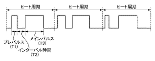
図22はダブルパルスの構成を示す図である。 FIG. 22 is a diagram showing the configuration of a double pulse.
図22に示すように、ダブルパルスでは、メインパルスの吐出タイミングの前に記録ヘッドに対する予熱信号(プレパルス)を発生させ、さらに、メインパルスとプレパルスとの間にインターバル時間を発生させる。これらのパルスの各時間において、記録ヘッドの温度補正、温度センサの感度のばらつきによる補正、ノズル毎の温度−吐出特性のばらつきによる補正等を反映させる。なお、メインパルスのパルス幅とインターバル時間とプレパルスのパルス幅はそれぞれ、T1、T2、T3とし、以下の説明でも同じ参照符号を用いる。 As shown in FIG. 22, in the double pulse, a preheating signal (prepulse) for the recording head is generated before the ejection timing of the main pulse, and an interval time is generated between the main pulse and the prepulse. At each time of these pulses, the correction of the temperature of the recording head, the correction due to the variation in the sensitivity of the temperature sensor, the correction due to the variation in the temperature-discharge characteristic for each nozzle, and the like are reflected. The pulse width of the main pulse, the interval time, and the pulse width of the pre-pulse are T1, T2, and T3, respectively, and the same reference numerals are used in the following description.
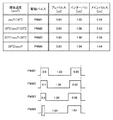
例えば、特許文献3では、環境温度に対してダブルパルスの各時間を調節する構成が開示されている。
For example,
図23は、特許文献3に開示する構成に基づいた、環境温度に対してダブルパルスの各時間を調節する例を示す図である。
FIG. 23 is a diagram illustrating an example of adjusting each time of the double pulse with respect to the environmental temperature based on the configuration disclosed in
図23によれば、例えば、環境温度(envT)が28度以上のときに駆動パルスとしてはPWM4が選択される。この場合、他の3つのパルス(PWM1〜PWM3)に比べて、パルスのスタート時間が遅れるが、原則としてダブルパルスのトータル時間は一定である。特に、メインパルスの立下りは吐出タイミングを揃えるために一定となっている。 According to FIG. 23, for example, when the environmental temperature (envT) is 28 degrees or higher, PWM4 is selected as the drive pulse. In this case, the start time of the pulse is delayed as compared with the other three pulses (PWM1 to PWM3), but in principle, the total time of the double pulse is constant. In particular, the fall of the main pulse is constant in order to align the discharge timing.
以上説明したような従来例の構成をとると、HE信号のパルス幅を任意に設定可能である。しかしながら、同一のヒート周期で複数回ヒータを駆動する場合、即ち、図22に示すようにHE信号パルスを複数回、与える場合には、複数のパルス時間分の基準電圧設定データが必要となるためデータ数が増加してしまう。その結果、記録装置の本体部から記録ヘッドへのデータ転送速度を上げたり、データを分割する等の対策が必要となる。これは、記録動作の信頼性の低下や、記録ヘッドの素子基板における端子数の増加という問題を生じさせる。また、複数のパルス幅データを設定しておくメモリも複数必要になるため回路規模も増大してしまう。 If the configuration of the conventional example as described above is taken, the pulse width of the HE signal can be arbitrarily set. However, when the heater is driven a plurality of times in the same heat cycle, that is, when the HE signal pulse is applied a plurality of times as shown in FIG. 22, reference voltage setting data for a plurality of pulse times is required. The number of data increases. As a result, measures such as increasing the data transfer speed from the main body of the recording apparatus to the recording head and dividing the data are required. This causes problems such as a decrease in the reliability of the recording operation and an increase in the number of terminals on the element substrate of the recording head. In addition, since a plurality of memories for setting a plurality of pulse width data are required, the circuit scale increases.
本発明は上記従来例に鑑みてなされたもので、より信頼性の高い記録動作を実現するとともに、素子基板のサイズの削減や、構成の簡素化を図った素子基板とこれを用いた記録ヘッドとその記録ヘッドを搭載した記録装置を提供することを目的とする。 The present invention has been made in view of the above-described conventional example, and realizes a more reliable recording operation, an element substrate in which the size of the element substrate is reduced, and the configuration is simplified, and a recording head using the same And a recording apparatus equipped with the recording head.
上記目的を達成するために本発明の素子基板は次のような構成からなる。 In order to achieve the above object, the element substrate of the present invention has the following configuration.
即ち、複数の記録素子と、前記複数の記録素子に対応して備えられ前記複数の記録素子を駆動する複数の駆動素子と、1つの基準電圧と傾きが異なる2つのランプ波とを入力してダブルパルスを生成し、前記ダブルパルスを前記複数の駆動素子に印加して前記複数の駆動素子を駆動する駆動回路とを有し、前記駆動回路は、前記1つの基準電圧と前記傾きが異なる2つのランプ波それぞれとを生成する生成回路と、前記1つの基準電圧と前記傾きが異なる2つのランプ波それぞれとを比較する比較回路とを有し、前記比較回路における比較の結果からパルス幅の異なるダブルパルスを生成することを特徴とする。 That is, a plurality of recording elements, a plurality of driving elements provided corresponding to the plurality of recording elements and driving the plurality of recording elements, and two ramp waves having different slopes from one reference voltage are input. A driving circuit that generates a double pulse and drives the plurality of driving elements by applying the double pulse to the plurality of driving elements, and the driving circuit has a slope different from that of the one reference voltage. A generation circuit that generates each of the two ramp waves, and a comparison circuit that compares the one reference voltage and each of the two ramp waves having different slopes, and the pulse widths differ from the result of the comparison in the comparison circuit. A double pulse is generated.
また本発明を別の側面から見れば、上記構成の素子基板を用いた記録ヘッド、特にインクジェット方式に従ってインクを吐出して記録を行うフルラインのインクジェット記録ヘッドを備える。 According to another aspect of the present invention, there is provided a recording head using the element substrate having the above-described configuration, particularly a full-line inkjet recording head that performs recording by discharging ink according to an inkjet method.
さらに本発明を別の側面から見れば、上記のフルライン記録ヘッドを用いて記録を行う記録装置を備える。 Further, from another aspect, the present invention includes a recording apparatus that performs recording using the above-described full line recording head.
従って本発明によれば、1つの基準電圧から複数のダブルパルスを生成することができるという効果がある。これにより、複数のダブルパルスの生成のために多くのデータを用いる必要もないので、多くのデータの転送や制御に必要であった構成をなくすことができる。これは素子基板のサイズの削減や簡素化、記録動作の高信頼性に資するものとなる。 Therefore, according to the present invention, there is an effect that a plurality of double pulses can be generated from one reference voltage. Thereby, since it is not necessary to use a lot of data for generating a plurality of double pulses, it is possible to eliminate the configuration necessary for transferring and controlling a lot of data. This contributes to reduction and simplification of the element substrate size and high reliability of the recording operation.
以下添付図面を参照して本発明の好適な実施例について、さらに具体的かつ詳細に説明する。なお、既に説明した部分には同一符号を付し重複説明を省略する。 Hereinafter, preferred embodiments of the present invention will be described more specifically and in detail with reference to the accompanying drawings. In addition, the same code | symbol is attached | subjected to the already demonstrated part and duplication description is abbreviate | omitted.
なお、この明細書において、「記録」(「プリント」という場合もある)とは、文字、図形等有意の情報を形成する場合のみならず、有意無意を問わない。また人間が視覚で知覚し得るように顕在化したものであるか否かを問わず、広く記録媒体上に画像、模様、パターン等を形成する、または媒体の加工を行う場合も表すものとする。 In this specification, “recording” (sometimes referred to as “printing”) is not limited to the case of forming significant information such as characters and graphics, but may be significant. It also represents the case where an image, a pattern, a pattern, etc. are widely formed on a recording medium, or the medium is processed, regardless of whether it is manifested so that humans can perceive it visually. .
また、「記録媒体」とは、一般的な記録装置で用いられる紙のみならず、広く、布、プラスチック・フィルム、金属板、ガラス、セラミックス、木材、皮革等、インクを受容可能なものも表すものとする。 “Recording medium” refers not only to paper used in general recording apparatuses but also widely to cloth, plastic film, metal plate, glass, ceramics, wood, leather, and the like that can accept ink. Shall.
さらに、「インク」(「液体」と言う場合もある)とは、上記「記録(プリント)」の定義と同様広く解釈されるべきものである。従って、記録媒体上に付与されることによって、画像、模様、パターン等の形成または記録媒体の加工、或いはインクの処理(例えば記録媒体に付与されるインク中の色剤の凝固または不溶化)に供され得る液体を表すものとする。 Further, “ink” (sometimes referred to as “liquid”) should be interpreted widely as in the definition of “recording (printing)”. Therefore, by being applied on the recording medium, it is used for formation of images, patterns, patterns, etc., processing of the recording medium, or ink processing (for example, solidification or insolubilization of colorant in the ink applied to the recording medium). It shall represent a liquid that can be made.
またさらに、「ノズル」とは、特にことわらない限り吐出口ないしこれに連通する液路およびインク吐出に利用されるエネルギーを発生する素子を総括して言うものとする。 Furthermore, unless otherwise specified, the “nozzle” collectively refers to an ejection port or a liquid channel communicating with the ejection port and an element that generates energy used for ink ejection.
以下に用いる記録ヘッド用の素子基板(ヘッド基板)とは、シリコン半導体からなる単なる基体を指し示すものではなく、各素子や配線等が設けられた構成を差し示すものである。 An element substrate (head substrate) for a recording head to be used below does not indicate a simple substrate made of a silicon semiconductor but indicates a configuration in which each element, wiring, and the like are provided.
さらに、基板上とは、単に素子基板の上を指し示すだけでなく、素子基板の表面、表面近傍の素子基板内部側をも示すものである。また、本発明でいう「作り込み(built-in)」とは、別体の各素子を単に基体表面上に別体として配置することを指し示している言葉ではなく、各素子を半導体回路の製造工程等によって素子板上に一体的に形成、製造することを示すものである。 Further, the term “on the substrate” means not only the element substrate but also the surface of the element substrate and the inside of the element substrate near the surface. In addition, the term “built-in” as used in the present invention is not a term indicating that each individual element is simply arranged separately on the surface of the substrate, but each element is manufactured in a semiconductor circuit. It shows that it is integrally formed and manufactured on an element plate by a process or the like.
次に、インクジェット記録装置の実施例について説明する。この記録装置は、ロール状に巻かれた連続シート(記録媒体)を使用し、片面記録及び両面記録の両方に対応した高速ラインプリンタであり。例えば、プリントラボ等における大量枚数のプリント分野に適している。 Next, examples of the ink jet recording apparatus will be described. This recording apparatus uses a continuous sheet (recording medium) wound in a roll shape, and is a high-speed line printer that supports both single-sided recording and double-sided recording. For example, it is suitable for a large number of print fields in a print laboratory or the like.
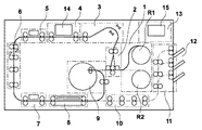
図1は本発明の代表的な実施例であるインクジェット記録装置(以下、記録装置)の内部概略構成を示す側断面図である。装置内部は大きくは、シート供給部1、デカール部2、斜行矯正部3、記録部4、クリーニング部(不図示)、検査部5、カッタ部6、情報記録部7、乾燥部8、シート巻取部9、排出搬送部10、ソータ部11、排出トレイ12、制御部13などに分けられる。シートは、図中の実線で示したシート搬送経路に沿ってローラ対やベルトからなる搬送機構で搬送され、各ユニットで処理がなされる。
FIG. 1 is a side sectional view showing a schematic internal configuration of an ink jet recording apparatus (hereinafter referred to as a recording apparatus) which is a typical embodiment of the present invention. The inside of the apparatus is roughly divided into a
シート供給部1はロール状に巻かれた連続シートを収納して供給するユニットである。シート供給部1は、2つのロールR1、R2を収納することが可能であり、択一的にシートを引き出して供給する構成となっている。なお、収納可能なロールは2つであることに限定はされず、1つ、あるいは3つ以上を収納するものであってもよい。デカール部2は、シート供給部1から供給されたシートのカール(反り)を軽減させるユニットである。デカール部2では、1つの駆動ローラに対して2つのピンチローラを用いて、カールの逆向きの反りを与えるようにシートを湾曲させてしごくことでカールを軽減させる。斜行矯正部3は、デカール部2を通過したシートの斜行(本来の進行方向に対する傾き)を矯正するユニットである。基準となる側のシート端部をガイド部材に押し付けることにより、シートの斜行が矯正される。
The
記録部4は、搬送されるシートに対して記録ヘッド部14によりシートの上に画像を形成するユニットである。記録部4は、シートを搬送する複数の搬送ローラも備えている。記録ヘッド部14は、使用が想定されるシートの最大幅をカバーする範囲でインクジェット方式のノズル列が形成されたフルライン記録ヘッド(インクジェット記録ヘッド)を有する。記録ヘッド部14は、複数の記録ヘッドがシートの搬送方向に沿って平行に配置されている。この実施例ではK(ブラック)、C(シアン)、M(マゼンタ)、Y(イエロ)の4色に対応した4つの記録ヘッドを有する。記録ヘッドの並び順はシート搬送上流側から、K、C、M、Yとなっている。なお、インク色数及び記録ヘッドの数は4つには限定はされない。また、インクジェット方式としては、発熱素子を用いた方式、ピエゾ素子を用いた方式、静電素子を用いた方式、MEMS素子を用いた方式等を採用することができる。各色のインクは、インクタンクからそれぞれインクチューブを介して記録ヘッド部14に供給される。
The
検査部5は、記録部4でシートに記録された検査パターンや画像を光学的に読み取って、記録ヘッドのノズルの状態、シート搬送状態、画像位置等を検査するユニットである。検査部5は実際に画像を読み取り画像データを生成するスキャナ部と読み取った画像を解析して記録部4へ解析結果を返す画像解析部より構成されている。検査部5はCCDラインセンサであり、シート搬送方向と垂直な方向にセンサが並べられている。
The
なお、上述のように図1に示した記録装置は、片面記録及び両面記録の両方に対応しているが、図2と図3とはそれぞれ、図1に示す記録装置において片面記録時の動作と両面記録時の動作を説明するための図である。 As described above, the recording apparatus shown in FIG. 1 is compatible with both single-sided recording and double-sided recording. FIGS. 2 and 3 are respectively the operations during single-sided recording in the recording apparatus shown in FIG. FIG. 6 is a diagram for explaining an operation during double-sided recording.
図4は記録ヘッド部14に搭載されるフルライン記録ヘッド100と記録媒体800の搬送方向の関係を示した図である。
FIG. 4 is a diagram showing the relationship between the full-
記録動作を行う際には、フルライン記録ヘッド100は記録装置に固定されており、記録媒体800が搬送され、素子基板101に設けられた複数の吐出口706からインクが吐出され、記録媒体800に画像が形成される。
When performing the recording operation, the full-
この図から分かるように、この例では、フルライン記録ヘッド100は4つの素子基板101を実装して構成されている。
As can be seen from this figure, in this example, the full
図5はフルライン記録ヘッドの分解斜視図である。 FIG. 5 is an exploded perspective view of the full-line recording head.
フルライン記録ヘッド100は4つの素子基板101−1、101−2、101−3、101−4、支持部材501、プリント配線板110、インク供給部材502等を備えている。図5に示すように、フルライン記録ヘッド100には4つの素子基板が千鳥状に配置されている。なお、搭載する素子基板101の数を増やすことでさらに記録幅の長い記録ヘッドを構成することが可能である。また、4つの素子基板を個別的に特定せずに説明する場合には、単に素子基板101として言及する。
The full
図5から分かるように、プリント配線板110は基本的には矩形形状、素子基板101は矩形形状をしている。そして、素子基板101の長手方向に複数の吐出口706が配列される。また、素子基板101の長手方向。つまり、複数の吐出口の配列方向がプリント配線板110の長手方向となるように配置される。
As can be seen from FIG. 5, the printed
次に、上記構成の記録装置に搭載するフルライン記録ヘッドに実装される素子基板に関しいくつかの実施例を説明する。 Next, some examples will be described with respect to the element substrate mounted on the full line recording head mounted on the recording apparatus having the above configuration.
この実施例を説明する前提として、次のようなHE信号を考慮する。 As a premise for explaining this embodiment, the following HE signal is considered.
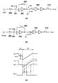
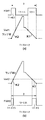
図20はランプ波と基準電圧(Ref)を比較することで、インクジェット記録ヘッド(以下、記録ヘッド)ではヒータを駆動する期間を決める信号であるヒートイネーブル(HE)信号パルスの変調に適用する。 FIG. 20 is applied to modulation of a heat enable (HE) signal pulse which is a signal for determining a period for driving a heater in an ink jet recording head (hereinafter, recording head) by comparing a ramp wave and a reference voltage (Ref).
図20において、200は時間に比例して(時間の経過とともに)電圧が上昇する波形をもつランプ波、Ref1〜Ref3は任意に設定可能な基準電圧(Ref)である。ランプ波200と基準電圧(Ref1〜Ref3)を比較し、両方の電圧が等しくなったところでパルスが立ち下がるようにしておくと設定した基準電圧によってパルス幅を変えることができる。例えば、基準電圧(Ref1)を設定したときはHE信号のパルス幅はHE1となり、基準電圧(Ref2)のときはHE2、基準電圧(Ref3)のときはHE3のパルス幅となる。このようにランプ波と基準電圧とを比較することによってパルス幅を任意に設定することができる。
In FIG. 20, 200 is a ramp wave having a waveform in which the voltage rises in proportion to time (with time), and Ref1 to Ref3 are reference voltages (Ref) that can be arbitrarily set. If the
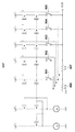
図21は基準電圧とランプ波とを比較するコンパレータの構成を示す図である。 FIG. 21 is a diagram illustrating a configuration of a comparator that compares the reference voltage and the ramp wave.
このコンパレータは、コンデンサから成るメモリ部201と、スイッチ203とインバータ204から成る比較部202と、波形を出力するためのバッファ205とから構成される。このコンパレータは、メモリ部201に基準電圧(Ref)を記憶し、その後、入力されたランプ波と比較する。なお、このコンパレータの入力部と出力部とにはそれぞれスイッチ209、210が設けられる。
The comparator includes a
即ち、図22に示すような、一ヒート周期にプレパルス、インターバル時間、メインパルスを含むダブルパルスのHE信号を用いる。また、図23に示した特許文献3に開示されているPWM1〜4のように、プレパルス(T1)とインターバル時間(T2)とメインパルス(T3)とからなるダブルパルスのトータル時間は固定(即ち、T1+T2+T3は一定)であるとする。また、例えば、PWM4ではPWM1〜3と比べて、プレパルスの立ち上がりが少し遅れるが、吐出タイミングを揃えるためにメインパルスの立下りは固定である。
That is, as shown in FIG. 22, a double pulse HE signal including a pre-pulse, an interval time, and a main pulse is used in one heat cycle. 23, the total time of the double pulse composed of the pre-pulse (T1), the interval time (T2), and the main pulse (T3) is fixed (ie, PWM 1-4 disclosed in
次に、以上のような構成を前提として、ダブルパルスのHE信号を1つの基準電圧で生成する方法を説明する。また、ここでは、素子基板内のばらつき(例えば、温度分布やヒータ抵抗ばらつき、保護膜の膜厚分布等)に応じてヒータ(記録素子)毎にHE信号のパルス幅を制御してダブルパルスを生成する方法について述べる。実際は、DACを用いて階段波を生成するが、ここでは説明を簡単にするために一定の傾きをもつランプ波を用いる。 Next, on the premise of the above configuration, a method of generating a double pulse HE signal with one reference voltage will be described. Also, here, a double pulse is generated by controlling the pulse width of the HE signal for each heater (recording element) according to variations in the element substrate (for example, temperature distribution, heater resistance variation, protective film thickness distribution, etc.). A generation method will be described. Actually, a staircase wave is generated using a DAC, but a ramp wave having a certain slope is used here for the sake of simplicity.
図6は、この実施例に従ってダブルパルスのヒートイネーブル(HE)信号を生成する様子を示すタイムチャートである。 FIG. 6 is a time chart showing how a double-pulse heat enable (HE) signal is generated according to this embodiment.
まず、図6(a)はプレパルス幅(T1)とメインパルス幅(T3)の比を1:4に設定する場合を示す。基準電圧がVref1の場合、メインパルスのランプ波の傾きK1を基準とすると、プレパルス幅を作る場合は4倍の傾きK2のランプ波を入力する。パルスの時間の絶対値は、基準電圧Vref1で決定する。時間傾きK2のランプ波が基準電圧を超えてから、傾きK2のランプ波の立下りのタイミングまでの時間がインターバル時間(T2)である。この実施例では、傾きK2のランプ波の立下りのタイミングを、メインパルスの開始タイミングに一致させている。メインパルスランプ波が終わり、次のランプ波が入力されるまでコンパレータのスイッチ209をOFFしておけばよい。なお、コンパレータは比較回路とも呼ばれる。
First, FIG. 6A shows a case where the ratio of the pre-pulse width (T1) to the main pulse width (T3) is set to 1: 4. When the reference voltage is Vref1, when the ramp pulse K1 of the main pulse is used as a reference, a ramp wave having a quadruple gradient K2 is input to create a prepulse width. The absolute value of the pulse time is determined by the reference voltage Vref1. The time from when the ramp wave with the time gradient K2 exceeds the reference voltage to the falling timing of the ramp wave with the gradient K2 is the interval time (T2). In this embodiment, the fall timing of the ramp wave having the slope K2 is made coincident with the start timing of the main pulse. The
次に、プレパルス幅(T1)とメインパルス幅(T3)の比を1:3に設定する場合を図6(b)に示す。基準電圧をVref1、プレパルスのランプ波の傾きをK2のまま、メインパルスのランプ波の傾きをK1aとする。この傾きK1aは傾きK2の3分の1である。これにより、プレパルス幅(T1)とインターバル時間(T2)を一定にしたまま、メインパルスのパルス幅を短くすることができる。 Next, FIG. 6B shows a case where the ratio of the pre-pulse width (T1) to the main pulse width (T3) is set to 1: 3. The reference voltage is Vref1, the slope of the prepulse ramp wave is K2, and the slope of the main pulse ramp wave is K1a. This inclination K1a is one third of the inclination K2. Thereby, the pulse width of the main pulse can be shortened while keeping the pre-pulse width (T1) and the interval time (T2) constant.
次に、プレパルス幅(T1)とメインパルス幅(T3)の比は1:4のままプレパルス幅(T1)とメインパルス幅(T3)の絶対値を大きくする場合を図6(c)に示す。この場合には、基準電圧をVref1より高い電圧であるVref2に設定する。メインパルスのランプ波の傾きはK1、プレパルス幅のランプ波の傾きはK2とする。 Next, FIG. 6C shows a case where the absolute value of the prepulse width (T1) and the main pulse width (T3) is increased while the ratio between the prepulse width (T1) and the main pulse width (T3) is 1: 4. . In this case, the reference voltage is set to Vref2, which is a voltage higher than Vref1. The slope of the ramp wave of the main pulse is K1, and the slope of the ramp wave of the prepulse width is K2.
このように、設定した1つの基準電圧(Vref)に対してランプ波の傾きを変えること、ランプ波の傾きを変えずに基準電圧(Vref)を変えることで任意のダブルパルスを生成することができる。なお、補足すると、プレパルスのランプ波は、後述する基準電圧の入力に続いて行われる。 Thus, an arbitrary double pulse can be generated by changing the slope of the ramp wave with respect to one set reference voltage (Vref) or changing the reference voltage (Vref) without changing the slope of the ramp wave. it can. In addition, supplementally, the prepulse ramp wave is performed subsequent to the input of a reference voltage described later.
ここで、ヒータ毎に個別にパルス幅を調整する方法について説明する。 Here, a method for individually adjusting the pulse width for each heater will be described.
図7は記録ヘッドの素子基板のレイアウトを模式的に示す図である。 FIG. 7 is a diagram schematically showing the layout of the element substrate of the recording head.
図7に示す例では、素子基板101には2つのインク供給口601が形成され、各インク供給口に対応した回路ブロックには、そのインク供給口を挟んで対向する位置にヒータ602を列状に配置している。さらに、このヒータ列のヒータを選択駆動する駆動回路605がヒータ602に対応して配置されている。また、これらのヒータや駆動回路への電源供給や信号印加を行うパッド604が素子基板101の上下端部に配置されている。
In the example shown in FIG. 7, two
また、素子基板101の上辺に沿ったパッド604とインク供給口601、ヒータ列との間には、駆動回路603が配置される。さらに、ヒータ602の背後に設けられた駆動回路605の近傍にはコンパレータ609が配置される。
A
一方、素子基板101の下辺に沿ったパッドと、インク供給口601、ヒータ列との間には、OPアンプ606、DAC(デジタル/アナログ変換器)607が配置される。このような回路レイアウト構成をとることで、ヒータ毎に個別にHE信号のパルス幅を設定できるようになり、ヒータ毎に適正なエネルギーを与えることが可能である。
On the other hand, an
図8は図7に示す回路レイアウトの一部の回路構成の詳細と信号の流れを模式的に示す図である。 FIG. 8 is a diagram schematically showing the details of a part of the circuit configuration of the circuit layout shown in FIG. 7 and the signal flow.
パッド604に印加されるデータ信号(DATA_A_1)はクロック信号(CLK)、ラッチ信号(LT)、記録データ信号(DATA)などを含んでおり、入力回路702を介して内部回路を構成するシフトレジスタ703やデコーダ704へと入力される。ここで、記録データ信号(DATA)はあるヒート期間で駆動するヒータを選択する信号である。
A data signal (DATA_A_1) applied to the
また、データ信号として、各回路ブロックによって異なるパッドより別の信号が入力される。入力されたデータ信号はシフトレジスタ703で展開され、その一部は記録データ信号(DATA)として複数配置されたヒータ駆動グループ707へと入力され、ヒータ駆動グループの有効・無効を選択する。また、展開されたデータ信号の別の一部は、デコーダ704へと入力される。デコーダ704は、ヒータ駆動グループ内で駆動するヒータを順次切替える時分割信号(BLKn)706を出力する。ここで、1グループ内に含まれるヒータの個数を2n個とすると、2n個の時分割信号が必要となる。
As a data signal, another signal is input from a different pad depending on each circuit block. The input data signal is developed by the
ここで、1つのヒータ駆動グループにはヒータ列の中で近接して連続して素子基板上に設けられる2n個のヒータが含まれる。この2n個が時分割駆動される。そして、このグループ単位にコンパレータ(比較回路)が1つずつ備えられる。 Here, one heater drive group includes 2 n heaters provided on the element substrate in close proximity to each other in the heater array. These 2 n are time-division driven. One comparator (comparison circuit) is provided for each group.
さらに、データ信号のさらに別の一部であるHEデータ(HENB)がDAC用シフトレジスタ708、DAC607、OPアンプ606を経て、コンパレータ(COMP)711へと供給される。そして、コンパレータ609でヒートイネーブル(HEn)信号が生成される。図8の例では8つのHE信号(HE1〜8)が生成される。
Further, HE data (HENB), which is still another part of the data signal, is supplied to the comparator (COMP) 711 via the
DAC607はディジタルデータで設定したアナログ電圧値を生成できる回路(生成回路)である。この実施例では任意の電圧値を生成できることを利用して、DAC607を基準電圧(Ref)とランプ波の生成に用いている。シフトレジスタ708はデータ信号に含まれるHEパルス幅を決めるHEデータ(HENB)をシフトレジスタ703から受信し、DAC607へ転送する。DAC607にはOPアンプ606を介して複数グループのコンパレータ(Comp)609が接続される。
The
コンパレータ(Comp)609はDAC607の負荷として作用するため、直接接続すると応答速度が遅くなり出力波形が鈍ってしまう。一方、OPアンプ606は負帰還をかけると入力と出力を等しくしようと動作する。これを利用してDAC607とコンパレータ609との間にOPアンプ606を挿入する。これにより、DAC607の負荷はOPアンプ606だけとなり、DAC607の出力と同様な波形をコンパレータ609へ出力することができる。この様にして、基準電圧とランプ波をDAC607で生成し、コンパレータ609へ転送する。
Since the comparator (Comp) 609 acts as a load of the
図9はコンパレータ609の動作を説明する図である。
FIG. 9 is a diagram for explaining the operation of the
図9に示すコンパレータ609の回路構成は、図21で説明したものと同じなので、ここでは同じ参照番号を付して、その説明は省略する。図9(a)はスイッチ203が閉じている状態を示し、図9(b)はスイッチ203が開いている状態を示す。次に、コンパレータ609の動作を図9(c)を参照して説明する。図9(c)にはコンパレータ609の入力電圧Vin、インバータ204の入力電圧Va、コンパレータ609の出力電圧Voutの電圧の時間変化が示されている。
Since the circuit configuration of the
まず、期間t1において、スイッチ203とスイッチ209を閉じる。スイッチ203を閉じることによって、インバータ204の入力と出力が短絡され、コンデンサ201のインバータ204側の電極の電位VaがVthとなる。Vthは、インバータ204の閾値電圧である。スイッチ209を閉じることで、コンデンサ201のスイッチ209側の電極の電位がVrefとなる。これにより、コンデンサ201にはVth−Vrefに相当する電荷が充電される(別の表現をするとコンデンサ201にはVth−Vrefの電位差がかかる)。
First, in a period t1, the
次に、期間t2において、スイッチ203を開く。メモリ部201のコンデンサの両端にはVth−Vrefの電位差が維持される。スイッチ209を閉じて(図9(b))、Vinとしてランプ波Vramp(図9(c)を入力する。ランプ波Vrampの入力によって、Va=Vref−Vth+Vrampとなる。ここで、入力されるランプ波Vrampの電位は、当初Vrefの電位より低く設定されているので、Vaはインバータ204の閾値電圧Vthより低くなる。このため、インバータ204はHレベルを出力する。これにより、Voutが立ち上がる。ランプ波Vrampの電位は、時間の経過とともに徐々に高くなっていくが、ランプ波Vrampの電位はVrefの電位より低い間は、インバータ204はHレベルを出力する。そして、ランプ波Vrampの電位がVrefの電位を超えたとき、Vaの電位がVthより高くなり、インバータ204はLレベルを出力する。これにより、Voutが立ち下がる。以上のようにして、図9(c)に示すように、Voutからパルスが出力される。
Next, in the period t2, the
以上のように、コンパレータでは、メモリ部にチャージした基準電圧Vrefとランプ波でパルス幅を調整する。このように、この実施例のコンパレータはメモリ部にコンデンサを備え、比較部にインバータを備える構成であるので、回路規模が小さく基板面積を抑制するために有利である。 As described above, the comparator adjusts the pulse width with the reference voltage Vref charged in the memory portion and the ramp wave. As described above, the comparator of this embodiment is configured to include the capacitor in the memory unit and the inverter in the comparison unit, which is advantageous in that the circuit scale is small and the board area is suppressed.
次に、DAC607について説明する。
Next, the
図10はランプ波と基準電圧(Vref)を生成するDAC607の構成を示す回路図である。図10は4ビットDACの構成例を示しており、901〜905は各ビットをON/OFFするスイッチで、906、907は電圧に変換する抵抗である。
FIG. 10 is a circuit diagram showing a configuration of a
DAC607は複数のカレントミラー回路を並列に接続した構成を用い、各カレントミラー回路の出力部に設けられたスイッチ901〜905を制御し、抵抗に流れる電流を調整することで任意の電圧を生成する。この構成では、スイッチ902〜905からの出力が4ビットの各ビットに対応している。
The
さて、スイッチ902をONすると電流Iが流れるため出力端子OUTからは、(R/2+R/2)×I=RIの電圧が出力される。さらに、スイッチ903をONすると2×RI、スイッチ904をONすると3×RI、スイッチ905をONすると4×RIが出力される。このようにスイッチをON/OFFすることで任意の電圧を生成することができる。
When the
さて、この実施例では、基準電圧(Vref)とランプ波を共通のDACで生成するので、1つのDACでランプ波と半階調ずらした基準電圧(Vref)を生成できるようにしたい。このような理由から、DAC607は、抵抗Rを抵抗906と907のようにR/2ずつにわけ、その間にスイッチ901で制御される電流が流れるような構成となっている。従って、DACを共通化しない場合はこのような構成を取る必要はない。また、MOSのサイズ比で電流の重みづけをする等、他の構成を取ることもできる。
In this embodiment, since the reference voltage (Vref) and the ramp wave are generated by a common DAC, it is desired to generate a reference voltage (Vref) that is shifted from the ramp wave by a half tone with a single DAC. For this reason, the
図11はヒータ駆動グループ707の内部構成を示す回路図である。
FIG. 11 is a circuit diagram showing the internal configuration of the
なお、図8から分かるように、図11に示すのと同様のヒータ駆動グループが複数、素子基板101には実装される。
As can be seen from FIG. 8, a plurality of heater drive groups similar to those shown in FIG. 11 are mounted on the
ヒータ駆動グループ707は、アレイ状に配置されたヒータ602に対応して配置される、駆動素子1004、電圧変換回路(LVC)1005、ヒータ選択回路1006からなる。ヒータ電源配線1001は外部から供給されるヒータ電源電圧(VH:第1電源電圧)が印加されており、ヒータ602を通ってグランド(GNDH)1002へ電流が流れる。
The
ここで、駆動素子1004はヒータ602に通電するかどうかの決めるスイッチ素子としての機能を果たす。記録データ信号線1007、時分割信号1008、ヒートイネーブル信号線1009からの信号はヒータ選択回路1006であるANDゲートへと入力され、これら3つの信号が共にアクティブとなった場合にそのANDゲートの出力がアクティブとなる。このANDゲートの出力信号は、電圧変換回路1005によりその信号の電圧振幅を、入力回路702からヒータ選択回路1006までの駆動電圧(VDD第3電源電圧)よりも高い電源電圧(VHM:第2電源電圧)にレベル変換(昇圧)される。レベル変換された信号は、駆動素子1004のゲートに印加され、ゲート電圧が印加されたMOSトランジスタに接続されたヒータ602は通電、駆動されることとなる。
Here, the
このようなヒータ毎に個別制御する構成で、図6に示した基準電圧(Vref)とランプ波を入力し、ダブルパルスを生成する。 In such a configuration in which each heater is individually controlled, the reference voltage (Vref) and the ramp wave shown in FIG. 6 are input to generate a double pulse.
まず、図8に示す例では、8つのヒータ駆動グループ707の基準電圧(Vref)をDAC607で生成し、スイッチを切り換えながらコンパレータ609のメモリに順次記憶していく。全てのグループのコンパレータに基準電圧(Vref)を記憶させた後、全グループ同時にランプ波を入力する。同時入力することで同じタイミングでコンパレータ609によってランプ波と基準電圧(Vref)とが比較され、各グループに設定された基準電圧(Vref)に応じたHE信号パルスが生成される。
First, in the example shown in FIG. 8, the reference voltage (Vref) of the eight
この実施例ではダブルパルスを生成するので、図6に示すように2回のランプ波が入力される度にダブルパルスが生成される。 In this embodiment, since a double pulse is generated, a double pulse is generated every time two ramp waves are input as shown in FIG.
次に、ランプ波の傾きを変化させる3種類の方法について説明する。 Next, three methods for changing the slope of the ramp wave will be described.
(1)第1の方法(DACの抵抗を切り替える方法)
図12は抵抗を切り替える構成を備えたDAC607の回路図である。
(1) First method (method of switching DAC resistance)
FIG. 12 is a circuit diagram of the
電流をカレントミラー回路により生成する構成は図10と同じであるので、図12においても、図10で説明したのと同じ構成要素には同じ参照番号を付し、その説明は省略する。この構成では、図10に示した抵抗906、907の抵抗値をスイッチ1116〜1125のON/OFFで選択できるようになっている。出力端子OUTには電流I×抵抗値の電圧が出力される。
Since the configuration for generating the current by the current mirror circuit is the same as in FIG. 10, the same reference numerals are given to the same components as those described in FIG. 10 in FIG. In this configuration, the resistance values of the
従って、この抵抗値を切り換えることによってランプ波の傾きを変えることができる。例えば、スイッチ1116と1117をONしたときスイッチ902〜905を順番にONしていくと3R×I、3R×2I、3R×3I、3R×4Iの電圧が順次出力されランプ波が生成される。次に、スイッチ1118と1119をONすると、2.1R×I、2.1R×2I、2.1R×3I、2.1R×4Iの電圧が順次出力されランプ波全体の電圧が圧縮される。クロック信号(CLK)に応じてスイッチ902〜905がONされるため昇圧する時間は変わらないので、ランプ波の傾きが変わることになる。このように抵抗を切り替えることによってランプ波の傾きを変えることが可能となり、図12に示した抵抗比とすることによって図23に示した駆動パルスPWM1〜4を生成することができる。
Therefore, the slope of the ramp wave can be changed by switching the resistance value. For example, when the
(2)第2の方法(DACのミラー比を切り替える方法)
図13はカレントミラー比を切り替える構成を備えたDAC607の回路図である。
(2) Second method (method of switching the mirror ratio of DAC)
FIG. 13 is a circuit diagram of the
電流をカレントミラー回路により生成する構成は図10と同じであるので、図13においても、図10で説明したのと同じ構成要素には同じ参照番号を付し、その説明は省略する。この構成では、電流源1209、1210の部分を1211、1212のようにカレントミラー構成とし、各MOSにサイズ比をつけスイッチ1213、1214で選択することでスイッチ902〜905に流れる電流値を変更可能にしている。
Since the configuration for generating the current by the current mirror circuit is the same as in FIG. 10, the same reference numerals are given to the same components as those described in FIG. 10 in FIG. 13, and the description thereof is omitted. In this configuration, the
出力端子OUTからはR×電流値の電圧が出力されるので、例えば、カレントミラー部1211、カレントミラー部1212のサイズ比3のMOSFETがONしている場合、3Iの電流がミラーされる。この場合、スイッチ902〜905にも3Iの電流が流れるので、出力端子OUTからはR×3I〜R×12Iの電圧が出力される。これと比較し、サイズ比2.1のMOSFETを選択した場合、出力端子OUTからはR×2.1I〜R×8.4Iの電圧が出力されランプ波全体の電圧が圧縮される。クロック信号(CLK)に応じてスイッチ902〜905がONされるため昇圧する時間は変わらないので、ランプ波の傾きが変わることになる。また、図13のようなサイズ比とすることによって図23に示した駆動パルスPWM1〜4を生成することができる。
Since a voltage of R × current value is output from the output terminal OUT, for example, when a MOSFET having a size ratio of 3 between the
(3)第3の方法(コンパレータの容量を切り替える方法)
図14は容量を切り替える構成を備えたコンパレータ609の回路図である。
(3) Third method (method of switching the capacitance of the comparator)
FIG. 14 is a circuit diagram of a
なお、コンパレータの基本的な構成は図21に示したコンパレータと同じであるので、図14においても、図21で説明したのと同じ構成要素には同じ参照番号を付し、その説明は省略する。この構成では、Vinに入力された基準電圧(Vref)をメモリ(第1のコンデンサ)201にスイッチ203がONしている状態で記憶する。その後、スイッチ203をOFFに切り換えてランプ波を入力するとVramp=基準電圧(Vref)となったところでインバータ204の出力が反転する。
Since the basic configuration of the comparator is the same as that of the comparator shown in FIG. 21, the same components as those described in FIG. 21 are denoted by the same reference numerals in FIG. . In this configuration, the reference voltage (Vref) input to Vin is stored in the memory (first capacitor) 201 with the
これに加え、この実施例では電圧可変用のメモリ1307、即ち、新たなコンデンサをメモリ部201として機能するコンデンサに直列となるように挿入する。また、説明のためにGND接地容量1309を挿入する。このようにすると、インバータ204の入力電圧Vaは、入力されたVinを電圧可変用メモリ1307とメモリ部201、GND接地容量1309で分圧した値となる。
In addition, in this embodiment, a
例えば、図14に示すようにメモリ部201とGND接地容量1309が1pFであり、図23に示す駆動パルスPWM1〜4を生成する場合、電圧可変用メモリ1307を1.17pF、0.59pF、0.35pF、0.11pFに順次切り替えればよい。Vin=1[V]とすると、電圧可変用メモリ1307が挿入されていないスイッチを選択すると、Va=0.5[V]となる。これに対して、電圧可変用メモリ1307の容量が1.17pFのコンセンサを選択すると、Va=0.35[V]となり電圧Vaが圧縮される。従って、Vinにランプ波が入力されるとVaでランプ波の傾きが変化する。
For example, as shown in FIG. 14, when the
このように、容量値が互いに異なるコンデンサ(第2のコンデンサ)を複数用いて電圧可変用メモリを構成し、スイッチ1308で選択することでランプ波の傾きを選択することができる。この容量を挿入する方法では直列にメモリ部201に直列に挿入するので合成容量が下がりランプ波の傾きが小さくなる。従って、この容量で調整する方法は傾きを小さくなる方向の調整となるため、ここでは、プレパルス幅(T1)を基準とし、メインパルスのランプ波の傾きを変更する場合を想定した容量比を説明した。
In this way, a voltage variable memory is configured using a plurality of capacitors (second capacitors) having different capacitance values, and the slope of the ramp wave can be selected by selecting with the
従って以上説明した実施例に従えば、1つの基準電圧(Vref)から複数のパルス幅をもつパルスを生成することができる。この結果、複数のパルスを生成するのに多くのデータを用いる必要がない。そのため、データ転送速度を上げたり、データを分割して転送する等の対策も不要となる。また、メモリを増やす必要もないため回路規模の増大も防ぐことができる。 Therefore, according to the embodiment described above, a pulse having a plurality of pulse widths can be generated from one reference voltage (Vref). As a result, it is not necessary to use a lot of data to generate a plurality of pulses. Therefore, measures such as increasing the data transfer speed or dividing and transferring data are not required. Further, since it is not necessary to increase the memory, an increase in circuit scale can be prevented.
ここでは実施例1で示したのとは異なるランプ波を用いてダブルパルスを生成する例について説明する。 Here, an example in which a double pulse is generated using a ramp wave different from that shown in the first embodiment will be described.
図15は、この実施例に従ってダブルパルスのヒートイネーブル(HE)信号を生成する様子を示すタイムチャートである。プレパルス用のランプ波は、時間の経過とともに電圧の値が一定の割合で高くなり、メインパルス用のランプ波は、時間の経過とともに電圧の値が一定の割合で低くなる。図15と図6とを比較すると分かるように、この実施例では、メインパルス用ランプ波の波形がプレパルス用のランプ波のそれに対して反転している。 FIG. 15 is a time chart showing how a double pulse heat enable (HE) signal is generated according to this embodiment. The pre-pulse ramp wave increases in voltage at a constant rate as time passes, and the main pulse ramp wave decreases in voltage value at a constant rate as time elapses. As can be seen by comparing FIG. 15 and FIG. 6, in this embodiment, the waveform of the main pulse ramp wave is inverted with respect to that of the pre-pulse ramp wave.
まず、図15(a)はプレパルス幅(T1)とメインパルス幅(T3)の比を1:2に設定する場合を示す。基準電圧がVref1の場合において、メインパルスのランプ波の傾きK1を基準とすると、プレパルス幅を作る場合は2倍の傾きK2のランプ波を入力する。パルスの時間の絶対値は、基準電圧Vref1で決定する。傾きK2のランプ波が基準電圧を超えてから、傾きK1のランプ波が基準電圧を下回るまでの時間が、インターバル時間(T2)である。補足すると、プレパルスのランプ波の開始からメインパルスのランプ波の終了までの時間が、プレパルスの開始からメインパルスの終了までの時間を決定する。 First, FIG. 15A shows a case where the ratio of the pre-pulse width (T1) to the main pulse width (T3) is set to 1: 2. When the reference voltage is Vref1 and the slope K1 of the ramp wave of the main pulse is used as a reference, a ramp wave having a double slope K2 is input to create a prepulse width. The absolute value of the pulse time is determined by the reference voltage Vref1. The time from when the ramp wave with the slope K2 exceeds the reference voltage until the ramp wave with the slope K1 falls below the reference voltage is the interval time (T2). Supplementally, the time from the start of the prepulse ramp wave to the end of the main pulse ramp wave determines the time from the start of the prepulse to the end of the main pulse.
次に、図15(b)はプレパルス幅(T1)とメインパルス幅(T3)の比を1:4に設定する場合を示す。基準電圧をVref1、プレパルスのランプ波の傾きをK2のまま、メインパルスのランプ波の傾きをK1aとする。この傾きK1aは傾きK2の4分の1である。これにより、プレパルスの開始からメインパルスの終了までの時間を一定にしたまま、メインパルスのパルス幅を長くすることができる。 FIG. 15B shows a case where the ratio of the pre-pulse width (T1) to the main pulse width (T3) is set to 1: 4. The reference voltage is Vref1, the slope of the prepulse ramp wave is K2, and the slope of the main pulse ramp wave is K1a. This inclination K1a is a quarter of the inclination K2. Thereby, the pulse width of the main pulse can be increased while keeping the time from the start of the pre-pulse to the end of the main pulse constant.
さらに、図15(c)はプレパルス幅(T1)とメインパルス幅(T3)の比は1:2のままプレパルス幅(T1)とメインパルス幅(T3)の絶対値を大きくする場合を示す。この場合には、基準電圧をVref1より高い電圧であるVref2に設定する。メインパルスのランプ波の傾きはK1、プレパルス幅のランプ波の傾きはK2とする。 Further, FIG. 15C shows a case where the absolute value of the prepulse width (T1) and the main pulse width (T3) is increased while the ratio of the prepulse width (T1) to the main pulse width (T3) is 1: 2. In this case, the reference voltage is set to Vref2, which is a voltage higher than Vref1. The slope of the ramp wave of the main pulse is K1, and the slope of the ramp wave of the prepulse width is K2.
このように、メインパルスを反転させると、その開始時間と終了時間をダブルパルスのトータル時間と合わせて固定することができるので、トータル時間が固定の場合、パルス幅に合わせてランプ波の傾きを変えるだけでよく制御が簡単になる。 In this way, when the main pulse is inverted, its start time and end time can be fixed together with the total time of the double pulse, so if the total time is fixed, the slope of the ramp wave is adjusted to the pulse width. It is easy to control just by changing.
しかし、プレパルス用ランプ波が終了して立ち下がるときと、メインパルス用ランプ波の開始時に立ち上がるときにその電圧が基準電圧(Vref)を横切るためコンパレータからパルスが出力してしまう。従って、このときコンパレータのスイッチ210をOFFしておく必要がある。なお、補足すると、実施例1と同様にプレパルスのランプ波は、図9で説明したように基準電圧の入力に続いて行われる。
However, when the pre-pulse ramp wave ends and falls, and when the main pulse ramp wave starts, the voltage crosses the reference voltage (Vref), so a pulse is output from the comparator. Therefore, it is necessary to turn off the
この実施例では実施例1、2で用いた波形パターン以外のランプ波を用いる例について説明する。
In this embodiment, an example in which a ramp wave other than the waveform pattern used in
図16はこの実施例に従ってダブルパルスのヒートイネーブル(HE)信号を生成する様子を示すタイムチャートである。 FIG. 16 is a time chart showing how a double-pulse heat enable (HE) signal is generated according to this embodiment.
この例は、プレパルス用ランプ波の波形に対してメインパルス用ランプ波の波形が反転し、プレパルス用ランプ波とメインパルス用ランプ波との間でランプ波を立ち下げない形のランプ波を用いる例である。図16(a)は基準電圧としてVref1を用いた例を示し、図16(b)はVref2を用いた例を示す。 In this example, the waveform of the main pulse ramp wave is inverted with respect to the waveform of the prepulse ramp wave, and a ramp wave that does not fall between the prepulse ramp wave and the main pulse ramp wave is used. It is an example. FIG. 16A shows an example using Vref1 as a reference voltage, and FIG. 16B shows an example using Vref2.
このランプ波は実施例2と同様にランプ波の開始時間と終了時間をダブルパルスのトータル時間と合わせて固定することができるので、基準電圧(Vref)を変更するだけでプレパルス幅、インターバル時間、メインパルス幅を変更することができる。 Since this ramp wave can fix the start time and end time of the ramp wave together with the total time of the double pulse in the same manner as in the second embodiment, the prepulse width, the interval time, only by changing the reference voltage (Vref), The main pulse width can be changed.
例えば、図16(a)に示した基準電圧(Vref1)を図16(b)に示した基準電圧(Vref2)に変更すると実施例2と同様にT1:T3の比は一定で、T1、T2、T3が基準電圧(Vref)に応じて変化する。これに加えて、この実施例に従うランプ波はプレパルス用ランプ波の終了後立ち下げないため基準電圧(Vref)を横切ることがない。従って、実施例2のようにコンパレータのスイッチをOFFする必要がなくなり制御がさらに簡単になる。また、プレパルス用ランプ波の終了からメインパルス用ランプ波の開始までにランプ波の傾きを切り替えるが、その切り替えタイミングは間に入っていればどこでもよく、図16ではダブルパルスの真ん中で切り替える例を示している。 For example, when the reference voltage (Vref1) shown in FIG. 16 (a) is changed to the reference voltage (Vref2) shown in FIG. 16 (b), the ratio of T1: T3 is constant as in the second embodiment, and T1, T2 , T3 changes according to the reference voltage (Vref). In addition, since the ramp wave according to this embodiment does not fall after the end of the pre-pulse ramp wave, it does not cross the reference voltage (Vref). Therefore, it is not necessary to turn off the comparator switch as in the second embodiment, and the control is further simplified. Further, the slope of the ramp wave is switched from the end of the pre-pulse ramp wave to the start of the main pulse ramp wave, but the switching timing can be anywhere, and in FIG. 16, an example of switching in the middle of a double pulse is shown. Show.
次に、図16に示したランプ波を用いて図23に示す駆動パルスPWM1〜4を生成する方法について説明する。 Next, a method for generating the drive pulses PWM1 to PWM4 shown in FIG. 23 using the ramp wave shown in FIG. 16 will be described.
図17はこの実施例に従った駆動パルスPWM1〜4の生成の様子を示す図である。 FIG. 17 is a diagram showing how the drive pulses PWM1 to PWM4 are generated according to this embodiment.
図17(a)はメインパルス幅を基準にして駆動パルスを生成する様子を示し、図17(b)はプレパルス幅を基準にして駆動パルスを生成する様子を示している。 FIG. 17A shows a state where the drive pulse is generated based on the main pulse width, and FIG. 17B shows a state where the drive pulse is generated based on the pre-pulse width.
図17(a)の例では、メインパルス幅(T3)を基準にして、メインパルス用ランプ波の傾きを基準に基準電圧Vref1〜Vref4を決める。次に、プレパルス用ランプ波の傾きを基準電圧(Vref)とPWM1〜4のプレパルス幅(T1)に応じて変化させると、ランプ波の電圧波形はramp1〜ramp4のようになる。 In the example of FIG. 17A, the reference voltages Vref1 to Vref4 are determined based on the slope of the main pulse ramp wave with reference to the main pulse width (T3). Next, when the slope of the prepulse ramp wave is changed according to the reference voltage (Vref) and the prepulse width (T1) of PWM1 to 4, the ramp wave voltage waveform becomes ramp1 to ramp4.
また、図17(b)に示すように、プレパルス幅(T1)を基準にメインパルスのランプ波の傾きを変化させることもできる。また、プレパルス用ランプ波、メインパルス用ランプ波両方の傾きを変化させてもよい。なお、補足すると、実施例1、実施例2と同様に、プレパルスのランプ波は、図9で説明したように基準電圧の入力に続いて行われる。 Further, as shown in FIG. 17B, the slope of the ramp wave of the main pulse can be changed based on the pre-pulse width (T1). The slopes of both the prepulse ramp wave and the main pulse ramp wave may be changed. Supplementally, as in the first and second embodiments, the prepulse ramp wave is performed following the input of the reference voltage as described with reference to FIG.
図18はプレパルスを基準としてメインパルス用ランプ波の傾きを変化させて異なる駆動パルスPWM1〜4を求める場合に3つの異なる方法を用いる際に必要な値をまとめた表を示す図である。 FIG. 18 is a diagram showing a table summarizing values required when three different methods are used when different drive pulses PWM1 to PWM4 are obtained by changing the slope of the main pulse ramp wave with reference to the prepulse.
図18では、(1)DACの抵抗比で変える方法、(2)DACのミラー比で変える方法、(3)コンパレータの容量比で変える方法のそれぞれの場合の比を示している。図18に示す比とすることで図23に示すPWM1〜4を生成することができる。 FIG. 18 shows ratios in each case of (1) a method of changing by the DAC resistance ratio, (2) a method of changing by the DAC mirror ratio, and (3) a method of changing by the capacitance ratio of the comparator. By setting the ratio shown in FIG. 18, PWM1 to PWM4 shown in FIG. 23 can be generated.
図19は素子基板においてヒータ列方向に膜厚、抵抗等のばらつきがあったときに適用される駆動パルスの変更を示す図である。図19において、左側に示す回路レイアウトは図7に示すものと同じである。 FIG. 19 is a diagram showing a change in drive pulse applied when there is a variation in film thickness, resistance, or the like in the heater array direction in the element substrate. In FIG. 19, the circuit layout shown on the left side is the same as that shown in FIG.
素子基板が図中央に示すように、ヒータ602の配列方向に膜厚、抵抗等に関し、ばらつき102がある場合、図右側に示すように、例えば、傾き1801をもつランプ波をヒータ列で共通で入力し、基準電圧Vref1〜4をヒータ駆動グループ毎に設定する。このようにすることで、PWM1〜PWM4のような駆動パルスが生成される。
As shown in the center of the figure, when there is a variation 102 regarding the film thickness, resistance, etc. in the arrangement direction of the
従って以上説明した実施例に従えば、1つの基準電圧を設定し、ランプ波の傾きを切り替えるだけで、複数のパルス幅のパルスを生成することができる。また、ランプ波が基準電圧を横切らないのでコンパレータのスイッチを切り替える制御が必要なくなり、より制御が簡単になるという利点がある。 Therefore, according to the embodiment described above, it is possible to generate pulses having a plurality of pulse widths simply by setting one reference voltage and switching the slope of the ramp wave. Further, since the ramp wave does not cross the reference voltage, there is an advantage that the control for switching the switch of the comparator is not necessary, and the control becomes easier.
Claims (13)
前記複数の記録素子に対応して備えられ前記複数の記録素子を駆動する複数の駆動素子と、
1つの基準電圧と傾きが異なる2つのランプ波とを入力してダブルパルスを生成し、前記ダブルパルスを前記複数の駆動素子に印加して前記複数の駆動素子を駆動する駆動回路とを有し、
前記駆動回路は、
前記1つの基準電圧と前記傾きが異なる2つのランプ波それぞれとを生成する生成回路と、
前記1つの基準電圧と前記傾きが異なる2つのランプ波それぞれとを比較する比較回路とを有し、
前記比較回路における比較の結果からパルス幅の異なるダブルパルスを生成することを特徴とする素子基板。 A plurality of recording elements;
A plurality of driving elements provided corresponding to the plurality of recording elements and driving the plurality of recording elements;
A driving circuit that inputs a single reference voltage and two ramp waves having different slopes to generate a double pulse and applies the double pulse to the plurality of driving elements to drive the plurality of driving elements; ,
The drive circuit is
A generating circuit that generates the one reference voltage and each of two ramp waves having different slopes ;
A comparison circuit that compares the one reference voltage and each of two ramp waves having different slopes ;
An element substrate, wherein a double pulse having a different pulse width is generated from a result of comparison in the comparison circuit.
前記駆動回路において生成されるダブルパルスにおいて、各パルス幅は異なっても前記プレパルスの幅と前記インターバル時間と前記メインパルスの幅とのトータル時間は一定であることを特徴とする請求項1に記載の素子基板。 The double pulse is composed of a pre-pulse, an interval time, and a main pulse,
In the double pulse generated in the drive circuit, according to claim 1 Total time of the width of each pulse width is different also to the width of the prepulse and the interval time the main pulse, which is a constant Element substrate.
前記デジタル/アナログ変換器は、
複数のカレントミラー回路と、
前記複数のカレントミラー回路それぞれの出力に直列に接続され、前記複数のカレントミラー回路からの出力をON/OFFする複数のスイッチと、
前記複数のスイッチを並列に接続し、前記複数のスイッチをON/OFFすることで異なる電圧を出力する出力部とを有し、
前記出力部は、
互いに抵抗値の異なる複数の抵抗と、
前記複数の抵抗それぞれに直列に接続された複数のスイッチとを有し、
前記出力部の複数のスイッチをON/OFFすることで前記ランプ波の傾きを異ならせることを特徴とする請求項1又は2に記載の素子基板。 The generation circuit is a digital / analog converter;
The digital / analog converter is:
A plurality of current mirror circuits;
A plurality of switches connected in series to the outputs of the plurality of current mirror circuits, and for turning on / off the outputs from the plurality of current mirror circuits;
An output unit that connects the plurality of switches in parallel and outputs different voltages by turning the plurality of switches ON / OFF;
The output unit is
A plurality of resistors having different resistance values,
A plurality of switches connected in series to each of the plurality of resistors;
Element substrate according to claim 1 or 2, characterized in varying the slope of the ramp wave by turning ON / OFF the plurality of switches of said output portion.
前記デジタル/アナログ変換器は、
複数のカレントミラー回路と、
前記複数のカレントミラー回路それぞれの出力に直列に接続され、前記複数のカレントミラー回路からの出力をON/OFFする複数のスイッチと、
前記複数のスイッチを並列に接続し、前記複数のスイッチをON/OFFすることで異なる電圧を出力する出力部と、
前記複数のカレントミラー回路に電流を供給する電流源と、
前記電流源に接続され、互いにミラー比が異なる別の複数のカレントミラー回路と、
前記別の複数のカレントミラー回路それぞれに接続された別の複数のスイッチとを有し、
前記別の複数のスイッチをON/OFFすることで前記ランプ波の傾きを異ならせることを特徴とする請求項1又は2に記載の素子基板。 The generation circuit is a digital / analog converter;
The digital / analog converter is:
A plurality of current mirror circuits;
A plurality of switches connected in series to the outputs of the plurality of current mirror circuits, and for turning on / off the outputs from the plurality of current mirror circuits;
An output unit that connects the plurality of switches in parallel and outputs different voltages by turning the plurality of switches on and off; and
A current source for supplying current to the plurality of current mirror circuits;
A plurality of other current mirror circuits connected to the current source and having different mirror ratios;
A plurality of other switches connected to each of the other plurality of current mirror circuits;
3. The element substrate according to claim 1, wherein the ramp wave has a different slope by turning on and off the plurality of other switches. 4.
前記基準電圧を記憶する第1のコンデンサと、
前記第1のコンデンサに対して直列に接続される、互いに容量の異なる複数の第2のコンデンサと、
前記複数の第2のコンデンサそれぞれに直列に接続された複数のスイッチとを有し、
前記複数のスイッチをON/OFFすることで前記ランプ波の傾きを異ならせることを特徴とする請求項1乃至4のいずれか1項に記載の素子基板。 The comparison circuit is
A first capacitor for storing the reference voltage;
A plurality of second capacitors having different capacitances connected in series to the first capacitor;
A plurality of switches connected in series to each of the plurality of second capacitors;
Element substrate according to any one of claims 1 to 4, characterized in that varying the slope of the ramp wave by ON / OFF of the plurality of switches.
前記プレパルスを生成するために用いるランプ波と前記メインパルスを生成するために用いるランプ波とが共に、時間とともに立ち上がる波形をもつように生成することを特徴とする請求項2に記載の素子基板。 The generation circuit includes:
3. The element substrate according to claim 2 , wherein both the ramp wave used for generating the pre-pulse and the ramp wave used for generating the main pulse are generated so as to have a waveform that rises with time.
前記プレパルスを生成するために用いるランプ波が時間とともに立ち上がる波形をもつように生成する一方、前記メインパルスを生成するために用いるランプ波とが時間とともに立ち下がる波形をもつように生成することを特徴とする請求項2に記載の素子基板。 The generation circuit includes:
The ramp wave used to generate the pre-pulse is generated so as to have a waveform rising with time, while the ramp wave used to generate the main pulse is generated so as to have a waveform falling with time. The element substrate according to claim 2 .
前記プレパルスを生成するために用いるランプ波の立ち上がりにおける電圧が前記1つの基準電圧より高くなり前記メインパルスを生成するために用いるランプ波の立ち下がりにおける電圧が前記1つの基準電圧より低くなるまでの時間が前記インターバル時間を規定するように前記傾きが異なる2つのランプ波を生成することを特徴とする請求項7に記載の素子基板。 The generation circuit further includes:
Lower than the voltage one reference voltage in the falling ramp wave used for the voltage at the rising ramp wave to generate higher becomes the main pulse from the one reference voltage used to generate the prepulse The element substrate according to claim 7 , wherein two ramp waves having different inclinations are generated so that a time until a predetermined time defines the interval time .
前記複数のグループそれぞれに、前記比較回路が1つずつ備えられることを特徴とする請求項1乃至8のいずれか1項に記載の素子基板。 The plurality of recording elements are divided into a plurality of groups composed of a plurality of recording elements arranged near each other for time-division driving,
Element substrate according to any one of claims 1 to 8 to each of the plurality of groups, said comparator circuit is characterized in that it is provided one by one.
Priority Applications (4)
| Application Number | Priority Date | Filing Date | Title |
|---|---|---|---|
| JP2013138440A JP6204718B2 (en) | 2013-07-01 | 2013-07-01 | Element substrate, recording head, and recording apparatus |
| US14/300,712 US9044935B2 (en) | 2013-07-01 | 2014-06-10 | Element substrate, printhead, and printing apparatus |
| EP14002260.9A EP2821230B1 (en) | 2013-07-01 | 2014-07-01 | Element substrate, printhead, and printing apparatus |
| CN201410311059.2A CN104275931B (en) | 2013-07-01 | 2014-07-01 | Element substrate, printhead, and printing apparatus |
Applications Claiming Priority (1)
| Application Number | Priority Date | Filing Date | Title |
|---|---|---|---|
| JP2013138440A JP6204718B2 (en) | 2013-07-01 | 2013-07-01 | Element substrate, recording head, and recording apparatus |
Publications (3)
| Publication Number | Publication Date |
|---|---|
| JP2015009529A JP2015009529A (en) | 2015-01-19 |
| JP2015009529A5 JP2015009529A5 (en) | 2016-08-04 |
| JP6204718B2 true JP6204718B2 (en) | 2017-09-27 |
Family
ID=50927873
Family Applications (1)
| Application Number | Title | Priority Date | Filing Date |
|---|---|---|---|
| JP2013138440A Active JP6204718B2 (en) | 2013-07-01 | 2013-07-01 | Element substrate, recording head, and recording apparatus |
Country Status (4)
| Country | Link |
|---|---|
| US (1) | US9044935B2 (en) |
| EP (1) | EP2821230B1 (en) |
| JP (1) | JP6204718B2 (en) |
| CN (1) | CN104275931B (en) |
Families Citing this family (2)
| Publication number | Priority date | Publication date | Assignee | Title |
|---|---|---|---|---|
| CN109688354B (en) * | 2018-12-28 | 2021-09-07 | 北京思比科微电子技术股份有限公司 | Method for simulating and enhancing image contrast |
| JP7449147B2 (en) * | 2020-04-16 | 2024-03-13 | セイコーエプソン株式会社 | semiconductor equipment |
Family Cites Families (9)
| Publication number | Priority date | Publication date | Assignee | Title |
|---|---|---|---|---|
| US5223853A (en) * | 1992-02-24 | 1993-06-29 | Xerox Corporation | Electronic spot size control in a thermal ink jet printer |
| JP3086132B2 (en) | 1994-07-29 | 2000-09-11 | キヤノン株式会社 | Ink jet recording device |
| JPH10119273A (en) | 1996-10-16 | 1998-05-12 | Canon Inc | Apparatus and method for recording |
| JP2003054015A (en) * | 2001-08-10 | 2003-02-26 | Canon Inc | Device and method for driving ink jet recording head |
| JP2003145765A (en) | 2001-11-15 | 2003-05-21 | Canon Inc | Recorder and its discharge method |
| JP4859213B2 (en) * | 2005-06-16 | 2012-01-25 | キヤノン株式会社 | Element base of recording head, recording head, recording apparatus |
| US7806495B2 (en) | 2006-12-05 | 2010-10-05 | Canon Kabushiki Kaisha | Head substrate, printhead, head cartridge, and printing apparatus |
| JP5288871B2 (en) | 2007-05-08 | 2013-09-11 | キヤノン株式会社 | Recording apparatus and ink amount estimation method |
| JP6247454B2 (en) | 2012-05-25 | 2017-12-13 | キヤノン株式会社 | Recording element substrate, recording head, and recording apparatus |
-
2013
- 2013-07-01 JP JP2013138440A patent/JP6204718B2/en active Active
-
2014
- 2014-06-10 US US14/300,712 patent/US9044935B2/en active Active
- 2014-07-01 EP EP14002260.9A patent/EP2821230B1/en active Active
- 2014-07-01 CN CN201410311059.2A patent/CN104275931B/en active Active
Also Published As
| Publication number | Publication date |
|---|---|
| CN104275931B (en) | 2017-01-18 |
| EP2821230A1 (en) | 2015-01-07 |
| US9044935B2 (en) | 2015-06-02 |
| EP2821230B1 (en) | 2017-03-22 |
| US20150002566A1 (en) | 2015-01-01 |
| JP2015009529A (en) | 2015-01-19 |
| CN104275931A (en) | 2015-01-14 |
Similar Documents
| Publication | Publication Date | Title |
|---|---|---|
| JP5256768B2 (en) | Liquid ejector | |
| US9555625B2 (en) | Liquid ejecting apparatus, drive circuit, and head unit | |
| JP6345018B2 (en) | Element substrate, recording head, and recording apparatus | |
| JP6204718B2 (en) | Element substrate, recording head, and recording apparatus | |
| US8944550B2 (en) | Element substrate, printhead, and printing apparatus | |
| EP2543511B1 (en) | Printing element substrate and printhead | |
| US9073310B2 (en) | Printhead substrate, printhead, and printing apparatus | |
| US9102146B2 (en) | Printhead substrate, printhead, and printing apparatus | |
| JP2018051809A (en) | Liquid discharge device, driving circuit, and driving method | |
| US10532565B2 (en) | Print element substrate, printhead, and printing apparatus | |
| US20130068850A1 (en) | Driving device of liquid-jet head, liquid-jet device and method for driving liquid-jet head | |
| JP5564855B2 (en) | Liquid ejecting apparatus and liquid ejecting method | |
| JP2011050132A (en) | Liquid discharge device and liquid discharge method | |
| CN114083900A (en) | Printing element substrate, printhead, and printing apparatus | |
| CN111976289A (en) | Printing device | |
| JP2011047295A (en) | Liquid jetting device and liquid jetting method | |
| JP2019217650A (en) | Liquid discharge device and drive circuit | |
| JP2018051811A (en) | Liquid discharge device, driving circuit, and driving method |
Legal Events
| Date | Code | Title | Description |
|---|---|---|---|
| A521 | Written amendment |
Free format text: JAPANESE INTERMEDIATE CODE: A523 Effective date: 20160621 |
|
| A621 | Written request for application examination |
Free format text: JAPANESE INTERMEDIATE CODE: A621 Effective date: 20160621 |
|
| A131 | Notification of reasons for refusal |
Free format text: JAPANESE INTERMEDIATE CODE: A131 Effective date: 20170210 |
|
| A521 | Written amendment |
Free format text: JAPANESE INTERMEDIATE CODE: A523 Effective date: 20170406 |
|
| TRDD | Decision of grant or rejection written | ||
| A01 | Written decision to grant a patent or to grant a registration (utility model) |
Free format text: JAPANESE INTERMEDIATE CODE: A01 Effective date: 20170804 |
|
| A61 | First payment of annual fees (during grant procedure) |
Free format text: JAPANESE INTERMEDIATE CODE: A61 Effective date: 20170901 |
|
| R151 | Written notification of patent or utility model registration |
Ref document number: 6204718 Country of ref document: JP Free format text: JAPANESE INTERMEDIATE CODE: R151 |