JP6470570B2 - Element substrate, liquid discharge head, and recording apparatus - Google Patents
Element substrate, liquid discharge head, and recording apparatus Download PDFInfo
- Publication number
- JP6470570B2 JP6470570B2 JP2015001072A JP2015001072A JP6470570B2 JP 6470570 B2 JP6470570 B2 JP 6470570B2 JP 2015001072 A JP2015001072 A JP 2015001072A JP 2015001072 A JP2015001072 A JP 2015001072A JP 6470570 B2 JP6470570 B2 JP 6470570B2
- Authority
- JP
- Japan
- Prior art keywords
- heaters
- electrode pad
- heater
- recording
- wiring
- Prior art date
- Legal status (The legal status is an assumption and is not a legal conclusion. Google has not performed a legal analysis and makes no representation as to the accuracy of the status listed.)
- Active
Links
Images


Classifications
-
- B—PERFORMING OPERATIONS; TRANSPORTING
- B41—PRINTING; LINING MACHINES; TYPEWRITERS; STAMPS
- B41J—TYPEWRITERS; SELECTIVE PRINTING MECHANISMS, i.e. MECHANISMS PRINTING OTHERWISE THAN FROM A FORME; CORRECTION OF TYPOGRAPHICAL ERRORS
- B41J2/00—Typewriters or selective printing mechanisms characterised by the printing or marking process for which they are designed
- B41J2/005—Typewriters or selective printing mechanisms characterised by the printing or marking process for which they are designed characterised by bringing liquid or particles selectively into contact with a printing material
- B41J2/01—Ink jet
- B41J2/015—Ink jet characterised by the jet generation process
- B41J2/04—Ink jet characterised by the jet generation process generating single droplets or particles on demand
- B41J2/045—Ink jet characterised by the jet generation process generating single droplets or particles on demand by pressure, e.g. electromechanical transducers
- B41J2/04501—Control methods or devices therefor, e.g. driver circuits, control circuits
- B41J2/04541—Specific driving circuit
-
- B—PERFORMING OPERATIONS; TRANSPORTING
- B41—PRINTING; LINING MACHINES; TYPEWRITERS; STAMPS
- B41J—TYPEWRITERS; SELECTIVE PRINTING MECHANISMS, i.e. MECHANISMS PRINTING OTHERWISE THAN FROM A FORME; CORRECTION OF TYPOGRAPHICAL ERRORS
- B41J2/00—Typewriters or selective printing mechanisms characterised by the printing or marking process for which they are designed
- B41J2/005—Typewriters or selective printing mechanisms characterised by the printing or marking process for which they are designed characterised by bringing liquid or particles selectively into contact with a printing material
- B41J2/01—Ink jet
- B41J2/015—Ink jet characterised by the jet generation process
- B41J2/04—Ink jet characterised by the jet generation process generating single droplets or particles on demand
- B41J2/045—Ink jet characterised by the jet generation process generating single droplets or particles on demand by pressure, e.g. electromechanical transducers
- B41J2/04501—Control methods or devices therefor, e.g. driver circuits, control circuits
- B41J2/04543—Block driving
-
- B—PERFORMING OPERATIONS; TRANSPORTING
- B41—PRINTING; LINING MACHINES; TYPEWRITERS; STAMPS
- B41J—TYPEWRITERS; SELECTIVE PRINTING MECHANISMS, i.e. MECHANISMS PRINTING OTHERWISE THAN FROM A FORME; CORRECTION OF TYPOGRAPHICAL ERRORS
- B41J2/00—Typewriters or selective printing mechanisms characterised by the printing or marking process for which they are designed
- B41J2/005—Typewriters or selective printing mechanisms characterised by the printing or marking process for which they are designed characterised by bringing liquid or particles selectively into contact with a printing material
- B41J2/01—Ink jet
- B41J2/015—Ink jet characterised by the jet generation process
- B41J2/04—Ink jet characterised by the jet generation process generating single droplets or particles on demand
- B41J2/045—Ink jet characterised by the jet generation process generating single droplets or particles on demand by pressure, e.g. electromechanical transducers
- B41J2/04501—Control methods or devices therefor, e.g. driver circuits, control circuits
- B41J2/0458—Control methods or devices therefor, e.g. driver circuits, control circuits controlling heads based on heating elements forming bubbles
-
- B—PERFORMING OPERATIONS; TRANSPORTING
- B41—PRINTING; LINING MACHINES; TYPEWRITERS; STAMPS
- B41J—TYPEWRITERS; SELECTIVE PRINTING MECHANISMS, i.e. MECHANISMS PRINTING OTHERWISE THAN FROM A FORME; CORRECTION OF TYPOGRAPHICAL ERRORS
- B41J2/00—Typewriters or selective printing mechanisms characterised by the printing or marking process for which they are designed
- B41J2/005—Typewriters or selective printing mechanisms characterised by the printing or marking process for which they are designed characterised by bringing liquid or particles selectively into contact with a printing material
- B41J2/01—Ink jet
- B41J2/135—Nozzles
- B41J2/14—Structure thereof only for on-demand ink jet heads
- B41J2/14016—Structure of bubble jet print heads
- B41J2/14072—Electrical connections, e.g. details on electrodes, connecting the chip to the outside...
-
- B—PERFORMING OPERATIONS; TRANSPORTING
- B41—PRINTING; LINING MACHINES; TYPEWRITERS; STAMPS
- B41J—TYPEWRITERS; SELECTIVE PRINTING MECHANISMS, i.e. MECHANISMS PRINTING OTHERWISE THAN FROM A FORME; CORRECTION OF TYPOGRAPHICAL ERRORS
- B41J2202/00—Embodiments of or processes related to ink-jet or thermal heads
- B41J2202/01—Embodiments of or processes related to ink-jet heads
- B41J2202/20—Modules
Description
本発明は素子基板、液体吐出ヘッド及び記録装置に関し、特に、例えば、複数の電気熱変換素子とこれら素子を駆動する駆動回路とを実装した素子基板、その素子基板を実装した液体吐出ヘッド、及び、そのヘッドを記録ヘッドとして用いる記録装置に関する。 The present invention relates to an element substrate, a liquid discharge head, and a recording apparatus, and in particular, for example, an element substrate on which a plurality of electrothermal conversion elements and a drive circuit that drives these elements are mounted, a liquid discharge head on which the element substrate is mounted, and The present invention also relates to a recording apparatus using the head as a recording head.
インクジェット記録ヘッド(以下、記録ヘッド)を駆動する方式として、インク液滴を吐出する吐出口に連通する部位に記録素子を設け、その記録素子に電流を供給、発熱させインクの膜沸騰によりインク液滴を吐出させるサーマル駆動方式が知られている。その記録ヘッドに実装された素子基板の電極パッドを介して記録素子に電力が供給され、時分割駆動により所望の記録素子に電流を供給する。 As a method for driving an ink jet recording head (hereinafter referred to as a recording head), a recording element is provided at a portion communicating with an ejection port for ejecting ink droplets, and an ink liquid is supplied by supplying current to the recording element to generate heat and boiling the ink film. A thermal drive system that discharges droplets is known. Electric power is supplied to the recording element through the electrode pad of the element substrate mounted on the recording head, and current is supplied to the desired recording element by time-division driving.
吐出に必要なエネルギーはインク粘度や吐出量により異なるため、インク毎に記録素子に供給される電流は最適に設計する必要がある。特許文献1にはインクの色によってトランジスタの平面積を変化させることで、色が異なることによる画質の低下を防止する構成が開示されている。 Since the energy required for ejection varies depending on the ink viscosity and ejection amount, the current supplied to the recording element for each ink needs to be optimally designed. Japanese Patent Application Laid-Open No. 2004-228561 discloses a configuration that prevents deterioration in image quality due to different colors by changing the plane area of a transistor depending on the color of ink.
また、記録素子に電力を供給する電源配線とグランド配線の配線抵抗値が複数の記録素子間で異なると、記録素子に印加される電圧が変化し、吐出特性が異ってしまう。安定したインク吐出を行い記録画像の画質を向上させるためには複数の記録素子に印加される電圧が一定であることが求められ、素子基板内の電源配線の抵抗差による電圧変化を低減させる必要がある。 In addition, when the wiring resistance values of the power supply wiring and the ground wiring for supplying power to the recording element are different between the plurality of recording elements, the voltage applied to the recording element is changed and the ejection characteristics are different. In order to improve the image quality of recorded images by performing stable ink ejection, it is required that the voltage applied to multiple recording elements be constant, and it is necessary to reduce the voltage change due to the resistance difference of the power supply wiring in the element substrate There is.
特許文献2には、外部から供給される電圧を印加するための配線が複数に分割されており、それにより電極パッドから各記録素子までの電圧降下が等しくなる構成が開示されている。複数の記録素子を複数のグループに分割し、分割した各配線の抵抗値を揃えることでグループ毎の記録素子に印加される電圧を等しくすることができる。さらに、1つのグループ内で同時に1つの記録素子のみ駆動する時分割駆動により全記録素子を駆動する時と1つの記録素子を駆動する時との電圧降下の差をなくすことができる。
さて近年になり素子基板を複数個、配置して、記録幅が記録媒体の幅に相当するようなフルライン記録ヘッドが提案されている。フルライン記録ヘッドは高速記録が可能となるので、業務用途や産業用途の記録装置に用いられるようになってきている。 Recently, a full-line recording head has been proposed in which a plurality of element substrates are arranged and the recording width corresponds to the width of the recording medium. Since full-line recording heads can perform high-speed recording, they are used in recording apparatuses for business use and industrial use.
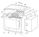
図11は素子基板を複数個、記録幅方向に一列に配列して形成するフルライン記録ヘッドの構成を示す図である。 FIG. 11 is a diagram showing a configuration of a full-line recording head formed by arranging a plurality of element substrates in a line in the recording width direction.
図11に示されるように、平行四辺形の形状をした各素子基板502は複数の記録素子列504を備え、各信号及び電源は記録装置(不図示)からコネクタ503とヘッド配線506とを介して電極パッド505へと供給される。また、素子基板502を一列に連結して並べる(この例では4個)ことにより、記録ヘッド501の1辺のサイズ(H)を小さくすることができる。各素子基板502のつなぎ部分は記録幅方向(W)に対して角度を持った形状をしており、複数の素子基板502を近接して配置できるため、素子基板502のつなぎ部で重複して配置する記録素子数を低減することができる。なお、素子基板502を一列に連結して並べるためには、電極パッド505は記録素子列504と並行に各素子基板の端部付近に配置することが必要となる。
As shown in FIG. 11, each
図12は素子基板を複数個、記録幅方向に千鳥状に並べて形成するフルライン記録ヘッドの構成を示す図である。なお、図12において、図11と重複する部分は同じ参照番号を付し、その説明を省略する。 FIG. 12 is a diagram showing a configuration of a full-line recording head in which a plurality of element substrates are arranged in a staggered pattern in the recording width direction. In FIG. 12, the same parts as those in FIG.
良好な吐出特性を得るためには素子基板502を千鳥状に並べる構成においても隣接する素子基板を近接して配置することが必要である。記録素子列504の方向とは垂直方向に電極パッド505を配列する構成では、電極パッド505からコネクタ503へのヘッド配線のための領域が確保できない。このため、図12に示すように、千鳥状に素子基板を並べる構成でも電極パッド505を記録素子列504と並行に配置することが必要である。
In order to obtain good ejection characteristics, it is necessary to arrange adjacent element substrates close to each other even in a configuration in which the
以上のように、電極パッドを記録素子列と並行に配列する構成では、インクを記録素子に個別に供給するインク供給口の間を通って電源配線を配置することにより、電源配線長を短くすることができる。このようにして、素子基板内部での電源配線抵抗による電圧降下を低減することにより、高品位な記録の高速化を実現し、記録ヘッドそのものの耐久性を高めることが可能となる。 As described above, in the configuration in which the electrode pads are arranged in parallel with the printing element array, the power wiring is shortened by arranging the power wiring through the ink supply ports that individually supply ink to the printing elements. be able to. In this way, by reducing the voltage drop due to the power supply wiring resistance inside the element substrate, it is possible to realize high-quality recording at high speed and enhance the durability of the recording head itself.
しかしながらインク供給口間の距離は記録素子を配置するピッチに依存するため、特許文献1が提案するように電源配線を複数に分割して配線抵抗を合せ込むことができない。そのため記録素子までの電源配線抵抗が記録素子列毎に異なってしまい、対応する記録素子に印加される電圧に差が生じてしまうという問題がある。 However, since the distance between the ink supply ports depends on the pitch at which the recording elements are arranged, as proposed in Patent Document 1, it is impossible to divide the power supply wiring into a plurality of pieces and match the wiring resistance. For this reason, there is a problem in that the power supply wiring resistance to the recording element differs for each recording element array, and a difference occurs in the voltage applied to the corresponding recording element.
本発明は上記従来例に鑑みてなされたもので、配線抵抗の差による影響をなくし、駆動されるヒータに印加される電圧を一定にすることが可能な素子基板、液体吐出ヘッド及び記録装置を提供すること目的としている。 The present invention has been made in view of the above-described conventional example. An element substrate, a liquid discharge head, and a recording apparatus that can eliminate the influence of the difference in wiring resistance and can make the voltage applied to the driven heater constant. The purpose is to provide.
上記目的を達成するために本発明の素子基板は次のような構成からなる。 In order to achieve the above object, the element substrate of the present invention has the following configuration.
即ち、複数のヒータを配列して形成するヒータ列を並列に配置してなる複数のヒータ列と、前記複数のヒータ列に含まれる前記複数のヒータに対応し前記複数のヒータを駆動する複数のトランジスタと、前記複数のヒータに印加する電圧を供給する第1の電極パッドと、前記複数のヒータを接地する第2の電極パッドと、前記第1の電極パッドと前記複数のヒータとを接続する第1の配線と、前記複数のヒータと前記第2の電極パッドとを接続する第2の配線を備える素子基板であって、前記第1の電極パッドと前記第2の電極パッドとは、前記複数のヒータの配列方向に沿って設けられており、前記複数のヒータ列の内、前記第1の電極パッド及び前記第2の電極パッドとの間隔が相対的に大きい位置に設けられるヒータ列に含まれる前記複数のヒータを駆動する複数の第1のトランジスタのサイズが、前記第1の電極パッド及び前記第2の電極パッドとの間隔が相対的に小さい位置に設けられるヒータ列に含まれる前記複数のヒータを駆動する複数の第2のトランジスタのサイズより大きく、前記素子基板は、前記複数のヒータに対応して設けられ、対応する前記複数のヒータに液体を供給するための複数の供給口をさらに備え、前記第1の配線の少なくとも一部と前記第2の配線の少なくとも一部とは前記複数の供給口の間を通り格子状に形成され、前記複数のヒータに接続されること、又は、前記複数のヒータ列に含まれる前記複数のヒータはヒータ列ごとに複数のグループに分割され、該分割されたグループに対応して前記第1の電極パッドと前記第1の配線と前記第2の電極パッドと前記第2の配線とがそれぞれ複数、設けられ、前記複数の第1の配線と前記複数の第2の配線とが前記対応するグループに含まれるヒータに接続されること、又は、前記複数のヒータ列それぞれに含まれる複数のヒータが配列される方向に、前記対応する複数のトランジスタのサイズが異なること、又は、前記素子基板の形状は平行四辺形であり、前記複数の第1のトランジスタのサイズに関し、前記平行四辺形の鋭角部の端部の近くに設けられるトランジスタのサイズは前記鋭角部の端部の近くに設けられないトランジスタのサイズより大きいことを特徴とする。
あるいは、複数のヒータを配列して形成するヒータ列を並列に配置してなる複数のヒータ列と、前記複数のヒータ列に含まれる前記複数のヒータに対応し前記複数のヒータを駆動する複数のトランジスタと、前記複数のヒータに印加する電圧を供給する第1の電極パッドと、前記複数のヒータを接地する第2の電極パッドと、前記第1の電極パッドと前記複数のヒータとを接続する第1の配線と、前記複数のヒータと前記第2の電極パッドとを接続する第2の配線を備える素子基板であって、前記複数のヒータ列の内、前記第1の配線における前記第1の電極パッドと前記複数のヒータとの間の電気抵抗と前記第2の配線における前記第2の電極パッドと前記複数のヒータとの間の電気抵抗の合計が相対的に大きいヒータ列に含まれる前記複数のヒータを駆動する複数の第1のトランジスタのサイズが、前記第1の配線における前記第1の電極パッドと前記複数のヒータとの間の電気抵抗と前記第2の配線における前記第2の電極パッドと前記複数のヒータとの間の電気抵抗の合計が相対的に小さいヒータ列に含まれる前記複数のヒータを駆動する複数の第2のトランジスタのサイズより大きく、前記素子基板は、前記複数のヒータに対応して設けられ、対応する前記複数のヒータに液体を供給するための複数の供給口をさらに備え、前記第1の配線の少なくとも一部と前記第2の配線の少なくとも一部とは前記複数の供給口の間を通り格子状に形成され、前記複数のヒータに接続されることを特徴としても良い。
That is, a plurality of heater rows formed by arranging a plurality of heaters in parallel and a plurality of heater rows corresponding to the plurality of heaters included in the plurality of heater rows are driven. A transistor, a first electrode pad for supplying a voltage to be applied to the plurality of heaters, a second electrode pad for grounding the plurality of heaters, and the first electrode pad and the plurality of heaters are connected. An element substrate including a first wiring and a second wiring for connecting the plurality of heaters and the second electrode pad, wherein the first electrode pad and the second electrode pad are A heater array provided along the arrangement direction of the plurality of heaters, the heater array provided at a position where the distance between the first electrode pad and the second electrode pad is relatively large among the plurality of heater arrays. Included The plurality of heaters included in a heater row provided with a size of a plurality of first transistors driving a plurality of heaters at a position where a distance between the first electrode pad and the second electrode pad is relatively small rather larger than the size of the plurality of second transistors for driving the said element substrate, the plurality of heaters provided in correspondence, a plurality of supply ports for supplying liquid to a corresponding plurality of heaters further At least a part of the first wiring and at least a part of the second wiring are formed in a lattice shape between the plurality of supply ports and connected to the plurality of heaters, or The plurality of heaters included in the plurality of heater arrays are divided into a plurality of groups for each heater array, and the first electrode pad, the first wiring, and the second are corresponding to the divided groups. A plurality of electrode pads and a plurality of second wirings are provided, and the plurality of first wirings and the plurality of second wirings are connected to heaters included in the corresponding group, or The size of the corresponding plurality of transistors is different in the direction in which the plurality of heaters included in each of the plurality of heater arrays is arranged, or the shape of the element substrate is a parallelogram, and the plurality of first Regarding the size of the transistor, the size of the transistor provided near the end of the acute angle portion of the parallelogram is larger than the size of the transistor not provided near the end of the acute angle portion .
Alternatively, a plurality of heater rows formed by arranging a plurality of heaters in parallel and a plurality of heater rows corresponding to the plurality of heaters included in the plurality of heater rows are driven. A transistor, a first electrode pad for supplying a voltage to be applied to the plurality of heaters, a second electrode pad for grounding the plurality of heaters, and the first electrode pad and the plurality of heaters are connected. An element substrate comprising a first wiring and a second wiring for connecting the plurality of heaters and the second electrode pad, wherein the first wiring in the first wiring in the plurality of heater arrays. The total of the electrical resistance between the electrode pad and the plurality of heaters and the electrical resistance between the second electrode pad and the plurality of heaters in the second wiring are included in the heater row that is relatively large. Said compound The size of the plurality of first transistors for driving the heaters is such that the electrical resistance between the first electrode pad and the plurality of heaters in the first wiring and the second electrode in the second wiring pad and rather larger than the size of the plurality of second transistors total electrical resistance for driving the plurality of heaters included in relatively small heater array between the plurality of heaters, the element substrate, the plurality A plurality of supply ports for supplying liquid to the corresponding plurality of heaters, and at least a part of the first wiring and at least a part of the second wiring. May be formed in a lattice pattern between the plurality of supply ports and connected to the plurality of heaters .
また本発明を別の側面から見れば、上記構成の素子基板を実装し、液体を吐出するヘッドを構成することを特徴とする液体吐出ヘッドを、特にインクを吐出して記録を行うインクジェット記録ヘッドとして構成し、さらには上記構成の素子基板を複数、前記複数のヒータの配列の方向に配置して記録媒体の幅に対応した記録幅としたフルライン記録ヘッドを備える。 According to another aspect of the present invention, there is provided a liquid discharge head, in which an element substrate having the above-described structure is mounted and a liquid discharge head is formed. And a full line recording head having a recording width corresponding to the width of the recording medium by arranging a plurality of element substrates configured as described above in the direction of the arrangement of the plurality of heaters.
さらに本発明を別の側面から見れば、上記インクジェット記録ヘッド又はフルライン記録ヘッドを用いて記録を行う記録装置を備える。 Further, from another aspect, the present invention includes a recording apparatus that performs recording using the ink jet recording head or the full line recording head.
従って本発明によれば、素子基板内で配線抵抗が異なることによる電圧変化をなくし、ヒータに印加される電圧を一定にすることができるという効果がある。また、配線抵抗が小さい場所に位置する記録素子のトランジスタのサイズを小さく、配線抵抗が大きい場所に位置する記録素子のトランジスタのサイズを大きくすることにより、素子基板のサイズを削減することができる。 Therefore, according to the present invention, there is an effect that the voltage change due to the different wiring resistance in the element substrate can be eliminated, and the voltage applied to the heater can be made constant. Also, the size of the element substrate can be reduced by reducing the size of the transistor of the recording element located in the place where the wiring resistance is low and increasing the size of the transistor of the recording element located in the place where the wiring resistance is high.
なお、この素子基板が記録ヘッドとして用いられるなら、記録画像の画質が向上するという効果もある。 If this element substrate is used as a recording head, the image quality of the recorded image can be improved.
以下添付図面を参照して本発明の好適な実施例について、さらに具体的かつ詳細に説明する。ただし、この実施例に記載されている構成要素の相対配置等は、特定の記載がない限りは、この発明の範囲をそれらのみに限定する趣旨のものではない。 Hereinafter, preferred embodiments of the present invention will be described more specifically and in detail with reference to the accompanying drawings. However, the relative arrangement and the like of the constituent elements described in this embodiment are not intended to limit the scope of the present invention only to those unless otherwise specified.
なお、この明細書において、「記録」(「プリント」という場合もある)とは、文字、図形等有意の情報を形成する場合のみならず、有意無意を問わない。さらに人間が視覚で知覚し得るように顕在化したものであるか否かも問わず、広く記録媒体上に画像、模様、パターン等を形成する、または媒体の加工を行う場合も表すものとする。 In this specification, “recording” (sometimes referred to as “printing”) is not limited to the case of forming significant information such as characters and graphics, but may be significant. Furthermore, it also represents a case where an image, a pattern, a pattern, or the like is widely formed on a recording medium or a medium is processed regardless of whether or not it is manifested so that a human can perceive it visually.
また、「記録媒体」とは、一般的な記録装置で用いられる紙のみならず、広く、布、プラスチック・フィルム、金属板、ガラス、セラミックス、木材、皮革等、インクを受容可能なものも表すものとする。 “Recording medium” refers not only to paper used in general recording apparatuses but also widely to cloth, plastic film, metal plate, glass, ceramics, wood, leather, and the like that can accept ink. Shall.
さらに、「インク」(「液体」と言う場合もある)とは、上記「記録(プリント)」の定義と同様広く解釈されるべきものである。従って、記録媒体上に付与されることによって、画像、模様、パターン等の形成または記録媒体の加工、或いはインクの処理(例えば記録媒体に付与されるインク中の色剤の凝固または不溶化)に供され得る液体を表すものとする。 Further, “ink” (sometimes referred to as “liquid”) should be interpreted widely as in the definition of “recording (printing)”. Therefore, by being applied on the recording medium, it is used for formation of images, patterns, patterns, etc., processing of the recording medium, or ink processing (for example, solidification or insolubilization of colorant in the ink applied to the recording medium). It shall represent a liquid that can be made.
またさらに、「記録要素」とは、特にことわらない限り吐出口ないしこれに連通する液路およびインク吐出に利用されるエネルギーを発生する素子を総括して言うものとする。 Furthermore, unless otherwise specified, the “recording element” collectively refers to an ejection port or a liquid path communicating with the ejection port and an element that generates energy used for ink ejection.
本発明の最も重要な特徴をなすインクジェット記録ヘッド(以下、記録ヘッド)は、記録ヘッドの素子基板に複数の記録素子とこれら記録素子を駆動する駆動回路とを同一基板に実装している。後述の説明から分かるように、記録ヘッドには複数の素子基板を内蔵し、これらの素子基板をカスケード接続する構造をとっている。従って、この記録ヘッドは相対的に長い記録幅を達成することができる。従って、その記録ヘッドは一般に見られるシリアルタイプの記録装置のみならず、その記録幅が記録媒体の幅に相当するようなフルライン記録ヘッドを備えた記録装置に用いられる。また、その記録ヘッドはシリアルタイプの記録装置の中でも、A0やB0などの大きなサイズの記録媒体を用いる大判プリンタに用いられる。 An ink jet recording head (hereinafter referred to as a recording head) which constitutes the most important feature of the present invention has a plurality of recording elements and a drive circuit for driving these recording elements mounted on the same substrate. As will be understood from the following description, the recording head has a structure in which a plurality of element substrates are built in and these element substrates are cascade-connected. Therefore, this recording head can achieve a relatively long recording width. Therefore, the recording head is used not only for a serial type recording apparatus commonly found, but also for a recording apparatus having a full line recording head whose recording width corresponds to the width of the recording medium. Further, the recording head is used in a large format printer using a recording medium having a large size such as A0 or B0 among serial type recording apparatuses.
従って、まず本発明の記録ヘッドが用いられる記録装置について説明する。 Accordingly, first, a recording apparatus using the recording head of the present invention will be described.
<フルライン記録ヘッドを搭載した記録装置(図1)>
図1はフルラインのインクジェット記録ヘッド(以下、記録ヘッド)11K、11C、11M、11Yと常に安定したインク吐出を保証するための回復系ユニットを備えた記録装置1の構造を説明するための斜視透視図である。
<Recording device equipped with a full-line recording head (FIG. 1)>
FIG. 1 is a perspective view for explaining the structure of a recording apparatus 1 including full-line inkjet recording heads (hereinafter referred to as recording heads) 11K, 11C, 11M, and 11Y and a recovery system unit that guarantees stable ink ejection at all times. FIG.
記録装置1において、記録用紙15は、フィーダユニット17から、これら記録ヘッドによる印刷位置に供給され、記録装置の筐体18に具備された搬送ユニット16によって搬送される。
In the recording apparatus 1, the
記録用紙15への画像の印刷は、記録用紙15を搬送しながら、記録用紙15の基準位置がブラック(K)インクを吐出する記録ヘッド11Kの下に到達したときに、記録ヘッド11Kからブラックインクを吐出する。同様に、シアン(C)インクを吐出する記録ヘッド11C、マゼンタ(M)インクを吐出する記録ヘッド11M、イエロ(Y)インクを吐出する記録ヘッド11Yの順に、各基準位置に記録用紙15が到達すると各色のインクを吐出してカラー画像が形成される。こうして画像が印刷された記録用紙15はスタッカトレイ20に排出されて堆積される。
The printing of the image on the
記録装置1は、更に搬送ユニット16、記録ヘッド11K、11C、11M、11Yにインクを供給するための各インク毎に交換可能なインクカートリッジ(不図示)を有している。またさらに、記録ヘッド11K、11C、11M、11Yへのインク供給や回復動作のためのポンプユニット(不図示)、記録装置1全体を制御する制御基板(不図示)等を有している。またフロントドア19は、インクカートリッジの交換用の開閉扉である。
The recording apparatus 1 further includes a replaceable ink cartridge (not shown) for supplying ink to the
<大判の記録媒体を用いる記録装置(図2)>
図2はA0やB0サイズの記録媒体を用いる記録装置の外観斜視図であり、図2(b)は図2(a)に示した記録装置のアッパカバーを取り外した状態を示す斜視図である。
<Recording device using large format recording medium (FIG. 2)>
FIG. 2 is an external perspective view of a recording apparatus using a recording medium of A0 or B0 size, and FIG. 2B is a perspective view showing a state in which the upper cover of the recording apparatus shown in FIG. .
図2(a)に示されるように、記録装置2の前面に手差し挿入口88が設けられ、その下部に前面へ開閉可能なロール紙カセット89が設けられており、記録紙等の記録媒体は手差し挿入口88又はロール紙カセット89から記録装置内部へと供給される。記録装置2は、2個の脚部93に支持された装置本体94、排紙された記録媒体を積載するスタッカ90、内部が透視可能な透明で開閉可能なアッパカバー91を備えている。また、装置本体94の右側には、操作パネル12、インク供給ユニット及びインクタンクが配設されている。
As shown in FIG. 2 (a), a manual insertion slot 88 is provided on the front surface of the
図2(b)に示されているように、記録装置2はさらに、記録媒体を矢印B方向(副走査方向)に搬送するための搬送ローラ70と、記録媒体の幅方向(矢印A方向、主走査方向)に往復移動可能に案内支持されたキャリッジ4とを備えている。記録装置2はさらに、キャリッジ4を矢印A方向に往復移動させるためのキャリッジモータ(不図示)とキャリッジベルト(以下、ベルト)270と、キャリッジ4に装着された記録ヘッド11とを備えている。またさらに、インクを供給するとともに記録ヘッド11の吐出口の目詰まりなどによるインク吐出不良を解消させるための吸引式インク回復ユニット9も備えられている。
As shown in FIG. 2B, the
この記録装置の場合、キャリッジ4には、記録媒体にカラー記録を行うために、4つのカラーインクに対応して4つのヘッドからなる記録ヘッド11が装着されている。即ち、記録ヘッド11は、例えば、K(ブラック)インクを吐出するKヘッド、C(シアン)インクを吐出するCヘッド、M(マゼンタ)インクを吐出するMヘッド、Y(イエロ)インクを吐出するYヘッドで構成されている。
In the case of this recording apparatus, a
以上の構成で記録媒体に記録を行う場合、搬送ローラ70によって記録媒体を所定の記録開始位置まで搬送する。その後、キャリッジ4により記録ヘッド11を主走査方向に走査させる動作と、搬送ローラ70により記録媒体を副走査方向に搬送させる動作とを繰り返すことにより、記録媒体全体に対する記録が行われる。
When recording on the recording medium with the above configuration, the recording medium is transported to a predetermined recording start position by the
即ち、ベルト270およびキャリッジモータ(不図示)によってキャリッジ4が図2(b)に示された矢印A方向に移動することにより、記録媒体に記録が行われる。キャリッジ4が走査される前の位置(ホームポジション)に戻されると、搬送ローラによって記録媒体が副走査方向(図2(b)に示された矢印B方向)に搬送され、その後、再び図2中の矢印A方向にキャリッジを走査する。このようにして、記録媒体に対する画像や文字等の記録が行なわれる。さらに上記の動作を繰り返し、記録媒体の1枚分の記録が終了すると、その記録媒体はスタッカ90内に排紙され、1枚分の記録が完了する。
That is, recording is performed on the recording medium by moving the
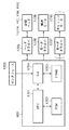
<制御構成の説明(図3)>
次に、図1〜図2を用いて説明した記録装置の記録制御を実行するための制御構成について説明する。
<Description of control configuration (FIG. 3)>
Next, a control configuration for executing recording control of the recording apparatus described with reference to FIGS.
図3は記録装置の制御回路の構成を示すブロック図である。図3において、1700は記録データを入力するインタフェース、1701はMPU、1702はMPU1701が実行する制御プログラムを格納するROM、1703は記録データや記録ヘッドに供給される記録信号等のデータを保存しておくDRAMである。1704は記録ヘッドに対する記録信号の供給制御を行うゲートアレイ(G.A.)であり、インタフェース1700、MPU1701、DRAM1703間のデータ転送制御も行う。コントローラ600は、MPU1701、ROM1702、DRAM1703、ゲートアレイ1704を備えている。1710は記録ヘッド11(11K、11C、11M、11Y)を搬送するためのキャリッジモータ、1709は記録紙搬送のための搬送モータである。1705は記録ヘッドを駆動するヘッドドライバ、1706、1707はそれぞれ搬送モータ1709、キャリッジモータ1710を駆動するためのモータドライバである。
FIG. 3 is a block diagram showing the configuration of the control circuit of the recording apparatus. In FIG. 3, 1700 is an interface for inputting recording data, 1701 is an MPU, 1702 is a ROM for storing a control program executed by the
なお、図1に示すようなフルライン記録ヘッドを用いる構成の記録装置では、キャリッジモータ1710やそのモータを駆動するモータドライバ1707は存在しない。このために、図3ではカッコ符号をつけた。
In the recording apparatus using the full line recording head as shown in FIG. 1, the
上記制御構成の動作を説明すると、インタフェース1700に記録データが入るとゲートアレイ1704とMPU1701との間で記録データが記録用の記録信号に変換される。そして、モータドライバ1706、1707が駆動されると共に、ヘッドドライバ1705に送られた記録データに従って記録ヘッドが駆動され、記録が行われる。また、記録ヘッドで得られた転送エラー(後述)の情報はヘッドドライバ1705を介してMPU1701にフィードバックされ、記録制御に反映される。
The operation of the above control configuration will be described. When recording data enters the
<記録素子の駆動原理(図4)>
図4は記録素子及び記録素子を駆動する駆動回路として動作するトランジスタとを含む回路構成図である。
<Driving Principle of Recording Element (FIG. 4)>
FIG. 4 is a circuit configuration diagram including a recording element and a transistor that operates as a drive circuit for driving the recording element.
図4に示されるように、記録素子列402はm×n個の記録素子から構成され、n個毎にm個のグループ409−1から409−mに分割される。また、各記録素子402−ijのグランド側はNMOS408−ijと接続している。ここで、i=1〜m、j=1〜nである。従って、図4に示す構成において、iグループのj番目の記録素子とNMOSとはそれぞれ、402−ij、408−ijと一般的に表記できる。
As shown in FIG. 4, the
グループmのNMOS408−m1〜408mnのソースは共通のグランド配線407−mに接続する。また、グランド(接地)の電極パッド405の近傍でグランド配線407−1〜407−mは結線されグランド配線407となり電極パッド405と電気的に接続する。一方、グループmの記録素子402−m1〜mnは電源配線406−mと接続され、電極パッド404の近傍で電源配線406−1〜406−mは結線され電源配線406となり外部から電力を供給するための電極パッド404と電気的に接続する。
The sources of the NMOSs 408-m1 to 408mn of the group m are connected to the common ground wiring 407-m. Further, the ground wirings 407-1 to 407-m are connected in the vicinity of the ground (ground)
記録装置(不図示)から記録データが送信され、NMOS408−ijのゲートに駆動電圧が印加されるとの記録素子402−ijに電流が流れ、インクに熱エネルギーを与えインクが吐出口から吐出される。同じグループの記録素子は1つのブロック時間に同時に1つまでの駆動とする時分割駆動により、電源配線406及びグランド配線407での電圧降下は同時駆動数に係わらず一定となる。
When recording data is transmitted from a recording device (not shown) and a driving voltage is applied to the gate of the NMOS 408-ij, a current flows through the recording element 402-ij, giving thermal energy to the ink, and the ink is ejected from the ejection port. The The voltage drops in the
また、NMOS408−ijのソースを電源電圧と接続したソースフォロワ構成ではNMOS408−ijのゲートに駆動電圧が印加されると、記録素子が駆動される。また、記録素子の両側にNMOSとPMOSを配置する構成では両方のトランジスタのゲートに駆動電圧が印加されると、記録素子が駆動される。 In the source follower configuration in which the source of the NMOS 408-ij is connected to the power supply voltage, the recording element is driven when a driving voltage is applied to the gate of the NMOS 408-ij. In the configuration in which NMOS and PMOS are arranged on both sides of the recording element, the recording element is driven when a driving voltage is applied to the gates of both transistors.
以下説明する実施列では図4に示す回路構成に基づいて説明するが、記録素子の駆動回路構成はここで説明した限りではない。 In the embodiments described below, description will be made based on the circuit configuration shown in FIG. 4, but the drive circuit configuration of the recording element is not limited to that described here.
次に、以上の構成に記録装置に搭載される記録ヘッドの素子基板についての幾つかの実施例について説明する。 Next, several embodiments of the element substrate of the recording head mounted on the recording apparatus with the above configuration will be described.
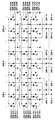
図5は実施例1に従う素子基板101を示す図である。図6は実施例1に従う駆動回路の構成を示す図である。図5〜図6に示す構成では、互いに並列に配置されるk個の記録素子列があり、各記録素子列にはm×n個の記録素子が含まれ、記録素子がマトリクス状に形成される。また、これらの記録素子に対応して、これらの記録素子を駆動するNMOSトランジスタもマトリクス状に形成される。そして、各記録素子列の記録素子は記録装置の記録解像度の間隔(例えば、600dpi)で配列され、近接するn個毎の記録素子でm個のグループ109−1〜mに分割されている。そして、各グループから最大1個の記録素子が選択されて時分割駆動される。
FIG. 5 shows the
実施例1の構成ではk列目のmグループのn番目の記録素子を102−kmnと表す。従って、一般的には任意の記録素子は102−hijと表記され、h=1〜k、i=1〜m、j=1〜nである。この実施例では記録素子102−km1について説明する。 In the configuration of the first embodiment, the n-th recording element in the m-th group in the k-th column is represented as 102-kmn. Therefore, generally, an arbitrary recording element is expressed as 102-hij, and h = 1 to k, i = 1 to m, and j = 1 to n. In this embodiment, the recording element 102-km1 will be described.
記録素子102−km1に対応して1つのインク供給口103−km1が形成され、共通流路(不図示)よりインクを供給する。電源電圧は電極パッド104−mから電源配線106−mを経て記録素子102−km1に供給される。電源配線106−mはインク供給口103−1m1と103−1m2との間からインク供給口103−km1と103−km2との間を通って複数の列(h=1〜k)の記録素子間で共通に接続される。グランド電圧も同様に、電極パッド105−mからグランド配線107−mを経てトランジスタ108−km1に接続される。グランド配線107−mはインク供給口103−1(m−1)nと103−1m1との間からインク供給口103−k(m−1)nと103−km1との間を通って複数の列(h=1〜k)に渡って共通に接続される。同じグループの電源配線106−m及びグランド配線107−mは対応するパッド付近で結線されている。このようにパッド付近で複数の配線を結線することにより共通配線での抵抗値は無視できる程小さくなる。 One ink supply port 103-km1 is formed corresponding to the recording element 102-km1, and ink is supplied from a common flow path (not shown). The power supply voltage is supplied from the electrode pad 104-m to the recording element 102-km1 through the power supply wiring 106-m. The power supply wiring 106-m passes between the ink supply ports 103-km1 and 103-km2 from between the ink supply ports 103-1m1 and 103-1m2, and between the printing elements in a plurality of rows (h = 1 to k). Connected in common. Similarly, the ground voltage is connected from the electrode pad 105-m to the transistor 108-km1 through the ground wiring 107-m. The ground wiring 107-m passes between the ink supply ports 103-1 (m-1) n and 103-1m1 and between the ink supply ports 103-k (m-1) n and 103-km1. They are connected in common across the columns (h = 1 to k). The power supply wiring 106-m and the ground wiring 107-m of the same group are connected in the vicinity of the corresponding pads. In this way, by connecting a plurality of wirings in the vicinity of the pad, the resistance value in the common wiring becomes so small that it can be ignored.
トランジスタ108−km1のゲートに駆動電源が印加されると記録素子102−km1に電流が流れ発熱し、インクが吐出口(不図示)より吐出される。複数の記録素子の同時駆動により電圧降下に差が生じることを避けるため、列間で共通に接続された記録素子(例えば、102−1m1〜102−km1)は同時駆動しないよう時分割駆動する。なお、インク供給口は1つの記録素子に対し2つのインク供給口を形成しても良く、図5に示す構成によって限定されるものではない。 When driving power is applied to the gate of the transistor 108-km1, a current flows through the recording element 102-km1, heat is generated, and ink is ejected from an ejection port (not shown). In order to avoid a difference in voltage drop due to simultaneous driving of a plurality of recording elements, the recording elements (for example, 102-1m1 to 102-km1) connected in common between the columns are time-division driven so as not to be simultaneously driven. The ink supply port may form two ink supply ports for one recording element, and is not limited to the configuration shown in FIG.
図5に示す構成では列間で共通の電源配線106−i(i=1〜m)で記録素子102−hijを接続しているため、電源電圧の電極パッド104−i(i=1〜m)から記録素子102−hijまでの配線抵抗に差が生じる。記録素子102−km1の電源配線の抵抗は電源配線106−1m1〜106−km1の合計であるのに対し、記録素子102−1m1の電源配線の抵抗は電源配線106−1m1のみである。グランドも同様に列間で共通のグランド配線107−i(i=1〜m)でトランジスタ108−hijと接続しているため、グランドの電極パッド105−i(i=1〜m)からトランジスタ108−hijまでの配線抵抗に差が生じる。
In the configuration shown in FIG. 5, since the recording elements 102-hij are connected by common power supply wirings 106-i (i = 1 to m) between the columns, the power supply voltage electrode pads 104-i (i = 1 to m). ) To the recording element 102-hij. The resistance of the power supply wiring of the recording element 102-km1 is the sum of the power supply wirings 106-1m1 to 106-km1, whereas the resistance of the power supply wiring of the recording element 102-1m1 is only the power supply wiring 106-1m1. Similarly, since the ground is connected to the transistor 108-hij through the common ground wiring 107-i (i = 1 to m) between the columns, the
図7は電源電圧に対する各素子に係る電圧内訳を示す図であり、図7(a)は従来例を示し、図7(b)はこの実施例に従う例を示している。 FIG. 7 is a diagram showing a breakdown of voltages related to each element with respect to the power supply voltage. FIG. 7 (a) shows a conventional example, and FIG. 7 (b) shows an example according to this embodiment.
図7(a)に示すように、従来例によれば、電極パッドから離れている記録素子102−km1では配線抵抗が大きく、記録素子に印加される電圧が小さくなる。一方、電極パッドに近い記録素子102−1m1では配線抵抗が小さく、記録素子に印加される電圧が大きくなる。このように従来例によれば、記録素子に印加される電圧が列間で異なり、その結果、吐出特性が変化してしまう。 As shown in FIG. 7A, according to the conventional example, in the recording element 102-km1 that is away from the electrode pad, the wiring resistance is large, and the voltage applied to the recording element is small. On the other hand, in the recording element 102-1m1 close to the electrode pad, the wiring resistance is small, and the voltage applied to the recording element is large. As described above, according to the conventional example, the voltage applied to the printing element differs between the columns, and as a result, the ejection characteristics change.
これに対して、この実施例によれば、図5に示すように、電極パッドまでの配線抵抗(電源配線とグランド配線の和)が小さい記録素子を駆動するトランジスタの面積を小さく形成する。具体的には、記録素子102−km1に対しては従来例と同じく駆動に必要なトランジスタ108−km1の面積を維持する一方、記録素子102−1m1に対してはトランジスタ108−1m1の面積を小さくする。トランジスタの面積を小さくするとオン抵抗が大きくなるため、記録素子に印加される電圧はその分小さくなる。このようにして、記録素子列間での配線抵抗の差をトランジスタの面積を変えたことによるオン抵抗の増加分で合せ込みを行う。 On the other hand, according to this embodiment, as shown in FIG. 5, the area of the transistor for driving the recording element having a small wiring resistance to the electrode pad (the sum of the power supply wiring and the ground wiring) is formed small. Specifically, the area of the transistor 108-km1 necessary for driving is maintained for the recording element 102-km1 as in the conventional example, while the area of the transistor 108-1m1 is small for the recording element 102-1m1. To do. When the area of the transistor is reduced, the on-resistance is increased, so that the voltage applied to the recording element is reduced accordingly. In this way, the difference in the wiring resistance between the recording element arrays is matched with the increase in the on-resistance due to the change in the area of the transistor.
図5に示されるように、この実施例では記録素子列の方向にトランジスタのサイズを変化させている。具体的には、記録素子列の方向に関し、第k列のトランジスタのサイズをHk、……、第2列のトランジスタのサイズをH2、第1列のトランジスタのサイズをH1とすれば、Hk>……>H2>H1である。このように、電極パッドからの距離が遠いほどトランジスタのサイズが大きくなり、トランジスタの面積が大きくなる。 As shown in FIG. 5, in this embodiment, the size of the transistor is changed in the direction of the printing element array. Specifically, regarding the direction of the printing element array, if the size of the k-th column transistor is Hk,..., The second column transistor size is H2, and the first column transistor size is H1, Hk> ...> H2> H1. Thus, as the distance from the electrode pad increases, the size of the transistor increases and the area of the transistor increases.
従って以上説明した実施例に従えば、図7(b)に示される記録素子102−km1と記録素子102−1m1に印加される電圧を比較すると分かるように、電極パッドからの配線抵抗値に応じて記録素子列間で記録素子への印加電圧を一定にすることができる。これにより、記録素子内で安定した吐出特性を得ることができる。また、トランジスタの面積を変化させる際に記録素子列の方向に小さくすることで、電極パッドから記録素子への配線長が短くなるので配線抵抗値を低減することができ、素子基板幅の短縮化も可能となる。 Therefore, according to the embodiment described above, the voltage applied to the recording element 102-1m1 and the recording element 102-1m1 shown in FIG. Thus, the voltage applied to the recording elements can be made constant between the recording element arrays. Thereby, stable ejection characteristics can be obtained in the recording element. In addition, by reducing the area of the transistor in the direction of the recording element array, the wiring length from the electrode pad to the recording element is shortened, so that the wiring resistance value can be reduced and the element substrate width is shortened. Is also possible.
なお、この実施例では、多層構造の素子基板を用い、トランジスタをAlで第1層、グランド配線をAlで第2層、電源配線をAlで第3層に形成しているが、途中でスルーホールを介して同じ層で配線を形成しても構わない。また、電極パッドは素子基板の片側だけではなく両側に配列されていても構わない。その場合も電極パッドからの抵抗値に応じてトランジスタの面積を変化させることで、記録素子への印加電圧を一定にすることができる。 In this embodiment, an element substrate having a multilayer structure is used, the transistor is formed of Al in the first layer, the ground wiring is formed of Al in the second layer, and the power supply wiring is formed of Al in the third layer. You may form wiring with the same layer through a hole. Further, the electrode pads may be arranged not only on one side of the element substrate but also on both sides. Also in that case, the voltage applied to the recording element can be made constant by changing the area of the transistor in accordance with the resistance value from the electrode pad.
図8は実施例2に従う素子基板を示す図である。図9は実施例2に従う駆動回路構成を示す図である。図8〜図9を実施例1で説明した図5〜図6に示す構成と比較すると配線のみが異なっており、その他の配置や構成要素は同じである。従って、図8〜図9に記載の共通の構成要素についての説明は省略し、その参照番号のみを実施例1では1xx−yyyと記載していたのを実施例2では2xx−yyyと記載して、その構成要素が実施例2に係るものであることを示す。 FIG. 8 is a view showing an element substrate according to the second embodiment. FIG. 9 is a diagram showing a drive circuit configuration according to the second embodiment. 8 to 9 are different from the configuration shown in FIGS. 5 to 6 described in the first embodiment, only the wiring is different, and the other arrangements and components are the same. Accordingly, the description of the common components described in FIGS. 8 to 9 is omitted, and only the reference number is described as 1xx-yyy in the first embodiment, but is described as 2xx-yyy in the second embodiment. Thus, it is shown that the constituent elements are those according to the second embodiment.
実施例2では電源配線206とグランド配線207とは素子基板201内の全ての記録素子に接続するように、記録素子202−hijとインク供給口203−hijの間を格子状に接続されている。これにより、例えば、記録素子列だけが異なる記録素子202−k11と202−211とが同時駆動されたとしても配線が格子状に接続されているので電流が集中せず、電流は抵抗の低い方へと分散される。また、電極パッド204−1〜204−m、グランドパッド205−1〜205−mも電源配線206及びグランド配線207を通して共通に接続されている。これにより、同時駆動数が記録素子列の方向に変化しても電流が分散されるので、配線抵抗による電圧降下は変化しない。
In the second embodiment, the
従って以上説明した実施例に従えば、配線構成でトランジスタ208−k11からトランジスタ208−111に徐々にその面積を小さくするので、記録素子列間で記録素子への印加電圧を一定にし、記録素子で安定した吐出特性を得ることができる。また、トランジスタの面積を変化させる際に記録素子列の方向に素子基板のサイズを小さくすることで、電極パッドから記録素子への配線長が短くして配線抵抗値を低減することができ、素子基板のサイズを削減することも可能となる。 Therefore, according to the embodiment described above, the area of the transistor 208-k11 to the transistor 208-111 is gradually reduced in the wiring configuration, so that the voltage applied to the recording elements is made constant between the recording element arrays. Stable ejection characteristics can be obtained. Further, by reducing the size of the element substrate in the direction of the recording element array when changing the area of the transistor, the wiring length from the electrode pad to the recording element can be shortened, and the wiring resistance value can be reduced. It is also possible to reduce the size of the substrate.
なお、電極パッドは素子基板の片側だけではなく両側に配列されていても構わない。その場合も電極パッドからの抵抗値に応じてトランジスタの面積を変化させることで、記録素子への印加電圧を一定にすることができる。また、電源配線及びグランド配線は素子基板内の全ての記録素子に接続される構成でなくても良く、例えば、記録素子が複数のグループ209−1〜mに分割され、各グループで格子状に接続されている構成でも良い。 The electrode pads may be arranged not only on one side of the element substrate but also on both sides. Also in that case, the voltage applied to the recording element can be made constant by changing the area of the transistor in accordance with the resistance value from the electrode pad. Further, the power supply wiring and the ground wiring do not have to be connected to all the recording elements in the element substrate. For example, the recording elements are divided into a plurality of groups 209-1 to 209-m, and each group has a lattice shape. A connected configuration may be used.
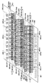
図10は実施例3に従う素子基板を示す図である。図10から明らかなように、素子基板301の形状は平行四辺形であり、その形状に合わせて内部の記録素子、配線、トランジスタが配置されている。この実施例の駆動回路の構成は実施例2で説明した図9に示される構成と同じである。図10を実施例1で説明した図8に示す構成と比較すると素子基板の形状の変化に伴って、各構成要素や配線のレイアウトが異なっているが、各構成要素や配線そのものは同じである。従って、図10では構成要素や配線そのものについての説明は省略し、その参照番号のみを実施例2では2xx又は2xx−yyyと記載していたのを実施例3では3xx又は3xx−yyyと記載して、その構成要素が実施例3に係るものであることを示す。
FIG. 10 is a view showing an element substrate according to the third embodiment. As is apparent from FIG. 10, the
実施例3では実施例2と同様に電源配線306とグランド配線307は素子基板301内の全ての記録要素に接続するように、記録素子302−hijとインク供給口303−hijの間を格子状に接続されている。これにより、例えば、グループ309−1の記録素子302−h1jは配線を流れる電流が分散されるため、実施例2と同様に配線抵抗による電圧降下の差はない。一方、グループ309−mの記録素子302−hmjは素子基板301の形状から電流経路が限られるため、電流が分散されず他のグループに比べて配線抵抗が高くなってしまう。
In the third embodiment, as in the second embodiment, the
そのため、この実施例では、同じ記録素子列内でもグループ309−mではトランジスタの面積を変更する。例えば、記録素子302−kmnを駆動するトランジスタ308−kmnはk列の他のトランジスタ308−k11〜308−km(n−1)よりもその面積を大きく形成する。これにより、電源配線及びグランド配線抵抗にグループ309−mの記録素子で差があったとしても記録素子に印加される電圧を一定にすることができる。 Therefore, in this embodiment, the area of the transistor is changed in the group 309-m even in the same printing element array. For example, the transistor 308-kmn for driving the printing element 302-kmn is formed to have a larger area than the other transistors 308-k11 to 308-km (n-1) in the k columns. Thereby, even if there is a difference between the power supply wiring and the ground wiring resistance among the recording elements of the group 309-m, the voltage applied to the recording elements can be made constant.
図10に示されるように、この実施例では記録素子列の方向とグループ分割の方向とにトランジスタのサイズを変化させている。具体的には、記録素子列の方向に関し、第k列の第1番目(11)のトランジスタのサイズをHk1、第m×n番目(mn)のトランジスタのサイズをHkmとすれば、Hk1<Hkmである。また、第2列の第1番目(11)トランジスタのサイズをH21、第m×n番目(mn)のトランジスタのサイズをH2mとすれば、H21<H2mである。同様に、第1列の第1番目(11)のトランジスタのサイズをH11、第m×n番目(mn)のトランジスタのサイズをH1mとすれば、H11<H1mである。ここで、Hkm>……>H2m>H1mであり、Hk1>……>H21>H11である。このように、電極パッドからの距離が遠く、平行四辺形の端部に近づくほどトランジスタのサイズが大きくなる。 As shown in FIG. 10, in this embodiment, the transistor size is changed in the direction of the recording element array and the direction of group division. Specifically, regarding the direction of the printing element array, if the size of the first (11) transistor in the k-th column is Hk1, and the size of the m × n-th (mn) transistor is Hkm, Hk1 <Hkm. It is. If the size of the first (11) transistor in the second column is H21 and the size of the m × n-th (mn) transistor is H2m, then H21 <H2m. Similarly, if the size of the first (11) transistor in the first column is H11 and the size of the m × n-th (mn) transistor is H1m, then H11 <H1m. Here, Hkm> ...> H2m> H1m, and Hk1> ...> H21> H11. Thus, the transistor size increases as the distance from the electrode pad increases and the end of the parallelogram approaches.
さらに電極パッドに近い方の平行四辺形の端部に近い記録素子を駆動するトランジスタのサイズを一層小さくしても良い。例えば、記録素子302−111を駆動するトランジスタ308−111の面積を、第1列の他のトランジスタ308−112〜308−1m(n−1)の面積よりも小さく形成するのである。ただ、電極パッドに近い記録素子は配線抵抗も小さく、電圧降下そのものが小さいので、吐出特性を均一化するための寄与は少ない。 Further, the size of the transistor that drives the recording element near the end of the parallelogram closer to the electrode pad may be further reduced. For example, the area of the transistor 308-111 that drives the recording element 302-111 is formed to be smaller than the areas of the other transistors 308-112 to 308-1m (n-1) in the first column. However, since the recording element close to the electrode pad has a small wiring resistance and a small voltage drop itself, the contribution for making the ejection characteristics uniform is small.
従って以上説明した実施例によれば、記録素子列の方向とグループ分割の方向にトランジスタの面積を変化させることで、素子基板の形状が平行四辺形であったとしても、各記録素子で安定した吐出特性を得ることができる。また、トランジスタの面積を変化させる際に記録素子列の方向に小さくすることで、電極パッドから記録素子への配線長を短くし、配線抵抗値を低減することができ、素子基板のサイズも削減することも可能となる。 Therefore, according to the embodiment described above, by changing the area of the transistor in the direction of the recording element array and the direction of grouping, even if the shape of the element substrate is a parallelogram, each recording element is stable. Discharge characteristics can be obtained. Also, by reducing the area of the transistor in the direction of the recording element row, the wiring length from the electrode pad to the recording element can be shortened, the wiring resistance value can be reduced, and the element substrate size can also be reduced. It is also possible to do.
なお、電極パッドは素子基板の片側だけではなく両側に配列されていても構わない。その場合も電極パッドからの抵抗値に応じてトランジスタの面積を変化させることで、記録素子への印加電圧を一定にすることができる。また、電源配線及びグランド配線は素子基板内で全ての記録素子に接続される構成でなくても良く、例えば、記録素子が複数のグループ309−1〜mに分割され、各グループで格子状に接続されている構成でも良い。 The electrode pads may be arranged not only on one side of the element substrate but also on both sides. Also in that case, the voltage applied to the recording element can be made constant by changing the area of the transistor in accordance with the resistance value from the electrode pad. Further, the power supply wiring and the ground wiring do not have to be connected to all the recording elements in the element substrate. For example, the recording elements are divided into a plurality of groups 309-1 to 309-m, and each group has a lattice shape. A connected configuration may be used.
さらに、素子基板の形状は平行四辺形である必要はなく、台形や六角形など異なる形状でも良い。 Furthermore, the shape of the element substrate does not have to be a parallelogram, and may be a different shape such as a trapezoid or a hexagon.
また、以上説明した3つの実施例では素子基板がインクを吐出して記録を行う記録ヘッドに実装され、その記録ヘッドが記録装置に搭載されるものとして説明した。しかしながら、その素子基板は必ずしも、記録ヘッドそして記録装置に用いられるものでなくても良い。例えば、その素子基板が何らかの薬剤や液体を吐出する液体吐出ヘッドに実装されるものであっても良い。この場合、記録素子はより一般的に電気熱変換素子(ヒータ)と呼ばれるものとなり、記録素子列は電気熱変換素子列(ヒータ列)となる。 In the three embodiments described above, the element substrate is mounted on a recording head that performs recording by discharging ink, and the recording head is mounted on a recording apparatus. However, the element substrate is not necessarily used for the recording head and the recording apparatus. For example, the element substrate may be mounted on a liquid discharge head that discharges some medicine or liquid. In this case, the recording element is more commonly referred to as an electrothermal conversion element (heater), and the recording element array is an electrothermal conversion element array (heater array).
101 素子基板、102 記録素子、103 インク供給口、104 電源パッド、
105 グランドパッド、106 電源配線、107 グランド配線、
108 トランジスタ、109 駆動グループ
101 element substrate, 102 recording element, 103 ink supply port, 104 power supply pad,
105 ground pads, 106 power supply wiring, 107 ground wiring,
108 transistors, 109 drive groups
Claims (13)
前記第1の電極パッドと前記第2の電極パッドとは、前記複数のヒータの配列方向に沿って設けられており、
前記複数のヒータ列の内、前記第1の電極パッド及び前記第2の電極パッドとの間隔が相対的に大きい位置に設けられるヒータ列に含まれる前記複数のヒータを駆動する複数の第1のトランジスタのサイズが、前記第1の電極パッド及び前記第2の電極パッドとの間隔が相対的に小さい位置に設けられるヒータ列に含まれる前記複数のヒータを駆動する複数の第2のトランジスタのサイズより大きく、
前記素子基板は、前記複数のヒータに対応して設けられ、対応する前記複数のヒータに液体を供給するための複数の供給口をさらに備え、
前記第1の配線の少なくとも一部と前記第2の配線の少なくとも一部とは前記複数の供給口の間を通り格子状に形成され、前記複数のヒータに接続されることを特徴とする素子基板。 A plurality of heater rows formed by arranging a plurality of heater rows in parallel; a plurality of transistors corresponding to the plurality of heaters included in the plurality of heater rows; A first electrode pad that supplies a voltage to be applied to the plurality of heaters; a second electrode pad that grounds the plurality of heaters; and a first electrode that connects the first electrode pad and the plurality of heaters. And an element substrate comprising a second wiring connecting the plurality of heaters and the second electrode pad,
The first electrode pad and the second electrode pad are provided along an arrangement direction of the plurality of heaters,
Among the plurality of heater arrays, a plurality of first drives for driving the plurality of heaters included in a heater array provided at a position where the distance between the first electrode pad and the second electrode pad is relatively large. The size of the plurality of second transistors for driving the plurality of heaters included in the heater array provided at a position where the distance between the first electrode pad and the second electrode pad is relatively small. more rather than size,
The element substrate is provided corresponding to the plurality of heaters, and further includes a plurality of supply ports for supplying liquid to the corresponding plurality of heaters,
At least a part of the first wiring and at least a part of the second wiring are formed in a lattice shape passing between the plurality of supply ports, and are connected to the plurality of heaters substrate.
前記第1の電極パッドと前記第2の電極パッドとは、前記複数のヒータの配列方向に沿って設けられており、
前記複数のヒータ列の内、前記第1の電極パッド及び前記第2の電極パッドとの間隔が相対的に大きい位置に設けられるヒータ列に含まれる前記複数のヒータを駆動する複数の第1のトランジスタのサイズが、前記第1の電極パッド及び前記第2の電極パッドとの間隔が相対的に小さい位置に設けられるヒータ列に含まれる前記複数のヒータを駆動する複数の第2のトランジスタのサイズより大きく、
前記複数のヒータ列に含まれる前記複数のヒータはヒータ列ごとに複数のグループに分割され、該分割されたグループに対応して前記第1の電極パッドと前記第1の配線と前記第2の電極パッドと前記第2の配線とがそれぞれ複数、設けられ、
前記複数の第1の配線と前記複数の第2の配線とが前記対応するグループに含まれるヒータに接続されることを特徴とする素子基板。 A plurality of heater rows formed by arranging a plurality of heater rows in parallel; a plurality of transistors corresponding to the plurality of heaters included in the plurality of heater rows; A first electrode pad that supplies a voltage to be applied to the plurality of heaters; a second electrode pad that grounds the plurality of heaters; and a first electrode that connects the first electrode pad and the plurality of heaters. And an element substrate comprising a second wiring connecting the plurality of heaters and the second electrode pad,
The first electrode pad and the second electrode pad are provided along an arrangement direction of the plurality of heaters,
Among the plurality of heater arrays, a plurality of first drives for driving the plurality of heaters included in a heater array provided at a position where the distance between the first electrode pad and the second electrode pad is relatively large. The size of the plurality of second transistors for driving the plurality of heaters included in the heater array provided at a position where the distance between the first electrode pad and the second electrode pad is relatively small. Bigger,
The plurality of heaters included in the plurality of heater arrays are divided into a plurality of groups for each heater array, and the first electrode pad, the first wiring, and the second electrode are associated with the divided groups. A plurality of electrode pads and a plurality of the second wirings are provided,
Element substrate, wherein the plurality of first wirings and the plurality of second wirings are connected to the heater included in the corresponding group.
前記第1の電極パッドと前記第2の電極パッドとは、前記複数のヒータの配列方向に沿って設けられており、
前記複数のヒータ列の内、前記第1の電極パッド及び前記第2の電極パッドとの間隔が相対的に大きい位置に設けられるヒータ列に含まれる前記複数のヒータを駆動する複数の第1のトランジスタのサイズが、前記第1の電極パッド及び前記第2の電極パッドとの間隔が相対的に小さい位置に設けられるヒータ列に含まれる前記複数のヒータを駆動する複数の第2のトランジスタのサイズより大きく、
前記複数のヒータ列それぞれに含まれる複数のヒータが配列される方向に、前記対応する複数のトランジスタのサイズが異なることを特徴とする素子基板。 A plurality of heater rows formed by arranging a plurality of heater rows in parallel; a plurality of transistors corresponding to the plurality of heaters included in the plurality of heater rows; A first electrode pad that supplies a voltage to be applied to the plurality of heaters; a second electrode pad that grounds the plurality of heaters; and a first electrode that connects the first electrode pad and the plurality of heaters. And an element substrate comprising a second wiring connecting the plurality of heaters and the second electrode pad,
The first electrode pad and the second electrode pad are provided along an arrangement direction of the plurality of heaters,
Among the plurality of heater arrays, a plurality of first drives for driving the plurality of heaters included in a heater array provided at a position where the distance between the first electrode pad and the second electrode pad is relatively large. The size of the plurality of second transistors for driving the plurality of heaters included in the heater array provided at a position where the distance between the first electrode pad and the second electrode pad is relatively small. Bigger,
Wherein the direction in which the plurality of heaters are arranged respectively included in the plurality of the heater array, element substrate, characterized in that the size of the corresponding plurality of transistors are different.
前記第1の電極パッドと前記第2の電極パッドとは、前記複数のヒータの配列方向に沿って設けられており、
前記複数のヒータ列の内、前記第1の電極パッド及び前記第2の電極パッドとの間隔が相対的に大きい位置に設けられるヒータ列に含まれる前記複数のヒータを駆動する複数の第1のトランジスタのサイズが、前記第1の電極パッド及び前記第2の電極パッドとの間隔が相対的に小さい位置に設けられるヒータ列に含まれる前記複数のヒータを駆動する複数の第2のトランジスタのサイズより大きく、
前記素子基板の形状は平行四辺形であり、
前記複数の第1のトランジスタのサイズに関し、前記平行四辺形の鋭角部の端部の近くに設けられるトランジスタのサイズは前記鋭角部の端部の近くに設けられないトランジスタのサイズより大きいことを特徴とする素子基板。 A plurality of heater rows formed by arranging a plurality of heater rows in parallel; a plurality of transistors corresponding to the plurality of heaters included in the plurality of heater rows; A first electrode pad that supplies a voltage to be applied to the plurality of heaters; a second electrode pad that grounds the plurality of heaters; and a first electrode that connects the first electrode pad and the plurality of heaters. And an element substrate comprising a second wiring connecting the plurality of heaters and the second electrode pad,
The first electrode pad and the second electrode pad are provided along an arrangement direction of the plurality of heaters,
Among the plurality of heater arrays, a plurality of first drives for driving the plurality of heaters included in a heater array provided at a position where the distance between the first electrode pad and the second electrode pad is relatively large. The size of the plurality of second transistors for driving the plurality of heaters included in the heater array provided at a position where the distance between the first electrode pad and the second electrode pad is relatively small. Bigger,
The shape of the element substrate is a parallelogram,
Regarding the size of the plurality of first transistors, the size of the transistor provided near the end of the acute angle portion of the parallelogram is larger than the size of the transistor not provided near the end of the acute angle portion. element substrate to be.
前記液体吐出ヘッドをインクを吐出して記録を行うインクジェット記録ヘッドとして用いることを特徴とする請求項7に記載の液体吐出ヘッド。 The liquid is ink;
The liquid discharge head according to claim 7 , wherein the liquid discharge head is used as an ink jet recording head that performs recording by discharging ink.
前記複数のヒータ列の内、前記第1の配線における前記第1の電極パッドと前記複数のヒータとの間の電気抵抗と前記第2の配線における前記第2の電極パッドと前記複数のヒータとの間の電気抵抗の合計が相対的に大きいヒータ列に含まれる前記複数のヒータを駆動する複数の第1のトランジスタのサイズが、前記第1の配線における前記第1の電極パッドと前記複数のヒータとの間の電気抵抗と前記第2の配線における前記第2の電極パッドと前記複数のヒータとの間の電気抵抗の合計が相対的に小さいヒータ列に含まれる前記複数のヒータを駆動する複数の第2のトランジスタのサイズより大きく、
前記素子基板は、前記複数のヒータに対応して設けられ、対応する前記複数のヒータに液体を供給するための複数の供給口をさらに備え、
前記第1の配線の少なくとも一部と前記第2の配線の少なくとも一部とは前記複数の供給口の間を通り格子状に形成され、前記複数のヒータに接続されることを特徴とする素子基板。 A plurality of heater rows formed by arranging a plurality of heater rows in parallel; a plurality of transistors corresponding to the plurality of heaters included in the plurality of heater rows; A first electrode pad that supplies a voltage to be applied to the plurality of heaters; a second electrode pad that grounds the plurality of heaters; and a first electrode that connects the first electrode pad and the plurality of heaters. And an element substrate comprising a second wiring connecting the plurality of heaters and the second electrode pad,
Of the plurality of heater rows, the electrical resistance between the first electrode pad and the plurality of heaters in the first wiring, the second electrode pad and the plurality of heaters in the second wiring, The size of the plurality of first transistors for driving the plurality of heaters included in the heater array having a relatively large total electrical resistance between the first electrode pad and the plurality of the plurality of heaters Driving the plurality of heaters included in the heater row in which the sum of the electrical resistance between the heaters and the second electrode pads in the second wiring and the electrical resistances between the plurality of heaters is relatively small. rather larger than the size of the plurality of second transistors,
The element substrate is provided corresponding to the plurality of heaters, and further includes a plurality of supply ports for supplying liquid to the corresponding plurality of heaters,
At least a part of the first wiring and at least a part of the second wiring are formed in a lattice shape passing between the plurality of supply ports, and are connected to the plurality of heaters substrate.
Priority Applications (2)
| Application Number | Priority Date | Filing Date | Title |
|---|---|---|---|
| JP2015001072A JP6470570B2 (en) | 2015-01-06 | 2015-01-06 | Element substrate, liquid discharge head, and recording apparatus |
| US14/982,599 US9604453B2 (en) | 2015-01-06 | 2015-12-29 | Element substrate, liquid discharge head, and printing apparatus |
Applications Claiming Priority (1)
| Application Number | Priority Date | Filing Date | Title |
|---|---|---|---|
| JP2015001072A JP6470570B2 (en) | 2015-01-06 | 2015-01-06 | Element substrate, liquid discharge head, and recording apparatus |
Publications (3)
| Publication Number | Publication Date |
|---|---|
| JP2016124234A JP2016124234A (en) | 2016-07-11 |
| JP2016124234A5 JP2016124234A5 (en) | 2018-02-15 |
| JP6470570B2 true JP6470570B2 (en) | 2019-02-13 |
Family
ID=56286012
Family Applications (1)
| Application Number | Title | Priority Date | Filing Date |
|---|---|---|---|
| JP2015001072A Active JP6470570B2 (en) | 2015-01-06 | 2015-01-06 | Element substrate, liquid discharge head, and recording apparatus |
Country Status (2)
| Country | Link |
|---|---|
| US (1) | US9604453B2 (en) |
| JP (1) | JP6470570B2 (en) |
Families Citing this family (12)
| Publication number | Priority date | Publication date | Assignee | Title |
|---|---|---|---|---|
| JP6882861B2 (en) * | 2016-07-14 | 2021-06-02 | キヤノン株式会社 | Semiconductor devices, liquid discharge heads, liquid discharge head cartridges and recording devices |
| JP6948116B2 (en) * | 2016-07-25 | 2021-10-13 | キヤノン株式会社 | Recording element substrate, recording head, and recording device |
| JP7005232B2 (en) * | 2016-09-27 | 2022-01-21 | キヤノン株式会社 | Recording head, element board, and recording device |
| JP6787111B2 (en) * | 2016-12-22 | 2020-11-18 | セイコーエプソン株式会社 | Liquid discharge device and circuit board |
| JP6827825B2 (en) * | 2017-02-01 | 2021-02-10 | キヤノン株式会社 | Liquid discharge head substrate, liquid discharge head and liquid discharge device |
| JP7109959B2 (en) * | 2017-05-09 | 2022-08-01 | キヤノン株式会社 | Printhead substrate, printhead substrate manufacturing method, semiconductor substrate, semiconductor substrate manufacturing method, and inkjet recording apparatus |
| US10479075B2 (en) * | 2017-05-09 | 2019-11-19 | Canon Kabushiki Kaisha | Print head substrate and method of manufacturing the same, and semiconductor substrate |
| US10603912B2 (en) * | 2017-06-30 | 2020-03-31 | Canon Kabushiki Kaisha | Element board, liquid ejection head, and printing apparatus |
| CA3126057C (en) * | 2019-02-06 | 2023-08-22 | Hewlett-Packard Development Company, L.P. | Die for a printhead |
| ES2885775T3 (en) | 2019-02-06 | 2021-12-15 | Hewlett Packard Development Co | Matrix for a print head |
| AU2019428624B2 (en) | 2019-02-06 | 2022-11-24 | Hewlett-Packard Development Company, L.P. | Die for a printhead |
| JP7162139B2 (en) | 2019-02-06 | 2022-10-27 | ヒューレット-パッカード デベロップメント カンパニー エル.ピー. | die for print head |
Family Cites Families (25)
| Publication number | Priority date | Publication date | Assignee | Title |
|---|---|---|---|---|
| JP3270740B2 (en) * | 1990-01-25 | 2002-04-02 | キヤノン株式会社 | Recording head, substrate for recording head, and ink jet recording apparatus |
| US5144341A (en) * | 1991-04-26 | 1992-09-01 | Xerox Corporation | Thermal ink jet drivers device design/layout |
| JPH07314658A (en) * | 1994-05-25 | 1995-12-05 | Canon Inc | Ink jet recording head |
| JPH1044416A (en) | 1996-07-31 | 1998-02-17 | Canon Inc | Board for ink jet recording head, ink jet head employing it, ink jet head cartridge, and liquid jet unit |
| JP3415499B2 (en) | 1999-07-16 | 2003-06-09 | エヌイーシーマイクロシステム株式会社 | Semiconductor integrated circuit |
| JP3301417B2 (en) * | 1999-09-08 | 2002-07-15 | ソニー株式会社 | Line head controller of printer for printing by thermal action of line head, printer for printing by thermal action of line head, and printing method of printer for printing by thermal action of line head |
| US6412917B1 (en) * | 2001-01-30 | 2002-07-02 | Hewlett-Packard Company | Energy balanced printhead design |
| US6800902B2 (en) * | 2001-02-16 | 2004-10-05 | Canon Kabushiki Kaisha | Semiconductor device, method of manufacturing the same and liquid jet apparatus |
| JP3927902B2 (en) | 2002-11-29 | 2007-06-13 | キヤノン株式会社 | Inkjet recording head, inkjet recording apparatus having the recording head, and substrate for inkjet recording head |
| US20050212857A1 (en) | 2002-11-29 | 2005-09-29 | Canon Kabushiki Kaisha | Recording head and recorder comprising such recording head |
| JP2004243542A (en) | 2003-02-10 | 2004-09-02 | Sony Corp | Liquid discharge device and its manufacturing method |
| US7125105B2 (en) * | 2003-09-08 | 2006-10-24 | Canon Kabushiki Kaisha | Semiconductor device for liquid ejection head, liquid ejection head, and liquid ejection apparatus |
| TWI267446B (en) * | 2003-11-06 | 2006-12-01 | Canon Kk | Printhead substrate, printhead using the substrate, head cartridge including the printhead, method of driving the printhead, and printing apparatus using the printhead |
| JP4449486B2 (en) * | 2004-02-18 | 2010-04-14 | 富士ゼロックス株式会社 | Recording head and image recording apparatus |
| TWI253393B (en) * | 2004-05-27 | 2006-04-21 | Canon Kk | Printhead substrate, printhead, head cartridge, and printing apparatus |
| TWI296573B (en) * | 2005-06-16 | 2008-05-11 | Canon Kk | Element body for recording head and recording head having element body |
| JP2007055071A (en) | 2005-08-24 | 2007-03-08 | Fuji Xerox Co Ltd | Structure and its manufacturing method, and ink droplet discharge device |
| CN101522428B (en) | 2006-10-09 | 2011-10-05 | 西尔弗布鲁克研究股份有限公司 | Printhead ic with open actuator test |
| US7946674B2 (en) * | 2006-10-10 | 2011-05-24 | Silverbrook Research Pty Ltd | Printhead IC with open actuator test |
| US7806495B2 (en) | 2006-12-05 | 2010-10-05 | Canon Kabushiki Kaisha | Head substrate, printhead, head cartridge, and printing apparatus |
| JP5180595B2 (en) | 2008-01-09 | 2013-04-10 | キヤノン株式会社 | Head substrate, recording head, head cartridge, and recording apparatus |
| JP5169599B2 (en) * | 2008-08-04 | 2013-03-27 | セイコーエプソン株式会社 | Liquid ejection device |
| JP2011093237A (en) * | 2009-10-30 | 2011-05-12 | Canon Inc | Substrate for liquid ejection head, liquid ejection head, and liquid ejecting device provided with the head |
| JP5787603B2 (en) * | 2011-04-28 | 2015-09-30 | キヤノン株式会社 | Inkjet recording head and inkjet recording apparatus |
| JP6163016B2 (en) * | 2012-06-20 | 2017-07-12 | キヤノン株式会社 | Printhead substrate, printhead, and printing apparatus |
-
2015
- 2015-01-06 JP JP2015001072A patent/JP6470570B2/en active Active
- 2015-12-29 US US14/982,599 patent/US9604453B2/en active Active
Also Published As
| Publication number | Publication date |
|---|---|
| JP2016124234A (en) | 2016-07-11 |
| US20160193834A1 (en) | 2016-07-07 |
| US9604453B2 (en) | 2017-03-28 |
Similar Documents
| Publication | Publication Date | Title |
|---|---|---|
| JP6470570B2 (en) | Element substrate, liquid discharge head, and recording apparatus | |
| US9597893B2 (en) | Element substrate and liquid discharge head | |
| TWI253393B (en) | Printhead substrate, printhead, head cartridge, and printing apparatus | |
| JP4618789B2 (en) | Inkjet recording apparatus and inkjet recording method | |
| US9688067B2 (en) | Element substrate, printhead, and printing apparatus | |
| US9090065B2 (en) | Ink jet printing apparatus and ink jet printing method | |
| TW200540021A (en) | Printhead substrate, printhead, head cartridge, and printing apparatus | |
| US9358788B2 (en) | Print head die | |
| US20150239242A1 (en) | Print head die | |
| US9278518B2 (en) | Printhead substrate, printhead, and printing apparatus | |
| US11260666B2 (en) | Liquid ejection head and liquid ejection apparatus | |
| US11565518B2 (en) | Voltage drop compensation for inkjet printhead | |
| US11141975B2 (en) | Multilayer structured element substrate, printhead, and printing apparatus | |
| US8300269B2 (en) | Dot forming element arrays at different resolutions | |
| US9834017B2 (en) | Inkjet printer | |
| JP2014061608A (en) | Ultraviolet lamp and ink curing controller | |
| JP2019166802A (en) | Image recorder | |
| JP2020040311A (en) | Element substrate, recording head and recording device | |
| JP2018015953A (en) | Element substrate, recording head and recording apparatus |
Legal Events
| Date | Code | Title | Description |
|---|---|---|---|
| A521 | Written amendment |
Free format text: JAPANESE INTERMEDIATE CODE: A523 Effective date: 20171218 |
|
| A621 | Written request for application examination |
Free format text: JAPANESE INTERMEDIATE CODE: A621 Effective date: 20171218 |
|
| A977 | Report on retrieval |
Free format text: JAPANESE INTERMEDIATE CODE: A971007 Effective date: 20180926 |
|
| A131 | Notification of reasons for refusal |
Free format text: JAPANESE INTERMEDIATE CODE: A131 Effective date: 20181019 |
|
| A521 | Written amendment |
Free format text: JAPANESE INTERMEDIATE CODE: A523 Effective date: 20181211 |
|
| TRDD | Decision of grant or rejection written | ||
| A01 | Written decision to grant a patent or to grant a registration (utility model) |
Free format text: JAPANESE INTERMEDIATE CODE: A01 Effective date: 20181221 |
|
| A61 | First payment of annual fees (during grant procedure) |
Free format text: JAPANESE INTERMEDIATE CODE: A61 Effective date: 20190118 |
|
| R151 | Written notification of patent or utility model registration |
Ref document number: 6470570 Country of ref document: JP Free format text: JAPANESE INTERMEDIATE CODE: R151 |