JP2006140238A - 基板処理装置用部品及びその製造方法 - Google Patents
基板処理装置用部品及びその製造方法 Download PDFInfo
- Publication number
- JP2006140238A JP2006140238A JP2004327077A JP2004327077A JP2006140238A JP 2006140238 A JP2006140238 A JP 2006140238A JP 2004327077 A JP2004327077 A JP 2004327077A JP 2004327077 A JP2004327077 A JP 2004327077A JP 2006140238 A JP2006140238 A JP 2006140238A
- Authority
- JP
- Japan
- Prior art keywords
- processing apparatus
- substrate processing
- component
- focus ring
- silicon carbide
- Prior art date
- Legal status (The legal status is an assumption and is not a legal conclusion. Google has not performed a legal analysis and makes no representation as to the accuracy of the status listed.)
- Pending
Links
Images


Classifications
-
- H—ELECTRICITY
- H01—ELECTRIC ELEMENTS
- H01J—ELECTRIC DISCHARGE TUBES OR DISCHARGE LAMPS
- H01J37/00—Discharge tubes with provision for introducing objects or material to be exposed to the discharge, e.g. for the purpose of examination or processing thereof
- H01J37/32—Gas-filled discharge tubes
- H01J37/32431—Constructional details of the reactor
- H01J37/32623—Mechanical discharge control means
- H01J37/32642—Focus rings
-
- C—CHEMISTRY; METALLURGY
- C04—CEMENTS; CONCRETE; ARTIFICIAL STONE; CERAMICS; REFRACTORIES
- C04B—LIME, MAGNESIA; SLAG; CEMENTS; COMPOSITIONS THEREOF, e.g. MORTARS, CONCRETE OR LIKE BUILDING MATERIALS; ARTIFICIAL STONE; CERAMICS; REFRACTORIES; TREATMENT OF NATURAL STONE
- C04B35/00—Shaped ceramic products characterised by their composition; Ceramics compositions; Processing powders of inorganic compounds preparatory to the manufacturing of ceramic products
- C04B35/515—Shaped ceramic products characterised by their composition; Ceramics compositions; Processing powders of inorganic compounds preparatory to the manufacturing of ceramic products based on non-oxide ceramics
- C04B35/56—Shaped ceramic products characterised by their composition; Ceramics compositions; Processing powders of inorganic compounds preparatory to the manufacturing of ceramic products based on non-oxide ceramics based on carbides or oxycarbides
- C04B35/565—Shaped ceramic products characterised by their composition; Ceramics compositions; Processing powders of inorganic compounds preparatory to the manufacturing of ceramic products based on non-oxide ceramics based on carbides or oxycarbides based on silicon carbide
-
- C—CHEMISTRY; METALLURGY
- C04—CEMENTS; CONCRETE; ARTIFICIAL STONE; CERAMICS; REFRACTORIES
- C04B—LIME, MAGNESIA; SLAG; CEMENTS; COMPOSITIONS THEREOF, e.g. MORTARS, CONCRETE OR LIKE BUILDING MATERIALS; ARTIFICIAL STONE; CERAMICS; REFRACTORIES; TREATMENT OF NATURAL STONE
- C04B41/00—After-treatment of mortars, concrete, artificial stone or ceramics; Treatment of natural stone
- C04B41/0054—Plasma-treatment, e.g. with gas-discharge plasma
-
- C—CHEMISTRY; METALLURGY
- C04—CEMENTS; CONCRETE; ARTIFICIAL STONE; CERAMICS; REFRACTORIES
- C04B—LIME, MAGNESIA; SLAG; CEMENTS; COMPOSITIONS THEREOF, e.g. MORTARS, CONCRETE OR LIKE BUILDING MATERIALS; ARTIFICIAL STONE; CERAMICS; REFRACTORIES; TREATMENT OF NATURAL STONE
- C04B41/00—After-treatment of mortars, concrete, artificial stone or ceramics; Treatment of natural stone
- C04B41/009—After-treatment of mortars, concrete, artificial stone or ceramics; Treatment of natural stone characterised by the material treated
-
- C—CHEMISTRY; METALLURGY
- C04—CEMENTS; CONCRETE; ARTIFICIAL STONE; CERAMICS; REFRACTORIES
- C04B—LIME, MAGNESIA; SLAG; CEMENTS; COMPOSITIONS THEREOF, e.g. MORTARS, CONCRETE OR LIKE BUILDING MATERIALS; ARTIFICIAL STONE; CERAMICS; REFRACTORIES; TREATMENT OF NATURAL STONE
- C04B41/00—After-treatment of mortars, concrete, artificial stone or ceramics; Treatment of natural stone
- C04B41/80—After-treatment of mortars, concrete, artificial stone or ceramics; Treatment of natural stone of only ceramics
Abstract
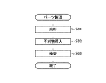
【解決手段】 焼結法又はCVD法によって形成された炭化珪素体を切削加工によってフォーカスリングに成形し(ステップS31)、該成形されたフォーカスリングを、不純物としての四フッ化炭素ガス及び酸素ガスのうち少なくとも1つのガスから生成されたプラズマに晒し、フォーカスリングの表面近傍に存在する空孔状の欠陥に不純物を導入し(ステップS32)、該不純物が導入されたフォーカスリングの表面近傍に陽電子を打ち込み、陽電子消滅法によってフォーカスリングの表面近傍における欠陥存在比を検査する(ステップS33)。
【選択図】 図3
Description
1 エッチング処理装置
2 チャンバ
3 下部電極
4 絶縁材
5 支持体
6 シャワーヘッド
7 上室
8 下室
9 ダイポールリング磁石
10 ゲートバルブ
11 高周波電源
12 整合器
13 静電チャック
14 電極板
15 直流電源
16 フォーカスリング
17 バッフル板
18 排気系
19 ボールねじ
20 ベローズ
21 ベローズカバー
22 プッシャーピン
23 冷媒室
24 配管
25 伝熱ガス供給ライン
26 伝熱ガス供給部
27 バッファ室
28 処理ガス導入管
29 MFC
Claims (7)
- 基板を収容する基板処理装置の収容室内に配置される基板処理装置用部品の製造方法であって、
前記基板処理装置用部品の表面近傍に存在する空孔状の欠陥の存在比を低下させる欠陥存在比低下ステップを有することを特徴とする基板処理装置用部品の製造方法。 - 前記欠陥存在比低下ステップは、前記欠陥に不純物を導入することを特徴とする請求項1記載の基板処理装置用部品の製造方法。
- 前記不純物は、フッ素含有ガス、炭素含有ガス及び酸素含有ガスのうち少なくとも1つのガスから生成されたプラズマから生成されることを特徴とする請求項2記載の基板処理装置用部品の製造方法。
- 前記欠陥存在比低下ステップは、前記基板処理装置用部品を熱処理することを特徴とする請求項1記載の基板処理装置用部品の製造方法。
- 前記欠陥存在比低下ステップは、不活性ガスの雰囲気において前記基板処理装置用部品の温度を1200℃〜1600℃に設定することを特徴とする請求項4記載の基板処理装置用部品の製造方法。
- 前記基板処理装置用部品の表面近傍を陽電子消滅法によって検査する検査ステップを有することを特徴とする請求項1乃至5のいずれか1項に記載の基板処理装置用部品の製造方法。
- 基板を収容する基板処理装置の収容室内に配置される基板処理装置用部品であって、
表面近傍に存在する空孔状の欠陥の存在比が、CVD法によって形成された炭化珪素体の表面近傍に存在する空孔状の欠陥の存在比より低いことを特徴とする基板処理装置用部品。
Priority Applications (6)
| Application Number | Priority Date | Filing Date | Title |
|---|---|---|---|
| JP2004327077A JP2006140238A (ja) | 2004-11-10 | 2004-11-10 | 基板処理装置用部品及びその製造方法 |
| KR1020050105199A KR100735936B1 (ko) | 2004-11-10 | 2005-11-04 | 기판처리장치용 부품 및 그 제조방법 |
| TW094139134A TW200634924A (en) | 2004-11-10 | 2005-11-08 | Components for substrate processing apparatus and manufacturing method thereof |
| US11/270,671 US8058186B2 (en) | 2004-11-10 | 2005-11-10 | Components for substrate processing apparatus and manufacturing method thereof |
| CNB2005101177866A CN100388418C (zh) | 2004-11-10 | 2005-11-10 | 基板处理装置用部件及其制造方法 |
| CN2007101650261A CN101244945B (zh) | 2004-11-10 | 2005-11-10 | 基板处理装置用部件及其制造方法 |
Applications Claiming Priority (1)
| Application Number | Priority Date | Filing Date | Title |
|---|---|---|---|
| JP2004327077A JP2006140238A (ja) | 2004-11-10 | 2004-11-10 | 基板処理装置用部品及びその製造方法 |
Publications (1)
| Publication Number | Publication Date |
|---|---|
| JP2006140238A true JP2006140238A (ja) | 2006-06-01 |
Family
ID=36620872
Family Applications (1)
| Application Number | Title | Priority Date | Filing Date |
|---|---|---|---|
| JP2004327077A Pending JP2006140238A (ja) | 2004-11-10 | 2004-11-10 | 基板処理装置用部品及びその製造方法 |
Country Status (4)
| Country | Link |
|---|---|
| JP (1) | JP2006140238A (ja) |
| KR (1) | KR100735936B1 (ja) |
| CN (2) | CN101244945B (ja) |
| TW (1) | TW200634924A (ja) |
Cited By (3)
| Publication number | Priority date | Publication date | Assignee | Title |
|---|---|---|---|---|
| JP2008211183A (ja) * | 2007-02-27 | 2008-09-11 | Advanced Micro-Fabrication Equipment Inc Asia | 容量的結合型プラズマチェンバー、シャワーヘッドの構造、製造方法並びに新たに再生リサイクルする方法 |
| JP2012049220A (ja) * | 2010-08-25 | 2012-03-08 | Mitsui Eng & Shipbuild Co Ltd | 耐プラズマ部材およびその再生方法 |
| JP2017212427A (ja) * | 2016-05-25 | 2017-11-30 | 韓國東海炭素株式會社 | 半導体製造用部品の再生方法、その再生装置及び再生部品 |
Families Citing this family (4)
| Publication number | Priority date | Publication date | Assignee | Title |
|---|---|---|---|---|
| CN101357854B (zh) * | 2008-09-12 | 2012-07-25 | 西安交通大学 | 一种降低陶瓷热障涂层热导率的后处理方法 |
| CN101748385B (zh) * | 2008-12-22 | 2012-05-09 | 深超光电(深圳)有限公司 | 用于化学气相沉积(cvd)的基板处理设备 |
| JP5415853B2 (ja) * | 2009-07-10 | 2014-02-12 | 東京エレクトロン株式会社 | 表面処理方法 |
| JP6812264B2 (ja) * | 2017-02-16 | 2021-01-13 | 東京エレクトロン株式会社 | 真空処理装置、及びメンテナンス装置 |
Family Cites Families (9)
| Publication number | Priority date | Publication date | Assignee | Title |
|---|---|---|---|---|
| JPH07211700A (ja) * | 1994-01-24 | 1995-08-11 | Sumitomo Metal Ind Ltd | プラズマ発生装置用電極及びその製造方法 |
| KR0170907B1 (ko) * | 1995-10-25 | 1999-03-30 | 김주용 | 반도체 소자의 무결함층 제조방법 |
| KR100203129B1 (ko) | 1995-12-15 | 1999-06-15 | 김영환 | 소오스/드레인 접합 잔류 결함 제거방법 |
| JP3551867B2 (ja) * | 1999-11-09 | 2004-08-11 | 信越化学工業株式会社 | シリコンフォーカスリング及びその製造方法 |
| US6890861B1 (en) * | 2000-06-30 | 2005-05-10 | Lam Research Corporation | Semiconductor processing equipment having improved particle performance |
| WO2003079404A2 (en) * | 2002-03-12 | 2003-09-25 | Tokyo Electron Limited | An improved substrate holder for plasma processing |
| US20030198749A1 (en) * | 2002-04-17 | 2003-10-23 | Applied Materials, Inc. | Coated silicon carbide cermet used in a plasma reactor |
| TW200416208A (en) * | 2002-11-12 | 2004-09-01 | Bridgestone Corp | Silicon carbide sintered product and method for production the same |
| JP4432317B2 (ja) * | 2002-12-11 | 2010-03-17 | 信越半導体株式会社 | シリコンウエーハの熱処理方法 |
-
2004
- 2004-11-10 JP JP2004327077A patent/JP2006140238A/ja active Pending
-
2005
- 2005-11-04 KR KR1020050105199A patent/KR100735936B1/ko active IP Right Grant
- 2005-11-08 TW TW094139134A patent/TW200634924A/zh not_active IP Right Cessation
- 2005-11-10 CN CN2007101650261A patent/CN101244945B/zh not_active Expired - Fee Related
- 2005-11-10 CN CNB2005101177866A patent/CN100388418C/zh not_active Expired - Fee Related
Cited By (4)
| Publication number | Priority date | Publication date | Assignee | Title |
|---|---|---|---|---|
| JP2008211183A (ja) * | 2007-02-27 | 2008-09-11 | Advanced Micro-Fabrication Equipment Inc Asia | 容量的結合型プラズマチェンバー、シャワーヘッドの構造、製造方法並びに新たに再生リサイクルする方法 |
| JP2012049220A (ja) * | 2010-08-25 | 2012-03-08 | Mitsui Eng & Shipbuild Co Ltd | 耐プラズマ部材およびその再生方法 |
| JP2017212427A (ja) * | 2016-05-25 | 2017-11-30 | 韓國東海炭素株式會社 | 半導体製造用部品の再生方法、その再生装置及び再生部品 |
| US10586687B2 (en) | 2016-05-25 | 2020-03-10 | Tokai Carbon Korea Co., Ltd. | Method and apparatus for reproducing component of semiconductor manufacturing apparatus, and reproduced component |
Also Published As
| Publication number | Publication date |
|---|---|
| CN101244945B (zh) | 2013-05-29 |
| KR20060052455A (ko) | 2006-05-19 |
| CN101244945A (zh) | 2008-08-20 |
| CN1790615A (zh) | 2006-06-21 |
| TW200634924A (en) | 2006-10-01 |
| TWI380360B (ja) | 2012-12-21 |
| KR100735936B1 (ko) | 2007-07-06 |
| CN100388418C (zh) | 2008-05-14 |
Similar Documents
| Publication | Publication Date | Title |
|---|---|---|
| US8058186B2 (en) | Components for substrate processing apparatus and manufacturing method thereof | |
| US6767844B2 (en) | Plasma chamber equipped with temperature-controlled focus ring and method of operating | |
| JP6812224B2 (ja) | 基板処理装置及び載置台 | |
| US9922824B2 (en) | Method of forming silicon film | |
| US9735021B2 (en) | Etching method | |
| US9496147B2 (en) | Plasma processing apparatus and plasma processing method | |
| KR102455673B1 (ko) | 포커스 링 및 기판 처리 장치 | |
| KR100735936B1 (ko) | 기판처리장치용 부품 및 그 제조방법 | |
| KR20160140420A (ko) | 플라즈마 처리 장치 및 기판 박리 검지 방법 | |
| TW201729235A (zh) | 藉由光學診斷之電漿不穩定性的偵測系統及方法 | |
| KR20100133910A (ko) | 플라즈마 처리장치용의 소모품의 재이용 방법 | |
| JP2009245988A (ja) | プラズマ処理装置、チャンバ内部品及びチャンバ内部品の寿命検出方法 | |
| KR20120111992A (ko) | 기판 처리 장치, 반도체 장치의 제조 방법, 기판 처리 방법 및 서셉터 커버 | |
| KR20160023646A (ko) | Icp 플라즈마 프로세싱 챔버에서의 기판 최외곽 엣지 결함 감소, 높은 수율을 위한 단일 링 디자인 | |
| JP2016530705A (ja) | 縁部クリティカルディメンジョンの均一性制御用のプロセスキット | |
| JPWO2008041702A1 (ja) | プラズマドーピング方法及び装置 | |
| US20150200081A1 (en) | Method for manufacturing semiconductor device, substrate processing apparatus and non-transitory computer-readable recording medium | |
| US20100263196A1 (en) | Substrate processing apparatus, substrate processing method, and storage medium storing program for implementing the method | |
| JP2006216602A (ja) | 基板処理装置及び基板処理方法 | |
| US8268721B2 (en) | Semiconductor device and semiconductor device manufacturing method | |
| JP2011049567A (ja) | 分割可能な電極及びこの電極を用いたプラズマ処理装置ならびに電極交換方法 | |
| KR101124795B1 (ko) | 플라즈마 처리장치, 챔버내 부품 및 챔버내 부품의 수명 검출 방법 | |
| TWI775987B (zh) | 電漿處理裝置 | |
| KR101224529B1 (ko) | 열처리장치 | |
| US20180190500A1 (en) | Method for etching multilayer film |
Legal Events
| Date | Code | Title | Description |
|---|---|---|---|
| RD03 | Notification of appointment of power of attorney |
Free format text: JAPANESE INTERMEDIATE CODE: A7423 Effective date: 20060427 |
|
| A621 | Written request for application examination |
Free format text: JAPANESE INTERMEDIATE CODE: A621 Effective date: 20071101 |
|
| A977 | Report on retrieval |
Free format text: JAPANESE INTERMEDIATE CODE: A971007 Effective date: 20090624 |
|
| A131 | Notification of reasons for refusal |
Free format text: JAPANESE INTERMEDIATE CODE: A131 Effective date: 20090707 |
|
| A02 | Decision of refusal |
Free format text: JAPANESE INTERMEDIATE CODE: A02 Effective date: 20100209 |