JP2006099500A - Regulator circuit - Google Patents
Regulator circuit Download PDFInfo
- Publication number
- JP2006099500A JP2006099500A JP2004285807A JP2004285807A JP2006099500A JP 2006099500 A JP2006099500 A JP 2006099500A JP 2004285807 A JP2004285807 A JP 2004285807A JP 2004285807 A JP2004285807 A JP 2004285807A JP 2006099500 A JP2006099500 A JP 2006099500A
- Authority
- JP
- Japan
- Prior art keywords
- transistor
- output
- terminal
- regulator circuit
- circuit
- Prior art date
- Legal status (The legal status is an assumption and is not a legal conclusion. Google has not performed a legal analysis and makes no representation as to the accuracy of the status listed.)
- Pending
Links
Images


Classifications
-
- H—ELECTRICITY
- H01—ELECTRIC ELEMENTS
- H01Q—ANTENNAS, i.e. RADIO AERIALS
- H01Q1/00—Details of, or arrangements associated with, antennas
- H01Q1/12—Supports; Mounting means
- H01Q1/22—Supports; Mounting means by structural association with other equipment or articles
- H01Q1/24—Supports; Mounting means by structural association with other equipment or articles with receiving set
- H01Q1/241—Supports; Mounting means by structural association with other equipment or articles with receiving set used in mobile communications, e.g. GSM
- H01Q1/242—Supports; Mounting means by structural association with other equipment or articles with receiving set used in mobile communications, e.g. GSM specially adapted for hand-held use
-
- H—ELECTRICITY
- H01—ELECTRIC ELEMENTS
- H01Q—ANTENNAS, i.e. RADIO AERIALS
- H01Q1/00—Details of, or arrangements associated with, antennas
- H01Q1/08—Means for collapsing antennas or parts thereof
- H01Q1/10—Telescopic elements
-
- H—ELECTRICITY
- H01—ELECTRIC ELEMENTS
- H01Q—ANTENNAS, i.e. RADIO AERIALS
- H01Q11/00—Electrically-long antennas having dimensions more than twice the shortest operating wavelength and consisting of conductive active radiating elements
- H01Q11/02—Non-resonant antennas, e.g. travelling-wave antenna
- H01Q11/08—Helical antennas
Abstract
Description
本発明は、レギュレータ回路に関し、特に、大電流出力を必要とするシリーズレギュレータICに関する。 The present invention relates to a regulator circuit, and more particularly to a series regulator IC that requires a large current output.
レギュレータ回路は、外部から供給される電源電圧を安定化し、安定化された出力電圧を出力端子へ供給する回路である。レギュレータ回路の出力端子には、出力コンデンサ(出力容量)が接続された上で、負荷が接続される。これにより、負荷には、レギュレータ回路で安定化され、かつ出力コンデンサで平滑化された出力電圧が供給される。 The regulator circuit is a circuit that stabilizes a power supply voltage supplied from the outside and supplies a stabilized output voltage to an output terminal. An output capacitor (output capacitance) is connected to the output terminal of the regulator circuit, and then a load is connected. Thereby, the output voltage stabilized by the regulator circuit and smoothed by the output capacitor is supplied to the load.
レギュレータ回路の出力側に接続される出力コンデンサCOとしては、電解コンデンサやタンタルコンデンサが一般的であるが、小型化の要請などに応えるため、より小容量のセラミックコンデンサも用いられるようになってきている。 As the output capacitor CO connected to the output side of the regulator circuit, an electrolytic capacitor or a tantalum capacitor is generally used. However, in order to meet a demand for downsizing, a smaller-capacitance ceramic capacitor is also used. ing.
ところで、コンデンサは、その種類によって異なるESR値(Equivalent Series Resistance:等価直列抵抗)を持つことが知られている。例えば、電解コンデンサは、周波数や温度により変化するが、おおよそ0.1〜100[Ω]のESR値を有し、タンタルコンデンサは、0.01〜1[Ω]のESR値を有する。また、セラミックコンデンサは、0.001〜0.1[Ω]のESR値を有している。そして、レギュレータ回路の出力端子に接続される出力コンデンサのESR値が、レギュレータ回路の位相補償レンジとの関係において適切でない場合、発振が生じることがある。 Incidentally, it is known that a capacitor has an ESR value (Equivalent Series Resistance) that varies depending on the type of the capacitor. For example, although an electrolytic capacitor changes with frequency and temperature, it has an ESR value of approximately 0.1 to 100 [Ω], and a tantalum capacitor has an ESR value of 0.01 to 1 [Ω]. The ceramic capacitor has an ESR value of 0.001 to 0.1 [Ω]. If the ESR value of the output capacitor connected to the output terminal of the regulator circuit is not appropriate in relation to the phase compensation range of the regulator circuit, oscillation may occur.
従来のレギュレータ回路は、例えば、図1に示されるように構成されている。 A conventional regulator circuit is configured, for example, as shown in FIG.
図示のレギュレータ回路は、電源端子VDDと、接地端子GNDと、出力端子VOUTとを有する3端子レギュレータ回路(シリーズレギュレータIC)である。図示のレギュレータ回路は、出力電流が例えば150mA以上の大電流出力用であるので、それを構成するトランジスタはバイポーラトランジスタである。周知のように、バイポーラトランジスタは、制御端子としてベースを持ち、一対の主要電極端子としてコレクタおよびエミッタを持つ。 The illustrated regulator circuit is a three-terminal regulator circuit (series regulator IC) having a power supply terminal V DD , a ground terminal GND, and an output terminal VOUT . The regulator circuit shown is for a large current output with an output current of, for example, 150 mA or more. Therefore, the transistor constituting the regulator circuit is a bipolar transistor. As is well known, a bipolar transistor has a base as a control terminal and a collector and an emitter as a pair of main electrode terminals.
このレギュレータ回路は、定電流源11と、第1乃至第10のトランジスタQ1〜Q10と、第1及び第2の抵抗器R1、R2と、位相補正用コンデンサC1とを有している。
This regulator circuit includes a constant
定電流源11と第1乃至第8のトランジスタQ1〜Q8とは、第1及び第2の抵抗器R1、R2で分圧された分圧電圧と、図示しない参照電圧生成回路で生成された参照電圧との差に応じた誤差信号を発生するエラーアンプを構成する。
The constant
第9のトランジスタQ9は、エラーアンプが出力する誤差信号を増幅して第10のトランジスタQ10のベースに供給する制御トランジスタとして働く。 The ninth transistor Q9 functions as a control transistor that amplifies the error signal output from the error amplifier and supplies it to the base of the tenth transistor Q10.
第10のトランジスタQ10は、電源端子VDDと出力端子VOUTとの間に接続される出力トランジスタ(パワートランジスタ)であって、電源端子VDDに与えられる入力電圧をレギュレートして出力電圧を出力端子VOUTへ供給する。 The tenth transistor Q10 is an output transistor (power transistor) connected between the power supply terminal V DD and the output terminal VOUT, and regulates the input voltage applied to the power supply terminal V DD to generate an output voltage. Supply to the output terminal VOUT .
第1及び第2の抵抗器R1及びR2は、互いに直列接続され、出力端子VOUTと接地端子GNDとの間に接続される。これら抵抗器R1及びR2は、前述の通り、出力電圧を分圧して分圧電圧を生成する分圧回路として働く。 The first and second resistors R1 and R2 are connected in series with each other and connected between the output terminal VOUT and the ground terminal GND. As described above, the resistors R1 and R2 function as a voltage dividing circuit that divides the output voltage to generate a divided voltage.
位相補正用コンデンサC1は、出力端子VOUTと上記分圧回路の分圧電圧を生成する中間ノードN1との間に接続されている。 The phase correcting capacitor C1 is connected between the output terminal VOUT and the intermediate node N1 that generates the divided voltage of the voltage dividing circuit.
第1及び第2の抵抗器R1及びR2と位相補正用コンデンサC1との組み合わせは、進相補償回路として動作する(例えば、非特許文献1参照)。また、上述したレギュレータ回路は、例えば非特許文献2に記載されている。 The combination of the first and second resistors R1 and R2 and the phase correcting capacitor C1 operates as a phase advance compensation circuit (see, for example, Non-Patent Document 1). Moreover, the regulator circuit mentioned above is described in the nonpatent literature 2, for example.
次に、エラーアンプの構成について説明する。第1のトランジスタQ1は、npn形バイポーラトランジスタから成り、そのベースには基準電圧が供給される。第2のトランジスタQ2も、npn形バイポーラトランジスタから成り、そのベースには分圧電圧が供給される。第1のトランジスタQ1と第2のトランジスタQ2のエミッタ同士は接続され、定電流源11を介して接地される。
Next, the configuration of the error amplifier will be described. The first transistor Q1 is formed of an npn bipolar transistor, and a reference voltage is supplied to its base. The second transistor Q2 is also composed of an npn bipolar transistor, and a divided voltage is supplied to its base. The emitters of the first transistor Q1 and the second transistor Q2 are connected to each other and grounded via the constant
第1のトランジスタQ1のコレクタと電源端子VDDとの間には、第3および第4のトランジスタQ3、Q4から構成される第1のカレントミラー回路が接続されている。第3および第4のトランジスタQ3、Q4は、pnp形バイポーラトランジスタから成る。第3および第4のトランジスタQ3、Q4のエミッタは電源端子VDDに接続されている。第3のトランジスタQ3のベースは第4のトランジスタQ4のベースに接続されている。第4のトランジスタQ4のベースは、第4のトランジスタQ4のコレクタに接続されている。第4のトランジスタQ4のコレクタは第1のトランジスタQ1のコレクタに接続されている。 A first current mirror circuit composed of third and fourth transistors Q3 and Q4 is connected between the collector of the first transistor Q1 and the power supply terminal VDD . The third and fourth transistors Q3 and Q4 are pnp bipolar transistors. The emitters of the third and fourth transistors Q3 and Q4 are connected to the power supply terminal VDD . The base of the third transistor Q3 is connected to the base of the fourth transistor Q4. The base of the fourth transistor Q4 is connected to the collector of the fourth transistor Q4. The collector of the fourth transistor Q4 is connected to the collector of the first transistor Q1.
第2のトランジスタQ2のコレクタと電源端子VDDとの間には、第5および第6のトランジスタQ5、Q6から構成される第2のカレントミラー回路が接続されている。第5および第6のトランジスタQ5、Q6は、pnp形バイポーラトランジスタから成る。第5および第6のトランジスタQ5、Q6のエミッタは電源端子VDDに接続されている。第5のトランジスタQ5のベースは第6のトランジスタQ6のベースに接続されている。第6のトランジスタQ6のベースは、第6のトランジスタQ6のコレクタに接続されている。第6のトランジスタQ6のコレクタは第2のトランジスタQ2のコレクタに接続されている。 A second current mirror circuit composed of fifth and sixth transistors Q5 and Q6 is connected between the collector of the second transistor Q2 and the power supply terminal VDD . The fifth and sixth transistors Q5 and Q6 are pnp bipolar transistors. The emitters of the fifth and sixth transistors Q5 and Q6 are connected to the power supply terminal VDD . The base of the fifth transistor Q5 is connected to the base of the sixth transistor Q6. The base of the sixth transistor Q6 is connected to the collector of the sixth transistor Q6. The collector of the sixth transistor Q6 is connected to the collector of the second transistor Q2.
第1のカレントミラー回路および第2のカレントミラー回路と接地端子との間には、第7および第8のトランジスタQ7、Q8から構成される第3のカレントミラー回路が接続されている。第7および第8のトランジスタQ7、Q8は、npn形バイポーラトランジスタから成る。第7および第8のトランジスタQ7、Q8のエミッタは接地端子に接続されている。第7のトランジスタQ7のベースは第8のトランジスタQ8のベースに接続されている。第7のトランジスタQ7のコレクタは第3のトランジスタQ3のコレクタに接続されている。第8のトランジスタQ8のベースは第8のトランジスタQ8のコレクタに接続されている。第8のトランジスタQ8のコレクタは第5のトランジスタQ5のコレクタに接続されている。 A third current mirror circuit composed of seventh and eighth transistors Q7 and Q8 is connected between the first current mirror circuit and the second current mirror circuit and the ground terminal. The seventh and eighth transistors Q7 and Q8 are npn-type bipolar transistors. The emitters of the seventh and eighth transistors Q7 and Q8 are connected to the ground terminal. The base of the seventh transistor Q7 is connected to the base of the eighth transistor Q8. The collector of the seventh transistor Q7 is connected to the collector of the third transistor Q3. The base of the eighth transistor Q8 is connected to the collector of the eighth transistor Q8. The collector of the eighth transistor Q8 is connected to the collector of the fifth transistor Q5.
第1のカレントミラー回路と第3のカレントミラー回路との接続点(換言すれば、第3のトランジスタQ3および第7のトランジスタQ7のコレクタ)が、上記誤差信号を出力する出力ノードである。 A connection point between the first current mirror circuit and the third current mirror circuit (in other words, the collectors of the third transistor Q3 and the seventh transistor Q7) is an output node that outputs the error signal.
制御トランジスタとして動作する第9のトランジスタQ9は、npn形バイポーラトランジスタから成り、そのベースが上記出力ノードに接続され、エミッタが接地端子に接続されている。 The ninth transistor Q9 operating as a control transistor is composed of an npn-type bipolar transistor, the base of which is connected to the output node, and the emitter of which is connected to the ground terminal.
出力トランジスタとして動作する第10のトランジスタQ10は、pnp形バイポーラトランジスタから成り、そのベースが第9のトランジスタQ9のコレクタに接続され、エミッタが電源端子VDDに接続され、コレクタが出力端子VOUTに接続されている。 The tenth transistor Q10 operating as an output transistor is composed of a pnp bipolar transistor, the base thereof is connected to the collector of the ninth transistor Q9, the emitter is connected to the power supply terminal V DD , and the collector is connected to the output terminal VOUT . It is connected.
図1のレギュレータ回路において、電源端子VDDに電源電圧(例えば、3〜7[V])が与えられると、第1及び第2のトランジスタQ1,Q2には、これらのベースに与えられる電圧差に応じた電流が流れる。第1のトランジスタQ1のベースに供給される参照電圧は、例えば、0.6〜1.2[V]である。 In the regulator circuit of FIG. 1, when a power supply voltage (for example, 3 to 7 [V]) is applied to the power supply terminal V DD , the voltage difference applied to the bases of the first and second transistors Q1 and Q2 A current corresponding to the current flows. The reference voltage supplied to the base of the first transistor Q1 is, for example, 0.6 to 1.2 [V].
第1及び第2のカレントミラー回路は、第1及び第2のトランジスタQ1,Q2に流れる電流と同じ大きさの電流を第7及び第8のトランジスタQ7,Q8にそれぞれ流す。第7及び第8のトランジスタQ7,Q8に供給される電流の差が、第9のトランジスタQ9のベースに電圧(誤差信号)を与え、それによって第9のトランジスタQ9に流れる電流が変化する。その結果、第10のトランジスタQ10のベース電流が変化し、出力端子VOUTに供給される出力電圧(例えば、0.8〜5[V])がレギュレート(安定化)される。 The first and second current mirror circuits pass currents of the same magnitude as the currents flowing through the first and second transistors Q1 and Q2 to the seventh and eighth transistors Q7 and Q8, respectively. The difference between the currents supplied to the seventh and eighth transistors Q7 and Q8 gives a voltage (error signal) to the base of the ninth transistor Q9, whereby the current flowing through the ninth transistor Q9 changes. As a result, the base current of the tenth transistor Q10 changes, and the output voltage (for example, 0.8 to 5 [V]) supplied to the output terminal VOUT is regulated (stabilized).
位相補正用コンデンサC1は、例えば、20pFの容量値を持ち、このレギュレータ回路の位相補償レンジを拡大(位相進み補償)する。 The phase correction capacitor C1 has, for example, a capacitance value of 20 pF, and expands the phase compensation range of this regulator circuit (phase advance compensation).
一般に、レギュレータ回路が発振しないためには、ゲインが0dBになる周波数での位相余裕(マージン)が例えば45°以上に保たれている必要がある。 In general, in order for the regulator circuit not to oscillate, the phase margin (margin) at a frequency where the gain becomes 0 dB needs to be maintained at 45 ° or more, for example.
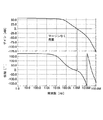
図2に、図1のレギュレータ回路から位相補正用コンデンサC1を削除したレギュレータ回路において、出力コンデンサCOのESRが0.01Ω、出力電流が500mAのときの、レギュレータ回路のオープンループ特性を示す。この図2から、位相補正用コンデンサC1がないレギュレータ回路では、ゲインが0dBになる周波数での位相余裕(マージン)がないことが分かる。そのため、位相補正用コンデンサC1がないレギュレータ回路は発振する。 Figure 2 illustrates the regulator circuit which removes the phase correction capacitor C1 from the regulator circuit of FIG. 1, the output capacitor C ESR of O is 0.01 Ohm, when the output current is 500mA, the open-loop characteristics of the regulator circuit. From FIG. 2, it can be seen that the regulator circuit without the phase correction capacitor C1 has no phase margin (margin) at a frequency at which the gain becomes 0 dB. Therefore, the regulator circuit without the phase correction capacitor C1 oscillates.
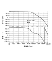
図3に、図1のレギュレータ回路において、出力コンデンサCOのESRが0.01Ω、出力電流が500mAのときの、レギュレータ回路のオープンループ特性を示す。この図3から、位相補正用コンデンサC1があるレギュレータ回路でも、ゲインが0dBになる周波数での位相余裕(マージン)がないことが分かる。そのため、位相補正用コンデンサC1があるレギュレータ回路でも発振する。 3 shows the regulator circuit of FIG. 1, the output capacitor C ESR of O is 0.01 Ohm, when the output current is 500mA, the open-loop characteristics of the regulator circuit. As can be seen from FIG. 3, even in the regulator circuit having the phase correction capacitor C1, there is no phase margin (margin) at a frequency at which the gain becomes 0 dB. Therefore, even the regulator circuit having the phase correction capacitor C1 oscillates.
このように、出力コンデンサCOのESRが低い場合には、たとえ位相補正用コンデンサC1を設けたとしても、レギュレータ回路が発振することが分かる。 Thus, it can be seen that when the ESR of the output capacitor CO is low, the regulator circuit oscillates even if the phase correction capacitor C1 is provided.
上述したように、従来のレギュレータ回路は、出力コンデンサCOの低容量化、低ESR化に対応することが困難であるという問題点を有している。 As described above, the conventional regulator circuit has a problem that it is difficult to cope with the reduction in the capacitance and the ESR of the output capacitor CO .
そこで、本発明は、出力コンデンサCOの低容量化、低ESR化に対応できるレギュレータ回路を提供することを目的とする。 Therefore, an object of the present invention is to provide a regulator circuit that can cope with a reduction in the capacitance and ESR of the output capacitor CO .
本発明によれば、電源端子(VDD)と出力端子(VOUT)と接地端子とを持つレギュレータ回路であって、前記電源端子と前記出力端子との間に接続された出力トランジスタ(Q10)と、該出力端子と前記接地端子との間の出力電圧を分圧して中間ノード(N1)から分圧電圧を生成する分圧回路(R1,R2)と、基準電圧と前記分圧電圧との差に応じた誤差信号を発生するエラーアンプ(Q1〜Q8、11)と、前記誤差信号に応じて前記出力トランジスタを制御する制御トランジスタ(Q9)とを備え、前記出力トランジスタを制御することにより前記出力電圧を安定化させる、前記レギュレータ回路において、前記出力端子と前記分圧回路の前記中間ノードとの間に接続された第1の位相補正用コンデンサ(C1)と、前記出力端子と前記エラーアンプの所定のノード(N2)との間に接続された第2の位相補正用コンデンサ(C2)とを有することを特徴とするレギュレータ回路が得られる。 According to the present invention, a regulator circuit having a power supply terminal (V DD ), an output terminal (V OUT ), and a ground terminal, the output transistor (Q10) connected between the power supply terminal and the output terminal. A voltage dividing circuit (R1, R2) that divides an output voltage between the output terminal and the ground terminal to generate a divided voltage from the intermediate node (N1), and a reference voltage and the divided voltage An error amplifier (Q1 to Q8, 11) for generating an error signal corresponding to the difference; and a control transistor (Q9) for controlling the output transistor according to the error signal, and controlling the output transistor to control the output transistor. In the regulator circuit for stabilizing an output voltage, a first phase correcting capacitor (C1) connected between the output terminal and the intermediate node of the voltage dividing circuit; A regulator circuit having a second phase correcting capacitor (C2) connected between the output terminal and a predetermined node (N2) of the error amplifier is obtained.
上記レギュレータ回路において、前記エラーアンプは、前記基準電圧が供給される制御端子を持つ第1のトランジスタ(Q1)と、前記分圧電圧が供給される制御端子を持つ第2のトランジスタ(Q2)と、前記第1のトランジスタおよび前記第2のトランジスタの一方の主要電極端子と前記接地端子との間に接続された定電流源(11)と、前記第1のトランジスタの他方の主要電極端子と前記電源端子との間に接続された第1のカレントミラー回路(Q3,Q4)と、前記第2のトランジスタの他方の主要電極端子と前記電源端子との間に接続された第2のカレントミラー回路(Q5,Q6)と、前記第1のカレントミラー回路および前記第2のカレントミラー回路と前記接地端子との間に接続された第3のカレントミラー回路(Q7,Q8)とから構成される。前記第1のカレントミラー回路と前記第3のカレントミラー回路との接続点が前記誤差信号を出力する出力ノード(N3)である。前記第3のカレントミラー回路は、前記出力ノードに一方の主要電極端子が接続されたトランジスタ(Q7)を含み、当該トランジスタの制御端子が前記所定のノード(N2)である。 In the regulator circuit, the error amplifier includes a first transistor (Q1) having a control terminal to which the reference voltage is supplied, and a second transistor (Q2) having a control terminal to which the divided voltage is supplied. A constant current source (11) connected between one main electrode terminal of the first transistor and the second transistor and the ground terminal; the other main electrode terminal of the first transistor; A first current mirror circuit (Q3, Q4) connected between the power terminal and a second current mirror circuit connected between the other main electrode terminal of the second transistor and the power terminal. (Q5, Q6) and a third current mirror circuit (Q7, Q6) connected between the first current mirror circuit and the second current mirror circuit and the ground terminal. Composed from the 8). A connection point between the first current mirror circuit and the third current mirror circuit is an output node (N3) that outputs the error signal. The third current mirror circuit includes a transistor (Q7) having one main electrode terminal connected to the output node, and the control terminal of the transistor is the predetermined node (N2).
また、上記レギュレータ回路において、前記エラーアンプを構成するトランジスタは、バイポーラトランジスタで構成されて良い。その場合、前記第3のカレントミラー回路は、前記第2のカレントミラー回路と前記接地端子との間に接続された別のトランジスタ(Q8)を含み、当該別のトランジスタの制御端子と前記所定のノードとの間には同じ抵抗値を持つ2つの抵抗器(R3,R4)が直列に接続され、該2つの抵抗器の接続点と前記別のトランジスタの一方の主要電極端子とが直接接続されていることが望ましい。 In the regulator circuit, the transistor constituting the error amplifier may be a bipolar transistor. In that case, the third current mirror circuit includes another transistor (Q8) connected between the second current mirror circuit and the ground terminal, and the control terminal of the other transistor and the predetermined transistor Two resistors (R3, R4) having the same resistance value are connected in series with the node, and a connection point between the two resistors and one main electrode terminal of the other transistor are directly connected. It is desirable that
更に、上記レギュレータ回路において、前記第2の位相補正用コンデンサ(C2)は、0.5pF〜20pFの範囲の容量値を持ち、前記2つの抵抗器(R3,R4)の各々は、200Ω〜60kΩの範囲の抵抗値を持つことが好ましい。そして、前記2つの抵抗器の抵抗値と前記第2の位相補正用コンデンサの容量値とで規定される時定数は、進み位相補償を施したい周波数によって決められる。 Further, in the regulator circuit, the second phase correcting capacitor (C2) has a capacitance value in a range of 0.5 pF to 20 pF, and each of the two resistors (R3, R4) is 200 Ω to 60 kΩ. It is preferable to have a resistance value in the range. The time constant defined by the resistance values of the two resistors and the capacitance value of the second phase correction capacitor is determined by the frequency at which the advance phase compensation is desired.
なお、上記括弧内の符号は、本願発明の理解を容易にするために付したものであって、何ら本発明を限定するものではない。 In addition, the code | symbol in the said parenthesis is attached | subjected in order to make an understanding of this invention easy, and does not limit this invention at all.
レギュレータ回路の発振を防止するために、第1の位相補正用コンデンサばかりでなく第2の位相補正用コンデンサをも備えているので、低容量、低ESRに対応できるレギュレータ回路を提供することができる。 In order to prevent oscillation of the regulator circuit, since the second phase correction capacitor is provided in addition to the first phase correction capacitor, a regulator circuit that can cope with low capacitance and low ESR can be provided. .
以下、本発明の実施の形態について図面を参照して詳細に説明する。 Hereinafter, embodiments of the present invention will be described in detail with reference to the drawings.
図4に本発明の一実施の形態に係るレギュレータ回路(シリーズレギュレータIC)の回路図を示す。このレギュレータ回路は、従来のレギュレータ回路とほぼ同じ構成を有しており、第2の位相補正用コンデンサC2を含む位相補正回路部40を有している点で異なっている。
FIG. 4 shows a circuit diagram of a regulator circuit (series regulator IC) according to an embodiment of the present invention. This regulator circuit has substantially the same configuration as a conventional regulator circuit, and is different in that it includes a phase
詳述すると、このレギュレータ回路は、定電流源11と、第1乃至第10のトランジスタQ1〜Q10と、第1及び第2の抵抗器R1、R2と、第1の位相補正用コンデンサC1と、位相補正回路部40とを有している。ここで、位相補正回路部40は、第3及び第4の抵抗器R3及びR4(例えば、5[kΩ]及び5[kΩ])と、第2の位相補正用コンデンサC2(例えば、3[pF])とから構成されている。
More specifically, the regulator circuit includes a constant
換言すると、図示のレギュレータ回路は、電源端子VDDと出力端子VOUTとの間に接続された出力トランジスタQ10と、この出力端子VOUTと接地端子との間の出力電圧を分圧して中間ノードN1から分圧電圧を生成する分圧回路(R1,R2)と、基準電圧と分圧電圧との差に応じた誤差信号を発生するエラーアンプ(Q1〜Q8、11)と、誤差信号に応じて出力トランジスタQ10を制御する制御トランジスタQ9とを備える。レギュレータ回路は、出力トランジスタQ10を制御することにより出力電圧を安定化させるものである。そして、図示のレギュレータ回路は、出力端子VOUTと分圧回路(R1,R2)の中間ノードN1との間に接続された第1の位相補正用コンデンサC1と、出力端子VOUTとエラーアンプの所定のノードN2(後述する)との間に接続された第2の位相補正用コンデンサC2を含む位相補正回路部40とを更に備えている。
In other words, the regulator circuit shown in the figure divides the output voltage between the output transistor Q10 connected between the power supply terminal V DD and the output terminal VOUT and the output terminal VOUT and the ground terminal to generate an intermediate node. A voltage dividing circuit (R1, R2) that generates a divided voltage from N1, an error amplifier (Q1 to Q8, 11) that generates an error signal according to a difference between the reference voltage and the divided voltage, and a response to the error signal And a control transistor Q9 for controlling the output transistor Q10. The regulator circuit stabilizes the output voltage by controlling the output transistor Q10. The illustrated regulator circuit includes a first phase correction capacitor C1 connected between the output terminal VOUT and the intermediate node N1 of the voltage dividing circuit (R1, R2), an output terminal VOUT, and an error amplifier. And a phase
図示のレギュレータ回路は、大電流出力を必要とするレギュレータ回路であるので、それを構成するトランジスタはすべてバイポーラトランジスタで構成されている。周知のように、バイポーラトランジスタは、制御端子としてベースを持ち、一対の主要電極端子としてコレクタ及びエミッタを持っている。 Since the regulator circuit shown in the figure is a regulator circuit that requires a large current output, all the transistors constituting the regulator circuit are bipolar transistors. As is well known, a bipolar transistor has a base as a control terminal and a collector and an emitter as a pair of main electrode terminals.
定電流源11と第1乃至第8のトランジスタQ1〜Q8は、2つの入力信号(後述する分圧電圧及び参照電圧)の差に基づく誤差信号を生成するエラーアンプを構成する。
The constant
第1及び第2のトランジスタQ1及びQ2は、ともにnpn形バイポーラトランジスタから成る。これらトランジスタQ1及びQ2のエミッタは定電流源11に共通に接続され、コレクタは後述する第1及び第2のカレントミラー回路に夫々接続されている。また、第1のトランジスタQ1のベースには、図示しない参照電圧生成回路で生成された参照電圧が供給される。第2のトランジスタQ2のベースには、分圧回路(R1,R2)の中間ノードN1から出力される分圧電圧が供給される。そして、第1及び第2のトランジスタQ1及びQ2は、これらのベースに供給される電圧の差に応じて、定電流源11が生成した定電流を分割する。
The first and second transistors Q1 and Q2 are both npn bipolar transistors. The emitters of these transistors Q1 and Q2 are commonly connected to the constant
第3及び第4のトランジスタQ3及びQ4は、ともにpnp形バイポーラトランジスタから成る。これらトランジスタQ3及びQ4のエミッタはともに電源端子VDDに接続され、ベースは互いに接続されるとともに第4のトランジスタQ4のコレクタにも接続されている。また、第3のトランジスタQ3のコレクタは、後述する第7のトランジスタQ7のコレクタに接続されている。これらトランジスタQ3及びQ4は、第1のカレントミラー回路を構成し、第1のトランジスタQ1に流れる電流と同一の電流を第7のトランジスタQ7に供給する。 The third and fourth transistors Q3 and Q4 are both pnp bipolar transistors. The emitters of the transistors Q3 and Q4 are both connected to the power supply terminal VDD , and the bases are connected to each other and to the collector of the fourth transistor Q4. The collector of the third transistor Q3 is connected to the collector of a seventh transistor Q7 described later. These transistors Q3 and Q4 constitute a first current mirror circuit, and supply the same current as the current flowing through the first transistor Q1 to the seventh transistor Q7.
第5及び第6のトランジスタQ5及びQ6は、ともにpnp形バイポーラトランジスタから成る。これらトランジスタQ5及びQ6のエミッタはともに電源端子VDDに接続され、ベースは互いに接続されるとともに第6のトランジスタQ6のコレクタにも接続されている。また、第5のトランジスタQ5のコレクタは、後述する第8のトランジスタQ8のコレクタに接続されている。これらトランジスタQ5及びQ6は、第2のカレントミラー回路を構成し、第2のトランジスタQ2に流れる電流と同一の電流を第8のトランジスタQ8に供給する。 Both the fifth and sixth transistors Q5 and Q6 are pnp bipolar transistors. The emitters of these transistors Q5 and Q6 are both connected to the power supply terminal VDD , and the bases are connected to each other and to the collector of the sixth transistor Q6. The collector of the fifth transistor Q5 is connected to the collector of an eighth transistor Q8 described later. These transistors Q5 and Q6 constitute a second current mirror circuit, and supply the same current as the current flowing through the second transistor Q2 to the eighth transistor Q8.
第7及び第8のトランジスタQ7及びQ8は、ともにnpn形バイポーラトランジスタから成る。第7のトランジスタ(誤差信号生成用トランジスタ)Q7のエミッタは接地端子に接続され、ベースは位相補正回路部40の第3の抵抗器R3の一方の端子に接続されている。第8のトランジスタQ8のエミッタは接地端子に接続され、ベースは位相補正回路部40の第4の抵抗器R4の一方の端子に接続されている。第8のトランジスタQ8のコレクタは、第3及び第4の抵抗器R3,R4の接続点に接続されている。また、第7及び第8のトランジスタQ7及びQ8は、第3のカレントミラー回路を構成し、第7のトランジスタQ7のコレクタである出力ノードN3に、第7のトランジスタQ7と第8のトランジスタQ8とに夫々供給される電流の差に応じた電圧(誤差信号)を発生させる。
The seventh and eighth transistors Q7 and Q8 are both npn bipolar transistors. The emitter of the seventh transistor (error signal generating transistor) Q7 is connected to the ground terminal, and the base is connected to one terminal of the third resistor R3 of the phase
第9のトランジスタQ9は、npn形バイポーラトランジスタから成る。第9のトランジスタQ9のエミッタは接地端子に、コレクタは第10のトランジスタQ10のベースに、ベースは第7のトランジスタQ7のコレクタ(第3のトランジスタQ3のコレクタ)N3に、夫々接続されている。第9のトランジスタQ9は、誤差信号に応じて第10のトランジスタQ10のベースに流れる電流を制御する制御トランジスタとして動作する。 The ninth transistor Q9 is an npn bipolar transistor. The emitter of the ninth transistor Q9 is connected to the ground terminal, the collector is connected to the base of the tenth transistor Q10, and the base is connected to the collector of the seventh transistor Q7 (the collector of the third transistor Q3) N3. The ninth transistor Q9 operates as a control transistor that controls the current flowing through the base of the tenth transistor Q10 according to the error signal.
第10のトランジスタQ10は、pnp形バイポーラトランジスタから成る。第10のトランジスタQ10のエミッタは電源端子VDDに接続され、コレクタは出力端子VOUTに接続されている。第10のトランジスタQ10は、そのベース電流に応じて、電源端子VDDに与えられる電源電圧をレギュレートし、出力電圧として出力端子VOUTへ供給する。 The tenth transistor Q10 is composed of a pnp bipolar transistor. The emitter of the tenth transistor Q10 is connected to the power supply terminal V DD and the collector is connected to the output terminal VOUT . The tenth transistor Q10 regulates the power supply voltage supplied to the power supply terminal V DD according to the base current, and supplies it to the output terminal VOUT as an output voltage.
第1及び第2の抵抗器R1及びR2は、互いに直列接続され、出力端子VOUTと接地端子との間に接続される。また、これら抵抗器R1及びR2の接続点(中間ノード)N1が、前述の通り第2のトランジスタQ2のベースに接続される。第1及び第2の抵抗器R1及びR2は、出力端子VOUTに供給される出力電圧を分圧し、分圧電圧を第2のトランジスタQ1のベースに供給する分圧回路として働く。 The first and second resistors R1 and R2 are connected in series with each other and connected between the output terminal VOUT and the ground terminal. Further, the connection point (intermediate node) N1 of the resistors R1 and R2 is connected to the base of the second transistor Q2 as described above. The first and second resistors R1 and R2 function as a voltage dividing circuit that divides the output voltage supplied to the output terminal VOUT and supplies the divided voltage to the base of the second transistor Q1.
第1の位相補正用コンデンサC1は、出力端子VOUTと分圧回路の中間ノードN1との間に接続されている。 The first phase correcting capacitor C1 is connected between the output terminal VOUT and the intermediate node N1 of the voltage dividing circuit.
位相補正回路部40の第2の位相補正用コンデンサC2の一方の端子は、出力端子VOUTに接続され、他方の端子は、第7のトランジスタQ7のベースに夫々接続されている。すなわち、第7のトランジスタQ7のベースがエラーアンプの所定のノードN2である。第2の位相補正用コンデンサC2は、出力電圧に応じて第7のトランジスタQ7のベース電位を変化させ、エラーアンプから出力される誤差信号を補正する。
One terminal of the second phase correction capacitor C2 of the phase
以上の構成により、図4のレギュレータ回路は、従来と同様に、電源端子VDDに与えられた電源電圧をレギュレートし、レギュレートされた電源電圧を出力電圧として、出力端子VOUTに供給する。 With the above configuration, the regulator circuit of FIG. 4 regulates the power supply voltage supplied to the power supply terminal V DD and supplies the regulated power supply voltage to the output terminal VOUT as the output voltage, as in the conventional case. .
本実施の形態に係るレギュレータ回路は、第1の位相補正用コンデンサC1ばかりでなく、第2の位相補正用コンデンサC2を含む位相補正回路部40をも備えているので、従来のレギュレータ回路よりもより一層進み位相補償を行うことができる。
The regulator circuit according to the present embodiment includes not only the first phase correction capacitor C1 but also the phase
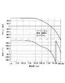
図5に、図4のレギュレータ回路から第3及び第4の抵抗器R3,R4を削除したレギュレータ回路において、出力コンデンサCOのESRが0.01Ω、出力電流が500mAのときの、レギュレータ回路のオープンループ特性を示す。この図5から、第3及び第4の抵抗器R3,R4がないレギュレータ回路では、ゲインが0dBになる周波数での位相余裕(マージン)がないことが分かる。そのため、第3及び第4の抵抗器R3,R4がないレギュレータ回路は発振する。 5, in the regulator circuit deleting the third and fourth resistors R3, R4 from the regulator circuit of FIG. 4, ESR of the output capacitor C O is 0.01 Ohm, the output current when the 500mA, the regulator circuit Shows open loop characteristics. From FIG. 5, it can be seen that the regulator circuit without the third and fourth resistors R3 and R4 has no phase margin (margin) at a frequency at which the gain becomes 0 dB. Therefore, the regulator circuit without the third and fourth resistors R3 and R4 oscillates.
図6に、図4のレギュレータ回路において、出力コンデンサCOのESRが0.01Ω、出力電流が500mAのときの、レギュレータ回路のオープンループ特性を示す。この図6から、図4のレギュレータ回路では、ゲインが0dBになる周波数での位相余裕(マージン)が60°程度あることが分かる。また、位相が0°となる周波数以上の周波数帯では、ゲインが負となっているので、このレギュレータ回路は発振することはない。 Figure 6 shows the regulator circuit of FIG. 4, the output capacitor C ESR of O is 0.01 Ohm, when the output current is 500mA, the open-loop characteristics of the regulator circuit. From FIG. 6, it can be seen that in the regulator circuit of FIG. 4, the phase margin (margin) at a frequency at which the gain becomes 0 dB is about 60 °. Further, since the gain is negative in the frequency band equal to or higher than the frequency at which the phase becomes 0 °, the regulator circuit does not oscillate.
以上説明したように、本実施の形態に係るレギュレート回路は、第1の位相補正用コンデンサC1ばかりでなく、第2の位相補正用コンデンサC2を含む位相補正回路部40をも備えているので、低容量、低ESRの出力コンデンサCOに対応することができる。
As described above, the regulation circuit according to the present embodiment includes not only the first phase correction capacitor C1 but also the phase
尚、位相補正回路部40を構成する第3及び第4の抵抗器R3,R4は、第3のカレントミラー回路を構成する第7及び第8のトランジスタQ7及びQ8のベース−エミッタ間電位を同一にする必要があるので、同じ抵抗値を持っている。また、第3及び第4の抵抗器R3,R4の抵抗値としては、200Ω〜60kΩの範囲であることが望ましい。下限の抵抗値を200Ωと設定したのは、第3及び第4の抵抗器R3,R4を流れる電流が1μA程度で、第7及び第8のトランジスタQ7及びQ8のエミッタ抵抗が26Ω程度あるので、その影響を受けないようにするためである。また、上限の抵抗値を60kΩと設定したのは、それ以上高い抵抗値を製造することは製造プロセス上バラツキが大きくなり、同じ抵抗値を持つ抵抗器を製造することが困難になるからである。
The third and fourth resistors R3 and R4 constituting the phase
一方、第2の位相補正用コンデンサC2の容量値としては、0.5pF〜20pFの範囲にあることが好ましい。上記コンデンサC2の容量値を0.5pF〜20pFの範囲としたのは、上記の容量値を持つコンデンサを半導体上に製造する上での問題より、適度な値としたものである。 On the other hand, the capacitance value of the second phase correcting capacitor C2 is preferably in the range of 0.5 pF to 20 pF. The reason why the capacitance value of the capacitor C2 is set in the range of 0.5 pF to 20 pF is an appropriate value due to a problem in manufacturing a capacitor having the above capacitance value on a semiconductor.
また、第3及び第4の抵抗器R3,R4の抵抗値と第2の位相補正用コンデンサC2の容量値とで規定される時定数は、進み位相補償を施したい周波数によって決められる。 The time constant defined by the resistance values of the third and fourth resistors R3 and R4 and the capacitance value of the second phase correction capacitor C2 is determined by the frequency at which the advance phase compensation is desired.
本発明者は、図4に示すレギュレータ回路において、第7のトランジスタQ7のベース−コレクタ間にコンデンサを接続することにより、さらに進み位相補償の効果が上がることを確認している。そのコンデンサの容量値としては、5pF〜50pFの範囲が適当であった。 The present inventor has confirmed that the effect of the advance phase compensation is further improved by connecting a capacitor between the base and collector of the seventh transistor Q7 in the regulator circuit shown in FIG. As the capacitance value of the capacitor, a range of 5 pF to 50 pF was appropriate.
尚、本発明は、上述した実施の形態に限定されず、本発明の趣旨を逸脱しない範囲で種々の変更が可能なのはいうまでもない。例えば、上述した実施の形態では、バイポーラトランジスタで構成されたレギュレータ回路について説明しているが、本発明は、出力電流が50mA〜100mAの範囲の小出力電流用の場合には、MOSFETで構成されたレギュレータ回路にも同様に適用可能である。各MOSFETは、制御端子としてゲートを持ち、一対の主要電極端子としてドレインおよびソースを持つ。その場合には、第1の位相補正用コンデンサに加えて、少なくとも第2の位相補正用コンデンサを備えたもので構成することができる。 Needless to say, the present invention is not limited to the above-described embodiments, and various modifications can be made without departing from the spirit of the present invention. For example, in the above-described embodiment, a regulator circuit composed of a bipolar transistor is described. However, the present invention is composed of a MOSFET when the output current is for a small output current in the range of 50 mA to 100 mA. The same applies to the regulator circuit. Each MOSFET has a gate as a control terminal and a drain and a source as a pair of main electrode terminals. In that case, in addition to the first phase correction capacitor, at least a second phase correction capacitor may be provided.
11 定電流回路
40 位相補正回路部
Q1〜Q10 トランジスタ
R1〜R4 抵抗器
C1 第1の位相補正用コンデンサ
C2 第2の位相補正用コンデンサ
CO 出力コンデンサ
ESR 等価直列抵抗
VDD 電源端子
VOUT 出力端子
RL 負荷抵抗
11 a constant
Claims (5)
前記出力端子と前記分圧回路の前記中間ノードとの間に接続された第1の位相補正用コンデンサと、
前記出力端子と前記エラーアンプの所定のノードとの間に接続された第2の位相補正用コンデンサと
を有することを特徴とするレギュレータ回路。 A regulator circuit having a power supply terminal, an output terminal, and a ground terminal, wherein an output transistor connected between the power supply terminal and the output terminal and an output voltage between the output terminal and the ground terminal are divided. A voltage dividing circuit that generates a divided voltage from the intermediate node, an error amplifier that generates an error signal according to a difference between a reference voltage and the divided voltage, and controls the output transistor according to the error signal In the regulator circuit, comprising a control transistor, and stabilizing the output voltage by controlling the output transistor,
A first phase correcting capacitor connected between the output terminal and the intermediate node of the voltage dividing circuit;
A regulator circuit comprising: a second phase correction capacitor connected between the output terminal and a predetermined node of the error amplifier.
前記エラーアンプは、前記基準電圧が供給される制御端子を持つ第1のトランジスタと、前記分圧電圧が供給される制御端子を持つ第2のトランジスタと、前記第1のトランジスタおよび前記第2のトランジスタの一方の主要電極端子と前記接地端子との間に接続された定電流源と、前記第1のトランジスタの他方の主要電極端子と前記電源端子との間に接続された第1のカレントミラー回路と、前記第2のトランジスタの他方の主要電極端子と前記電源端子との間に接続された第2のカレントミラー回路と、前記第1のカレントミラー回路および前記第2のカレントミラー回路と前記接地端子との間に接続された第3のカレントミラー回路とから構成され、
前記第1のカレントミラー回路と前記第3のカレントミラー回路との接続点が前記誤差信号を出力する出力ノードであり、前記第3のカレントミラー回路は、前記出力ノードに一方の主要電極端子が接続されたトランジスタを含み、当該トランジスタの制御端子が前記所定のノードであることを特徴とするレギュレータ回路。 The regulator circuit according to claim 1,
The error amplifier includes a first transistor having a control terminal to which the reference voltage is supplied, a second transistor having a control terminal to which the divided voltage is supplied, the first transistor, and the second transistor A constant current source connected between one main electrode terminal of the transistor and the ground terminal, and a first current mirror connected between the other main electrode terminal of the first transistor and the power supply terminal A circuit; a second current mirror circuit connected between the other main electrode terminal of the second transistor and the power supply terminal; the first current mirror circuit; the second current mirror circuit; A third current mirror circuit connected between the ground terminal and
The connection point between the first current mirror circuit and the third current mirror circuit is an output node that outputs the error signal, and the third current mirror circuit has one main electrode terminal at the output node. A regulator circuit comprising a connected transistor, wherein a control terminal of the transistor is the predetermined node.
前記エラーアンプを構成するトランジスタがバイポーラトランジスタで構成されており、前記第3のカレントミラー回路は、前記第2のカレントミラー回路と前記接地端子との間に接続された別のトランジスタを含み、当該別のトランジスタの制御端子と前記所定のノードとの間には同じ抵抗値を持つ2つの抵抗器が直列に接続され、該2つの抵抗器の接続点と前記別のトランジスタの一方の主要電極端子とが直接接続されていることを特徴とするレギュレータ回路。 The regulator circuit according to claim 2,
The transistor constituting the error amplifier is a bipolar transistor, and the third current mirror circuit includes another transistor connected between the second current mirror circuit and the ground terminal, Two resistors having the same resistance value are connected in series between a control terminal of another transistor and the predetermined node, and a connection point between the two resistors and one main electrode terminal of the other transistor And a regulator circuit characterized by being directly connected to each other.
前記第2の位相補正用コンデンサは、0.5pF〜20pFの範囲の容量値を持ち、前記2つの抵抗器の各々は、200Ω〜60kΩの範囲の抵抗値を持つことを特徴とするレギュレータ回路。 The regulator circuit according to claim 3,
The second phase correction capacitor has a capacitance value in a range of 0.5 pF to 20 pF, and each of the two resistors has a resistance value in a range of 200Ω to 60 kΩ.
前記2つの抵抗器の抵抗値と前記第2の位相補正用コンデンサの容量値とで規定される時定数が、進み位相補償を施したい周波数によって決められることを特徴とするレギュレータ回路。
The regulator circuit according to claim 4, wherein
A regulator circuit characterized in that a time constant defined by a resistance value of the two resistors and a capacitance value of the second phase correction capacitor is determined by a frequency at which advance phase compensation is desired.
Priority Applications (4)
| Application Number | Priority Date | Filing Date | Title |
|---|---|---|---|
| JP2004285807A JP2006099500A (en) | 2004-09-30 | 2004-09-30 | Regulator circuit |
| TW094102896A TW200611096A (en) | 2004-09-30 | 2005-01-31 | Regulator circuit |
| CN200510008884A CN100582991C (en) | 2004-09-30 | 2005-02-24 | Voltage stabilizer circuit |
| KR1020050015649A KR20060042200A (en) | 2004-09-30 | 2005-02-25 | Regulator circuit |
Applications Claiming Priority (1)
| Application Number | Priority Date | Filing Date | Title |
|---|---|---|---|
| JP2004285807A JP2006099500A (en) | 2004-09-30 | 2004-09-30 | Regulator circuit |
Publications (1)
| Publication Number | Publication Date |
|---|---|
| JP2006099500A true JP2006099500A (en) | 2006-04-13 |
Family
ID=36239236
Family Applications (1)
| Application Number | Title | Priority Date | Filing Date |
|---|---|---|---|
| JP2004285807A Pending JP2006099500A (en) | 2004-09-30 | 2004-09-30 | Regulator circuit |
Country Status (4)
| Country | Link |
|---|---|
| JP (1) | JP2006099500A (en) |
| KR (1) | KR20060042200A (en) |
| CN (1) | CN100582991C (en) |
| TW (1) | TW200611096A (en) |
Cited By (1)
| Publication number | Priority date | Publication date | Assignee | Title |
|---|---|---|---|---|
| WO2020100537A1 (en) * | 2018-11-12 | 2020-05-22 | 日立オートモティブシステムズ株式会社 | Electronic device |
Families Citing this family (4)
| Publication number | Priority date | Publication date | Assignee | Title |
|---|---|---|---|---|
| WO2008056895A1 (en) * | 2006-11-06 | 2008-05-15 | Chan Woong Park | Circuit for output voltage error correction in smps which regulation is done by primary side control |
| JP4374388B2 (en) * | 2007-10-10 | 2009-12-02 | Okiセミコンダクタ株式会社 | Voltage control circuit |
| CN103926965B (en) * | 2013-01-16 | 2016-04-27 | 上海华虹集成电路有限责任公司 | Automatic biasing constant current voltage stabilizing circuit |
| CN110045778B (en) * | 2018-01-16 | 2020-07-31 | 智原科技股份有限公司 | Voltage generating device and calibration method thereof |
Citations (8)
| Publication number | Priority date | Publication date | Assignee | Title |
|---|---|---|---|---|
| JPH02235119A (en) * | 1989-03-09 | 1990-09-18 | Sharp Corp | Power supply circuit |
| JPH11122195A (en) * | 1997-10-14 | 1999-04-30 | Sharp Corp | Integrated circuit incorporating photodetector |
| JPH11167422A (en) * | 1997-12-04 | 1999-06-22 | Fuji Electric Co Ltd | Three-terminal regulator |
| JP2002351556A (en) * | 2001-05-29 | 2002-12-06 | Sharp Corp | Stabilized direct current power circuit |
| JP2003330550A (en) * | 2002-03-06 | 2003-11-21 | Ricoh Co Ltd | Constant voltage power supply circuit |
| JP2004102472A (en) * | 2002-09-06 | 2004-04-02 | Sharp Corp | Direct current stabilization power source unit, and electronic equipment provided with direct current stabilization power source unit |
| JP2004153724A (en) * | 2002-10-31 | 2004-05-27 | Sharp Corp | Amplifier circuit and power supply device equipped with the same |
| JP2004318407A (en) * | 2003-04-15 | 2004-11-11 | Mitsumi Electric Co Ltd | Regulator circuit |
-
2004
- 2004-09-30 JP JP2004285807A patent/JP2006099500A/en active Pending
-
2005
- 2005-01-31 TW TW094102896A patent/TW200611096A/en unknown
- 2005-02-24 CN CN200510008884A patent/CN100582991C/en active Active
- 2005-02-25 KR KR1020050015649A patent/KR20060042200A/en not_active Application Discontinuation
Patent Citations (8)
| Publication number | Priority date | Publication date | Assignee | Title |
|---|---|---|---|---|
| JPH02235119A (en) * | 1989-03-09 | 1990-09-18 | Sharp Corp | Power supply circuit |
| JPH11122195A (en) * | 1997-10-14 | 1999-04-30 | Sharp Corp | Integrated circuit incorporating photodetector |
| JPH11167422A (en) * | 1997-12-04 | 1999-06-22 | Fuji Electric Co Ltd | Three-terminal regulator |
| JP2002351556A (en) * | 2001-05-29 | 2002-12-06 | Sharp Corp | Stabilized direct current power circuit |
| JP2003330550A (en) * | 2002-03-06 | 2003-11-21 | Ricoh Co Ltd | Constant voltage power supply circuit |
| JP2004102472A (en) * | 2002-09-06 | 2004-04-02 | Sharp Corp | Direct current stabilization power source unit, and electronic equipment provided with direct current stabilization power source unit |
| JP2004153724A (en) * | 2002-10-31 | 2004-05-27 | Sharp Corp | Amplifier circuit and power supply device equipped with the same |
| JP2004318407A (en) * | 2003-04-15 | 2004-11-11 | Mitsumi Electric Co Ltd | Regulator circuit |
Cited By (4)
| Publication number | Priority date | Publication date | Assignee | Title |
|---|---|---|---|---|
| WO2020100537A1 (en) * | 2018-11-12 | 2020-05-22 | 日立オートモティブシステムズ株式会社 | Electronic device |
| JP2020079972A (en) * | 2018-11-12 | 2020-05-28 | 日立オートモティブシステムズ株式会社 | Electronic device |
| CN113168197A (en) * | 2018-11-12 | 2021-07-23 | 日立安斯泰莫株式会社 | Electronic device |
| JP7121637B2 (en) | 2018-11-12 | 2022-08-18 | 日立Astemo株式会社 | electronic device |
Also Published As
| Publication number | Publication date |
|---|---|
| TWI353498B (en) | 2011-12-01 |
| CN100582991C (en) | 2010-01-20 |
| TW200611096A (en) | 2006-04-01 |
| KR20060042200A (en) | 2006-05-12 |
| CN1755568A (en) | 2006-04-05 |
Similar Documents
| Publication | Publication Date | Title |
|---|---|---|
| US20110102049A1 (en) | Circuit for generating a reference voltage with compensation of the offset voltage | |
| JP4527592B2 (en) | Constant voltage power circuit | |
| JP2007048283A (en) | Zero cancellation in multiloop voltage regulator control scheme | |
| US20160274616A1 (en) | Bandgap voltage generation | |
| JP2005244276A (en) | Differential amplification circuit | |
| JP2008141358A (en) | Variable gain amplifier circuit | |
| KR20060042200A (en) | Regulator circuit | |
| JP2007233657A (en) | Amplifier, step-down regulator using it, and operational amplifier | |
| JPH11161352A (en) | Partially temperature-corrected low-noise voltage reference | |
| JP3461276B2 (en) | Current supply circuit and bias voltage circuit | |
| JP5310018B2 (en) | Oscillator | |
| JP2018165940A (en) | Regulator circuit | |
| JP4016273B2 (en) | Regulator circuit | |
| JP4867066B2 (en) | Amplifier circuit | |
| JPH05119856A (en) | Semiconductor constant-voltage generating circuit | |
| JP3134343B2 (en) | Bandgap reference voltage generation circuit | |
| JP4156539B2 (en) | Variable gain amplifier circuit, IC equipped with the same, wireless communication system | |
| JP2010041449A (en) | Oscillation circuit | |
| JP2609749B2 (en) | Current supply circuit | |
| JP6660733B2 (en) | amplifier | |
| JP2003298349A (en) | Voltage controlled oscillating circuit | |
| JP2565289B2 (en) | Exponential amplifier | |
| JP5925362B1 (en) | Temperature compensation circuit | |
| KR100689256B1 (en) | stabilized power supply circuit | |
| JP2003316454A (en) | Stabilized power circuit |
Legal Events
| Date | Code | Title | Description |
|---|---|---|---|
| A621 | Written request for application examination |
Free format text: JAPANESE INTERMEDIATE CODE: A621 Effective date: 20070829 |
|
| A977 | Report on retrieval |
Free format text: JAPANESE INTERMEDIATE CODE: A971007 Effective date: 20100421 |
|
| A131 | Notification of reasons for refusal |
Free format text: JAPANESE INTERMEDIATE CODE: A131 Effective date: 20100506 |
|
| A02 | Decision of refusal |
Free format text: JAPANESE INTERMEDIATE CODE: A02 Effective date: 20100929 |