JP2005294487A - 積層型電子部品の製造方法 - Google Patents
積層型電子部品の製造方法 Download PDFInfo
- Publication number
- JP2005294487A JP2005294487A JP2004106699A JP2004106699A JP2005294487A JP 2005294487 A JP2005294487 A JP 2005294487A JP 2004106699 A JP2004106699 A JP 2004106699A JP 2004106699 A JP2004106699 A JP 2004106699A JP 2005294487 A JP2005294487 A JP 2005294487A
- Authority
- JP
- Japan
- Prior art keywords
- sheet
- sheets
- pattern
- green sheet
- green
- Prior art date
- Legal status (The legal status is an assumption and is not a legal conclusion. Google has not performed a legal analysis and makes no representation as to the accuracy of the status listed.)
- Granted
Links
- 238000004519 manufacturing process Methods 0.000 title claims abstract description 61
- 238000000034 method Methods 0.000 claims description 17
- 238000010030 laminating Methods 0.000 claims description 12
- 238000010304 firing Methods 0.000 claims description 8
- 238000005520 cutting process Methods 0.000 claims description 7
- 238000003825 pressing Methods 0.000 claims description 6
- 239000004020 conductor Substances 0.000 abstract description 77
- 230000002950 deficient Effects 0.000 abstract description 6
- 238000012986 modification Methods 0.000 description 31
- 230000004048 modification Effects 0.000 description 31
- 230000002093 peripheral effect Effects 0.000 description 21
- 230000007547 defect Effects 0.000 description 12
- 230000000052 comparative effect Effects 0.000 description 10
- 229910052759 nickel Inorganic materials 0.000 description 6
- 229910000859 α-Fe Inorganic materials 0.000 description 6
- 239000011230 binding agent Substances 0.000 description 4
- 239000007772 electrode material Substances 0.000 description 4
- 239000011347 resin Substances 0.000 description 4
- 229920005989 resin Polymers 0.000 description 4
- 229910017518 Cu Zn Inorganic materials 0.000 description 3
- 229910017752 Cu-Zn Inorganic materials 0.000 description 3
- 229910017943 Cu—Zn Inorganic materials 0.000 description 3
- 238000001035 drying Methods 0.000 description 3
- 238000003475 lamination Methods 0.000 description 3
- 239000000919 ceramic Substances 0.000 description 2
- 238000009713 electroplating Methods 0.000 description 2
- 229910052737 gold Inorganic materials 0.000 description 2
- 239000000696 magnetic material Substances 0.000 description 2
- 238000005259 measurement Methods 0.000 description 2
- 239000007769 metal material Substances 0.000 description 2
- 229910052763 palladium Inorganic materials 0.000 description 2
- 239000000843 powder Substances 0.000 description 2
- 229910052709 silver Inorganic materials 0.000 description 2
- 239000002002 slurry Substances 0.000 description 2
- 239000002904 solvent Substances 0.000 description 2
- 229910052718 tin Inorganic materials 0.000 description 2
- 229910018072 Al 2 O 3 Inorganic materials 0.000 description 1
- 229920002799 BoPET Polymers 0.000 description 1
- 229910018054 Ni-Cu Inorganic materials 0.000 description 1
- 229910018481 Ni—Cu Inorganic materials 0.000 description 1
- 229910004298 SiO 2 Inorganic materials 0.000 description 1
- 229910009369 Zn Mg Inorganic materials 0.000 description 1
- 229910007573 Zn-Mg Inorganic materials 0.000 description 1
- 239000011324 bead Substances 0.000 description 1
- 229910052802 copper Inorganic materials 0.000 description 1
- TVZPLCNGKSPOJA-UHFFFAOYSA-N copper zinc Chemical compound [Cu].[Zn] TVZPLCNGKSPOJA-UHFFFAOYSA-N 0.000 description 1
- 238000010586 diagram Methods 0.000 description 1
- 230000000694 effects Effects 0.000 description 1
- 238000010292 electrical insulation Methods 0.000 description 1
- 239000002241 glass-ceramic Substances 0.000 description 1
- 230000002706 hydrostatic effect Effects 0.000 description 1
- 238000007689 inspection Methods 0.000 description 1
- 238000004898 kneading Methods 0.000 description 1
- 239000000203 mixture Substances 0.000 description 1
- 230000000149 penetrating effect Effects 0.000 description 1
- 238000007650 screen-printing Methods 0.000 description 1
- 230000000007 visual effect Effects 0.000 description 1
- 238000004804 winding Methods 0.000 description 1
Images


Landscapes
- Fixed Capacitors And Capacitor Manufacturing Machines (AREA)
- Ceramic Capacitors (AREA)
- Manufacturing Cores, Coils, And Magnets (AREA)
- Coils Or Transformers For Communication (AREA)
Abstract
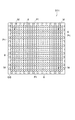
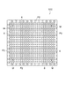
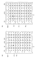
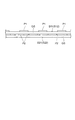
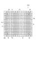
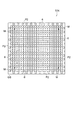
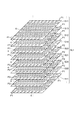
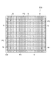
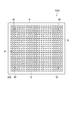
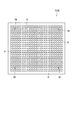
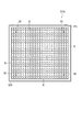
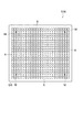
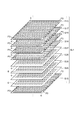
【解決手段】 グリーンシートGSの内側領域に導体パターン6を形成すると共に、外側領域における所定の第1の位置に面状のダミーパターンP1を形成して、第1のシートS11,S12を得る工程と、グリーンシートGSの内側領域に導体パターン6を形成すると共に、外側領域における所定の第2の位置に面状のダミーパターンP2を形成して、第2のシートS21,S22を得る工程とを備える。所定の第1の位置と所定の第2の位置とは、第1のシートS11と第2のシートS21とを重ねた状態で第1及び第2のシートS11,S21の厚み方向から見ると、また、第1のシートS12と第2のシートS22とを重ねた状態で第1及び第2のシートS12,S22の厚み方向から見ると、互いに重ならない位置に設定されている。
【選択図】 図9
Description
Claims (4)
- グリーンシートを用意し、
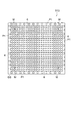
前記グリーンシートの内側領域に線状のパターンを形成すると共に、当該グリーンシートの外側領域における所定の第1の位置に面状のパターンを形成して、第1のシートを得る工程と、
前記グリーンシートの内側領域に線状のパターンを形成すると共に、当該グリーンシートの外側領域における前記所定の第1の位置とは異なる所定の第2の位置に面状のパターンを形成して、第2のシートを得る工程と、
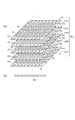
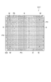
前記第1及び第2のシートを積層し、加圧してシート積層体を得る工程と、
前記シート積層体を切断する工程と、
前記切断したシート積層体を焼成する工程と、を備えることを特徴とする積層型電子部品の製造方法。 - グリーンシートを用意し、
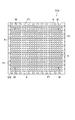
前記グリーンシートの内側領域に線状のパターンを形成すると共に、当該グリーンシートの外側領域に面状のパターンを形成して、当該線状及び面状のパターンが形成された第1のシートを得る工程と、
前記グリーンシートの内側領域に線状のパターンを形成して、当該線状のパターンが形成されると共に前記面状のパターンが形成されていない第2のシートを得る工程と、
前記第1及び第2のシートを積層し、加圧してシート積層体を得る工程と、
前記シート積層体を切断する工程と、
前記切断したシート積層体を焼成する工程と、を備えることを特徴とする積層型電子部品の製造方法。 - 前記第1及び第2のシートを積層する際に、前記第1のシートと前記第2のシートとを交互に積層することを特徴とする請求項1又は請求項2に記載の積層型電子部品の製造方法。
- 前記第1及び第2のシートを積層する際に、前記第1のシートと前記第2のシートとをそれぞれ所定の枚数連続して積層することを特徴とする請求項1又は請求項2に記載の積層型電子部品の製造方法。
Priority Applications (1)
| Application Number | Priority Date | Filing Date | Title |
|---|---|---|---|
| JP2004106699A JP4041086B2 (ja) | 2004-03-31 | 2004-03-31 | 積層型電子部品の製造方法 |
Applications Claiming Priority (1)
| Application Number | Priority Date | Filing Date | Title |
|---|---|---|---|
| JP2004106699A JP4041086B2 (ja) | 2004-03-31 | 2004-03-31 | 積層型電子部品の製造方法 |
Publications (2)
| Publication Number | Publication Date |
|---|---|
| JP2005294487A true JP2005294487A (ja) | 2005-10-20 |
| JP4041086B2 JP4041086B2 (ja) | 2008-01-30 |
Family
ID=35327088
Family Applications (1)
| Application Number | Title | Priority Date | Filing Date |
|---|---|---|---|
| JP2004106699A Expired - Lifetime JP4041086B2 (ja) | 2004-03-31 | 2004-03-31 | 積層型電子部品の製造方法 |
Country Status (1)
| Country | Link |
|---|---|
| JP (1) | JP4041086B2 (ja) |
Cited By (2)
| Publication number | Priority date | Publication date | Assignee | Title |
|---|---|---|---|---|
| US7836935B2 (en) | 2005-11-22 | 2010-11-23 | International Business Machines Corporation | Apparatus for providing uniaxial load distribution for laminate layers of multilayer ceramic chip carriers |
| WO2015056553A1 (ja) * | 2013-10-15 | 2015-04-23 | 株式会社 村田製作所 | 積層型インダクタ素子の製造方法 |
-
2004
- 2004-03-31 JP JP2004106699A patent/JP4041086B2/ja not_active Expired - Lifetime
Cited By (5)
| Publication number | Priority date | Publication date | Assignee | Title |
|---|---|---|---|---|
| US7836935B2 (en) | 2005-11-22 | 2010-11-23 | International Business Machines Corporation | Apparatus for providing uniaxial load distribution for laminate layers of multilayer ceramic chip carriers |
| US7947143B2 (en) | 2005-11-22 | 2011-05-24 | International Business Machines Corporation | Method for providing uniaxial load distribution for laminate layers of multilayer ceramic chip carriers |
| US8156990B2 (en) | 2005-11-22 | 2012-04-17 | International Business Machines Corporation | Apparatus for providing uniaxial load distribution for laminate layers of multilayer ceramic chip carriers |
| WO2015056553A1 (ja) * | 2013-10-15 | 2015-04-23 | 株式会社 村田製作所 | 積層型インダクタ素子の製造方法 |
| JPWO2015056553A1 (ja) * | 2013-10-15 | 2017-03-09 | 株式会社村田製作所 | 積層型インダクタ素子の製造方法、および積層型インダクタ素子 |
Also Published As
| Publication number | Publication date |
|---|---|
| JP4041086B2 (ja) | 2008-01-30 |
Similar Documents
| Publication | Publication Date | Title |
|---|---|---|
| KR101037288B1 (ko) | 적층형 인덕터 및 그 제조 방법 | |
| JP5168234B2 (ja) | 積層型コモンモードフィルタ | |
| KR101490650B1 (ko) | 적층 코일 및 그 제조 방법 | |
| WO2007080680A1 (ja) | インダクタの製造方法 | |
| JP5240221B2 (ja) | 積層型インダクタ、及び積層型インダクタの製造方法 | |
| JPH0855726A (ja) | 積層型電子部品及びその製造方法 | |
| WO2013108862A1 (ja) | コイル部品 | |
| WO2013054587A1 (ja) | 電子部品及びその製造方法 | |
| US11258155B2 (en) | Multilayer electronic component | |
| JP2009238912A (ja) | 積層トランス部品及びその製造方法 | |
| JPH08153623A (ja) | コイル部品 | |
| US11508513B2 (en) | Coil-embedded ceramic substrate | |
| US8143989B2 (en) | Multilayer inductor | |
| US20200075220A1 (en) | Multilayer coil component and method of manufacturing multilayer coil component | |
| JP4780232B2 (ja) | 積層型電子部品 | |
| JP6911369B2 (ja) | 積層コイル部品の製造方法 | |
| JP4041086B2 (ja) | 積層型電子部品の製造方法 | |
| JP2008166385A (ja) | 積層インダクタの製造方法 | |
| JP2009099699A (ja) | 電子部品の製造方法 | |
| JP2006066829A (ja) | 積層型電子部品及びその製造方法 | |
| JP4502130B2 (ja) | 積層電子部品の製造方法 | |
| JPH11354326A (ja) | 積層型インダクタ、及びその製造方法 | |
| JP2006351954A (ja) | 積層型コモンモードフィルタ | |
| JP2009170752A (ja) | 電子部品 | |
| JP4635430B2 (ja) | 積層コイル部品 |
Legal Events
| Date | Code | Title | Description |
|---|---|---|---|
| A131 | Notification of reasons for refusal |
Free format text: JAPANESE INTERMEDIATE CODE: A131 Effective date: 20060912 |
|
| A521 | Request for written amendment filed |
Free format text: JAPANESE INTERMEDIATE CODE: A523 Effective date: 20061106 |
|
| TRDD | Decision of grant or rejection written | ||
| A01 | Written decision to grant a patent or to grant a registration (utility model) |
Free format text: JAPANESE INTERMEDIATE CODE: A01 Effective date: 20071106 |
|
| A61 | First payment of annual fees (during grant procedure) |
Free format text: JAPANESE INTERMEDIATE CODE: A61 Effective date: 20071108 |
|
| FPAY | Renewal fee payment (event date is renewal date of database) |
Free format text: PAYMENT UNTIL: 20101116 Year of fee payment: 3 |
|
| R150 | Certificate of patent or registration of utility model |
Free format text: JAPANESE INTERMEDIATE CODE: R150 Ref document number: 4041086 Country of ref document: JP Free format text: JAPANESE INTERMEDIATE CODE: R150 |
|
| FPAY | Renewal fee payment (event date is renewal date of database) |
Free format text: PAYMENT UNTIL: 20111116 Year of fee payment: 4 |
|
| FPAY | Renewal fee payment (event date is renewal date of database) |
Free format text: PAYMENT UNTIL: 20121116 Year of fee payment: 5 |
|
| FPAY | Renewal fee payment (event date is renewal date of database) |
Free format text: PAYMENT UNTIL: 20121116 Year of fee payment: 5 |
|
| FPAY | Renewal fee payment (event date is renewal date of database) |
Free format text: PAYMENT UNTIL: 20131116 Year of fee payment: 6 |
|
| EXPY | Cancellation because of completion of term |