JP2005294487A - Method of manufacturing laminated electronic component - Google Patents
Method of manufacturing laminated electronic component Download PDFInfo
- Publication number
- JP2005294487A JP2005294487A JP2004106699A JP2004106699A JP2005294487A JP 2005294487 A JP2005294487 A JP 2005294487A JP 2004106699 A JP2004106699 A JP 2004106699A JP 2004106699 A JP2004106699 A JP 2004106699A JP 2005294487 A JP2005294487 A JP 2005294487A
- Authority
- JP
- Japan
- Prior art keywords
- sheet
- sheets
- pattern
- green sheet
- green
- Prior art date
- Legal status (The legal status is an assumption and is not a legal conclusion. Google has not performed a legal analysis and makes no representation as to the accuracy of the status listed.)
- Granted
Links
- 238000004519 manufacturing process Methods 0.000 title claims abstract description 61
- 238000000034 method Methods 0.000 claims description 17
- 238000010030 laminating Methods 0.000 claims description 12
- 238000010304 firing Methods 0.000 claims description 8
- 238000005520 cutting process Methods 0.000 claims description 7
- 238000003825 pressing Methods 0.000 claims description 6
- 239000004020 conductor Substances 0.000 abstract description 77
- 230000002950 deficient Effects 0.000 abstract description 6
- 238000012986 modification Methods 0.000 description 31
- 230000004048 modification Effects 0.000 description 31
- 230000002093 peripheral effect Effects 0.000 description 21
- 230000007547 defect Effects 0.000 description 12
- 230000000052 comparative effect Effects 0.000 description 10
- 229910052759 nickel Inorganic materials 0.000 description 6
- 229910000859 α-Fe Inorganic materials 0.000 description 6
- 239000011230 binding agent Substances 0.000 description 4
- 239000007772 electrode material Substances 0.000 description 4
- 239000011347 resin Substances 0.000 description 4
- 229920005989 resin Polymers 0.000 description 4
- 229910017518 Cu Zn Inorganic materials 0.000 description 3
- 229910017752 Cu-Zn Inorganic materials 0.000 description 3
- 229910017943 Cu—Zn Inorganic materials 0.000 description 3
- 238000001035 drying Methods 0.000 description 3
- 238000003475 lamination Methods 0.000 description 3
- 239000000919 ceramic Substances 0.000 description 2
- 238000009713 electroplating Methods 0.000 description 2
- 229910052737 gold Inorganic materials 0.000 description 2
- 239000000696 magnetic material Substances 0.000 description 2
- 238000005259 measurement Methods 0.000 description 2
- 239000007769 metal material Substances 0.000 description 2
- 229910052763 palladium Inorganic materials 0.000 description 2
- 239000000843 powder Substances 0.000 description 2
- 229910052709 silver Inorganic materials 0.000 description 2
- 239000002002 slurry Substances 0.000 description 2
- 239000002904 solvent Substances 0.000 description 2
- 229910052718 tin Inorganic materials 0.000 description 2
- 229910018072 Al 2 O 3 Inorganic materials 0.000 description 1
- 229920002799 BoPET Polymers 0.000 description 1
- 229910018054 Ni-Cu Inorganic materials 0.000 description 1
- 229910018481 Ni—Cu Inorganic materials 0.000 description 1
- 229910004298 SiO 2 Inorganic materials 0.000 description 1
- 229910009369 Zn Mg Inorganic materials 0.000 description 1
- 229910007573 Zn-Mg Inorganic materials 0.000 description 1
- 239000011324 bead Substances 0.000 description 1
- 229910052802 copper Inorganic materials 0.000 description 1
- TVZPLCNGKSPOJA-UHFFFAOYSA-N copper zinc Chemical compound [Cu].[Zn] TVZPLCNGKSPOJA-UHFFFAOYSA-N 0.000 description 1
- 238000010586 diagram Methods 0.000 description 1
- 230000000694 effects Effects 0.000 description 1
- 238000010292 electrical insulation Methods 0.000 description 1
- 239000002241 glass-ceramic Substances 0.000 description 1
- 230000002706 hydrostatic effect Effects 0.000 description 1
- 238000007689 inspection Methods 0.000 description 1
- 238000004898 kneading Methods 0.000 description 1
- 239000000203 mixture Substances 0.000 description 1
- 230000000149 penetrating effect Effects 0.000 description 1
- 238000007650 screen-printing Methods 0.000 description 1
- 230000000007 visual effect Effects 0.000 description 1
- 238000004804 winding Methods 0.000 description 1
Images


Landscapes
- Fixed Capacitors And Capacitor Manufacturing Machines (AREA)
- Ceramic Capacitors (AREA)
- Manufacturing Cores, Coils, And Magnets (AREA)
- Coils Or Transformers For Communication (AREA)
Abstract
Description
本発明は、積層型電子部品の製造方法に関する。 The present invention relates to a method for manufacturing a multilayer electronic component.
この種の積層型電子部品の製造方法として、電子部品の機能に対応した所望のパターンを形成した複数枚のグリーンシート(例えば、セラミックグリーンシート等)を積層して切断した後に、焼成するものが知られている(例えば、特許文献1参照)。この特許文献1には、均一且つ安定した積層を行える積層型電子部品の製造方法が開示されている。 As a manufacturing method of this type of multilayer electronic component, there is a method in which a plurality of green sheets (for example, ceramic green sheets) having a desired pattern corresponding to the function of the electronic component are stacked and cut and then fired. It is known (see, for example, Patent Document 1). Patent Document 1 discloses a method for manufacturing a multilayer electronic component that can perform uniform and stable lamination.
特許文献1に開示された製造方法は、グリーンシートの中央部領域に、部品機能を実現するための第1のパターンを形成するステップと、上記グリーンシートの周辺部領域に第1のパターンと同様の第2のパターンを形成するステップと、第1および第2のパターンが形成されたグリーンシートを積層し、加圧するステップと、加圧によって得られた成形体を裁断するステップと、裁断した成形体を焼成するステップとを備える。この製造方法によれば、各グリーンシートにおいて、第1のパターンを形成する領域以外の周辺領域にも、第1のパターンと同様のパターンを配置することで、中央部と周辺部での厚さ方向の段差をなくすことができ、シートの積層時における圧着状態が安定化し、より弱い圧力による積層が可能となり、第1のパターンのつぶれ、歪み、および積層のストレスを大幅に緩和できる。
しかしながら、上述した特許文献1に記載された製造方法においては、電子部品の機能に対応した所望のパターンとして線状のパターンをグリーンシートに形成する場合、製造した電子部品に形状不良が発生してしまうという問題を含んでいる。 However, in the manufacturing method described in Patent Document 1 described above, when a linear pattern is formed on a green sheet as a desired pattern corresponding to the function of the electronic component, a defective shape occurs in the manufactured electronic component. The problem of end.
パターンが線状であるが故に、当該パターンとグリーンシートとの接触面積が少ない。このため、線状のパターンを形成したグリーンシートを積層し、加圧すると、グリーンシートにおける線状のパターンが形成された領域に比較的大きな圧力が作用し、当該領域が変形して線状のパターンがグリーンシートに埋もれてしまう。また、線状のパターン自体が潰れて、変形することもある。更には、積層時におけるグリーンシートのズレも生じやすくなる。 Since the pattern is linear, the contact area between the pattern and the green sheet is small. For this reason, when green sheets on which linear patterns are formed are stacked and pressed, a relatively large pressure acts on the areas of the green sheets where the linear patterns are formed, and the areas are deformed to form linear patterns. The pattern is buried in the green sheet. Further, the linear pattern itself may be crushed and deformed. Furthermore, the green sheet is likely to be displaced during lamination.
これに対し、面状のパターンとグリーンシートとの接触面積は比較的大きい。このためグリーンシートにおける面状のパターンが形成された領域に大きな圧力が作用することはなく、面状のパターンはグリーンシートに埋もれ難い。また、面状のパターン自体の変形も殆どない。 On the other hand, the contact area between the planar pattern and the green sheet is relatively large. For this reason, a large pressure does not act on the area | region in which the planar pattern in the green sheet was formed, and the planar pattern is hard to be buried in the green sheet. Further, there is almost no deformation of the planar pattern itself.
したがって、グリーンシートの中央部領域に線状のパターンを形成し、周辺部領域に面状のパターンを形成した場合、両パターンが形成されたグリーンシートを積層して加圧すると、中央部の厚みが周辺部の厚みに比べて薄くなり、成形体が凹状に窪んでしまうこととなる。この結果、切断、焼成することに得られた電子部品に、形状不良(外観不良)が生じてしまうこととなる。また、グリーンシートの周辺部領域に形成するパターンを線状のパターンとした場合、グリーンシートの積層ズレが生じてしまうこととなる。 Therefore, when a linear pattern is formed in the central region of the green sheet and a planar pattern is formed in the peripheral region, the thickness of the central portion is determined by laminating and pressing the green sheets on which both patterns are formed. However, it becomes thinner than the thickness of the peripheral portion, and the molded body will be recessed in a concave shape. As a result, an electronic component obtained by cutting and firing has a shape defect (appearance defect). Further, when the pattern formed in the peripheral region of the green sheet is a linear pattern, the green sheet is misaligned.
本発明の目的は、形状不良の発生を防ぐことが可能な積層型電子部品の製造方法を提供することにある。 An object of the present invention is to provide a method for manufacturing a multilayer electronic component capable of preventing the occurrence of shape defects.
本発明に係る積層型電子部品の製造方法は、グリーンシートを用意し、グリーンシートの内側領域に線状のパターンを形成すると共に、当該グリーンシートの外側領域における所定の第1の位置に面状のパターンを形成して、第1のシートを得る工程と、グリーンシートの内側領域に線状のパターンを形成すると共に、当該グリーンシートの外側領域における所定の第1の位置とは異なる所定の第2の位置に面状のパターンを形成して、第2のシートを得る工程と、第1及び第2のシートを積層し、加圧してシート積層体を得る工程と、シート積層体を切断する工程と、切断したシート積層体を焼成する工程と、を備えることを特徴とする。
In the method for manufacturing a multilayer electronic component according to the present invention, a green sheet is prepared, a linear pattern is formed in an inner region of the green sheet, and a planar shape is formed at a predetermined first position in the outer region of the green sheet. Forming a first pattern, forming a linear pattern in an inner area of the green sheet, and a predetermined first position different from a predetermined first position in the outer area of the green sheet Forming a planar pattern at a
また、本発明に係る積層型電子部品の製造方法は、グリーンシートを用意し、グリーンシートの内側領域に線状のパターンを形成すると共に、当該グリーンシートの外側領域に面状のパターンを形成して、当該線状及び面状のパターンが形成された第1のシートを得る工程と、グリーンシートの内側領域に線状のパターンを形成して、当該線状のパターンが形成されると共に上記面状のパターンが形成されていない第2のシートを得る工程と、第1及び第2のシートを積層し、加圧してシート積層体を得る工程と、シート積層体を切断する工程と、切断したシート積層体を焼成する工程と、を備えることを特徴とする。 Also, in the method for manufacturing a multilayer electronic component according to the present invention, a green sheet is prepared, a linear pattern is formed in an inner region of the green sheet, and a planar pattern is formed in an outer region of the green sheet. A step of obtaining a first sheet on which the linear and planar patterns are formed, a linear pattern is formed on an inner region of the green sheet, and the linear pattern is formed and the surface A step of obtaining a second sheet on which no pattern is formed, a step of laminating and pressurizing the first and second sheets, a step of obtaining a sheet laminate, and a step of cutting the sheet laminate. And a step of firing the sheet laminate.
これら、本発明に係る積層型電子部品の製造方法それぞれにおいて、シート積層体における中央部分(第1及び第2のシートの内側領域に対応する部分)の厚みと周辺部分(第1及び第2のシートの外側領域に対応する部分)の厚みとの差が極めて少なくなる。この結果、シート積層体の中央部分が凹状に窪んでしまうことはなく、切断されたシート積層体に形状不良が発生するのを防ぐことができる。 In each of the multilayer electronic component manufacturing methods according to the present invention, the thickness of the central portion (the portion corresponding to the inner region of the first and second sheets) and the peripheral portion (the first and second portions) in the sheet laminate. The difference from the thickness of the portion corresponding to the outer region of the sheet becomes extremely small. As a result, the central portion of the sheet laminate is not recessed in a concave shape, and it is possible to prevent a defective shape from occurring in the cut sheet laminate.
本発明よれば、形状不良の発生を防ぐことが可能な積層型電子部品の製造方法を提供することにある。 According to the present invention, there is provided a method for manufacturing a multilayer electronic component capable of preventing the occurrence of shape defects.
以下、添付図面を参照して、本発明に係る積層型電子部品の製造方法の好適な実施形態について詳細に説明する。なお、説明において、同一要素又は同一機能を有する要素には、同一符号を用いることとし、重複する説明は省略する。 DESCRIPTION OF EMBODIMENTS Hereinafter, a preferred embodiment of a method for manufacturing a multilayer electronic component according to the present invention will be described in detail with reference to the accompanying drawings. In the description, the same reference numerals are used for the same elements or elements having the same function, and redundant description is omitted.
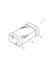
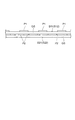
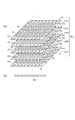
本実施形態は、本発明を積層型インダクタの製造方法に適用したものである。まず、図1及び図2に基づいて、本実施形態に係る積層型インダクタの構成を説明する。図1は、本実施形態に係る積層型インダクタを示す斜視図である。図2は、図1に示された積層型インダクタに含まれる素子の分解斜視図である。 In this embodiment, the present invention is applied to a manufacturing method of a multilayer inductor. First, based on FIG.1 and FIG.2, the structure of the multilayer inductor which concerns on this embodiment is demonstrated. FIG. 1 is a perspective view showing a multilayer inductor according to the present embodiment. FIG. 2 is an exploded perspective view of elements included in the multilayer inductor shown in FIG.
積層型インダクタ1は、直方体形状の素子2と、この素子2の長手方向の両端部に形成された1対の端子電極3,3とを備えている。素子2は、素子本体部4と、該素子本体部4の内部に形成されたコイル部5とから構成されている。コイル部5の両端部に位置する導体パターン5a,5fは、対応する端子電極3,3に電気的に接続されている。
The multilayer inductor 1 includes a rectangular
コイル部5は、線状の導体パターン6が形成された複数枚(例えば、数十枚)のグリーンシート(磁性体グリーンシートあるいは非磁性体グリーンシート)10が積層されることにより構成される。電気絶縁性も有している。素子本体部4は、積層されたグリーンシート10により構成されることとなる。端子電極3,3は、素子2におけるグリーンシート10の積層方向に直交する面に形成されている。
The
導体パターン6は、コイルの略3/4ターン分に相当し、グリーンシート10上で略U字状に形成されている。導体パターン6の端部同士は、グリーンシート10にそれぞれ形成された貫通電極7により電気的に接続される。導体パターン6は、相互に電気的に接続されることで、コイルを構成することとなる。
The
導体パターン5a,5bは、コイルの一方の端部に位置することとなる。線状の導体パターン5cは、貫通電極8aにより導体パターン6と電気的に接続される。導体パターン5a〜5c同士は、貫通電極8cにより電気的に接続される。導体パターン5e,5fは、コイルの他方の端部に位置することとなる。線状の導体パターン5dは、貫通電極8bにより導体パターン6と電気的に接続される。導体パターン5d〜5f同士は、貫通電極8dにより電気的に接続される。
The
次に、図3〜図9を参照して、本実施形態に係る積層型インダクタ1の製造過程について説明する。図3〜図9は、本実施形態に係る積層型インダクタの製造過程を説明するための図である。 Next, a manufacturing process of the multilayer inductor 1 according to the present embodiment will be described with reference to FIGS. 3 to 9 are views for explaining a manufacturing process of the multilayer inductor according to the present embodiment.
まず、グリーンシートGS(いわゆるセラミックグリーンシート)を作製して、用意する(図3〜図6参照)。ここでは、Ni−Cu−Zn系フェライト、Ni−Cu−Zn−Mg系フェライト、Cu−Zn系フェライト、Ni−Cu系フェライト等の磁性体材料、あるいは、ガラス系セラミック(例えば、Sr、Ca、Al2O3、SiO2等を含む)等の非磁性体材料を用い、公知の手法によりグリーンシートGSを作製する。グリーンシートGSは、例えば、例えばNi−Cu−Zn系フェライト粉末に、バインダー樹脂(例えば、有機バインダー樹脂等)と溶剤とを加えて混錬することにより得たスラリーを、PETフィルム上にドクターブレード法により塗布し、乾燥させることにより得ることができる。乾燥後におけるグリーンシートGSの厚みは、例えば20μm程度である。 First, a green sheet GS (so-called ceramic green sheet) is prepared and prepared (see FIGS. 3 to 6). Here, a magnetic material such as Ni—Cu—Zn ferrite, Ni—Cu—Zn—Mg ferrite, Cu—Zn ferrite, Ni—Cu ferrite, or glass ceramic (for example, Sr, Ca, A green sheet GS is produced by a known method using a non-magnetic material such as Al 2 O 3 or SiO 2 . The green sheet GS is, for example, a slurry obtained by adding a binder resin (for example, organic binder resin) and a solvent to a Ni—Cu—Zn ferrite powder and kneading the slurry onto a PET film. It can be obtained by applying and drying by the method. The thickness of the green sheet GS after drying is, for example, about 20 μm.
続いて、グリーンシートGSの所定の位置、すなわち貫通電極7,8a〜8dを形成する予定位置に、レーザー加工等によってスルーホールを形成する(図示略)。
Subsequently, through holes are formed by laser processing or the like (not shown) at predetermined positions on the green sheet GS, that is, positions where the through
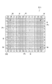
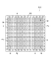
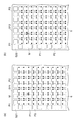
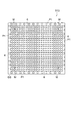
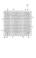
次に、上記グリーンシートGSに対応する導体パターン5a〜5f,6を形成する。この過程では、グリーンシートGSの内側領域に導体パターン6を複数形成すると共に、外側領域における所定の第1の位置に複数の面状のダミーパターンP1を形成して、第1のシートS11,S12を得る工程(図3及び図4参照)と、グリーンシートGSの内側領域に導体パターン6を複数形成すると共に、外側領域における上記所定の第1の位置とは異なる所定の第2の位置に複数の面状のダミーパターンP2を形成して、第2のシートS21,S22を得る工程(図5及び図6参照)とを含んでいる。
Next,
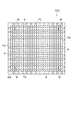
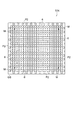
導体パターン6は、M行N列(パラメータM及びNそれぞれを2以上の整数とする)に2次元配列されている。第1のシートS11と第1のシートS12とは、導体パターン6が異なっている。すなわち、第1のシートS11の導体パターン6と第1のシートS12の導体パターン6とは、その向きが180°ずれている。また、第2のシートS21と第2のシートS22とも、導体パターン6が異なっている。すなわち、第2のシートS21の導体パターン6と第2のシートS22の導体パターン6とは、その向きが180°ずれている。第1のシートS11の導体パターン6と第2のシートS21の導体パターン6とは、また、第1のシートS12の導体パターン6と第2のシートS22の導体パターン6とは、その向きがそれぞれ90°ずれている。
The
また、この過程では、対応するグリーンシートGSの内側領域に導体パターン5a〜5cをそれぞれ複数形成して、導体パターン5a〜5cのそれぞれに対応する複数の第3のシートを得る工程、及び、対応するグリーンシートGSの内側領域に導体パターン5d〜5fをそれぞれ複数形成して、導体パターン5d〜5fのそれぞれに対応する複数の第4のシートを得る工程も含んでいる(いずれも、図示略)。また、第1〜第4のシートS11,S12,S21,S22,…には、積層する際に位置を合わせるためのターゲットマークMも形成される。
Further, in this process, a plurality of
導体パターン5a〜5f,6、ダミーパターンP1,P2、及びターゲットマークMは、例えば、電極材料をスクリーン印刷した後、乾燥させることによって形成される。電極材料は、導電性を有する金属材料と、バインダー樹脂(例えば、有機バインダー樹脂等)と、溶剤とを混合したペースト状の組成物である。金属材料としては、Ag粉を用いることができる。導体パターン5a〜5f,6を印刷する際に、スルーホールに電極材料が充填され、当該スルーホールに充填された電極材料により貫通電極7,8a〜8dが形成されることとなる。
The
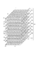
上記所定の第1の位置と所定の第2の位置とは、第1のシートS11と第2のシートS21とを重ねた状態で第1及び第2のシートS11,S21の厚み方向から見ると、また、第1のシートS12と第2のシートS22とを重ねた状態で第1及び第2のシートS12,S22の厚み方向から見ると、互いに重ならない位置に設定されている(図7(a)及び(b)参照)。これにより、ダミーパターンP1とダミーパターンP2とは、第1のシートS11と第2のシートS21とを重ねた状態で第1及び第2のシートS11,S21の厚み方向から見ると、また、第1のシートS12と第2のシートS22とを重ねた状態で第1及び第2のシートS12,S22の厚み方向から見ると、交互に並ぶように形成されることとなる。また、第1のシートS11と第2のシートS21とを重ねた状態で第1及び第2のシートS11,S21の厚み方向に直行する方向から見ると、また、第1のシートS12と第2のシートS22とを重ねた状態で第1及び第2のシートS12,S22の厚み方向に直行する方向から見ると、ダミーパターンP1とダミーパターンP2とは、千鳥状に形成されることとなる(図8参照)。 The predetermined first position and the predetermined second position are viewed from the thickness direction of the first and second sheets S11 and S21 in a state where the first sheet S11 and the second sheet S21 are overlapped. Further, when viewed from the thickness direction of the first and second sheets S12 and S22 in a state where the first sheet S12 and the second sheet S22 are overlapped, they are set to positions that do not overlap each other (FIG. 7 ( a) and (b)). Thereby, when the dummy pattern P1 and the dummy pattern P2 are viewed from the thickness direction of the first and second sheets S11 and S21 in a state where the first sheet S11 and the second sheet S21 are overlapped, When viewed from the thickness direction of the first and second sheets S12 and S22 in a state where the first sheet S12 and the second sheet S22 are overlapped, they are formed so as to be alternately arranged. Further, when viewed from the direction orthogonal to the thickness direction of the first and second sheets S11 and S21 with the first sheet S11 and the second sheet S21 being overlapped, the first sheet S12 and the second sheet S21 When viewed from the direction perpendicular to the thickness direction of the first and second sheets S12 and S22 in a state where the sheet S22 is overlaid, the dummy pattern P1 and the dummy pattern P2 are formed in a staggered pattern ( (See FIG. 8).
その後、第1〜第4のシートS11,S12,S21,S22,…を所望の大きさ(例えば、130mm×150mm程度)に切断する。ダミーパターンP1,P2は、切断されたグリーンシートGSの各辺に沿って併設されることとなる。なお、図3〜図6では、第1及び第2のシートS11,S12,S21,S22は、所望の大きさに切断した後の状態で示されている。 Thereafter, the first to fourth sheets S11, S12, S21, S22,... Are cut into a desired size (for example, about 130 mm × 150 mm). The dummy patterns P1, P2 are provided along each side of the cut green sheet GS. 3 to 6, the first and second sheets S11, S12, S21, and S22 are shown in a state after being cut to a desired size.
次に、第1〜第4のシートS11,S12,S21,S22,…を積層し、加圧して、圧着させる。これにより、シート積層体SL1が得られることとなる。ここでは、まず、第4のシートを積層する。そして、この第4のシートの上に、第1のシートS11,S12及び第2のシートS21,S22を交互に積層する。詳細には、第1のシートS11、第2のシートS21、第1のシートS12、第2のシートS22の順に連続するように積層する(図9(a)参照)。 Next, the first to fourth sheets S11, S12, S21, S22,... Thereby, sheet laminated body SL1 will be obtained. Here, first, the fourth sheet is laminated. Then, the first sheets S11 and S12 and the second sheets S21 and S22 are alternately laminated on the fourth sheet. Specifically, the first sheet S11, the second sheet S21, the first sheet S12, and the second sheet S22 are laminated in this order (see FIG. 9A).
更に、交互に積層した第1のシートS11,S12及び第2のシートS21,S22の上に第3のシートを積層する。積層した第1〜第4のシートS11,S12,S21,S22,…の加圧には、静水圧プレス法を用いることができる。また、積層した第1〜第4のシートS11,S12,S21,S22,…に加える圧力は、例えば、65〜100MPa程度とするのが好ましい。 Further, a third sheet is laminated on the first sheets S11 and S12 and the second sheets S21 and S22 that are alternately laminated. A hydrostatic press method can be used for pressurization of the laminated first to fourth sheets S11, S12, S21, S22,. Moreover, it is preferable that the pressure added to the laminated | stacked 1st-4th sheet | seat S11, S12, S21, S22, ... is about 65-100 Mpa, for example.
第1及び第2のシートS11,S12,S21,S22のスルーホール(貫通電極7)は、隣り合う導体パターン6の端部同士が重なる場所に形成されており、導体パターン6が第1及び第2のシートS11,S12,S21,S22の積層により貫通電極7を介して螺旋状に接続されるようになっている。
The through holes (penetrating electrodes 7) of the first and second sheets S11, S12, S21, and S22 are formed where the ends of the
次に、シート積層体SL1を所定の形状・大きさに切断する(図示略)。シート積層体SL1は、一般に端子電極3,3の形成された位置が特定し易いように直方体とし、例えば、焼成後に直方体の長手方向の長さが1.6mm、直方体の幅と高さが0.8mm程度となるように切断する。なお、シート積層体SL1におけるダミーパターンP1,P2が形成された部分は、積層型インダクタ1の機能に必要とされない部分であり、廃棄される。切断されたシート積層体SL1に含まれる第1〜第4のシートS11,S12,S21,S22,…のグリーンシートGSが、上述したグリーンシート10を構成することとなる。
Next, the sheet laminate SL1 is cut into a predetermined shape and size (not shown). The sheet laminate SL1 is generally a rectangular parallelepiped so that the positions where the
次に、切断したシート積層体SL1を所定の温度で焼成する(図示略)。これにより、素子2が得られることとなる。焼成の温度は、例えば、870℃程度とする。
Next, the cut sheet laminate SL1 is fired at a predetermined temperature (not shown). Thereby, the
次に、素子2の導体パターン6が露出した端面に端子電極3,3を形成する(図示略)。ここでは、Agを主成分とする導体ペーストを塗布した後に、所定温度(例えば、700℃程度)にて焼き付け、更に電気めっきを施すことによって端子電極3,3を形成する。電気めっきには、CuとNiとSn、NiとSn、NiとAu、NiとPdとAu、NiとPdとAg、又は、NiとAg等を用いることができる。
Next,
これらの過程を経て、図1及び図2に示された構成を有する積層型インダクタ1が完成する。 Through these processes, the multilayer inductor 1 having the configuration shown in FIGS. 1 and 2 is completed.
各ダミーパターンP101が、図28(a)に示されるように、シートS111,S112,S121,S122における同じ位置に形成されている場合、これらのシートS111,S112,S121,S122を含むシート積層体SL2では、シートS111,S112,S121,S122の厚み方向から見て、ダミーパターンP101が重なってしまう。このため、シート積層体SL2における中央部分(シートS111,S112,S121,S122の内側領域、すなわち導体パターン6が形成された領域に対応する部分)の厚みが周辺部分(シートS111,S112,S121,S122の外側領域、すなわちダミーパターンP101が形成された領域に対応する部分)の厚みに比べて薄くなる。この結果、シート積層体SL2の中央部分が凹状に窪んでしまうこととなり(図28(b)参照)、切断されたシート積層体SL2に形状不良が発生する。
When each dummy pattern P101 is formed at the same position in the sheets S111, S112, S121, and S122 as shown in FIG. 28A, the sheet laminate including these sheets S111, S112, S121, and S122. In SL2, the dummy pattern P101 overlaps when viewed from the thickness direction of the sheets S111, S112, S121, and S122. For this reason, the thickness of the central portion (the inner region of the sheets S111, S112, S121, S122, that is, the portion corresponding to the region where the
これに対して、本実施形態においては、各ダミーパターンP1,P2が、第1のシートS11,S12と第2のシートS21,S22とを重ねた状態で第1及び第2のシートS11,S12,S21,S22の厚み方向から見ると、互いに重ならない位置に形成されている。このため、シート積層体SL1における中央部分(第1及び第2のシートS11,S12,S21,S22の内側領域、すなわち導体パターン6が形成された領域に対応する部分)の厚みと周辺部分(第1及び第2のシートS11,S12,S21,S22の外側領域、すなわちダミーパターンP1,P2が形成された領域に対応する部分)の厚みとの差が極めて少なくなる。この結果、シート積層体SL1の中央部分が凹状に窪んでしまうことはなく(図9(b)参照)、切断されたシート積層体SL1に形状不良が発生するのを防ぐことができる。
On the other hand, in the present embodiment, each of the dummy patterns P1 and P2 has the first and second sheets S11 and S12 in a state where the first sheets S11 and S12 and the second sheets S21 and S22 are overlapped. , S21 and S22 are formed at positions that do not overlap each other when viewed from the thickness direction. For this reason, the thickness and the peripheral portion (the first portion corresponding to the inner region of the first and second sheets S11, S12, S21, and S22, that is, the region where the
また、本実施形態においては、各ダミーパターンP1,P2が面状とされているので、積層する際に、隣接する第1及び第2のシートS11,S12,S21,S22との接着性が安定し、積層ズレの発生を防止できる。 In the present embodiment, since the dummy patterns P1 and P2 have a planar shape, the adhesion between the adjacent first and second sheets S11, S12, S21, and S22 is stable when stacked. In addition, the occurrence of misalignment can be prevented.
以上のことから、本実施形態に係る製造方法によれば、積層型インダクタ1に形状不良(外観不良)が発生するのを防ぐことができる。 From the above, according to the manufacturing method according to the present embodiment, it is possible to prevent the multilayer inductor 1 from being defective in shape (defective appearance).
次に、図10〜図26を参照して、本実施形態に係る積層型インダクタの製造方法の変形例について説明する。 Next, with reference to FIGS. 10 to 26, a modified example of the manufacturing method of the multilayer inductor according to the present embodiment will be described.
図10〜図14は、本実施形態に係る積層型インダクタの製造過程の一変形例を説明するための図である。図10〜図13では、第1及び第2のシートS11〜S14,S21〜S24は、所望の大きさに切断した後の状態で示されている。 10 to 14 are diagrams for explaining a modification of the manufacturing process of the multilayer inductor according to the present embodiment. 10 to 13, the first and second sheets S11 to S14 and S21 to S24 are shown in a state after being cut to a desired size.
本変形例に係る製造方法では、グリーンシートGSの外側領域における所定の第1の位置にダミーパターンP1を形成した第1のシートS11,S12,S13,S14(図3、図4、図10及び図11参照)と、グリーンシートGSの外側領域における所定の第2の位置にダミーパターンP2を形成した第2のシートS21,S22,S23,S24(図5、図6、図12及び図13参照)とを作製する。そして、第1及び第2のシートS11〜S14,S21〜S24を積層する際に、ダミーパターンP1を形成した第1のシートS11〜S14が連続すると共に、ダミーパターンP2を形成した第2のシートS21〜S24が連続するように積層する(図14参照)。 In the manufacturing method according to this modification, the first sheets S11, S12, S13, and S14 in which the dummy pattern P1 is formed at a predetermined first position in the outer region of the green sheet GS (FIGS. 3, 4, 10, and 10) 11) and second sheets S21, S22, S23, S24 (see FIGS. 5, 6, 12, and 13) in which a dummy pattern P2 is formed at a predetermined second position in the outer region of the green sheet GS. ). And when laminating | stacking 1st and 2nd sheet | seat S11-S14, S21-S24, while the 1st sheet | seat S11-S14 which formed dummy pattern P1 continued, the 2nd sheet | seat which formed dummy pattern P2 Lamination is performed so that S21 to S24 are continuous (see FIG. 14).
第1のシートS13における導体パターン6の向きは、第2のシートS21における導体パターン6の向きと同じである。第1のシートS14における導体パターン6の向きは、第2のシートS22における導体パターン6の向きと同じである。第2のシートS23における導体パターン6の向きは、第1のシートS11における導体パターン6の向きと同じである。第2のシートS24における導体パターン6の向きは、第1のシートS12における導体パターン6の向きと同じである。
The direction of the
ダミーパターンP1が形成された第1のシートS11〜S14を連続して積層する枚数、及び、ダミーパターンP2が形成された第2のシートS21〜S24を連続して積層する枚数は、図14に示した4枚に限られるものではない。例えば、それぞれのシートS11〜S14,S21〜S24を2枚又は3枚連続させて積層してもよい。また、それぞれのシートS11〜S14,S21〜S24を5枚以上連続させて積層してもよい。 The number of sheets on which the first sheets S11 to S14 on which the dummy pattern P1 is formed is continuously laminated and the number of sheets on which the second sheets S21 to S24 on which the dummy pattern P2 are formed are continuously laminated are shown in FIG. It is not limited to the four shown. For example, each of the sheets S11 to S14 and S21 to S24 may be laminated in succession by two sheets or three sheets. Further, five or more sheets S11 to S14 and S21 to S24 may be continuously stacked.
本変形例に係る製造方法においても、第1及び第2のシートS11〜S14,S21〜S24の厚み方向から見て、ダミーパターンP1,P2が互いに重ならないため、シート積層体SL1における中央部分の厚みと周辺部分の厚みとの差が極めて少なくなる。また、本変形例においても、各ダミーパターンP1,P2が面状とされているので、第1及び第2のシートS11,S12,S21,S22の積層ズレの発生を防止できる。 Also in the manufacturing method according to this modification, the dummy patterns P1 and P2 do not overlap each other when viewed from the thickness direction of the first and second sheets S11 to S14 and S21 to S24. The difference between the thickness and the thickness of the peripheral portion is extremely reduced. Also in this modified example, since each dummy pattern P1, P2 has a planar shape, it is possible to prevent occurrence of stacking misalignment of the first and second sheets S11, S12, S21, S22.
図15〜図21は、本実施形態に係る積層型インダクタの製造過程の一変形例を説明するための図である。図15〜図20では、第1及び第2のシートS15,S16,S25,S26は、所望の大きさに切断した後の状態で示されている。 15 to 21 are views for explaining a modification of the manufacturing process of the multilayer inductor according to the present embodiment. 15 to 20, the first and second sheets S15, S16, S25, and S26 are shown in a state after being cut into a desired size.
本変形例に係る製造方法は、グリーンシートGSの内側領域に導体パターン6を複数形成すると共に、外側領域に複数の面状のダミーパターンP3を形成して、導体パターン6及びダミーパターンP3が形成された第1のシートS15,S16を得る工程(図15及び図16参照)と、グリーンシートGSの内側領域に導体パターン6を複数形成して、導体パターン6が形成されると共にダミーパターンP3が形成されていない第2のシートS25,S26を得る工程(図17及び図18参照)とを含んでいる。ダミーパターンP3は、グリーンシートGSの各辺に沿って伸びるように形成してもよく(図19参照)、また、グリーンシートGSの内側領域を囲むように形成してもよい(図20参照)。シートを積層する際に空気の抜け道を確保してシート同士を密着させるために、グリーンシートGSの内側領域を完全に囲んでしまわないように、ダミーパターンP3を形成することが好ましい。ダミーパターンP3は、切断されたグリーンシートGSの各辺に沿って併設されている。
In the manufacturing method according to this modification, a plurality of
第1のシートS15における導体パターン6の向きは、第1のシートS11における導体パターン6の向きと同じである。第1のシートS16における導体パターン6の向きは、第1のシートS12における導体パターン6の向きと同じである。第2のシートS25における導体パターン6の向きは、第2のシートS21における導体パターン6の向きと同じである。第2のシートS26における導体パターン6の向きは、第2のシートS22における導体パターン6の向きと同じである。
The direction of the
第1及び第2のシートS15,S16,S25,S26を積層する際に、導体パターン6及びダミーパターンP3が形成された第1のシートS15,S16と、導体パターン6が形成されると共にダミーパターンP3が形成されていない第2のシートS25,S26とを交互に積層する(図21(a)参照)。
When the first and second sheets S15, S16, S25, and S26 are laminated, the first sheets S15 and S16 on which the
本変形例においては、ダミーパターンP3が形成された第1のシートS15,S16とダミーパターンP3が形成されていない第2のシートS25,S26とが積層されるので、シート積層体SL1における中央部分の厚みと周辺部分の厚みとの差が極めて少なくなる(図21(b)参照)。 In the present modification, the first sheet S15, S16 on which the dummy pattern P3 is formed and the second sheet S25, S26 on which the dummy pattern P3 is not formed are laminated, so that the central portion in the sheet laminate SL1 The difference between the thickness of the film and the thickness of the peripheral portion is extremely small (see FIG. 21B).
図22〜図26は、本実施形態に係る積層型インダクタの製造過程の一変形例を説明するための図である。図22〜図25では、第1及び第2のシートS15〜S18,S25〜S28は、所望の大きさに切断した後の状態で示されている。 22 to 26 are views for explaining a modification of the manufacturing process of the multilayer inductor according to the present embodiment. 22 to 25, the first and second sheets S15 to S18 and S25 to S28 are shown in a state after being cut to a desired size.
本変形例に係る製造方法は、グリーンシートGSの内側領域に導体パターン6を複数形成し、外側領域に面状のダミーパターンP3を形成して、導体パターン6及びダミーパターンP3が形成された第1のシートS15,S16,S17,S18を得る工程(図15、図16、図22及び図23参照)と、グリーンシートGSの内側領域に導体パターン6を複数形成して、導体パターン6が形成されると共にダミーパターンP3が形成されていない第2のシートS25,S26,S27,S28を得る工程(図17、図18、図24及び図25参照)とを含んでいる。ダミーパターンP3は、切断されたグリーンシートGSの各辺に沿って併設されることとなる。そして、第1及び第2のシートS15〜S18,S25〜S28を積層する際に、ダミーパターンP3が形成された第1のシートS15〜S18が連続すると共に、ダミーパターンP3が形成されていない第2のシートS25〜S28が連続するように積層する(図26参照)。
In the manufacturing method according to this modification, a plurality of
第1のシートS17における導体パターン6の向きは、第2のシートS25における導体パターン6の向きと同じである。第1のシートS18における導体パターン6の向きは、第2のシートS26における導体パターン6の向きと同じである。第2のシートS27における導体パターン6の向きは、第1のシートS15における導体パターン6の向きと同じである。第2のシートS28における導体パターン6の向きは、第1のシートS16における導体パターン6の向きと同じである。
The direction of the
ダミーパターンP3が形成された第1のシートS15〜S18を連続して積層する枚数、及び、ダミーパターンP3が形成されていない第2のシートS25〜S28を連続して積層する枚数は、図26に示した4枚に限られるものではない。例えば、それぞれのシートS15〜S18,S25〜S28を2枚又は3枚連続させて積層してもよい。また、それぞれのシートS15〜S18,S25〜S28を5枚以上連続させて積層してもよい。 The number of the first sheets S15 to S18 on which the dummy pattern P3 is formed is continuously laminated, and the number of the second sheets S25 to S28 on which the dummy pattern P3 is not continuously laminated are as shown in FIG. It is not limited to the four shown in. For example, each of the sheets S15 to S18 and S25 to S28 may be laminated in succession by two sheets or three sheets. Further, five or more sheets S15 to S18 and S25 to S28 may be continuously stacked.
本変形例においては、ダミーパターンP3が形成された第1のシートS15〜S18と、ダミーパターンP3が形成されていない第2のシートS25〜S28とが積層されるので、シート積層体SL1における中央部分の厚みと周辺部分の厚みとの差が極めて少なくなる。 In the present modification, the first sheets S15 to S18 on which the dummy pattern P3 is formed and the second sheets S25 to S28 on which the dummy pattern P3 is not formed are stacked, so that the center in the sheet stack SL1 The difference between the thickness of the portion and the thickness of the peripheral portion is extremely reduced.
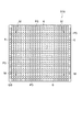
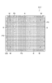
ここで、本実施形態によって、形状不良の発生を防ぐことができることを、実施例1及び2と比較例1及び2とによって、具体的に示す。実施例1及び2と比較例1及び2とでは、シート積層体における中心部の厚みと周辺部との厚みとの差を測定した。各例とも、シート積層体のサンプル数を22個とした。また、周辺部における厚みの測定箇所は、各例とも、図27において黒塗り三角のシンボルにて示される、所定の8ヵ所とした。 Here, it is specifically shown by Examples 1 and 2 and Comparative Examples 1 and 2 that the present embodiment can prevent the occurrence of shape defects. In Examples 1 and 2 and Comparative Examples 1 and 2, the difference between the thickness of the central portion and the thickness of the peripheral portion in the sheet laminate was measured. In each example, the number of samples of the sheet laminate was set to 22. In addition, the thickness measurement locations in the peripheral portion were set at eight predetermined locations indicated by black triangle symbols in FIG.
実施例1では、上述した実施形態に係る製造方法に基づいて得たシート積層体SL1を用いた。実施例2では、図15〜図18、及び図21に示される本実施形態に係る製造方法の変形例に基づいて得たシート積層体SL1を用いた。比較例1では、第1及び第2のシートS11,S12,S21,S22をダミーパターンP1,P2が形成されていない第1及び第2のシートに変更して作製したシート積層体を用いた。比較例2では、図28に示されるように、ダミーパターンP101が同じ位置に形成されたシートS111,S112,S121,S122により作製したシート積層体SL2を用いた。 In Example 1, sheet laminated body SL1 obtained based on the manufacturing method which concerns on embodiment mentioned above was used. In Example 2, sheet laminated body SL1 obtained based on the modification of the manufacturing method which concerns on this embodiment shown by FIGS. 15-18 and FIG. 21 was used. In the comparative example 1, the sheet | seat laminated body produced by changing the 1st and 2nd sheet | seat S11, S12, S21, S22 into the 1st and 2nd sheet | seat in which the dummy patterns P1 and P2 are not formed was used. In Comparative Example 2, as shown in FIG. 28, a sheet laminate SL2 produced by sheets S111, S112, S121, and S122 having dummy patterns P101 formed at the same position was used.
実施例1のシート積層体SL1における中心部の厚みと周辺部との厚みとの差は、約4μm以下であった。実施例2のシート積層体SL1における中心部の厚みと周辺部との厚みとの差は、約−6μm以下であった。比較例1のシート積層体における中心部の厚みと周辺部との厚みとの差は、約−21μm以下であった。比較例2のシート積層体SL2における中心部の厚みと周辺部との厚みとの差は、約24μm以下であった。なお、シート積層体SL1,SL2,…における周辺部の厚みが中心部の厚みに比べて薄い場合に、上記差は負の値となる。 The difference between the thickness of the central portion and the thickness of the peripheral portion in the sheet laminate SL1 of Example 1 was about 4 μm or less. The difference between the thickness of the central portion and the thickness of the peripheral portion in the sheet laminate SL1 of Example 2 was about −6 μm or less. The difference between the thickness of the central portion and the thickness of the peripheral portion in the sheet laminate of Comparative Example 1 was about −21 μm or less. The difference between the thickness of the central portion and the thickness of the peripheral portion in the sheet laminate SL2 of Comparative Example 2 was about 24 μm or less. In addition, when the thickness of the peripheral part in sheet | seat laminated body SL1, SL2, ... is thin compared with the thickness of a center part, the said difference becomes a negative value.
このように、実施例1及び2は、比較例1及び2に比べて、シート積層体SL1における中心部の厚みと周辺部との厚みとの差が極めて小さい。以上のことから、本実施形態の有効性が確認された。 As described above, in Examples 1 and 2, the difference between the thickness of the central portion and the thickness of the peripheral portion in the sheet laminate SL1 is extremely small as compared with Comparative Examples 1 and 2. From the above, the effectiveness of the present embodiment was confirmed.
続いて、各例にて用いたシート積層体SL1,SL2,…からそれぞれ積層型インダクタを作製し、目視による外観不良検査(検体数:2万個)を実施した。なお、焼成後における導体パターン6の幅及び厚みは、それぞれ80μm及び14μmとした。また、導体パターン6により形成されるコイルのターン数は、7.5ターンとした。
Subsequently, multilayer inductors were produced from the sheet laminates SL1, SL2,... Used in each example, and a visual appearance defect inspection (the number of specimens: 20,000) was performed. In addition, the width | variety and thickness of the
実施例1にて用いたシート積層体SL1から作製した積層型インダクタの外観不良率は、約0.014%であった。実施例2にて用いたシート積層体SL1から作製した積層型インダクタの外観不良率は、約0.019%であった。比較例1にて用いたシート積層体から作製した積層型インダクタの外観不良率は、約1.24%であった。比較例2にて用いたシート積層体SL2から作製した積層型インダクタの外観不良率は、約1.64%であった。 The appearance defect rate of the multilayer inductor produced from the sheet laminate SL1 used in Example 1 was about 0.014%. The appearance defect rate of the multilayer inductor produced from the sheet laminate SL1 used in Example 2 was about 0.019%. The appearance defect rate of the multilayer inductor produced from the sheet laminate used in Comparative Example 1 was about 1.24%. The appearance defect rate of the multilayer inductor produced from the sheet laminate SL2 used in Comparative Example 2 was about 1.64%.
このように、実施例1及び2は、比較例1及び2に比べて、外観不良率が極めて小さい。以上のことからも、本実施形態の有効性が確認された。 Thus, Examples 1 and 2 have a very small appearance defect rate compared to Comparative Examples 1 and 2. From the above, the effectiveness of the present embodiment was confirmed.
以上、本発明の好適な実施形態について詳細に説明したが、本発明は上記実施形態及び変形例に限定されるものではない。例えば、ダミーパターンP1〜P3も、上述した実施形態及び変形例にて示された矩形形状に限られことなく、面状であれば他の形状であってもよい。また、導体パターン6は、略U字状に限られることなく、略C字状、略I字状、略J字状、略L字状、又は、スパイラル状等の形状であってもよい。また、本実施形態及び変形例では、第1のシートS11,S15及び第2のシートS23,S27と、第1のシートS12,S16及び第2のシートS24,S28と、第1のシートS13,S17及び第2のシートS21,S25と、第1のシートS14,S18及び第2のシートS22,S26との4種類のシートを作製しているが、これに限られることなく、導体パターン6の形状(例えば、向き等)に対応した種類数のシートを作製すればよい。
Although the preferred embodiments of the present invention have been described in detail above, the present invention is not limited to the above-described embodiments and modifications. For example, the dummy patterns P <b> 1 to P <b> 3 are not limited to the rectangular shapes shown in the above-described embodiments and modifications, but may be other shapes as long as they are planar. The
また、本発明は、端子電極3,3が素子2におけるグリーンシートの積層方向に直交する面に形成された、いわゆる縦巻き型の積層型インダクタに限られることなく、端子電極3,3が素子2におけるグリーンシートの積層方向に平行な面に形成された積層型インダクタにも適用できる。更に、本発明は、積層型インダクタに限らず、フェライトビーズ、コモンモードフィルタ、3端子フィルタ等の積層型電子部品に適用しても同様の効果を得ることができる。
Further, the present invention is not limited to the so-called vertical winding type multilayer inductor in which the
1…積層型インダクタ、2…素子、3,3…端子電極、4…素子本体部、5…コイル部、5a〜5f,6…導体パターン、7,8a〜8d…貫通電極、10,GS…グリーンシート、P1〜P3,P101…ダミーパターン、S11〜S18…第1のシート、S21〜S28…第2のシート、SL1,SL2…シート積層体。
DESCRIPTION OF SYMBOLS 1 ... Multilayer inductor, 2 ... Element, 3, 3 ... Terminal electrode, 4 ... Element main body part, 5 ... Coil part, 5a-5f, 6 ... Conductor pattern, 7, 8a-8d ... Through electrode, 10, GS ... Green sheet, P1-P3, P101 ... dummy pattern, S11-S18 ... first sheet, S21-S28 ... second sheet, SL1, SL2 ... sheet laminate.
Claims (4)
前記グリーンシートの内側領域に線状のパターンを形成すると共に、当該グリーンシートの外側領域における所定の第1の位置に面状のパターンを形成して、第1のシートを得る工程と、
前記グリーンシートの内側領域に線状のパターンを形成すると共に、当該グリーンシートの外側領域における前記所定の第1の位置とは異なる所定の第2の位置に面状のパターンを形成して、第2のシートを得る工程と、
前記第1及び第2のシートを積層し、加圧してシート積層体を得る工程と、
前記シート積層体を切断する工程と、
前記切断したシート積層体を焼成する工程と、を備えることを特徴とする積層型電子部品の製造方法。 Prepare a green sheet,
Forming a linear pattern in the inner region of the green sheet and forming a planar pattern at a predetermined first position in the outer region of the green sheet to obtain a first sheet;
Forming a linear pattern in an inner region of the green sheet and forming a planar pattern in a predetermined second position different from the predetermined first position in the outer region of the green sheet; Obtaining two sheets;
Laminating the first and second sheets and applying pressure to obtain a sheet laminate;
Cutting the sheet laminate,
And a step of firing the cut sheet laminate. A method for manufacturing a multilayer electronic component, comprising:
前記グリーンシートの内側領域に線状のパターンを形成すると共に、当該グリーンシートの外側領域に面状のパターンを形成して、当該線状及び面状のパターンが形成された第1のシートを得る工程と、
前記グリーンシートの内側領域に線状のパターンを形成して、当該線状のパターンが形成されると共に前記面状のパターンが形成されていない第2のシートを得る工程と、
前記第1及び第2のシートを積層し、加圧してシート積層体を得る工程と、
前記シート積層体を切断する工程と、
前記切断したシート積層体を焼成する工程と、を備えることを特徴とする積層型電子部品の製造方法。 Prepare a green sheet,
A linear pattern is formed in the inner area of the green sheet, and a planar pattern is formed in the outer area of the green sheet to obtain a first sheet on which the linear and planar patterns are formed. Process,
Forming a linear pattern in an inner region of the green sheet to obtain a second sheet in which the linear pattern is formed and the planar pattern is not formed;
Laminating the first and second sheets and applying pressure to obtain a sheet laminate;
Cutting the sheet laminate,
And a step of firing the cut sheet laminate. A method for manufacturing a multilayer electronic component, comprising:
The said 1st sheet | seat and the said 2nd sheet | seat are each laminated | stacked a predetermined number of sheets continuously when laminating | stacking the said 1st and 2nd sheet | seat, The Claim 1 or Claim 2 characterized by the above-mentioned. Manufacturing method for multilayer electronic components.
Priority Applications (1)
| Application Number | Priority Date | Filing Date | Title |
|---|---|---|---|
| JP2004106699A JP4041086B2 (en) | 2004-03-31 | 2004-03-31 | Manufacturing method of multilayer electronic component |
Applications Claiming Priority (1)
| Application Number | Priority Date | Filing Date | Title |
|---|---|---|---|
| JP2004106699A JP4041086B2 (en) | 2004-03-31 | 2004-03-31 | Manufacturing method of multilayer electronic component |
Publications (2)
| Publication Number | Publication Date |
|---|---|
| JP2005294487A true JP2005294487A (en) | 2005-10-20 |
| JP4041086B2 JP4041086B2 (en) | 2008-01-30 |
Family
ID=35327088
Family Applications (1)
| Application Number | Title | Priority Date | Filing Date |
|---|---|---|---|
| JP2004106699A Expired - Lifetime JP4041086B2 (en) | 2004-03-31 | 2004-03-31 | Manufacturing method of multilayer electronic component |
Country Status (1)
| Country | Link |
|---|---|
| JP (1) | JP4041086B2 (en) |
Cited By (2)
| Publication number | Priority date | Publication date | Assignee | Title |
|---|---|---|---|---|
| US7836935B2 (en) | 2005-11-22 | 2010-11-23 | International Business Machines Corporation | Apparatus for providing uniaxial load distribution for laminate layers of multilayer ceramic chip carriers |
| WO2015056553A1 (en) * | 2013-10-15 | 2015-04-23 | 株式会社 村田製作所 | Method for manufacturing laminated inductor element |
-
2004
- 2004-03-31 JP JP2004106699A patent/JP4041086B2/en not_active Expired - Lifetime
Cited By (5)
| Publication number | Priority date | Publication date | Assignee | Title |
|---|---|---|---|---|
| US7836935B2 (en) | 2005-11-22 | 2010-11-23 | International Business Machines Corporation | Apparatus for providing uniaxial load distribution for laminate layers of multilayer ceramic chip carriers |
| US7947143B2 (en) | 2005-11-22 | 2011-05-24 | International Business Machines Corporation | Method for providing uniaxial load distribution for laminate layers of multilayer ceramic chip carriers |
| US8156990B2 (en) | 2005-11-22 | 2012-04-17 | International Business Machines Corporation | Apparatus for providing uniaxial load distribution for laminate layers of multilayer ceramic chip carriers |
| WO2015056553A1 (en) * | 2013-10-15 | 2015-04-23 | 株式会社 村田製作所 | Method for manufacturing laminated inductor element |
| JPWO2015056553A1 (en) * | 2013-10-15 | 2017-03-09 | 株式会社村田製作所 | Manufacturing method of multilayer inductor element and multilayer inductor element |
Also Published As
| Publication number | Publication date |
|---|---|
| JP4041086B2 (en) | 2008-01-30 |
Similar Documents
| Publication | Publication Date | Title |
|---|---|---|
| KR101037288B1 (en) | Multilayer Inductors and Manufacturing Methods | |
| JP5168234B2 (en) | Multilayer type common mode filter | |
| KR101490650B1 (en) | Laminated coil and manufacturing method thereof | |
| WO2007080680A1 (en) | Method for manufacturing inductor | |
| JP5240221B2 (en) | Multilayer inductor and method for manufacturing multilayer inductor | |
| JPH0855726A (en) | Laminated electronic part and its manufacture | |
| WO2013108862A1 (en) | Coil component | |
| WO2013054587A1 (en) | Electronic component and method for producing same | |
| US11258155B2 (en) | Multilayer electronic component | |
| JP2009238912A (en) | Laminated transformer and manufacturing method therefor | |
| JPH08153623A (en) | Coil part | |
| US11508513B2 (en) | Coil-embedded ceramic substrate | |
| US8143989B2 (en) | Multilayer inductor | |
| US20200075220A1 (en) | Multilayer coil component and method of manufacturing multilayer coil component | |
| JP4780232B2 (en) | Multilayer electronic components | |
| JP6911369B2 (en) | Manufacturing method of laminated coil parts | |
| JP4041086B2 (en) | Manufacturing method of multilayer electronic component | |
| JP2008166385A (en) | Manufacturing method of laminated inductor | |
| JP2009099699A (en) | Manufacturing method of electronic parts | |
| JP2006066829A (en) | Multi-layered electronic component and its manufacturing method | |
| JP4502130B2 (en) | Manufacturing method of laminated electronic component | |
| JPH11354326A (en) | Laminated inductor and its manufacture | |
| JP2006351954A (en) | Stacked common mode filter | |
| JP2009170752A (en) | Electronic component | |
| JP4635430B2 (en) | Multilayer coil parts |
Legal Events
| Date | Code | Title | Description |
|---|---|---|---|
| A131 | Notification of reasons for refusal |
Free format text: JAPANESE INTERMEDIATE CODE: A131 Effective date: 20060912 |
|
| A521 | Request for written amendment filed |
Free format text: JAPANESE INTERMEDIATE CODE: A523 Effective date: 20061106 |
|
| TRDD | Decision of grant or rejection written | ||
| A01 | Written decision to grant a patent or to grant a registration (utility model) |
Free format text: JAPANESE INTERMEDIATE CODE: A01 Effective date: 20071106 |
|
| A61 | First payment of annual fees (during grant procedure) |
Free format text: JAPANESE INTERMEDIATE CODE: A61 Effective date: 20071108 |
|
| FPAY | Renewal fee payment (event date is renewal date of database) |
Free format text: PAYMENT UNTIL: 20101116 Year of fee payment: 3 |
|
| R150 | Certificate of patent or registration of utility model |
Free format text: JAPANESE INTERMEDIATE CODE: R150 Ref document number: 4041086 Country of ref document: JP Free format text: JAPANESE INTERMEDIATE CODE: R150 |
|
| FPAY | Renewal fee payment (event date is renewal date of database) |
Free format text: PAYMENT UNTIL: 20111116 Year of fee payment: 4 |
|
| FPAY | Renewal fee payment (event date is renewal date of database) |
Free format text: PAYMENT UNTIL: 20121116 Year of fee payment: 5 |
|
| FPAY | Renewal fee payment (event date is renewal date of database) |
Free format text: PAYMENT UNTIL: 20121116 Year of fee payment: 5 |
|
| FPAY | Renewal fee payment (event date is renewal date of database) |
Free format text: PAYMENT UNTIL: 20131116 Year of fee payment: 6 |
|
| EXPY | Cancellation because of completion of term |