JP2005294486A - Laminated electronic component - Google Patents
Laminated electronic component Download PDFInfo
- Publication number
- JP2005294486A JP2005294486A JP2004106689A JP2004106689A JP2005294486A JP 2005294486 A JP2005294486 A JP 2005294486A JP 2004106689 A JP2004106689 A JP 2004106689A JP 2004106689 A JP2004106689 A JP 2004106689A JP 2005294486 A JP2005294486 A JP 2005294486A
- Authority
- JP
- Japan
- Prior art keywords
- coil
- winding
- portions
- electronic component
- parallel
- Prior art date
- Legal status (The legal status is an assumption and is not a legal conclusion. Google has not performed a legal analysis and makes no representation as to the accuracy of the status listed.)
- Pending
Links
- 239000004020 conductor Substances 0.000 claims abstract description 81
- 239000011810 insulating material Substances 0.000 claims abstract description 9
- 238000004804 winding Methods 0.000 claims description 95
- 239000000696 magnetic material Substances 0.000 claims description 13
- 230000032798 delamination Effects 0.000 abstract description 14
- 239000012212 insulator Substances 0.000 description 29
- 239000002245 particle Substances 0.000 description 12
- 238000010304 firing Methods 0.000 description 11
- 230000000052 comparative effect Effects 0.000 description 6
- 238000010030 laminating Methods 0.000 description 5
- 238000010586 diagram Methods 0.000 description 4
- 229910000859 α-Fe Inorganic materials 0.000 description 4
- 238000002788 crimping Methods 0.000 description 3
- 238000005520 cutting process Methods 0.000 description 3
- 238000004519 manufacturing process Methods 0.000 description 3
- 229910052759 nickel Inorganic materials 0.000 description 3
- 229910052718 tin Inorganic materials 0.000 description 3
- 229910017518 Cu Zn Inorganic materials 0.000 description 2
- 229910017752 Cu-Zn Inorganic materials 0.000 description 2
- 229910017943 Cu—Zn Inorganic materials 0.000 description 2
- 229910052802 copper Inorganic materials 0.000 description 2
- 238000007606 doctor blade method Methods 0.000 description 2
- 238000009713 electroplating Methods 0.000 description 2
- 238000007689 inspection Methods 0.000 description 2
- 239000000463 material Substances 0.000 description 2
- 229910052709 silver Inorganic materials 0.000 description 2
- 239000004332 silver Substances 0.000 description 2
- 239000002002 slurry Substances 0.000 description 2
- 229910018054 Ni-Cu Inorganic materials 0.000 description 1
- 229910018481 Ni—Cu Inorganic materials 0.000 description 1
- 229910009369 Zn Mg Inorganic materials 0.000 description 1
- 229910007573 Zn-Mg Inorganic materials 0.000 description 1
- 230000015572 biosynthetic process Effects 0.000 description 1
- 239000003990 capacitor Substances 0.000 description 1
- TVZPLCNGKSPOJA-UHFFFAOYSA-N copper zinc Chemical compound [Cu].[Zn] TVZPLCNGKSPOJA-UHFFFAOYSA-N 0.000 description 1
- 238000005336 cracking Methods 0.000 description 1
- 239000004519 grease Substances 0.000 description 1
- 238000009413 insulation Methods 0.000 description 1
- 238000003475 lamination Methods 0.000 description 1
- 238000000034 method Methods 0.000 description 1
- 239000000203 mixture Substances 0.000 description 1
- 230000000149 penetrating effect Effects 0.000 description 1
- 238000007747 plating Methods 0.000 description 1
- 239000002994 raw material Substances 0.000 description 1
- 238000005070 sampling Methods 0.000 description 1
- 238000007650 screen-printing Methods 0.000 description 1
Images

Landscapes
- Coils Or Transformers For Communication (AREA)
- Filters And Equalizers (AREA)
Abstract
Description
本発明は、コモンモードチョークコイルやLCフィルタ等の積層型電子部品に関する。 The present invention relates to a multilayer electronic component such as a common mode choke coil or an LC filter.
この種の積層型電子部品としては、絶縁材料によって形成された本体部内に、コイル軸方向に並列した第1及び第2のコイル部を有する積層型電子部品(コモンモードチョークコイル)が知られている(例えば、特許文献1参照)。このような積層型電子部品は、第1及び第2のコイル部を構成する導体パターンが形成されたものを含む複数の絶縁体層を積層し、積層方向に加圧して圧着させた後、焼成を施して製造される。
上記特許文献1に記載されたものを始めとする従来の積層型電子部品では、第1及び第2のコイル部の導体パターンの大部分が本体部の積層方向に重なり合って形成されている。したがって、第1のコイル部と第2のコイル部とによって積層方向に挟まれた部分は、絶縁体層の圧着に際し積層方向に加圧されると、絶縁体層よりも高密度である第1及び第2のコイル部から圧力が加わり、第1及び第2のコイル部に挟まれていない部分よりも絶縁体層を構成する粒子間の隙間が小さくなる。
In conventional multilayer electronic components such as those described in
このため、第1及び第2のコイル部に挟まれていない部分では、第1のコイル部と第2のコイル部とに挟まれた部分よりも絶縁体層が十分に圧着されず、焼成が施されたとき、デラミネーション(層間剥離)及び/又はクラックが生じる可能性がある。デラミネーションやクラックが生じると、その部分に水分が滞留し、絶縁抵抗が低下したりショートが発生するおそれがある。 For this reason, in the part which is not pinched | interposed into the 1st and 2nd coil part, an insulator layer is not fully crimped | bonded rather than the part pinched | interposed into the 1st coil part and the 2nd coil part, and baking is carried out. When applied, delamination and / or cracking may occur. When delamination or cracks occur, moisture may accumulate in the portions, which may reduce the insulation resistance or cause a short circuit.
また、積層型電子部品の中には、絶縁体層に導体パターンが平面状に巻回された巻回部が連結されることにより第1及び第2のコイル部が構成されているものもある。このような積層型電子部品にあっても、導体パターンに挟まれていない部分での絶縁体層が十分に圧着されず、その部分においてデラミネーションやクラックが生じるおそれがある。 In some multilayer electronic components, first and second coil portions are configured by connecting a winding portion in which a conductor pattern is wound in a planar shape to an insulator layer. . Even in such a multilayer electronic component, the insulator layer in the portion not sandwiched between the conductor patterns is not sufficiently pressed, and there is a possibility that delamination or cracks may occur in that portion.
本発明は、上記従来技術の有する問題に鑑みてなされたものであり、焼成が施された際のデラミネーション及びクラックの発生を抑制できる積層型電子部品を提供することを目的とする。 The present invention has been made in view of the above-described problems of the prior art, and an object of the present invention is to provide a multilayer electronic component that can suppress the occurrence of delamination and cracks when fired.
本発明の積層型電子部品は、絶縁材料によって形成された本体部と、本体部内に形成され、コイル軸方向に並列された第1及び第2のコイル部とを備え、第1及び第2のコイル部の各々は、導体パターンが仮想の平面上に巻回された第1の巻回部と、平面と平行に導体パターンが巻回されコイル軸方向に第1の巻回部と並列されると共に、第1の巻回部とスルーホールを介して電気的に接続された第2の巻回部とを有し、第1及び第2のコイル部の少なくとも一方において、第1及び第2の巻回部は、導体パターンの巻回の間隔が互いに等しい部分を有し、この部分は平面と平行な方向にずれていることを特徴とするものである。 The multilayer electronic component of the present invention includes a main body portion made of an insulating material, and first and second coil portions formed in the main body portion and arranged in parallel in the coil axial direction. Each of the coil portions includes a first winding portion in which the conductor pattern is wound on an imaginary plane, and a conductor pattern wound in parallel with the plane, and is parallel to the first winding portion in the coil axis direction. And a first winding portion and a second winding portion electrically connected via a through hole, and at least one of the first and second coil portions includes the first and second winding portions. The winding portion has a portion in which the winding interval of the conductor pattern is equal to each other, and this portion is shifted in a direction parallel to the plane.
本発明によれば、第1及び第2の巻回部における導体パターンの巻回の間隔が互いに等しい部分が、第1の巻回部が巻回されている仮想の平面と平行な方向にずれているため、未焼成の本体部を構成する絶縁体層を積層して圧着する際、導体パターンから絶縁体層に加わる積層方向(コイル軸方向)の圧力の偏りが低減される。このため、絶縁体層には積層方向にほぼ均等に圧力が加わる。したがって、絶縁体層が圧着された後において、絶縁体層を構成する粒子間の隙間の差が小さくなるため、焼成が施された際の本体部にデラミネーション及びクラックの発生が抑制される。 According to the present invention, the portions where the winding intervals of the conductor pattern in the first and second winding portions are equal to each other are shifted in a direction parallel to the virtual plane around which the first winding portion is wound. Therefore, when laminating the insulator layers constituting the unfired main body and press-bonding them, the pressure deviation in the laminating direction (coil axis direction) applied to the insulator layers from the conductor pattern is reduced. For this reason, pressure is applied to the insulator layer substantially evenly in the stacking direction. Therefore, after the insulator layer is pressure-bonded, the difference in the gaps between the particles constituting the insulator layer is reduced, so that delamination and cracks are prevented from occurring in the main body when firing is performed.
この場合、第1のコイル部の第2のコイル部側に配置された巻回部と、第2のコイル部の第1のコイル部側に配置された巻回部とは、導体パターンの巻回の間隔が互いに等しい部分を有し、この部分は平面と平行な方向にずれていることが好ましい。これにより、第1のコイル部に対して第2のコイル部がずれた状態となるため、圧着時に上記の絶縁体層が受ける積層方向の圧力の偏りがより低減される。したがって、圧着された後の絶縁体層を構成する粒子間の隙間の差をより小さくすることができる。 In this case, the winding portion disposed on the second coil portion side of the first coil portion and the winding portion disposed on the first coil portion side of the second coil portion are windings of the conductor pattern. It is preferable that the portions having the same time interval have portions that are equal to each other, and these portions are shifted in a direction parallel to the plane. As a result, the second coil portion is shifted from the first coil portion, and thus the pressure deviation in the stacking direction received by the insulator layer during crimping is further reduced. Therefore, the gap difference between the particles constituting the insulator layer after being crimped can be further reduced.
平面と平行な方向にずれた部分は、スルーホールを挟んだ両側に位置していることが好ましい。これにより、第1及び/又は第2のコイル部から上記の絶縁体層に加わる積層方向の圧力の偏りがより低減される。 The portions shifted in the direction parallel to the plane are preferably located on both sides of the through hole. As a result, the pressure deviation in the stacking direction applied to the insulator layer from the first and / or second coil portions is further reduced.
本発明の積層型電子部品は、絶縁材料によって形成された本体部と、本体部内に形成され、コイル軸方向に並列された第1及び第2のコイル部とを備え、第1及び第2のコイル部の各々は、導体パターンが仮想の平面上に矩形状に巻回された第1の巻回部と、平面と平行に導体パターンが矩形状に巻回されコイル軸方向に第1の巻回部と並列されると共に、第1の巻回部とスルーホールを介して電気的に接続された第2の巻回部とを有し、第1及び第2の巻回部は、一方向に延びる直線状の第1ライン部と、第1ライン部に略直交する方向に延びる直線状の第2ライン部とを有し、第1及び第2のコイル部の少なくとも一方において、第1及び第2の巻回部の第1ライン部同士及び第2ライン部同士が互いに平面と平行な方向にずれていることを特徴とするものである。 The multilayer electronic component of the present invention includes a main body portion made of an insulating material, and first and second coil portions formed in the main body portion and arranged in parallel in the coil axial direction. Each of the coil portions includes a first winding portion in which the conductor pattern is wound in a rectangular shape on an imaginary plane, and a first winding portion in the coil axis direction in which the conductor pattern is wound in a rectangular shape in parallel with the plane. The first winding portion and the second winding portion are arranged in one direction in parallel with the winding portion and having a second winding portion electrically connected to the first winding portion through a through hole. And a linear second line portion extending in a direction substantially orthogonal to the first line portion, and at least one of the first and second coil portions includes The first line portions and the second line portions of the second winding portion are displaced from each other in a direction parallel to the plane. The one in which the features.
本発明によれば、第1及び第2の巻回部における第1及び第2ライン部が互いに、第1の巻回部が巻回されている仮想の平面と平行な方向にずれているため、未焼成の本体部を構成する絶縁体層を積層して圧着する際、第1及び/又は第2のコイル部から絶縁体層に加わる積層方向の圧力の偏りが低減される。このため、絶縁体層には積層方向にほぼ均等に圧力が加わる。したがって、絶縁体層が圧着された後において、絶縁体層を構成する粒子間の隙間の差が小さくなるため、焼成が施された際の本体部にデラミネーション及びクラックの発生が抑制される。 According to the present invention, the first and second line portions in the first and second winding portions are displaced from each other in a direction parallel to a virtual plane around which the first winding portion is wound. When the insulating layers constituting the unfired main body are stacked and pressure-bonded, the pressure bias in the stacking direction applied to the insulating layers from the first and / or second coil portions is reduced. For this reason, pressure is applied to the insulator layer substantially evenly in the stacking direction. Therefore, after the insulator layer is pressure-bonded, the difference in the gaps between the particles constituting the insulator layer is reduced, so that delamination and cracks are prevented from occurring in the main body when firing is performed.
この場合、第1のコイル部の第2のコイル部側に配置された巻回部と、第2のコイル部の第1のコイル部側に配置された巻回部とは、第1ライン部及び第2ライン部が互いに平面と平行な方向にずれていることが好ましい。これにより、第1のコイル部に対して第2のコイル部がずれた状態となる。このため、圧着時に上記の絶縁体層が受ける積層方向の圧力の偏りがより低減され、圧着された後の絶縁体層を構成する粒子間の隙間の差がより小さくなる。 In this case, the winding part arranged on the second coil part side of the first coil part and the winding part arranged on the first coil part side of the second coil part are the first line part. And it is preferable that the 2nd line part has shifted | deviated to the direction parallel to a plane mutually. Thereby, it will be in the state where the 2nd coil part shifted about the 1st coil part. For this reason, the deviation of the pressure in the stacking direction received by the above-described insulator layer at the time of pressure bonding is further reduced, and the difference in the gap between particles constituting the insulator layer after pressure bonding is further reduced.
また、第1及び第2のコイル部のスルーホールは、平面に平行な方向に互いにずれていることが好ましい。これにより、スルーホールから上記の絶縁体層に加わる積層方向の圧力も分散させることができるため、圧着された後の絶縁体層を構成する粒子間の隙間の差をさらに小さくすることができる。 Moreover, it is preferable that the through holes of the first and second coil portions are displaced from each other in a direction parallel to the plane. Thereby, since the pressure in the stacking direction applied from the through hole to the insulator layer can also be dispersed, the difference in the gaps between the particles constituting the insulator layer after being pressure-bonded can be further reduced.
本発明の積層型電子部品は、絶縁材料によって形成された本体部と、本体部内に形成され、コイル軸方向に並列された第1及び第2のコイル部とを備え、第1及び第2のコイル部の各々は、導体パターンが仮想の平面上に巻回された第1の巻回部と、平面と平行に導体パターンが巻回されコイル軸方向に第1の巻回部と並列されると共に、第1の巻回部とスルーホールを介して電気的に接続された第2の巻回部とを有し、第1及び第2のコイル部の少なくとも一方における導体パターンは、本体部のコイル軸方向に沿った断面において千鳥状に配置されていることを特徴とするものである。 The multilayer electronic component of the present invention includes a main body portion made of an insulating material, and first and second coil portions formed in the main body portion and arranged in parallel in the coil axial direction. Each of the coil portions includes a first winding portion in which the conductor pattern is wound on an imaginary plane, and a conductor pattern wound in parallel with the plane, and is parallel to the first winding portion in the coil axis direction. And at least one of the first coil portion and the second coil portion electrically connected via the through hole, and the conductor pattern in at least one of the first and second coil portions It is characterized by being arranged in a staggered manner in a cross section along the coil axis direction.
本発明によれば、本体部のコイル軸方向に沿った断面において導体パターンが千鳥状に配置されているため、未焼成の本体部を構成する絶縁体層の圧着に際して積層方向に加圧されたとき、第1及び/又は第2のコイル部から絶縁体層に加わる積層方向の圧力の偏りが低減される。このため、絶縁層には積層方向にほぼ均等に圧力が加わり、圧着された後において、絶縁体層を構成する粒子間の隙間の差が小さくなる。したがって、焼成して得られた本体部に対するデラミネーション及びクラックの発生を抑制することができる。 According to the present invention, since the conductor patterns are arranged in a staggered manner in the cross section along the coil axis direction of the main body, the pressure is applied in the laminating direction when the insulator layer constituting the unfired main body is pressed. When this is done, the pressure bias in the stacking direction applied to the insulator layer from the first and / or second coil portions is reduced. For this reason, pressure is applied to the insulating layer almost evenly in the stacking direction, and the gap difference between the particles constituting the insulating layer is reduced after being pressed. Therefore, it is possible to suppress the occurrence of delamination and cracks on the main body obtained by firing.
この場合、第1のコイル部の第2のコイル部側に配置された導体パターンと、第2のコイル部の第1のコイル部側に配置された導体パターンとは、コイル軸方向に沿った断面において千鳥状に配置されていることが好ましい。これにより、第1のコイル部に対して第2のコイル部がずれた状態となるため、圧着時に上記の絶縁体層が受ける積層方向の圧力の偏りがより低減される。したがって、圧着された後の絶縁体層を構成する粒子間の隙間の差をより小さくすることができる。 In this case, the conductor pattern disposed on the second coil portion side of the first coil portion and the conductor pattern disposed on the first coil portion side of the second coil portion are along the coil axis direction. It is preferable that the cross sections are arranged in a staggered pattern. As a result, the second coil portion is shifted from the first coil portion, and thus the pressure deviation in the stacking direction received by the insulator layer during crimping is further reduced. Therefore, the gap difference between the particles constituting the insulator layer after being crimped can be further reduced.
また、第1及び第2のコイル部のスルーホールは、コイル軸方向に沿った断面において千鳥状に配置されていることが好ましい。これにより、スルーホールから上記の絶縁体層に加わる積層方向の圧力も分散させることができるため、圧着された後の絶縁体層を構成する粒子間の隙間の差をさらに小さくすることができる。 Moreover, it is preferable that the through holes of the first and second coil portions are arranged in a staggered manner in a cross section along the coil axis direction. Thereby, since the pressure in the stacking direction applied from the through hole to the insulator layer can also be dispersed, the difference in the gaps between the particles constituting the insulator layer after being pressure-bonded can be further reduced.
本体部は磁性体で形成されていてもよい。これにより、周波数帯域が1.0(MHz)〜1.0(GHz)程度であるコモンモードノイズを除去できるコモンモードチョークコイルを実現することができる。 The main body may be made of a magnetic material. Thereby, the common mode choke coil which can remove the common mode noise whose frequency band is about 1.0 (MHz) to 1.0 (GHz) can be realized.
本体部は、コイル軸方向に沿って本体部の端面から導体パターンまでの連続した領域が磁性体で形成され、それ以外の領域は非磁性体で形成されていることが好ましい。これにより、導体パターン間の浮遊容量が低減され、10(MHz)〜3.0(GHz)程度の高周波帯域のコモンモードノイズを除去できるコモンモードチョークコイルを実現することができる。 In the main body, it is preferable that a continuous region from the end surface of the main body to the conductor pattern is formed of a magnetic material along the coil axis direction, and the other region is formed of a non-magnetic material. Thereby, the stray capacitance between the conductor patterns is reduced, and a common mode choke coil capable of removing common mode noise in a high frequency band of about 10 (MHz) to 3.0 (GHz) can be realized.
本体部は、コイル軸方向に沿って連続した、第1及び第2のコイル部を囲む領域は非磁性体で形成され、それ以外の領域は磁性体で形成されていることが好ましい。これにより、導体パターン間の浮遊容量がさらに低減され、10(MHz)〜6.0(GHz)程度の高周波帯域のコモンモードノイズを除去できるコモンモードチョークコイルを実現することができる。 In the main body, it is preferable that a region surrounding the first and second coil portions that is continuous along the coil axis direction is formed of a non-magnetic material, and other regions are formed of a magnetic material. Thereby, the stray capacitance between the conductor patterns is further reduced, and a common mode choke coil capable of removing common mode noise in a high frequency band of about 10 (MHz) to 6.0 (GHz) can be realized.
本発明によれば、焼成が施された際のデラミネーション及びクラックの発生を抑制できる積層型電子部品を提供することができる。 ADVANTAGE OF THE INVENTION According to this invention, the multilayer electronic component which can suppress generation | occurrence | production of a delamination and a crack at the time of baking can be provided.
以下、添付図面を参照しながら、本発明の好適な実施形態について詳細に説明する。なお、図面の説明において、同一または相当要素には同一の符号を付し、重複する説明は省略する。 Hereinafter, preferred embodiments of the present invention will be described in detail with reference to the accompanying drawings. In the description of the drawings, the same or corresponding elements are denoted by the same reference numerals, and redundant description is omitted.
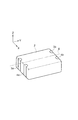
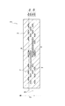
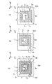
図1は、本実施形態に係る積層型電子部品を示す斜視図であり、図2は、図1に示す積層型電子部品をII線でコイル軸方向Zに切断した断面を示す図である。なお、本実施形態における積層型電子部品1は、本発明をコモンモードチョークコイルに適用したものである。積層型電子部品1は、絶縁材料によって形成された直方体形状の本体部2と、この本体部2の内部に形成されコイル軸方向Zに並列する2つのコイル部5a,5bと、本体部2の長手方向の一組の端面に形成された2対の外部電極3a,3b,4a,4bとを備えている。この外部電極3a,3b,4a,4bは、例えば、銀を主成分とする図示しない端子電極と、この端子電極の表面を覆うように形成され、Cu、Ni及びSn等からなる図示しないめっき膜とによって構成されている。このような積層型電子部品1の等価回路図を図3に示す。
FIG. 1 is a perspective view showing a multilayer electronic component according to this embodiment, and FIG. 2 is a diagram showing a cross section of the multilayer electronic component shown in FIG. The multilayer
本体部2は、詳細は後述するが、絶縁性のグリーンシート6がコイル軸方向Zに積層された積層体を焼成することによって形成されている。
Although the details will be described later, the
コイル部5a,5bの各々は、グリーンシート6上に形成された導体パターン7によって構成されている。コイル部5a(5b)は、図2に示す積層型電子部品1において、仮想の平面S上に導体パターン7が矩形状に巻回された巻回部8a(8c)を有している。また、この巻回部8a(8c)には、平面Sと平行に導体パターン7が矩形状に巻回された巻回部8b(8d)がコイル軸方向Zに並列されている。そして、巻回部8a(8c)と巻回部8b(8d)とはスルーホール9を介して電気的に接続されている。
Each of the
なお、積層された導体パターン7付きグリーンシート6の積層方向の少なくとも上部には、導体パターン7が形成されていない1又は複数のグリーンシート6が積層されている。
Note that one or a plurality of
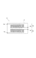
図4は、コイル部5aを構成する導体パターン7が形成されたグリーンシート6を示す図である。同図において、(a)は、巻回部8aを有するグリーンシート6をコイル軸方向Zから見た図であり、(b)は、巻回部8bを有するグリーンシート6をコイル軸方向Zから見た図である。また、図4(c)は、図4(b)に示すグリーンシート6の上に図4(a)に示すグリーンシート6が積層され、巻回部8a,8bがスルーホール9を介して接続されたコイル部5aを示している。
FIG. 4 is a view showing the
グリーンシート6は、上記平面Sに相当する、あるいは平面Sと平行になっている薄板であり、その表面には、導体パターン7が巻回されることによって構成された巻回部8a又は巻回部8bが形成されている。この巻回部8a,8bの巻回方向は、互いが接続されたとき、コイル部5aが同一方向に巻回されたものとなるようになっている。
The
導体パターン7の一方の端部7a,7bは、グリーンシート6の縁部まで引き出されており、それぞれ外部電極3a,3b又は4a,4bに接続されている。そして、巻回部8a,8bは、図4(c)に示すように、巻回部8bの上に巻回部8aが配置された際、導体パターン7の他方の端部7c,7dが、グリーンシート6を貫通するスルーホールを介して接続される。
One
そして、巻回部8a,8bは、導体パターン7の巻回の間隔が互いに等しい部分を有しており、この部分は、図4(c)に示すように、巻回部8aと巻回部8bとがコイル軸方向Zに並列して接続されたとき、スルーホール9を挟んだ両側に位置し、平面Sと平行な方向にずれた状態となっている。ここでいう「巻回の間隔」とは、巻回された導体パターン7において、ある領域とその外側に巻回されている領域との間隔のことである(例えば、図4(a),(b)に示す間隔D)。
The winding
これをより具体的に説明すると、本実施形態に係る巻回部8a,8bは矩形状に巻回されているため、一方向(ここではX方向)に延びる直線状のライン部L1と、このライン部L1に直交する方向(ここではY方向)に延びる直線状のライン部L2とをそれぞれ有している。そして、巻回部8a,8bのライン部L1,L1同士及びライン部L2,L2同士が、平面Sと平行な方向にずれた状態となる(図4(c)参照)。そのため、本体部2をコイル軸方向Zに沿った断面で見ると、図2に示すように、導体パターン7は千鳥状に配置されている。
To explain this more specifically, the
図5は、コイル部5bを構成する導体パターン7が形成されたグリーンシート6を示す図である。同図において、(a)は、巻回部8cを有するグリーンシート6をコイル軸方向Zから見た図であり、(b)は、巻回部8dを有するグリーンシート6をコイル軸方向Zから見た図である。また、図5(c)は、図5(b)に示すグリーンシート6の上に図5(a)に示すグリーンシート6が積層され、巻回部8c,8dがスルーホール9を介して接続されたコイル部5bを示している。
FIG. 5 is a view showing the
図5(c)に示すコイル部5bにおいても上記コイル部5aと同様に、巻回部8c,8dが、導体パターン7の巻回の間隔が互いに等しい部分を有していると共に、この部分が、図5(c)に示すように、巻回部8cと巻回部8dとがコイル軸方向Zに並列して接続されたとき、平面Sと平行な方向にずれた状態となっている。つまり、矩形状に巻回された巻回部8c,8dにおいて、一方向に延びる直線状のライン部L1,L1同士及びこのライン部L1,L1に直交する方向に延びる直線状のライン部L2,L2同士が、平面Sと平行な方向にずれた状態となっている(図5(c)参照)。そのため、本体部2をコイル軸方向Zに沿った断面で見ると、図2に示すように、導体パターン7は千鳥状に配置されている。
Also in the
また、コイル部5a及びコイル部5bにおける隣り合った巻回部8b,8cも、互いのライン部L1,L1同士及びライン部L2,L2同士が平面Sと平行な方向にずれた状態となっている。このため、本体部2をコイル軸方向Zに沿った断面で見ると、図2に示すように、巻回部8a〜8dを通して導体パターン7が千鳥状に配置された状態となっている。
Further, the adjacent winding
図5(c)に示すコイル部5bを構成するグリーンシート6,6の上には、図4(c)に示すコイル部5bを構成するグリーンシート6,6が積層される。その後、後述する、圧着、切断、焼成、外部電極形成等の工程を経ることにより、図1に示す積層型電子部品1が得られる。
以下、上記積層型電子部品1の製造方法について説明する。
Hereinafter, a method for manufacturing the multilayer
まず、Ni−Cu−Zn系フェライト、Ni−Cu−Zn−Mg系フェライト、Cu−Zn系フェライト、Ni−Cu系フェライト等の磁性体を用いて得られるスラリーを、ドクターブレード法等によりベースフィルム上に所定の厚みで塗布して切断し、複数枚の磁性体のグリーンシート(絶縁体層)6を作製する。なお、後述する積層型電子部品30,40では、その一部に非磁性体のグリーンシート6が用いられている。このような非磁性体のグリーンシートを作製する場合は、Fe2O3,ZnO,CuOの混合物を原料としたスラリーをドクターブレード法等によりベースフィルム上に塗布して切断する。そして、グリーンシート6の所定の位置に、レーザー加工等によってスルーホール9を形成する。
First, a slurry obtained by using a magnetic material such as Ni—Cu—Zn ferrite, Ni—Cu—Zn—Mg ferrite, Cu—Zn ferrite, Ni—Cu ferrite, etc. is formed into a base film by a doctor blade method or the like. A plurality of magnetic green sheets (insulator layers) 6 are produced by applying and cutting the film to a predetermined thickness. Note that a non-magnetic
次に、Agを主成分とした導体ペーストを用いて、例えばスクリーン印刷により、グリーンシート6上に導体パターン7を形成し、その後乾燥させる。このとき、上記巻回部8a〜8dがそれぞれ一枚のグリーンシート6の表面に設けられるように導体パターン7を形成する。
Next, a
次に、グリーンシート6と、導体パターン7付きグリーンシート6とを積層・圧着する。この場合、4枚の導体パターン7付きグリーンシート6を積層し、その導体パターン7付きグリーンシート6の上に1又は複数のグリーンシート6を積層する。これにより、グリーンシート6上の導体パターン7が保護される。なお、1又は複数のグリーンシート6を積層し、その上に4枚の導体パターン7付きグリーンシート6を積層するようにしてもよい。また、圧着の際に加える圧力は、例えば、65〜100MPa程度とするのが好ましい。
Next, the
グリーンシート6のスルーホール9は、コイル軸方向Zに隣り合う巻回部8a,8b及び巻回部8c,8dの導体パターン7の端部同士が重なる部位に形成されており、巻回部8a,8bの導体パターン7及び巻回部8c,8dの導体パターン7がグリーンシート6の積層によりスルーホール9を介してそれぞれ接続されるようになっている。
The through
通常、グリーンシート6が積層された段階では、コイル軸方向Zに並列したコイル部の組がコイル軸方向Zと直交する方向に複数配列されたウェハ状となっているため、このウェハを所定の形状・大きさに切断することによって、複数の未焼成状態の本体部2を得る。その後、この未焼成状態の本体部2を所定の温度で焼成して図2に示す本体部2を得る。
Usually, at the stage where the
本体部2は、一般に外部電極3a,3b,4a,4bの形成された位置が特定しやすいように直方体とし、例えば、焼成後に、長手方向(Y方向)の長さが1.2mm、幅方向(X方向)の長さが1.0mm、高さ方向(Z方向)の長さが0.7mm程度(いわゆる1210形状)となるように切断して作製する。この場合、導体パターン7の端部7a,7bが、本体部2の長手方向の端面に位置するように切断する。また、焼成の温度は、例えば、870℃程度とする。
The
次に、導体パターン7の端部7a,7bが露出した本体部2の端面に、銀を主成分とする導体ペーストを塗布した後、700℃度程度で焼き付け、その表面に電気めっきを施して外部電極3a,3b,4a,4bを形成する。なお、電気めっきは、例えば、Cu、NiおよびSn、またはNiおよびSnを用いて行う。以上により、本実施形態に係る積層型電子部品1が完成する。
Next, a conductive paste mainly composed of silver is applied to the end face of the
以上のような積層型電子部品1では、グリーンシート6を積層して圧着する際、導体パターン7からグリーンシート6に加わるコイル軸方向Zの圧力が、平面Sの面方向にほぼ均等になる。このため、グリーンシート6が圧着された後において、グリーンシート6を構成する粒子間の隙間の差が小さくなり、焼成が施された際のデラミネーション及びクラックの発生が抑制される。
In the multilayer
また、コイル部5a及びコイル部5bの隣り合う巻回部8b,8cについても、互いのライン部L1,L1同士及びライン部L2,L2同士が平面Sと平行な方向にずれた状態とすることにより、圧着時にグリーシート6が受けるコイル軸方向Zの圧力の偏りがより低減される。したがって、圧着された後の本体部を構成する粒子間の隙間の差をより小さくすることができる。
The
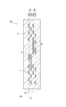
図6は、本発明に係る積層型電子部品の他の形態を示し、コイル軸方向Zに切断した断面を示す図であり、図7は、図6に示す積層型電子部品20のコイル部5a,5bを示す図である。積層型電子部品20は、図7に示すように、スルーホール9が平面Sに平行な方向に互いにずれている点で、上記積層型電子部品1と異なっている。この積層型電子部品20をコイル軸方向Zに沿った断面で見た場合、図6に示すように、スルーホール9が千鳥状に配置されている。
6 shows another embodiment of the multilayer electronic component according to the present invention, and is a diagram showing a cross section cut in the coil axial direction Z. FIG. 7 shows the
このような積層型電子部品20では、グリーンシート6を積層して圧着する際、スルーホール9からグリーンシート6に加わるコイル軸方向Zの圧力も平面Sの面方向に分散される。このため、グリーンシート6を圧着して得られた本体部2を構成する粒子間の隙間の差がさらに小さくなり、焼成が施された際に、スルーホール9付近でデラミネーションやクラックが発生する可能性が低減される。
In such a multilayer
ここで、上記積層型電子部品1,20では本体部2がすべて磁性体から形成されているが、本体部2におけるコイル軸方向Zの上下に非磁性体のグリーンシートから形成された非磁性体部を備えてもよい。以下、非磁性体部を備えた積層型電子部品について説明する。
Here, in the multilayer
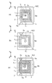
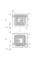
図8、9は、本実施形態に係る積層型電子部品の他の形態を示す図である。図8に示す積層型電子部品30では、本体部2において、本体部2の上面T1及び底面T2のそれぞれから導体パターン7までコイル軸方向Zに沿って連続した領域が磁性体部2a,2aとなっており、それ以外の領域は非磁性体部2bとなっている。つまり、本体部2は、導体パターン7を境に磁性体部2aと非磁性体部2bとに分けられている(図中、境界線を二点鎖線で示す。)。
8 and 9 are diagrams showing another form of the multilayer electronic component according to the present embodiment. In the multilayer
図8に示す積層型電子部品30では、本体部2内の上側に位置するコイル部5aにおいて、上側の巻回部8aを構成する導体パターン7が非磁性体のグリーンシート6に形成され、本体部2内の下側に位置するコイル部5bにおいて、下側の巻回部8dを構成する導体パターン7が磁性体のグリーンシート6に形成され、また、その間の導体パターン7が非磁性体のグリーンシート6に形成されている。これにより、コイル部5aの上側に位置する巻回部8aを構成する導体パターン7を境に、上側が磁性体部2a、下側が非磁性体部2bとなっており、コイル部5bの上側に位置する巻回部8dを構成する導体パターン7を境に、上側が非磁性体部2b、下側が磁性体部2aとなっている。
In the multilayer
上記の積層型電子部品1,20のように本体部2がすべて磁性体で形成された場合は、周波数帯域が1.0(MHz)〜1.0(GHz)程度であるコモンモードノイズを除去できるのに対し、図8に示す積層型電子部品30では、導体パターン間の浮遊容量が低減されるため、10(MHz)〜3.0(GHz)程度の高周波帯域のコモンモードノイズを除去することができる。
When the
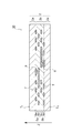
図9に示す積層型電子部品40では、本体部2において、コイル部5a,5bを囲むコイル軸方向Zに沿って連続した領域が非磁性体部2bとなっており、それ以外の領域は磁性体部2aとなっている(図中、境界線を二点鎖線で示す。)。
In the multilayer
図9に示す積層型電子部品40では、本体部2内の上側に位置するコイル部5aにおいて、上側の巻回部8aを構成する導体パターン7の上に非磁性体のグリーンシート6が積層され、本体部2内の下側に位置するコイル部5bにおいて、下側の巻回部8dを構成する導体パターン7が非磁性体のグリーンシート6に形成され、また、その間の導体パターン7が非磁性体のグリーンシート6に形成されている。これにより、巻回部8a〜8dが非磁性体部2b内に形成され、非磁性体部2bの上下には磁性体部2a,2aが形成される。
In the multilayer
このような積層型電子部品40では、導体パターン間の浮遊容量がさらに低減されるため、10(MHz)〜60(GHz)程度の高周波帯域までのコモンモードノイズを除去することができる。
In such a multilayer
以上、本発明の好適な実施形態について詳細に説明したが、本発明は上記実施形態に限定されるものではない。例えば、上記実施形態では、コイル部5a,5bの両方において、互いの導体パターン7がずれた状態となっているが、コイル部5a,5bのいずれか一方がずれた状態であってもよい。また、本発明は、コイル部5a,5bのいずれか一方にコンデンサ回路を付加することによって構成されたLCフィルタにも適用することができる。
The preferred embodiment of the present invention has been described in detail above, but the present invention is not limited to the above embodiment. For example, in the above embodiment, the
以下、実施例及び比較例を挙げ、本発明の積層型電子部品の内容をさらに詳しく説明するが、本発明はこれらの実施例に何ら限定されるものではない。 Hereinafter, although an Example and a comparative example are given and the content of the multilayer electronic component of this invention is demonstrated in detail, this invention is not limited to these Examples at all.
実施例として、本発明に係る積層型電子部品を用い、比較例として、巻回部における導体パターンの大部分がコイル軸方向に重なり合っている従来の積層型電子部品を用いて、それぞれのデラミネーション及びクラックの発生数を調べた。 As an example, the multilayer electronic component according to the present invention is used, and as a comparative example, a conventional multilayer electronic component in which most of the conductor pattern in the winding portion overlaps in the coil axis direction is used. And the number of occurrence of cracks was examined.
実施例及び比較例に係る積層型電子部品は、上述した製造方法において、非磁性体のグリーンシートの厚みを18μmとし、磁性体のグリーンシートの厚みを20μmとなるようにした。また、焼成後の導体パターンは、幅50μm、厚み14μmとなるようにし、導体パターンの巻回の間隔(図4における間隔D)は80μmとなるようにした。 In the multilayer electronic components according to Examples and Comparative Examples, the thickness of the non-magnetic green sheet was set to 18 μm and the thickness of the magnetic green sheet was set to 20 μm in the manufacturing method described above. Moreover, the conductor pattern after firing was made to have a width of 50 μm and a thickness of 14 μm, and the winding interval (interval D in FIG. 4) of the conductor pattern was set to 80 μm.
このような実施例及び比較例に係る積層型電子部品をそれぞれ約60000(個/ロッド)製造し、その中から抜き取り検査を行ってデラミネーション及びクラックの発生状況を調べた。まず、それぞれ600個の抜き取り検査を行ってクラックの発生数を調べたところ、比較例に係る積層型電子部品の発生率が0.5%であったのに対し、実施例に係る積層型電子部品の発生率は0%であった。また、60個を抜き取り、断面検査を行った結果、ショートに至る可能性があるデラミネーションが生じていたものが、比較例に係る積層型電子部品では3個確認されたが、実施例に係る積層型電子部品では0個であった。 About 60000 (pieces / rod) of each of the multilayer electronic components according to the examples and the comparative examples were manufactured, and a sampling inspection was performed from among them to examine the occurrence of delamination and cracks. First, 600 samples were sampled and the number of occurrences of cracks was examined. The occurrence rate of the multilayer electronic component according to the comparative example was 0.5%, whereas the multilayer electronic component according to the example was The incidence of parts was 0%. In addition, as a result of extracting 60 pieces and performing a cross-sectional inspection, it was confirmed that there were three delaminations that could lead to a short circuit in the multilayer electronic component according to the comparative example. The number of multilayer electronic components was zero.
以上により、本発明に係る積層型電子部品は、デラミネーション及びクラックの発生を確実に抑制することができるため信頼性が高く、量産性にも優れたものであることが確認された。 From the above, it was confirmed that the multilayer electronic component according to the present invention can reliably suppress the occurrence of delamination and cracks, and thus has high reliability and excellent mass productivity.
1…積層型電子部品、2…本体部、2a…磁性体部、2b…非磁性体部、5a,5b…コイル部、7…導体パターン、8a〜8d…巻回部、9…スルーホール、20,30,40…積層型電子部品、L1,L2…ライン部、S…平面(仮想の平面)、Z…コイル軸方向。
DESCRIPTION OF
Claims (12)
前記本体部内に形成され、コイル軸方向に並列された第1及び第2のコイル部とを備え、
前記第1及び第2のコイル部の各々は、導体パターンが仮想の平面上に巻回された第1の巻回部と、前記平面と平行に導体パターンが巻回され前記コイル軸方向に前記第1の巻回部と並列されると共に、前記第1の巻回部とスルーホールを介して電気的に接続された第2の巻回部とを有し、
前記第1及び第2のコイル部の少なくとも一方において、前記第1及び第2の巻回部は、前記導体パターンの巻回の間隔が互いに等しい部分を有し、この部分は前記平面と平行な方向にずれていることを特徴とする積層型電子部品。 A main body formed of an insulating material;
The first and second coil portions formed in the main body portion and arranged in parallel in the coil axis direction,
Each of the first and second coil portions includes a first winding portion in which a conductor pattern is wound on an imaginary plane, and a conductor pattern wound in parallel to the plane so that the coil axis direction is A second winding part that is parallel to the first winding part and electrically connected to the first winding part through a through hole;
In at least one of the first and second coil portions, the first and second winding portions have a portion in which the winding interval of the conductor pattern is equal to each other, and this portion is parallel to the plane. A multilayer electronic component characterized by being displaced in a direction.
前記本体部内に形成され、コイル軸方向に並列された第1及び第2のコイル部とを備え、
前記第1及び第2のコイル部の各々は、導体パターンが仮想の平面上に矩形状に巻回された第1の巻回部と、前記平面と平行に導体パターンが矩形状に巻回され前記コイル軸方向に前記第1の巻回部と並列されると共に、前記第1の巻回部とスルーホールを介して電気的に接続された第2の巻回部とを有し、
前記第1及び第2の巻回部は、一方向に延びる直線状の第1ライン部と、前記第1ライン部に略直交する方向に延びる直線状の第2ライン部とを有し、
前記第1及び第2のコイル部の少なくとも一方において、前記第1及び第2の巻回部の前記第1ライン部同士及び第2ライン部同士が互いに前記平面と平行な方向にずれていることを特徴とする積層型電子部品。 A main body formed of an insulating material;
The first and second coil portions formed in the main body portion and arranged in parallel in the coil axis direction,
Each of the first and second coil portions includes a first winding portion in which a conductor pattern is wound in a rectangular shape on a virtual plane, and a conductor pattern wound in a rectangular shape in parallel with the plane. A second winding portion that is arranged in parallel with the first winding portion in the coil axis direction and electrically connected to the first winding portion through a through hole;
The first and second winding parts include a linear first line part extending in one direction and a linear second line part extending in a direction substantially orthogonal to the first line part,
In at least one of the first and second coil portions, the first line portions and the second line portions of the first and second winding portions are displaced from each other in a direction parallel to the plane. A multilayer electronic component characterized by
前記本体部内に形成され、コイル軸方向に並列された第1及び第2のコイル部とを備え、
前記第1及び第2のコイル部の各々は、導体パターンが仮想の平面上に巻回された第1の巻回部と、前記平面と平行に導体パターンが巻回され前記コイル軸方向に前記第1の巻回部と並列されると共に、前記第1の巻回部とスルーホールを介して電気的に接続された第2の巻回部とを有し、
前記第1及び第2のコイル部の少なくとも一方における前記導体パターンは、前記本体部の前記コイル軸方向に沿った断面において千鳥状に配置されていることを特徴とする積層型電子部品。 A main body formed of an insulating material;
The first and second coil portions formed in the main body portion and arranged in parallel in the coil axis direction,
Each of the first and second coil portions includes a first winding portion in which a conductor pattern is wound on an imaginary plane, and a conductor pattern wound in parallel to the plane so that the coil axis direction is A second winding part that is parallel to the first winding part and electrically connected to the first winding part through a through hole;
The multilayer electronic component, wherein the conductor patterns in at least one of the first and second coil portions are arranged in a staggered manner in a cross section along the coil axis direction of the main body portion.
Priority Applications (1)
| Application Number | Priority Date | Filing Date | Title |
|---|---|---|---|
| JP2004106689A JP2005294486A (en) | 2004-03-31 | 2004-03-31 | Laminated electronic component |
Applications Claiming Priority (1)
| Application Number | Priority Date | Filing Date | Title |
|---|---|---|---|
| JP2004106689A JP2005294486A (en) | 2004-03-31 | 2004-03-31 | Laminated electronic component |
Publications (1)
| Publication Number | Publication Date |
|---|---|
| JP2005294486A true JP2005294486A (en) | 2005-10-20 |
Family
ID=35327087
Family Applications (1)
| Application Number | Title | Priority Date | Filing Date |
|---|---|---|---|
| JP2004106689A Pending JP2005294486A (en) | 2004-03-31 | 2004-03-31 | Laminated electronic component |
Country Status (1)
| Country | Link |
|---|---|
| JP (1) | JP2005294486A (en) |
Cited By (14)
| Publication number | Priority date | Publication date | Assignee | Title |
|---|---|---|---|---|
| JP2007123726A (en) * | 2005-10-31 | 2007-05-17 | Tdk Corp | Laminated electronic component |
| WO2012086397A1 (en) * | 2010-12-21 | 2012-06-28 | 株式会社村田製作所 | Laminated coil component |
| WO2012111204A1 (en) * | 2011-02-15 | 2012-08-23 | 株式会社村田製作所 | Layered electronic component |
| JP2013115242A (en) * | 2011-11-29 | 2013-06-10 | Kyocera Corp | Substrate with built-in coil and electronic device |
| KR101490650B1 (en) | 2013-03-01 | 2015-02-05 | 가부시키가이샤 무라타 세이사쿠쇼 | Laminated coil and manufacturing method thereof |
| JP2015142136A (en) * | 2014-01-29 | 2015-08-03 | イノチップ テクノロジー シーオー エルティディー | Laminate chip element |
| US9312062B2 (en) | 2012-03-16 | 2016-04-12 | Murata Manufacturing Co., Ltd. | Common mode choke coil |
| JP2016178255A (en) * | 2015-03-20 | 2016-10-06 | 株式会社リコー | Transformer and plasma generator |
| JP2018056513A (en) * | 2016-09-30 | 2018-04-05 | 株式会社村田製作所 | Electronic component |
| JP2019161092A (en) * | 2018-03-15 | 2019-09-19 | パナソニックIpマネジメント株式会社 | Common mode noise filter |
| KR20200061278A (en) * | 2018-11-23 | 2020-06-02 | 한국전자통신연구원 | Stacked Inductor |
| WO2020121592A1 (en) * | 2018-12-10 | 2020-06-18 | 株式会社村田製作所 | Coil component and filter circuit including same |
| US20200265986A1 (en) * | 2019-02-15 | 2020-08-20 | Murata Manufacturing Co., Ltd. | Inductor component |
| WO2025070097A1 (en) * | 2023-09-27 | 2025-04-03 | パナソニックIpマネジメント株式会社 | Common mode noise filter |
Citations (7)
| Publication number | Priority date | Publication date | Assignee | Title |
|---|---|---|---|---|
| JPS59151411U (en) * | 1983-03-30 | 1984-10-11 | 東芝ライテック株式会社 | High frequency printed coil transformer |
| JPH04206905A (en) * | 1990-11-30 | 1992-07-28 | Murata Mfg Co Ltd | Laminated transformer |
| JPH05243048A (en) * | 1992-02-28 | 1993-09-21 | Fuji Electric Co Ltd | Thin film magnetic element |
| JPH08130117A (en) * | 1994-10-31 | 1996-05-21 | Kyocera Corp | Multilayer inductor |
| JPH09180939A (en) * | 1995-12-22 | 1997-07-11 | Murata Mfg Co Ltd | Multilayer coil part |
| WO2001067470A1 (en) * | 2000-03-08 | 2001-09-13 | Matsushita Electric Industrial Co., Ltd. | Noise filter and electronic device using noise filter |
| JP2002190410A (en) * | 2000-12-22 | 2002-07-05 | Tdk Corp | Laminated transformer |
-
2004
- 2004-03-31 JP JP2004106689A patent/JP2005294486A/en active Pending
Patent Citations (7)
| Publication number | Priority date | Publication date | Assignee | Title |
|---|---|---|---|---|
| JPS59151411U (en) * | 1983-03-30 | 1984-10-11 | 東芝ライテック株式会社 | High frequency printed coil transformer |
| JPH04206905A (en) * | 1990-11-30 | 1992-07-28 | Murata Mfg Co Ltd | Laminated transformer |
| JPH05243048A (en) * | 1992-02-28 | 1993-09-21 | Fuji Electric Co Ltd | Thin film magnetic element |
| JPH08130117A (en) * | 1994-10-31 | 1996-05-21 | Kyocera Corp | Multilayer inductor |
| JPH09180939A (en) * | 1995-12-22 | 1997-07-11 | Murata Mfg Co Ltd | Multilayer coil part |
| WO2001067470A1 (en) * | 2000-03-08 | 2001-09-13 | Matsushita Electric Industrial Co., Ltd. | Noise filter and electronic device using noise filter |
| JP2002190410A (en) * | 2000-12-22 | 2002-07-05 | Tdk Corp | Laminated transformer |
Cited By (22)
| Publication number | Priority date | Publication date | Assignee | Title |
|---|---|---|---|---|
| JP2007123726A (en) * | 2005-10-31 | 2007-05-17 | Tdk Corp | Laminated electronic component |
| WO2012086397A1 (en) * | 2010-12-21 | 2012-06-28 | 株式会社村田製作所 | Laminated coil component |
| WO2012111204A1 (en) * | 2011-02-15 | 2012-08-23 | 株式会社村田製作所 | Layered electronic component |
| JP2013115242A (en) * | 2011-11-29 | 2013-06-10 | Kyocera Corp | Substrate with built-in coil and electronic device |
| US9312062B2 (en) | 2012-03-16 | 2016-04-12 | Murata Manufacturing Co., Ltd. | Common mode choke coil |
| KR101490650B1 (en) | 2013-03-01 | 2015-02-05 | 가부시키가이샤 무라타 세이사쿠쇼 | Laminated coil and manufacturing method thereof |
| US9349534B2 (en) | 2013-03-01 | 2016-05-24 | Murata Manufacturing Co., Ltd. | Multilayer coil and a manufacturing method thereof |
| JP2015142136A (en) * | 2014-01-29 | 2015-08-03 | イノチップ テクノロジー シーオー エルティディー | Laminate chip element |
| US9431988B2 (en) | 2014-01-29 | 2016-08-30 | Innochips Technology Co., Ltd. | Stacked chip device |
| JP2016178255A (en) * | 2015-03-20 | 2016-10-06 | 株式会社リコー | Transformer and plasma generator |
| JP2018056513A (en) * | 2016-09-30 | 2018-04-05 | 株式会社村田製作所 | Electronic component |
| JP2019161092A (en) * | 2018-03-15 | 2019-09-19 | パナソニックIpマネジメント株式会社 | Common mode noise filter |
| JP7126042B2 (en) | 2018-03-15 | 2022-08-26 | パナソニックIpマネジメント株式会社 | common mode noise filter |
| KR20200061278A (en) * | 2018-11-23 | 2020-06-02 | 한국전자통신연구원 | Stacked Inductor |
| KR102390492B1 (en) * | 2018-11-23 | 2022-04-26 | 한국전자통신연구원 | Stacked Inductor |
| WO2020121592A1 (en) * | 2018-12-10 | 2020-06-18 | 株式会社村田製作所 | Coil component and filter circuit including same |
| JP6733856B1 (en) * | 2018-12-10 | 2020-08-05 | 株式会社村田製作所 | Coil component and filter circuit including the same |
| US20200265986A1 (en) * | 2019-02-15 | 2020-08-20 | Murata Manufacturing Co., Ltd. | Inductor component |
| US11837395B2 (en) * | 2019-02-15 | 2023-12-05 | Murata Manufacturing Co., Ltd. | Inductor component |
| US20240055174A1 (en) * | 2019-02-15 | 2024-02-15 | Murata Manufacturing Co., Ltd. | Inductor component |
| US12412694B2 (en) * | 2019-02-15 | 2025-09-09 | Murata Manufacturing Co., Ltd. | Inductor component |
| WO2025070097A1 (en) * | 2023-09-27 | 2025-04-03 | パナソニックIpマネジメント株式会社 | Common mode noise filter |
Similar Documents
| Publication | Publication Date | Title |
|---|---|---|
| US7579937B2 (en) | Laminated inductor and method of manufacture of same | |
| CN102771199B (en) | Coil Built-in Substrate | |
| JP5835355B2 (en) | Coil parts | |
| US8466757B2 (en) | Multilayer common mode filter | |
| US11011292B2 (en) | Electronic component | |
| JP5807650B2 (en) | Multilayer coil and manufacturing method thereof | |
| KR20150014390A (en) | Laminated coil | |
| JP2005294486A (en) | Laminated electronic component | |
| CN115394537B (en) | Electronic component and electronic device | |
| JP4780232B2 (en) | Multilayer electronic components | |
| JP2002319519A (en) | Multilayer ceramic electronic component and method of manufacturing the same | |
| JP2018125455A (en) | Laminate coil component | |
| JP4213679B2 (en) | Multilayer inductor | |
| WO2010092861A1 (en) | Electronic component | |
| JP2004153502A (en) | Laminated lc composite component | |
| JP2009176829A (en) | Electronic component | |
| JP4272183B2 (en) | Multilayer electronic components | |
| JP2006173790A (en) | Laminated lc composite component | |
| JP4317179B2 (en) | Multilayer filter | |
| JP2006351954A (en) | Stacked common mode filter | |
| JP2012221994A (en) | Multilayer electronic component | |
| JP2005229219A (en) | Laminated filter and laminated filter array | |
| JP2006013154A (en) | Layered electronic component | |
| JP4960583B2 (en) | Laminated LC composite parts | |
| JP4216856B2 (en) | Multilayer electronic components |
Legal Events
| Date | Code | Title | Description |
|---|---|---|---|
| A621 | Written request for application examination |
Free format text: JAPANESE INTERMEDIATE CODE: A621 Effective date: 20061115 |
|
| A977 | Report on retrieval |
Free format text: JAPANESE INTERMEDIATE CODE: A971007 Effective date: 20080728 |
|
| A131 | Notification of reasons for refusal |
Free format text: JAPANESE INTERMEDIATE CODE: A131 Effective date: 20080805 |
|
| A521 | Written amendment |
Free format text: JAPANESE INTERMEDIATE CODE: A523 Effective date: 20081006 |
|
| A02 | Decision of refusal |
Free format text: JAPANESE INTERMEDIATE CODE: A02 Effective date: 20081104 |