JP2005292331A - 液晶表示装置の製造方法 - Google Patents
液晶表示装置の製造方法 Download PDFInfo
- Publication number
- JP2005292331A JP2005292331A JP2004105222A JP2004105222A JP2005292331A JP 2005292331 A JP2005292331 A JP 2005292331A JP 2004105222 A JP2004105222 A JP 2004105222A JP 2004105222 A JP2004105222 A JP 2004105222A JP 2005292331 A JP2005292331 A JP 2005292331A
- Authority
- JP
- Japan
- Prior art keywords
- film
- tft
- source
- liquid crystal
- display device
- Prior art date
- Legal status (The legal status is an assumption and is not a legal conclusion. Google has not performed a legal analysis and makes no representation as to the accuracy of the status listed.)
- Granted
Links
Images


Classifications
-
- B—PERFORMING OPERATIONS; TRANSPORTING
- B62—LAND VEHICLES FOR TRAVELLING OTHERWISE THAN ON RAILS
- B62D—MOTOR VEHICLES; TRAILERS
- B62D65/00—Designing, manufacturing, e.g. assembling, facilitating disassembly, or structurally modifying motor vehicles or trailers, not otherwise provided for
- B62D65/02—Joining sub-units or components to, or positioning sub-units or components with respect to, body shell or other sub-units or components
- B62D65/06—Joining sub-units or components to, or positioning sub-units or components with respect to, body shell or other sub-units or components the sub-units or components being doors, windows, openable roofs, lids, bonnets, or weather strips or seals therefor
-
- G—PHYSICS
- G02—OPTICS
- G02F—OPTICAL DEVICES OR ARRANGEMENTS FOR THE CONTROL OF LIGHT BY MODIFICATION OF THE OPTICAL PROPERTIES OF THE MEDIA OF THE ELEMENTS INVOLVED THEREIN; NON-LINEAR OPTICS; FREQUENCY-CHANGING OF LIGHT; OPTICAL LOGIC ELEMENTS; OPTICAL ANALOGUE/DIGITAL CONVERTERS
- G02F1/00—Devices or arrangements for the control of the intensity, colour, phase, polarisation or direction of light arriving from an independent light source, e.g. switching, gating or modulating; Non-linear optics
- G02F1/01—Devices or arrangements for the control of the intensity, colour, phase, polarisation or direction of light arriving from an independent light source, e.g. switching, gating or modulating; Non-linear optics for the control of the intensity, phase, polarisation or colour
- G02F1/13—Devices or arrangements for the control of the intensity, colour, phase, polarisation or direction of light arriving from an independent light source, e.g. switching, gating or modulating; Non-linear optics for the control of the intensity, phase, polarisation or colour based on liquid crystals, e.g. single liquid crystal display cells
- G02F1/133—Constructional arrangements; Operation of liquid crystal cells; Circuit arrangements
- G02F1/1333—Constructional arrangements; Manufacturing methods
- G02F1/1345—Conductors connecting electrodes to cell terminals
- G02F1/13454—Drivers integrated on the active matrix substrate
-
- H—ELECTRICITY
- H10—SEMICONDUCTOR DEVICES; ELECTRIC SOLID-STATE DEVICES NOT OTHERWISE PROVIDED FOR
- H10D—INORGANIC ELECTRIC SEMICONDUCTOR DEVICES
- H10D86/00—Integrated devices formed in or on insulating or conducting substrates, e.g. formed in silicon-on-insulator [SOI] substrates or on stainless steel or glass substrates
- H10D86/01—Manufacture or treatment
- H10D86/021—Manufacture or treatment of multiple TFTs
- H10D86/0231—Manufacture or treatment of multiple TFTs using masks, e.g. half-tone masks
Landscapes
- Physics & Mathematics (AREA)
- Nonlinear Science (AREA)
- Engineering & Computer Science (AREA)
- Chemical & Material Sciences (AREA)
- Optics & Photonics (AREA)
- Mathematical Physics (AREA)
- Crystallography & Structural Chemistry (AREA)
- General Physics & Mathematics (AREA)
- Liquid Crystal (AREA)
- Mechanical Engineering (AREA)
- Manufacturing & Machinery (AREA)
- Transportation (AREA)
- Combustion & Propulsion (AREA)
- Thin Film Transistor (AREA)
- Devices For Indicating Variable Information By Combining Individual Elements (AREA)
Abstract
【解決手段】マトリクス状に形成された多数の画素領域を薄膜トランジスタ(TFT)により駆動して画像情報を表示する液晶表示装置を製造する際、表示部のTFTおよび周辺部の保護用TFTを、同一サイズ(外形寸法)のTFTにより形成する。
【選択図】図1
Description
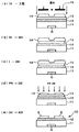
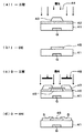
表示部のTFTおよび周辺部の保護用TFTを、同一サイズ(外形寸法)のTFTにより形成する液晶表示装置の製造方法。
前記ガラス基板の他面のゲート電極上にゲート絶縁膜としてSiN膜およびチャネル活性層としてa−Si膜を形成する工程と、
ソース・ドレイン電極との接続のためのn+−a−Si膜を、CVD法を使用して連続成膜を行って形成する工程と、
前記n+−a−Si膜上に、スパッタ法を用いて、ソース・ドレイン電極を堆積する工程と、
レジストを塗布後に前記ソース・ドレイン電極を、グレイトーンマスクを用いて、完全に露光された領域(TFT領域およびソースのバスライン外)、一部露光された領域(ソース・ドレイン電極間のチャネル部領域CH)および完全に露光されない領域(ソース・ドレイン電極部およびソースのバスライン領域)を形成する工程と、
前記レジストパターンをマスクとして、ゲート絶縁膜であるSiN膜をストッパとし、ドライエッチングにより、ソース・ドレイン電極膜、ソースのバスライン、n+−a−Si膜およびa−Si膜をエッチングし、チャネル部に露光マスクに限界解像力以上のスリットパターンを配した保護トランジスタで、レジストが完全に除去された部分のn+−a−Si膜およびa−Si膜までエッチングして、トランジスタの実効Wを小さくした後、前記チャネル部上のレジスト膜を除去するためのアッシングを行う工程と、
レジストパターンを用いてドライエッチングし、ソース・ドレイン電極およびn+−a−Si膜までエッチングを行い、チャンネル活性層をストッパとしてチャネル領域を形成する工程と、
レジストを剥離することにより、外形が同一で実効W/Lが異なるTFTを形成する工程と、
を備えて成る液晶表示装置の製造方法。
11 ガラス基板
14 レジスト
15 フォトマスク
G ゲート電極
S ソース電極
D ドレイン電極
Claims (3)
- マトリクス状に形成された多数の画素領域を薄膜トランジスタ(TFT)により駆動して画像情報を表示する液晶表示装置において、
表示部のTFTおよび周辺部の保護用TFTを、同一サイズ(外形寸法)のTFTにより形成することを特徴とする液晶表示装置の製造方法。 - 前記表示部のTFTおよび前記周辺部の保護用TFTは、チャネル部に露光機の限界解像力以下の寸法のパターンが形成されたグレイトーンマスクを使用して製造することを特徴とする請求項1に記載の液晶表示装置の製造方法。
- ガラス基板の一面にスパッタによりゲート電極を堆積し、フォトリソグラフィ法で前記ゲート電極のパターン形成した後にエッチングを行って所望のゲート電極を形成する工程と、
前記ガラス基板の他面のゲート電極上にゲート絶縁膜としてSiN膜およびチャネル活性層としてa−Si膜を形成する工程と、
ソース・ドレイン電極との接続のためのn+−a−Si膜を、CVD法を使用して連続成膜を行って形成する工程と、
前記n+−a−Si膜上に、スパッタ法を用いて、ソース・ドレイン電極を堆積する工程と、
レジストを塗布後に前記ソース・ドレイン電極を、グレイトーンマスクを用いて、完全に露光された領域(TFT領域およびソースのバスライン外)、一部露光された領域(ソース・ドレイン電極間のチャネル部領域CH)および完全に露光されない領域(ソース・ドレイン電極部およびソースのバスライン領域)を形成する工程と、
前記レジストパターンをマスクとして、ゲート絶縁膜であるSiN膜をストッパとし、ドライエッチングにより、ソース・ドレイン電極膜、ソースのバスライン、n+−a−Si膜およびa−Si膜をエッチングし、チャネル部に露光マスクに限界解像力以上のスリットパターンを配した保護トランジスタで、レジストが完全に除去された部分のn+−a−Si膜およびa−Si膜までエッチングして、トランジスタの実効Wを小さくした後、前記チャネル部上のレジスト膜を除去するためのアッシングを行う工程と、
レジストパターンを用いてドライエッチングし、ソース・ドレイン電極およびn+−a−Si膜までエッチングを行い、チャンネル活性層をストッパとしてチャネル領域を形成する工程と、
レジストを剥離することにより、外形が同一で実効W/Lが異なるTFTを形成する工程と、
を備えて成ることを特徴とする液晶表示装置の製造方法。
Priority Applications (5)
| Application Number | Priority Date | Filing Date | Title |
|---|---|---|---|
| JP2004105222A JP4480442B2 (ja) | 2004-03-31 | 2004-03-31 | 液晶表示装置の製造方法 |
| TW094109750A TWI311816B (en) | 2004-03-31 | 2005-03-29 | Liquid crystal display panel and manufacturing method thereof |
| US11/092,620 US20050219434A1 (en) | 2004-03-31 | 2005-03-30 | Liquid crystal display panel and manufacturing method thereof |
| KR1020050026373A KR100772267B1 (ko) | 2004-03-31 | 2005-03-30 | 액정 디스플레이 패널 및 그 제조 방법 |
| CNA2005100697401A CN1702529A (zh) | 2004-03-31 | 2005-03-30 | 液晶显示面板及其制造方法 |
Applications Claiming Priority (1)
| Application Number | Priority Date | Filing Date | Title |
|---|---|---|---|
| JP2004105222A JP4480442B2 (ja) | 2004-03-31 | 2004-03-31 | 液晶表示装置の製造方法 |
Publications (2)
| Publication Number | Publication Date |
|---|---|
| JP2005292331A true JP2005292331A (ja) | 2005-10-20 |
| JP4480442B2 JP4480442B2 (ja) | 2010-06-16 |
Family
ID=35053867
Family Applications (1)
| Application Number | Title | Priority Date | Filing Date |
|---|---|---|---|
| JP2004105222A Expired - Lifetime JP4480442B2 (ja) | 2004-03-31 | 2004-03-31 | 液晶表示装置の製造方法 |
Country Status (5)
| Country | Link |
|---|---|
| US (1) | US20050219434A1 (ja) |
| JP (1) | JP4480442B2 (ja) |
| KR (1) | KR100772267B1 (ja) |
| CN (1) | CN1702529A (ja) |
| TW (1) | TWI311816B (ja) |
Cited By (3)
| Publication number | Priority date | Publication date | Assignee | Title |
|---|---|---|---|---|
| JP2009063995A (ja) * | 2007-09-07 | 2009-03-26 | Beijing Boe Optoelectronics Technology Co Ltd | グレースケールマスク |
| JP2009069805A (ja) * | 2007-09-10 | 2009-04-02 | Beijing Boe Optoelectronics Technology Co Ltd | 補償型グレイスケールマスク |
| KR20100045938A (ko) * | 2008-10-24 | 2010-05-04 | 가부시키가이샤 한도오따이 에네루기 켄큐쇼 | 반도체 장치의 제작 방법 |
Families Citing this family (5)
| Publication number | Priority date | Publication date | Assignee | Title |
|---|---|---|---|---|
| TWI300274B (en) * | 2006-04-14 | 2008-08-21 | Wintek Corp | Thin-film transistor array for lcd and the method for manufacturing the same |
| KR101319337B1 (ko) * | 2007-10-23 | 2013-10-16 | 엘지디스플레이 주식회사 | 박막트랜지스터 어레이 기판의 제조방법 |
| CN102945854B (zh) * | 2012-11-13 | 2015-05-13 | 京东方科技集团股份有限公司 | 阵列基板及阵列基板上扇出导线的制作方法、显示装置 |
| FR2998580B1 (fr) * | 2012-11-26 | 2016-10-21 | Institut De Rech Pour Le Developpement Ird | Marqueurs moleculaires et methodes pour l'identification des genotypes de palmier dattier |
| TW201624708A (zh) * | 2014-11-21 | 2016-07-01 | 半導體能源研究所股份有限公司 | 半導體裝置及記憶體裝置 |
Family Cites Families (12)
| Publication number | Priority date | Publication date | Assignee | Title |
|---|---|---|---|---|
| US5589406A (en) * | 1993-07-30 | 1996-12-31 | Ag Technology Co., Ltd. | Method of making TFT display |
| JPH07131030A (ja) * | 1993-11-05 | 1995-05-19 | Sony Corp | 表示用薄膜半導体装置及びその製造方法 |
| US5616935A (en) * | 1994-02-08 | 1997-04-01 | Semiconductor Energy Laboratory Co., Ltd. | Semiconductor integrated circuit having N-channel and P-channel transistors |
| US5539219A (en) * | 1995-05-19 | 1996-07-23 | Ois Optical Imaging Systems, Inc. | Thin film transistor with reduced channel length for liquid crystal displays |
| FR2743658B1 (fr) * | 1996-01-11 | 1998-02-13 | Thomson Lcd | Procede d'adressage d'un ecran plat utilisant une precharge des pixels circuit de commande permettant la mise en oeuvre du procede et son application aux ecrans de grandes dimensions |
| US6587160B2 (en) * | 1997-10-14 | 2003-07-01 | Samsung Electronics Co., Ltd. | Liquid crystal displays |
| KR100292048B1 (ko) * | 1998-06-09 | 2001-07-12 | 구본준, 론 위라하디락사 | 박막트랜지스터액정표시장치의제조방법 |
| US7379039B2 (en) * | 1999-07-14 | 2008-05-27 | Sony Corporation | Current drive circuit and display device using same pixel circuit, and drive method |
| JP4700160B2 (ja) * | 2000-03-13 | 2011-06-15 | 株式会社半導体エネルギー研究所 | 半導体装置 |
| KR100494683B1 (ko) * | 2000-05-31 | 2005-06-13 | 비오이 하이디스 테크놀로지 주식회사 | 4-마스크를 이용한 박막 트랜지스터 액정표시장치의제조시에 사용하는 할프톤 노광 공정용 포토 마스크 |
| JP2002162646A (ja) * | 2000-09-14 | 2002-06-07 | Sony Corp | 反射型液晶表示装置 |
| CN1324540C (zh) * | 2003-06-05 | 2007-07-04 | 三星Sdi株式会社 | 具有多晶硅薄膜晶体管的平板显示装置 |
-
2004
- 2004-03-31 JP JP2004105222A patent/JP4480442B2/ja not_active Expired - Lifetime
-
2005
- 2005-03-29 TW TW094109750A patent/TWI311816B/zh not_active IP Right Cessation
- 2005-03-30 US US11/092,620 patent/US20050219434A1/en not_active Abandoned
- 2005-03-30 CN CNA2005100697401A patent/CN1702529A/zh active Pending
- 2005-03-30 KR KR1020050026373A patent/KR100772267B1/ko not_active Expired - Fee Related
Cited By (4)
| Publication number | Priority date | Publication date | Assignee | Title |
|---|---|---|---|---|
| JP2009063995A (ja) * | 2007-09-07 | 2009-03-26 | Beijing Boe Optoelectronics Technology Co Ltd | グレースケールマスク |
| JP2009069805A (ja) * | 2007-09-10 | 2009-04-02 | Beijing Boe Optoelectronics Technology Co Ltd | 補償型グレイスケールマスク |
| KR20100045938A (ko) * | 2008-10-24 | 2010-05-04 | 가부시키가이샤 한도오따이 에네루기 켄큐쇼 | 반도체 장치의 제작 방법 |
| KR101636305B1 (ko) * | 2008-10-24 | 2016-07-05 | 가부시키가이샤 한도오따이 에네루기 켄큐쇼 | 반도체 장치의 제작 방법 |
Also Published As
| Publication number | Publication date |
|---|---|
| KR20060044987A (ko) | 2006-05-16 |
| KR100772267B1 (ko) | 2007-11-01 |
| CN1702529A (zh) | 2005-11-30 |
| TWI311816B (en) | 2009-07-01 |
| JP4480442B2 (ja) | 2010-06-16 |
| US20050219434A1 (en) | 2005-10-06 |
| TW200601570A (en) | 2006-01-01 |
Similar Documents
| Publication | Publication Date | Title |
|---|---|---|
| US7553707B2 (en) | Method for manufacturing a Liquid crystal display device | |
| US8735888B2 (en) | TFT-LCD array substrate and manufacturing method thereof | |
| US7718994B2 (en) | Array substrates for use in liquid crystal displays and fabrication methods thereof | |
| JP4994014B2 (ja) | フラットパネルディスプレイに使用される薄膜トランジスタの製造方法 | |
| EP3054483A1 (en) | Array substrate, manufacturing method therefor, and display apparatus | |
| US8093110B2 (en) | Method for manufacturing thin film transistor | |
| WO2019100502A1 (zh) | 一种薄膜晶体管液晶显示器阵列基板及其制作方法 | |
| US20120086678A1 (en) | Wire, method of manufacture, and related apparatus | |
| JP6293905B2 (ja) | Tft−lcdアレイ基板の製造方法、液晶パネル、液晶表示装置。 | |
| KR100653467B1 (ko) | 박막 트랜지스터-액정표시소자의 제조방법 | |
| US20070148799A1 (en) | Liquid crystal display and fabrication method thereof | |
| CN100511653C (zh) | 薄膜晶体管及其应用的显示元件的制造方法 | |
| CN100507692C (zh) | 液晶显示器件及其制造方法 | |
| JP4480442B2 (ja) | 液晶表示装置の製造方法 | |
| US6261880B1 (en) | Process for manufacturing thin film transistors | |
| US6184069B1 (en) | Fabrication of thin film transistor-liquid crystal display with self-aligned transparent conducting layers | |
| KR100764273B1 (ko) | 박막트랜지스터 제조방법 | |
| TWI396916B (zh) | 薄膜電晶體陣列基板之製作方法 | |
| CN101330062A (zh) | 薄膜晶体管阵列基板的制作方法 | |
| US20100314634A1 (en) | Pixel structure and manufacturing method thereof and display panel | |
| KR20070045751A (ko) | 포토 마스크 | |
| KR100837884B1 (ko) | 액정표시장치의 제조방법 | |
| KR20020057032A (ko) | 박막트랜지스터 액정표시장치의 제조방법 | |
| KR20070072204A (ko) | 액정표시소자 및 제조방법 | |
| KR980010566A (ko) | 박막트랜지스터 액정 디스플레이 제조 방법 |
Legal Events
| Date | Code | Title | Description |
|---|---|---|---|
| A621 | Written request for application examination |
Free format text: JAPANESE INTERMEDIATE CODE: A621 Effective date: 20070111 |
|
| RD02 | Notification of acceptance of power of attorney |
Free format text: JAPANESE INTERMEDIATE CODE: A7422 Effective date: 20080205 |
|
| A977 | Report on retrieval |
Free format text: JAPANESE INTERMEDIATE CODE: A971007 Effective date: 20091022 |
|
| A131 | Notification of reasons for refusal |
Free format text: JAPANESE INTERMEDIATE CODE: A131 Effective date: 20091127 |
|
| RD02 | Notification of acceptance of power of attorney |
Free format text: JAPANESE INTERMEDIATE CODE: A7422 Effective date: 20091211 |
|
| RD04 | Notification of resignation of power of attorney |
Free format text: JAPANESE INTERMEDIATE CODE: A7424 Effective date: 20091215 |
|
| A521 | Request for written amendment filed |
Free format text: JAPANESE INTERMEDIATE CODE: A523 Effective date: 20100126 |
|
| TRDD | Decision of grant or rejection written | ||
| A01 | Written decision to grant a patent or to grant a registration (utility model) |
Free format text: JAPANESE INTERMEDIATE CODE: A01 Effective date: 20100302 |
|
| A01 | Written decision to grant a patent or to grant a registration (utility model) |
Free format text: JAPANESE INTERMEDIATE CODE: A01 |
|
| A61 | First payment of annual fees (during grant procedure) |
Free format text: JAPANESE INTERMEDIATE CODE: A61 Effective date: 20100316 |
|
| FPAY | Renewal fee payment (event date is renewal date of database) |
Free format text: PAYMENT UNTIL: 20130326 Year of fee payment: 3 |
|
| R150 | Certificate of patent or registration of utility model |
Free format text: JAPANESE INTERMEDIATE CODE: R150 |