JP2005277228A - Transparent electromagnetic wave shield and its use - Google Patents
Transparent electromagnetic wave shield and its use Download PDFInfo
- Publication number
- JP2005277228A JP2005277228A JP2004090692A JP2004090692A JP2005277228A JP 2005277228 A JP2005277228 A JP 2005277228A JP 2004090692 A JP2004090692 A JP 2004090692A JP 2004090692 A JP2004090692 A JP 2004090692A JP 2005277228 A JP2005277228 A JP 2005277228A
- Authority
- JP
- Japan
- Prior art keywords
- transparent
- layer
- electromagnetic wave
- silver
- wave shielding
- Prior art date
- Legal status (The legal status is an assumption and is not a legal conclusion. Google has not performed a legal analysis and makes no representation as to the accuracy of the status listed.)
- Withdrawn
Links
Images

Abstract
Description
本発明は、透明電磁波遮蔽体に関する。さらに詳しくは、銀を含有する薄膜層を有する透明電磁波遮蔽体に関する。 The present invention relates to a transparent electromagnetic wave shielding body. More specifically, the present invention relates to a transparent electromagnetic wave shielding body having a thin film layer containing silver.
近年、電子機器や無線機器の発達が目覚しく、その需要は急増している。電子機器は、電気を用いているため、少なからず電磁波の発生があり、時にはその漏洩電磁波の影響により、他の機器の誤動作を引き起こしたり、また、その電磁波を他人に傍受され、その情報を読み取られる危険性を有している。また、無線機器の場合は、発信される電磁波を傍受され、その電磁波のもつ無線情報を読み取られる危険性がある。また、電磁波朗詠量が多いと健康に影響を及ぼすことを指摘する報告もある。 In recent years, the development of electronic devices and wireless devices has been remarkable, and the demand has been rapidly increasing. Since electronic devices use electricity, there is a considerable amount of electromagnetic waves that are generated, sometimes causing malfunctions of other devices due to the effects of leaked electromagnetic waves, and others can intercept the electromagnetic waves and read the information. There is a risk that In the case of a wireless device, there is a risk that an electromagnetic wave transmitted can be intercepted and wireless information possessed by the electromagnetic wave can be read. There are also reports that point out that a large amount of recitation of electromagnetic waves affects health.
これら電磁波漏洩に伴う、他機器への影響や、情報の漏洩を抑制するために、近年、電磁波遮蔽材料に対する要請が高まっている。電磁波は、金属のような導電性材料で遮蔽することができるが、プラズマディスプレイ(PDP)、各種建築物の窓や自動車窓、半導体部品を保護するための筐体、各種表示機器の表示部分などは、電磁波遮蔽機能に加え、透明性が必要な材料が求められている。このような電磁波遮蔽能と透明性を有する材料としては、大きく二種類に分けることができる。一つは、特開平10−41679号公報(特許文献1)に報告されている様な金属メッシュタイプと呼ばれているものであり、透明基材に細く金属を格子状に配置させたものである。これは、導電性に優れ、優れた電磁波遮蔽能を有するが、モワレ像が生じる問題がある。もう一つは、特公昭59−44993公報(特許文献2)に報告されている様な透明膜タイプと呼ばれるものであり、透明導電性薄膜を透明基体に設けたものである。透明膜タイプの電磁波遮蔽材料は、金属メッシュタイプに比べて、電磁波遮蔽能力に劣るが、モワレ像の発生が無く、視認性、透明性に優れているという特徴がある。 In recent years, there has been an increasing demand for electromagnetic shielding materials in order to suppress the influence on other devices and the leakage of information due to these electromagnetic leakages. Electromagnetic waves can be shielded with a conductive material such as metal, but plasma displays (PDP), windows of various buildings and automobile windows, housings for protecting semiconductor components, display parts of various display devices, etc. In addition to the electromagnetic wave shielding function, a material that requires transparency is required. Such materials having electromagnetic wave shielding ability and transparency can be roughly divided into two types. One is called a metal mesh type as reported in Japanese Patent Application Laid-Open No. 10-41679 (Patent Document 1), in which thin metals are arranged in a lattice pattern on a transparent substrate. is there. Although this is excellent in electroconductivity and has an excellent electromagnetic wave shielding ability, there is a problem that a moire image is generated. The other is called a transparent film type as reported in Japanese Examined Patent Publication No. 59-44993 (Patent Document 2), in which a transparent conductive thin film is provided on a transparent substrate. The transparent film type electromagnetic wave shielding material is inferior to the metal mesh type in electromagnetic wave shielding ability, but has a feature that there is no generation of moire images and excellent visibility and transparency.
透明膜タイプの電磁波遮蔽体の場合、電磁波遮断能力は、当然のことながら、電磁波遮蔽体の面抵抗値が低いほど優れるので、純物質の中で最も比抵抗値が低い銀又は銀を主体とする金属薄膜が上記透明導電薄膜として好適に用いられている。実際には、さらなる透過率上昇及び金属薄膜層の安定性向上の目的で、当該銀を主体とする金属薄膜層を、透明高屈折率薄膜層で挟み込んだ積層体を、透明導電薄膜とするのが通常である。 In the case of a transparent film type electromagnetic wave shielding body, the electromagnetic wave shielding ability is naturally better as the surface resistance value of the electromagnetic wave shielding body is lower. Therefore, silver or silver having the lowest specific resistance value among pure substances is mainly used. A metal thin film is preferably used as the transparent conductive thin film. Actually, for the purpose of further increasing the transmittance and improving the stability of the metal thin film layer, a transparent conductive thin film is formed by sandwiching the metal thin film layer mainly composed of silver with a transparent high refractive index thin film layer. Is normal.
しかしながら、よく知られているように、金属薄膜層材料として好適に用いられる銀は、きわめて原子の凝集を生じやすいという大きな問題がある。銀薄膜層の銀原子が凝集すると、金属薄膜としての低抵抗性が損なわれる他、銀白色の欠点(点状欠陥、又は反射性欠陥、白点とも称される。)を生じる。この銀白色の欠点は、外観上、商品価値を大幅に下落させるとともに、欠点によっては当該金属薄膜材料の有する高透明性や低抵抗性を喪失せしめるものもある。 However, as is well known, silver that is suitably used as a metal thin film layer material has a great problem that it is very likely to cause aggregation of atoms. Aggregation of silver atoms in the silver thin film layer impairs low resistance as a metal thin film, and also causes silver white defects (also referred to as point defects, reflective defects, or white spots). This silver-white defect significantly reduces the commercial value in appearance and, depending on the defect, may cause loss of the high transparency and low resistance of the metal thin film material.
従来、かかる銀薄膜層の銀原子の凝集は、例えば、塩素イオン、硫黄イオンや異物(パーティクル)等の存在下において発生しやすいことが知られており、異物の付着を防止する試みが特開2002−304126公報(特許文献3)で報告されている。一方では、特開2001−57110公報(特許文献4)に記載されている様な金属薄膜層を厚くすることにより、銀の凝集を防止することも試みられている。しかしながら、高い透明性が要求される透明電磁波遮蔽体では、金属薄膜層の厚みに制限があり、上記の方法を適用するには限界がある。他の試みとして、特開2000−329931公報(特許文献5)に記載されている様な銀薄膜層に、銅やプラチナ等の耐蝕性のある金属薄膜を積層する方法もあるが、透明性の低下や面抵抗の上昇を伴う問題がある。 Conventionally, it is known that the aggregation of silver atoms in such a silver thin film layer is likely to occur in the presence of, for example, chlorine ions, sulfur ions, foreign matters (particles), etc. It is reported in 2002-304126 (patent document 3). On the other hand, attempts have been made to prevent the aggregation of silver by increasing the thickness of the metal thin film layer as described in JP 2001-57110 A (Patent Document 4). However, in a transparent electromagnetic wave shield requiring high transparency, the thickness of the metal thin film layer is limited, and there is a limit to applying the above method. As another attempt, there is a method of laminating a corrosion-resistant metal thin film such as copper or platinum on a silver thin film layer as described in JP 2000-329931 A (Patent Document 5). There is a problem with a decrease and an increase in sheet resistance.
これらの対策だけでは銀白色の欠点対策としてだけでも十分とは言えず、銀白色の欠点の発生を容易に抑制できる構成の透明電磁波遮蔽体は、これまで得られていない。このため、歩留まり、生産性等の向上の余地を残しているのが実状である。よって、更に有効な銀白色の欠点を防止する技術開発が、以前にも増して求められている。
従って、本発明の目的は上記の様な銀白色の欠点が、極めて発生の少ない透明電磁波遮蔽体を提供することである。 Accordingly, an object of the present invention is to provide a transparent electromagnetic wave shielding body in which the above-mentioned silver-white defects are extremely rare.
本発明者らはかかる観点から鋭意検討した結果、驚くべきことに、銀含有薄膜を1層以上含む導電層上にハロゲン、硫黄の含有率が50ppm以下の透明な樹脂を直接塗工し、透明樹脂層を形成した積層体が、銀白色欠点の発生の極めて少ない透明電磁波遮蔽体であることを見出し、本発明を完成した。 As a result of intensive studies from such a viewpoint, the present inventors surprisingly applied a transparent resin having a halogen and sulfur content of 50 ppm or less directly on a conductive layer containing one or more silver-containing thin films, and was transparent. The present inventors have found that the laminate formed with the resin layer is a transparent electromagnetic wave shield with very few silver white defects, and completed the present invention.
本発明に従えば、以下の発明が提供される。
すなわち、
(1) 少なくとも銀含有薄膜を1層含む導電層(A)と、
前記導電層(A)上に、塗工法で形成されるハロゲン、硫黄の含有率が50ppm以下の透明な樹脂層(B)とを含み、
A/Bの積層構造を有する透明電磁波遮蔽体が提供される。また、
(2) 好ましくは、少なくとも銀含有薄膜を1層含む導電層(A)が、透明基体層(C)を含む積層構造を有する導電層(A1)であることを特徴とする透明電磁波遮蔽体、
(3) 好ましくは、樹脂層(B)が粘着剤層(B1)であることを特徴とする透明電磁波遮蔽体、
(4) 好ましくは、透明基体層(C)が透明フィルム(C1)であることを特徴とする透明電磁波遮蔽体が提供される。本発明の上記の透明電磁波遮蔽体は、銀白色の欠点の発生が少ない優れた特性を有する。
また、本発明によれば、
(5) 上記の透明電磁波遮蔽体を用いたディスプレイ用フィルターが提供される。本発明の上記のディスプレイ用フィルターは、銀白色の欠点の発生が少なく、且つ、優れた電磁波遮蔽性と透明性とを有している。
また本発明によれば、
(6) 上記の透明電磁波遮蔽体を用いた窓が提供される。本発明の窓は、優れた電磁波遮蔽性と透明性を有しており、またその製造の際の施工性にも優れている。
また本発明によれば、
(7) 上記の透明電磁波遮蔽体を用いた電磁波遮蔽筐体が提供される。本発明の電磁波遮蔽筐体は、長期にわたって優れた電磁波遮蔽性と透明性を示す。
また本発明によれば、
(8) 上記の透明電磁波遮蔽体を用いた表示装置が提供される。本発明の表示装置は、長期にわたって電磁波の発生が少なく、美しい画像を提供することが出来る。
According to the present invention, the following inventions are provided.
That is,
(1) a conductive layer (A) including at least one silver-containing thin film;
On the conductive layer (A), a transparent resin layer (B) having a halogen and sulfur content of 50 ppm or less formed by a coating method,
A transparent electromagnetic wave shielding body having an A / B laminated structure is provided. Also,
(2) Preferably, the transparent electromagnetic wave shielding body, wherein the conductive layer (A) including at least one silver-containing thin film is a conductive layer (A1) having a laminated structure including a transparent substrate layer (C),
(3) Preferably, the transparent electromagnetic wave shielding body, wherein the resin layer (B) is a pressure-sensitive adhesive layer (B1),
(4) Preferably, a transparent electromagnetic wave shielding body characterized in that the transparent substrate layer (C) is a transparent film (C1) is provided. The above-mentioned transparent electromagnetic wave shielding body of the present invention has excellent characteristics with few occurrences of silver-white defects.
Moreover, according to the present invention,
(5) A display filter using the transparent electromagnetic wave shielding body is provided. The above-described display filter of the present invention is less susceptible to silver-white defects and has excellent electromagnetic shielding properties and transparency.
Also according to the invention,
(6) A window using the transparent electromagnetic wave shielding body is provided. The window of the present invention has excellent electromagnetic shielding properties and transparency, and is also excellent in workability during its manufacture.
Also according to the invention,
(7) An electromagnetic wave shielding casing using the transparent electromagnetic wave shielding body is provided. The electromagnetic wave shielding casing of the present invention exhibits excellent electromagnetic wave shielding properties and transparency over a long period of time.
Also according to the invention,
(8) A display device using the transparent electromagnetic wave shielding body is provided. The display device of the present invention can provide beautiful images with little generation of electromagnetic waves over a long period of time.
本発明の透明電磁波遮蔽体は、経時的な銀白色の欠点の発生が極めて少なく出来、且つ、優れた電磁波遮蔽性、透明性、外観を長期にわたって保持出来る。これが、本発明の効果である。このため本発明の工業的意義は大きい。 The transparent electromagnetic wave shielding body of the present invention can generate silver white defects over time and can maintain excellent electromagnetic wave shielding properties, transparency, and appearance over a long period of time. This is the effect of the present invention. For this reason, the industrial significance of the present invention is great.
以下、本発明について詳細に説明する。
本発明の透明電磁波遮蔽体は、銀含有薄膜を1層以上含む導電層(A)と、前記導電層(A)上に塗工法で形成されるハロゲン、硫黄の含有率が50ppm以下の透明な粘着剤層(B)とを含み、A/Bの順の積層構造を有するものである。これらの各構成要素を以下に説明する。
Hereinafter, the present invention will be described in detail.
The transparent electromagnetic wave shielding body of the present invention comprises a conductive layer (A) containing one or more silver-containing thin films, and a transparent content of halogen and sulfur formed on the conductive layer (A) by a coating method with a content of 50 ppm or less. And a pressure-sensitive adhesive layer (B), and has a laminated structure in the order of A / B. Each of these components will be described below.
(少なくとも銀含有薄膜層を一層有する導電層(A))
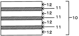
本発明の少なくとも銀含有薄膜層を一層有する導電層(A)は、公知の物を制限無く用いることが出来る。本発明において用いられる、導電層(A)は、銀または銀を含む合金からなる透明金属薄膜層(a1)と透明高屈折率薄膜層(a2)とからなる積層体が好ましいものとして採用される。これは、上記の構成にすることで、透明性、反射特性、導電率などの設計の自由度が高く出来るためである。さらに、後述する銀白色の欠点の発生を抑制しやすい構成であることも理由の一つである。図1は、本発明における少なくとも銀含有薄膜層を一層有する導電層(A)の層構成の一例を示すものである。導電層10は、3層の銀を含む透明導電金属薄膜層11と、4層の透明高屈折率薄膜層12とが、交互に積層された構成を有している。
(Conductive layer (A) having at least one silver-containing thin film layer)
As the conductive layer (A) having at least one silver-containing thin film layer of the present invention, a known material can be used without limitation. As the conductive layer (A) used in the present invention, a laminate comprising a transparent metal thin film layer (a1) made of silver or an alloy containing silver and a transparent high refractive index thin film layer (a2) is preferably used. . This is because the degree of freedom of design such as transparency, reflection characteristics, and conductivity can be increased by using the above-described configuration. Furthermore, it is one of the reasons that it is easy to suppress the occurrence of silver-white defects described later. FIG. 1 shows an example of a layer structure of a conductive layer (A) having at least one silver-containing thin film layer in the present invention. The
透明金属薄膜層(a1)として、銀は、比抵抗が、1.59×10⁻⁶(Ω・cm)と、あらゆる材料の中で最も電気伝導性に優れる上に、薄膜の可視光線透過率が優れるため、最も好適に用いられるのである。一方で、銀は、薄膜とした時に安定性を欠き、硫化や塩素化を受け易いという問題を持っているので、その安定性を向上させるため、銀を含む、すなわち具体的には、銀を主体とする銀合金、例えば、銀と金の合金、銀と銅の合金、銀とパラジウムの合金、銀と銅とパラジウムの合金、銀と白金の合金等を用いる事も出来る。 As the transparent metal thin film layer (a1), silver has a specific resistance of 1.59 × 10 −6 (Ω · cm), which is the most excellent in electrical conductivity among all materials, and the visible light transmittance of the thin film. Therefore, it is most preferably used. On the other hand, silver lacks stability when it is made into a thin film and has the problem of being susceptible to sulfidation and chlorination. Therefore, in order to improve its stability, it contains silver. A silver alloy as a main component, for example, an alloy of silver and gold, an alloy of silver and copper, an alloy of silver and palladium, an alloy of silver, copper and palladium, an alloy of silver and platinum, or the like can also be used.
かかる透明金属薄膜層(a1)の厚さは、本発明の透明電磁波遮蔽体の透過性及び電気伝導性を考慮して決定されるが、通常は、一層につき0.5〜100nm程度である。なお、導電層(A)の最表面が銀を含む透明金属薄膜層(a1)である場合は、その最表面透明金属層における銀の元素組成が、3〜99%(原子割合)であることが好ましい。 透明高屈折率薄膜層(a2)は、公知の物を制限無く用いることが出来る。透明性の高い、例えば、膜厚100nm程度の薄膜を形成したときに、その薄膜の波長400〜700nmの光に対する透過率が60%以上であるような、透明性に優れた材料が好ましく、また、550nmの光に対する屈折率が、1.4以上の材料であるような、高屈折率材料が好ましい。 かかる透明高屈折率薄膜層(a2)用に好適に用いることができる材料としては、例えば、インジウムとスズとの酸化物(ITO)、酸化亜鉛(ZnO)、酸化チタン(TiO2)、カドミウムとスズとの酸化物(CTO)、酸化アルミニウム(Al2O3)、亜鉛とアルミニウムとの酸化物(AZO)、酸化マグネシウム(MgO)、酸化トリウム(ThO2)、酸化スズ(SnO2)、酸化ランタン(LaO2)、酸化珪素(SiO2)、酸化インジウム(In2O3)、酸化ニオブ(Nb2O3)、酸化アンチモン(Sb2O3)、酸化ジルコニウム(ZrO2)、酸化セシウム(CeO2)、酸化ビスマス(BiO2)等が好ましく使用される。また、透明高屈折率硫化物を用いてもよく、具体的に例示すると、硫化亜鉛(ZnS)、硫化カドミウム(CdS)、硫化アンチモン(Sb2S3)等があげられる。透明高屈折率薄膜層(a2)用材料としては、上記の中でもITO、ZnO及びTiO2が特に好ましい。ITO及びZnOは、導電性を持つ上に、可視領域における屈折率が、2.0程度と高く、さらに可視領域にほとんど吸収を持たないためである。TiO2は、絶縁物であり、可視領域にわずかな吸収を持つが、可視光に対する屈折率が2.3程度と大きいことによる。 The thickness of the transparent metal thin film layer (a1) is determined in consideration of the transparency and electrical conductivity of the transparent electromagnetic wave shielding body of the present invention, and is usually about 0.5 to 100 nm per layer. In addition, when the outermost surface of the conductive layer (A) is a transparent metal thin film layer (a1) containing silver, the elemental composition of silver in the outermost surface transparent metal layer is 3 to 99% (atomic ratio). Is preferred. A well-known thing can be used for a transparent high refractive index thin film layer (a2) without a restriction | limiting. A highly transparent material, for example, having a transmittance of 60% or more with respect to light having a wavelength of 400 to 700 nm when a thin film having a thickness of about 100 nm is formed, is preferable. A material having a high refractive index such that the refractive index with respect to light at 550 nm is 1.4 or more is preferable. Examples of materials that can be suitably used for the transparent high refractive index thin film layer (a2) include, for example, oxides of indium and tin (ITO), zinc oxide (ZnO), titanium oxide (TiO 2 ), cadmium, and the like. Oxide with tin (CTO), aluminum oxide (Al 2 O 3 ), oxide with zinc and aluminum (AZO), magnesium oxide (MgO), thorium oxide (ThO 2 ), tin oxide (SnO 2 ), oxidation Lanthanum (LaO 2 ), silicon oxide (SiO 2 ), indium oxide (In 2 O 3 ), niobium oxide (Nb 2 O 3 ), antimony oxide (Sb 2 O 3 ), zirconium oxide (ZrO 2 ), cesium oxide ( CeO 2 ), bismuth oxide (BiO 2 ) and the like are preferably used. A transparent high refractive index sulfide may be used. Specific examples include zinc sulfide (ZnS), cadmium sulfide (CdS), antimony sulfide (Sb 2 S 3 ), and the like. Among the above, ITO, ZnO, and TiO 2 are particularly preferable as the material for the transparent high refractive index thin film layer (a2). This is because ITO and ZnO have electrical conductivity and a refractive index in the visible region is as high as about 2.0, and have almost no absorption in the visible region. TiO 2 is an insulator and has slight absorption in the visible region, but has a large refractive index with respect to visible light of about 2.3.
上記の透明金属薄膜層(a1)と透明高屈折率薄膜層(a2)の多層積層体形成は、スパッタリング法、イオンプレーティング法、真空蒸着法等の従来公知の手法によることができる。なかでもスパッタリング法は、膜厚制御の必要な多層積層構造の形成には好適である。これは、金属薄膜層と高屈折率薄膜層の積層、例えば、銀または銀を含む合金からなる金属薄膜層と主として酸化インジウムで構成される透明高屈折率薄膜層とを容易に繰り返して連続的に成膜、積層できるためである。 Formation of the multilayer laminate of the transparent metal thin film layer (a1) and the transparent high refractive index thin film layer (a2) can be performed by a conventionally known method such as sputtering, ion plating, or vacuum deposition. Among these, the sputtering method is suitable for forming a multilayer laminated structure that requires film thickness control. This is because a metal thin film layer and a high refractive index thin film layer, for example, a metal thin film layer made of silver or an alloy containing silver and a transparent high refractive index thin film layer mainly composed of indium oxide are easily repeated. This is because the film can be formed and laminated.
具体的には、本発明の透明金属薄膜層(a1)の形成には、銀または銀を含む合金をターゲットとし、スパッタガスには、アルゴン等の不活性ガスを用い、通常、圧力0.01〜3.0Pa、直流(DC)あるいは高周波(RF)マグネトロンスパッタリング法を好ましい例として挙げることが出来る。 Specifically, for the formation of the transparent metal thin film layer (a1) of the present invention, silver or an alloy containing silver is used as a target, and an inert gas such as argon is used as a sputtering gas. A preferable example is a -3.0 Pa, direct current (DC) or radio frequency (RF) magnetron sputtering method.
また、透明高屈折率薄膜層(a2)の形成には、例えばインジウムを主成分とする金属ターゲットまたは酸化インジウムを主成分とする焼結体ターゲットを用い、スパッタガスにはアルゴン等の不活性ガスを、反応性ガスには酸素を用い、通常圧力0.01〜3.0Pa、直流(DC)あるいは高周波(RF)マグネトロンスパッタリング法による反応性スパッタリングを適用することができる。 For forming the transparent high refractive index thin film layer (a2), for example, a metal target containing indium as a main component or a sintered body target containing indium oxide as a main component is used, and an inert gas such as argon is used as a sputtering gas. In this case, oxygen is used as a reactive gas, and a reactive sputtering by a normal pressure of 0.01 to 3.0 Pa, direct current (DC) or radio frequency (RF) magnetron sputtering can be applied.
本発明の上記の薄膜厚みや組成の測定方法は、公知の方法を制限無く用いることが出来る。また、その他のより詳細な内容については、例えば特開平10−217380号公報等に記載の内容を採用することが出来る。 As the method for measuring the thickness and composition of the thin film of the present invention, a known method can be used without limitation. For other more detailed contents, for example, the contents described in JP-A-10-217380 can be adopted.
(透明基体層(C))
本発明の導電層(A)は、自立膜として扱うには困難な場合が多いので、本発明においては透明基体層(C)と導電層(A)との積層構造を有する導電層(A1)とすることが好ましい。さらに透明基体層(C)としては、後述する透明フィルム(C1)であることが好ましい。この理由は、導電層(A1)が、ロールトゥーロールプロセスで透明フィルム(C1)上に連続的に導電層(A)を製膜するという生産性の高い製法で製造可能であることによる。
(Transparent substrate layer (C))
Since the conductive layer (A) of the present invention is often difficult to handle as a self-supporting film, in the present invention, the conductive layer (A1) having a laminated structure of the transparent substrate layer (C) and the conductive layer (A). It is preferable that Further, the transparent substrate layer (C) is preferably a transparent film (C1) described later. The reason for this is that the conductive layer (A1) can be manufactured by a highly productive method in which the conductive layer (A) is continuously formed on the transparent film (C1) by a roll-to-roll process.
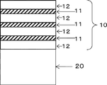
図2に導電層(A1)の一例を示した。図2の様な導電層は、例えば透明基体20上に図1で示したような構成の導電層10をスパッタリング法で形成して得られるものである。
FIG. 2 shows an example of the conductive layer (A1). The conductive layer as shown in FIG. 2 is obtained, for example, by forming the
上記の透明基体層(C)としては、高分子フィルム、樹脂板、ガラス板等を使用することができる。 As the transparent substrate layer (C), a polymer film, a resin plate, a glass plate, or the like can be used.
高分子フィルムとしては、厚み10〜300μm程度の可撓性のある透明性の高い高分子フィルムが好ましく用いられ、例えば、ポリエチレンテレフタレート(PET)、ポリイミド(PI)、ポリスルフォン(PS)、ポリエーテルスルフォン(PES)、ポリメチレンメタクリレート(PMMA)、ポリカーボネート(PC)、ポリエーテルエーテルケトン(PEEK)、ポリプロピレン(PP)、トリアセチルセルロース(TAC)等が挙げられる。中でもポリエチレンテレフタレート(PET)及びトリアセチルセルロース(TAC)が、特に好適に用いられる。 As the polymer film, a flexible and highly transparent polymer film having a thickness of about 10 to 300 μm is preferably used. For example, polyethylene terephthalate (PET), polyimide (PI), polysulfone (PS), polyether Examples include sulfone (PES), polymethylene methacrylate (PMMA), polycarbonate (PC), polyether ether ketone (PEEK), polypropylene (PP), and triacetyl cellulose (TAC). Among these, polyethylene terephthalate (PET) and triacetyl cellulose (TAC) are particularly preferably used.
樹脂板としては、ポリメタクリル酸メチル(PMMA)をはじめとするアクリル樹脂、ポリカーボネート樹脂、透明ABS樹脂等が使用できるが、これらの樹脂に限定されるものではない。樹脂板の厚みは、特に限定されるものではないが、通常1mm〜10mm程度である。 As the resin plate, acrylic resin including polymethyl methacrylate (PMMA), polycarbonate resin, transparent ABS resin and the like can be used, but the resin plate is not limited to these resins. The thickness of the resin plate is not particularly limited, but is usually about 1 mm to 10 mm.
ガラス板を使用する場合は、化学強化加工または風冷強化加工を行った半強化ガラス板または強化ガラス板を用いることが望ましい。重量を考慮すると、その厚みは1〜4mm程度である事が好ましい。 When a glass plate is used, it is desirable to use a semi-tempered glass plate or a tempered glass plate that has been subjected to chemical tempering or air-cooling tempering. Considering the weight, the thickness is preferably about 1 to 4 mm.
透明基体層(C)として、好適に用いられるのは、上記高分子フィルムに代表される透明フィルム(C1)である。 As the transparent substrate layer (C), a transparent film (C1) typified by the polymer film is preferably used.
上記の高分子フィルム、プラスチック板、ガラス板などは2種類以上を併用することが出来る。この際、これらを直接積層して組み合わせるほか、透明な粘着剤を用いて貼合して用いることも出来る。 Two or more kinds of the above polymer film, plastic plate, glass plate and the like can be used in combination. In this case, these may be directly laminated and combined, or may be used by pasting using a transparent adhesive.
(樹脂層(B))
本発明の透明電磁波遮蔽体は、導電層(A)上に樹脂層(B)が塗工法により形成されている。本発明の樹脂層(B)としては、透明であり、かつハロゲン、及び硫黄の含有量が50ppm以下であれば、制限無く用いることが出来る。具体的な例としては、アクリル系、シリコン系、ウレタン系、ポリビニルブチラール系(PVB)、エチレン−酢酸ビニル系、ポリビニルエーテル系、ポリエステル樹脂系、メラミン樹脂系の樹脂が挙げられる。この際、肝要なことは、樹脂層(B)が銀白色の欠点の原因になるハロゲンや硫黄の含有量が50ppm以下、好ましくは30ppm以下、更に好ましくは全く含んでいないことにある。
(Resin layer (B))
In the transparent electromagnetic wave shielding body of the present invention, the resin layer (B) is formed on the conductive layer (A) by a coating method. The resin layer (B) of the present invention can be used without limitation as long as it is transparent and the content of halogen and sulfur is 50 ppm or less. Specific examples include acrylic, silicon, urethane, polyvinyl butyral (PVB), ethylene-vinyl acetate, polyvinyl ether, polyester resin, and melamine resin. In this case, it is important that the resin layer (B) has a halogen or sulfur content of 50 ppm or less, preferably 30 ppm or less, more preferably not contained at all, which causes a silver-white defect.
また、可視光線に対して透明であることも必要である。樹脂層(B)の光線透過率としては70%以上が好ましく、より好ましくは85%以上である。 It must also be transparent to visible light. The light transmittance of the resin layer (B) is preferably 70% or more, more preferably 85% or more.
ここで、樹脂層(B)は、上記の様な樹脂が含まれている限り、粘着剤層、接着剤層、ハードコート等の機能を有する層であっても良い。これらの層も、上記要件を満たす限り、公知のものを制限無く適用することが出来る。 Here, the resin layer (B) may be a layer having functions such as a pressure-sensitive adhesive layer, an adhesive layer, and a hard coat as long as the resin as described above is included. As long as these layers satisfy the above requirements, known layers can be applied without limitation.
本発明に掛かる樹脂層(B)は、導電層(A)に直接塗工して形成することが特徴である。この樹脂層(B)は、2種類以上の層を組み合わせたり、積層させることも可能である。塗工方法としては、バーコート法、リバースコート法、グラビアコート法、ダイコート法、コンマコート法、ロールコート法等が挙げられるが、粘着剤の種類、粘度、塗布量等から考慮され、選定される。樹脂層(B)の厚みは、特に限定されるものではないが、0.5〜80μm、好ましくは2〜40μmである。 The resin layer (B) according to the present invention is characterized in that it is formed by directly coating the conductive layer (A). The resin layer (B) can be a combination of two or more layers or can be laminated. Examples of the coating method include a bar coating method, a reverse coating method, a gravure coating method, a die coating method, a comma coating method, a roll coating method, and the like, which are selected in consideration of the type of adhesive, viscosity, coating amount, and the like. The The thickness of the resin layer (B) is not particularly limited, but is 0.5 to 80 μm, preferably 2 to 40 μm.
本発明の樹脂層(B)を塗工にて形成する際には、必要に応じて、樹脂を溶媒に溶解したり、分散液に分散して使用することが出来る。この際。溶媒や分散液は、公知の物を使用することが出来るが、ハロゲン、硫黄を含む物は使用しないことが好ましい。 When the resin layer (B) of the present invention is formed by coating, the resin can be used by dissolving in a solvent or dispersing in a dispersion as necessary. On this occasion. As the solvent and dispersion, known substances can be used, but it is preferable not to use substances containing halogen or sulfur.
本発明の樹脂層(B)上には、保存時の異物などの混入を防ぐ等の目的でセパレートフィルム付する事もできる。 On the resin layer (B) of the present invention, a separate film can be attached for the purpose of preventing contamination of foreign matters during storage.
本発明の樹脂層(B)の好ましい形態の一つとして粘着剤層(B1)が挙げられる。樹脂層(B)を粘着剤層(B1)とした場合には、ロールなどに巻き取って保存する為に、易剥離性のあるセパレートフィルムを貼合する事が好ましい。ガラス板や機能性透明フィルム等の他の被着体と貼合する際にはセパレートフィルムを剥がして貼り合せる事が出来る。勿論、粘着剤層(B1)を形成した後、そのまま、他の被着体にラミネーター等で貼り合せても良い。その際に、粘着剤層(B1)の特性を向上させるために、常温、もしくは、加圧・加熱下で養生することが好ましい。 One preferred form of the resin layer (B) of the present invention is the pressure-sensitive adhesive layer (B1). In the case where the resin layer (B) is used as the pressure-sensitive adhesive layer (B1), it is preferable to bond an easily peelable separate film so as to be stored on a roll. When pasting with other adherends such as a glass plate and a functional transparent film, the separate film can be peeled off and pasted. Of course, after forming the pressure-sensitive adhesive layer (B1), it may be directly bonded to another adherend with a laminator or the like. In that case, in order to improve the characteristic of an adhesive layer (B1), it is preferable to cure at normal temperature or under pressurization and heating.
また、本発明の樹脂層(B)には、色素を含有させることにより調色層の機能を持たせたり、防錆成分などを含有させることもできる。 より具体的な内容としては、特開平10−217380号公報等に記載されているものを採用することが出来る。 In addition, the resin layer (B) of the present invention can have a function of a toning layer by containing a dye, or can contain a rust preventive component. As more specific contents, those described in JP-A-10-217380 can be employed.
(透明電磁波遮蔽体)
本発明の透明電磁波遮蔽体は、導電層(A)の上に、樹脂層(B)が塗工法により形成されていることを特徴とする。図3は、本発明の透明電磁波遮蔽体の層構成の一例を示す断面図である。図3の透明電磁波遮蔽体は、例えば透明基体層20と導電層10とからなる積層体の導電層10上に、樹脂層30が塗工法により形成して得られるものである。
(Transparent electromagnetic shield)
The transparent electromagnetic wave shielding body of the present invention is characterized in that the resin layer (B) is formed on the conductive layer (A) by a coating method. FIG. 3 is a cross-sectional view showing an example of the layer structure of the transparent electromagnetic wave shielding body of the present invention. The transparent electromagnetic wave shielding body shown in FIG. 3 is obtained, for example, by forming a
本発明の透明電磁波遮蔽体は、驚くべきことに、上記の銀白色の欠点の発生が著しく少ない。このことは、本発明の透明電磁波遮蔽体を、60℃、90%RHの高温高湿度処理装置内にセットし、24時間後、銀の凝集により生じる直径0.4mm以上の銀白色の欠点発生頻度を、ルーペによって観察・測定する促進評価法によって確認することが出来る。本発明の透明電磁波遮蔽体の上記評価法によって発生する銀白色の欠点の数は好ましくは10個/m2以下、より好ましくは7個/m2以下、更に好ましくは5個/m2以下である。尚、上記の銀白色の欠点の数は、面積0.5m2の透明電磁波遮蔽体3枚をルーペで観察、測定した値の平均値である。 Surprisingly, the transparent electromagnetic wave shielding body of the present invention is remarkably less likely to have the above-mentioned silver-white defects. This is because the transparent electromagnetic wave shield of the present invention is set in a high-temperature and high-humidity treatment apparatus at 60 ° C. and 90% RH, and after 24 hours, a silver white defect having a diameter of 0.4 mm or more is generated due to silver aggregation. The frequency can be confirmed by an accelerated evaluation method that is observed and measured with a loupe. The number of silver-white defects generated by the above evaluation method of the transparent electromagnetic wave shielding body of the present invention is preferably 10 pieces / m 2 or less, more preferably 7 pieces / m 2 or less, and further preferably 5 pieces / m 2 or less. is there. The number of silver-white defects is the average value of the values obtained by observing and measuring three transparent electromagnetic wave shields having an area of 0.5 m 2 with a loupe.
上記の銀白色の欠点の発生が著しく抑制される原因については明らかではないが、以下のような仮説を立てることが出来る。 The reason why the occurrence of the above-mentioned silver-white defect is remarkably suppressed is not clear, but the following hypothesis can be made.
従来用いられていた方法の一つである導電層上に粘着剤シートを貼合して粘着剤層を形成する場合、導電層−粘着剤層間に僅かに空気などが残存する可能性がある。一方、本発明では樹脂層(B)が導電層(A)上に直接塗工されるので、導電層(A)−樹脂層(B)間に他の成分が介在する可能性が極めて低い。前者の場合、空気中にごく僅かに含まれる異物などが銀白色の欠点発生の原因となる可能性があるが、後者の場合はその可能性が極めて低いと考えられる。さらに外部からの異物等の混入も、より少ないことが予想される。このため、銀を凝集、成長させ、銀白色の欠点の発生を抑制していると考えられる。また、直接、粘着剤を導電層(A)上に塗工する際に、銀を凝集させる成分を樹脂層中に拡散させていることも一因ではないかと推定される。 When a pressure-sensitive adhesive sheet is bonded onto a conductive layer, which is one of the methods conventionally used, a slight amount of air may remain between the conductive layer and the pressure-sensitive adhesive layer. On the other hand, in the present invention, since the resin layer (B) is directly coated on the conductive layer (A), the possibility that other components are interposed between the conductive layer (A) and the resin layer (B) is extremely low. In the former case, foreign substances contained in the air in a slight amount may cause the occurrence of a silver-white defect, but in the latter case, the possibility is considered to be extremely low. Furthermore, it is expected that there will be less contamination of foreign matters from the outside. For this reason, it is considered that silver is agglomerated and grown to suppress the occurrence of silver-white defects. Further, it is presumed that when the adhesive is directly coated on the conductive layer (A), a component that aggregates silver is diffused in the resin layer.
本発明の透明電磁波遮蔽体は、その目的に反しない範囲で他の層を含んでいても良い。例えば、貼合などの方法で形成される他の樹脂層、反射防止層、防眩層、防汚層、ハードコート層、紫外線吸収層、アンチニュートンリング層等の機能性透明層が含まれていても良い。また、他の例としては、透明基体層(C)上に導電層(A)との密着性などを高める理由で銀以外の金属や金属化合物などからなる下地層が形成されていても良い。また、透明金属薄膜層(a1)と透明高屈折率薄膜層(a2)との間にその密着性を高めるための透明層が形成されていても構わない。 The transparent electromagnetic wave shielding body of the present invention may contain other layers as long as it does not contradict its purpose. For example, other resin layers formed by methods such as pasting, anti-reflection layers, anti-glare layers, anti-fouling layers, hard coat layers, ultraviolet absorption layers, anti-Newton ring layers and other functional transparent layers are included. May be. As another example, a base layer made of a metal other than silver or a metal compound may be formed on the transparent base layer (C) for the purpose of improving the adhesion to the conductive layer (A). Moreover, the transparent layer for improving the adhesiveness may be formed between the transparent metal thin film layer (a1) and the transparent high refractive index thin film layer (a2).
本発明の透明電磁波遮蔽体の光線透過率は、用途によって異なるので一概には規定できないが、好ましくはR3106規格での可視光線透過率が40%以上であり、更には50%以上であることが好ましい。 The light transmittance of the transparent electromagnetic wave shielding material of the present invention varies depending on the application and cannot be specified unconditionally. However, the visible light transmittance in the R3106 standard is preferably 40% or more, and more preferably 50% or more. preferable.
本発明の透明電磁波遮蔽体は、銀白色の欠点発生が少ないので、ディスプレイ用フィルターに好適に用いることが出来る。より好適にはプラズマディスプレイ用フィルターに用いることが出来る。 Since the transparent electromagnetic wave shielding body of the present invention has few silver white defects, it can be suitably used for a display filter. More preferably, it can be used for a filter for plasma display.
また本発明の電磁波遮蔽体は、ガラス板などの窓材と積層させることで、窓に利用することもできる。また、透明基体がガラス板や樹脂板などの場合は、電磁波遮蔽体自身を窓材として用いることも出来る。 Moreover, the electromagnetic wave shielding body of the present invention can be used for a window by being laminated with a window material such as a glass plate. When the transparent substrate is a glass plate or a resin plate, the electromagnetic shielding body itself can be used as a window material.
窓材と透明電磁波遮蔽体とを積層させる方法としては、通常、粘着剤層を介して、市水と界面活性剤とからなる液により表面を濡らした後、貼り合わせる手法が好適に利用される。本発明の透明電磁波遮蔽体は、市水などに含まれる塩素イオン等に対しても高い耐性を有するので、窓材として用いても、長期にわたって透明性、外観に優れた窓とすることが出来る。さらに、窓に電磁波遮蔽機能を付与することが出来る。 As a method of laminating the window material and the transparent electromagnetic wave shielding body, a method of attaching the surface after wetting the surface with a liquid composed of city water and a surfactant through an adhesive layer is preferably used. . Since the transparent electromagnetic wave shielding body of the present invention has high resistance to chlorine ions contained in city water, etc., even if it is used as a window material, it can be a window having excellent transparency and appearance over a long period of time. . Furthermore, an electromagnetic wave shielding function can be imparted to the window.
本発明の透明電磁波遮蔽体は、電磁波遮蔽筐体に用いることもできる。この電磁波遮蔽筐体として具体的には、ROM等のメモリー、マイクロプロセッサー等の半導体部品を覆うための筐体を例示することが出来る。この電磁波遮蔽筐体に用いた半導体部品は、電磁波による誤動作が少なく、更に、視認性に優れているため、電気回路の外観異常を、電磁波遮蔽筐体を外すことなく発見することが出来る。 The transparent electromagnetic shielding body of the present invention can also be used for an electromagnetic shielding housing. Specific examples of the electromagnetic wave shielding housing include a housing for covering a memory such as a ROM and a semiconductor component such as a microprocessor. Since the semiconductor component used in this electromagnetic wave shielding casing has few malfunctions due to electromagnetic waves and is excellent in visibility, it is possible to detect abnormal appearance of the electric circuit without removing the electromagnetic shielding casing.
本発明の透明電磁波遮蔽体は、液晶表示装置、プラズマディスプレイ、ブラウン管テレビなどの各種表示装置に用いることが出来る。本発明の透明電磁波遮蔽体は、銀白色の欠点の発生が極めて少ないので、長期にわたって、電磁波の漏洩が少なく、明るく美しい映像を提供することが出来る。 The transparent electromagnetic wave shielding body of the present invention can be used in various display devices such as liquid crystal display devices, plasma displays, and cathode ray tube televisions. Since the transparent electromagnetic wave shielding body of the present invention has very few silver-white defects, it can provide a bright and beautiful image with little leakage of electromagnetic waves over a long period of time.
以下、実施例により本発明を説明する。本発明はこれらによりなんら制限されるものではない。
〔実施例1〕
(透明導電フィルムの形成)
図2と同様の層構成の透明導電フィルムを以下の方法で作製した。すなわち、透明基体としてポリエチレンテレフタレート(以下PET)フィルム〔厚さ75μm〕を使用し、その一方の主面に、直流マグネトロンスパッタリング法を用いて、インジウムとスズとの酸化物からなるITO薄膜層(透明高屈折率薄膜層),銀薄膜層(透明金属薄膜層)を順次積層し、透明フィルムを得た。透明導電フィルムの構成は、透明基体(75μm)/ITO(40nm)/Ag(15nm)/ITO(80nm)/Ag(20nm)/ITO(80nm)/Ag(15nm)/ITO(80nm)であった。
ここで、ITO薄膜層の形成には、ターゲットとして、酸化インジウム・酸化スズ焼結体〔In2O3:SnO2=90:10(質量比)〕、スパッタリングガスとしてアルゴン・酸素混合ガス(全圧266mPa、酸素分圧5mPa)を用いた。また、銀薄膜層の形成には、ターゲットとして銀を用い、スパッタガスにはアルゴンガス(全圧266mPa)を用いた。
Hereinafter, the present invention will be described by way of examples. The present invention is not limited by these.
[Example 1]
(Formation of transparent conductive film)
A transparent conductive film having the same layer structure as that of FIG. 2 was produced by the following method. That is, a polyethylene terephthalate (hereinafter referred to as PET) film (thickness 75 μm) is used as a transparent substrate, and an ITO thin film layer (transparent) made of an oxide of indium and tin is formed on one main surface thereof by using a direct current magnetron sputtering method. A high refractive index thin film layer) and a silver thin film layer (transparent metal thin film layer) were sequentially laminated to obtain a transparent film. The composition of the transparent conductive film was transparent substrate (75 μm) / ITO (40 nm) / Ag (15 nm) / ITO (80 nm) / Ag (20 nm) / ITO (80 nm) / Ag (15 nm) / ITO (80 nm). .
Here, for the formation of the ITO thin film layer, an indium oxide / tin oxide sintered body [In 2 O 3 : SnO 2 = 90: 10 (mass ratio)] as a target, and an argon / oxygen mixed gas (total) as a sputtering gas Pressure 266 mPa, oxygen partial pressure 5 mPa). In forming the silver thin film layer, silver was used as a target, and argon gas (total pressure 266 mPa) was used as a sputtering gas.
(薄膜の厚さ)
上記の薄膜のITO薄膜層、銀薄膜層の厚さは、予め、上記製膜条件でITO薄膜層、銀薄膜層を形成した場合の製膜時間と、形成される層厚みとの関係を求めておいた上で、製膜時間によって制御した。
(Thin film thickness)
The thickness of the ITO thin film layer and the silver thin film layer of the above thin film is obtained in advance by determining the relationship between the film forming time when the ITO thin film layer and the silver thin film layer are formed under the above film forming conditions and the layer thickness to be formed. In addition, the film formation time was controlled.
(粘着剤層の形成)
続いて、この透明導電フィルムの導電層側にアクリル系粘着剤(東洋インキ製BPS6060)をコンマコーターで塗工し、厚み25μmの粘着剤層を形成した。このフィルムとPETフィルム〔厚さ25μm〕とをラミネーターで貼り合せ、透明電磁波遮蔽フィルムとした。また、このアクリル系粘着剤のハロゲン、硫黄含有量は、燃焼ガス吸収法にて分解処理し、イオンクロマトグラフ(ダイオネックス製DX−500型)で測定し、ハロゲン33ppm、硫黄7ppmであった。
(Formation of adhesive layer)
Subsequently, an acrylic pressure-sensitive adhesive (BPS 6060 manufactured by Toyo Ink) was applied to the conductive layer side of the transparent conductive film with a comma coater to form a pressure-sensitive adhesive layer having a thickness of 25 μm. This film and a PET film (thickness 25 μm) were bonded together with a laminator to obtain a transparent electromagnetic wave shielding film. Further, the halogen and sulfur contents of this acrylic pressure-sensitive adhesive were decomposed by a combustion gas absorption method and measured with an ion chromatograph (DX-500 manufactured by Dionex).
(加速試験、評価)
以上のごとくして得られた透明電磁波遮蔽フィルムを、60℃、90%RHの高温高湿度処理装置内にセットし、24時間後、銀の凝集により生じる直径0.4mm以上の銀白色の欠点発生頻度を、ルーペによって観察・測定した。
これらの結果を表1に示した。
(Acceleration test, evaluation)
The transparent electromagnetic wave shielding film obtained as described above is set in a high-temperature and high-humidity treatment apparatus at 60 ° C. and 90% RH, and after 24 hours, a silver white defect having a diameter of 0.4 mm or more caused by silver aggregation. The occurrence frequency was observed and measured with a loupe.
These results are shown in Table 1.

〔実施例2〕
実施例1と同様の方法で透明導電フィルムを作成し、続いて、この透明導電フィルムの導電層側にポリエステル系ホットメルト型接着剤(東洋紡績製GK640)をグラビアリバースコーターで塗工し、厚み5μmの接着材層を形成した。このフィルムとPETフィルム〔厚さ25μm〕とをラミネーターで温度120℃の熱をかけ貼り合せ、透明電磁波遮蔽フィルムとした。また、このポリエステル系接着剤のハロゲン、硫黄含有量は、それぞれ13ppm、3ppmであった。
このようにして作成した透明電磁波遮蔽フィルムを実施例1と同様な方法で銀白色の欠点発生頻度を測定した。その結果を表1に示した。
[Example 2]
A transparent conductive film was prepared in the same manner as in Example 1, and then a polyester hot melt adhesive (GK640 manufactured by Toyobo Co., Ltd.) was applied to the conductive layer side of this transparent conductive film with a gravure reverse coater. A 5 μm adhesive layer was formed. This film and a PET film (thickness 25 μm) were laminated by applying heat at a temperature of 120 ° C. with a laminator to obtain a transparent electromagnetic wave shielding film. Moreover, the halogen and sulfur contents of this polyester adhesive were 13 ppm and 3 ppm, respectively.
The frequency of occurrence of a silver-white defect in the transparent electromagnetic wave shielding film thus prepared was measured in the same manner as in Example 1. The results are shown in Table 1.
〔実施例3〕
実施例1と同様な方法で透明導電フィルムを作成し、続いて、この透明導電フィルムの導電層側にアクリル系粘着剤(綜研化学製SK1435)をダイコーターで塗工し、厚み20μmの粘着剤層を形成した。このフィルムとガラス板〔厚さ3mm〕とをローラーで水を使用して貼り合せ、透明電磁波遮蔽体とした。このアクリル系粘着剤のハロゲン、硫黄含有量は、それぞれ23ppm、3ppmであった。
このようにして作成した透明電磁波遮蔽フィルムを実施例1と同様な方法で銀白色の欠点発生頻度を測定した。その結果を表1に示した。
Example 3
A transparent conductive film was prepared in the same manner as in Example 1, and then an acrylic pressure-sensitive adhesive (SK1435 manufactured by Soken Chemical Co., Ltd.) was applied to the conductive layer side of this transparent conductive film with a die coater. A layer was formed. This film and a glass plate (thickness 3 mm) were bonded using water with a roller to obtain a transparent electromagnetic wave shielding body. The halogen and sulfur contents of this acrylic pressure-sensitive adhesive were 23 ppm and 3 ppm, respectively.
The frequency of occurrence of a silver-white defect in the transparent electromagnetic wave shielding film thus prepared was measured in the same manner as in Example 1. The results are shown in Table 1.
〔比較例1〕
実施例1と同様な方法で透明導電フィルムを作成した。
別途、セパレートフィルム〔厚さ25μm〕の易剥離層側に、アクリル系粘着剤(東洋インキ製BPS6060)をコンマコーターで塗工し、厚み25μmの粘着剤層を形成した。この粘着フィルムと透明導電フィルムの導電層側をラミネーターで貼り合せ、透明電磁波遮蔽フィルムとした。
このようにして作成した透明電磁波遮蔽フィルムを実施例1と同様な方法で銀白色の欠点発生頻度を測定した。その結果を表1に示した。
[Comparative Example 1]
A transparent conductive film was prepared in the same manner as in Example 1.
Separately, an acrylic pressure-sensitive adhesive (BPS 6060 manufactured by Toyo Ink Co., Ltd.) was applied to the easy peelable layer side of the separate film [thickness 25 μm] with a comma coater to form a pressure-sensitive adhesive layer having a thickness of 25 μm. The adhesive film and the conductive layer side of the transparent conductive film were bonded together with a laminator to obtain a transparent electromagnetic wave shielding film.
The frequency of occurrence of a silver-white defect in the transparent electromagnetic wave shielding film thus prepared was measured in the same manner as in Example 1. The results are shown in Table 1.
〔比較例2〕
実施例1と同様な方法で透明導電フィルムを作成した。アクリル系粘着剤(東洋インキ製BPS6060)にNaClを少量加え、この粘着剤を透明導電フィルムにコンマコーターで塗工し、厚み25μmの粘着剤層を形成した。このフィルムとPETフィルム〔厚さ25μm〕とをラミネーターで貼り合せ、透明電磁波遮蔽フィルムとした。このアクリル系粘着剤のハロゲン、硫黄含有量は、それぞれ70ppm、5ppmであった。
このようにして作成した透明電磁波遮蔽フィルムを実施例1と同様な方法で銀白色の欠点発生頻度を測定した。その結果を表1に示した。
[Comparative Example 2]
A transparent conductive film was prepared in the same manner as in Example 1. A small amount of NaCl was added to an acrylic pressure-sensitive adhesive (BPS 6060 manufactured by Toyo Ink), and this pressure-sensitive adhesive was applied to a transparent conductive film with a comma coater to form a pressure-sensitive adhesive layer having a thickness of 25 μm. This film and a PET film (thickness 25 μm) were bonded together with a laminator to obtain a transparent electromagnetic wave shielding film. The acrylic adhesive had halogen and sulfur contents of 70 ppm and 5 ppm, respectively.
The frequency of occurrence of a silver-white defect in the transparent electromagnetic wave shielding film thus prepared was measured in the same manner as in Example 1. The results are shown in Table 1.
〔比較例3〕
実施例1と同様な方法で透明導電フィルムを作成した。アクリル系粘着剤(東洋インキ製BPS6060)に硫黄を少量加え、この粘着剤を透明導電フィルムにコンマコーターで塗工し、厚み25μmの粘着剤層を形成した。このフィルムとPETフィルム〔厚さ25μm〕とをラミネーターで貼り合せ、透明電磁波遮蔽フィルムとした。このアクリル系粘着剤のハロゲン、硫黄含有量は、それぞれ30ppm、82ppmであった。
このようにして作成した透明電磁波遮蔽フィルムを実施例1と同様な方法で銀白色の欠点発生頻度を測定した。その結果を表1に示した。
[Comparative Example 3]
A transparent conductive film was prepared in the same manner as in Example 1. A small amount of sulfur was added to an acrylic pressure-sensitive adhesive (BPS 6060 manufactured by Toyo Ink), and this pressure-sensitive adhesive was applied to a transparent conductive film with a comma coater to form a pressure-sensitive adhesive layer having a thickness of 25 μm. This film and a PET film (thickness 25 μm) were bonded together with a laminator to obtain a transparent electromagnetic wave shielding film. The halogen and sulfur contents of this acrylic pressure-sensitive adhesive were 30 ppm and 82 ppm, respectively.
The frequency of occurrence of a silver-white defect in the transparent electromagnetic wave shielding film thus prepared was measured in the same manner as in Example 1. The results are shown in Table 1.
表1から明らかなように、透明導電遮蔽体を形成する場合、当該導電層に直接、粘着剤層、接着剤層などの樹脂層を形成することにより、銀凝集による銀白色の欠点発生頻度が大幅に低下していることが分かる。 As is clear from Table 1, when a transparent conductive shield is formed, by forming a resin layer such as a pressure-sensitive adhesive layer or an adhesive layer directly on the conductive layer, the frequency of occurrence of silver-white defects due to silver aggregation can be reduced. It turns out that it has fallen significantly.
10 導電層
11 銀を含む透明導電金属薄膜層
12 透明高屈折率薄膜層
20 透明基体
30 樹脂層
DESCRIPTION OF
Claims (8)
前記導電層(A)上に、塗工法で形成されるハロゲン、硫黄の含有率が50ppm以下の透明な樹脂層(B)とを含み、
A/Bの積層構造を有する透明電磁波遮蔽体。 A conductive layer (A) comprising at least one silver-containing thin film;
On the conductive layer (A), a transparent resin layer (B) having a halogen and sulfur content of 50 ppm or less formed by a coating method,
A transparent electromagnetic wave shielding body having a laminated structure of A / B.
Priority Applications (1)
| Application Number | Priority Date | Filing Date | Title |
|---|---|---|---|
| JP2004090692A JP2005277228A (en) | 2004-03-25 | 2004-03-25 | Transparent electromagnetic wave shield and its use |
Applications Claiming Priority (1)
| Application Number | Priority Date | Filing Date | Title |
|---|---|---|---|
| JP2004090692A JP2005277228A (en) | 2004-03-25 | 2004-03-25 | Transparent electromagnetic wave shield and its use |
Publications (2)
| Publication Number | Publication Date |
|---|---|
| JP2005277228A true JP2005277228A (en) | 2005-10-06 |
| JP2005277228A5 JP2005277228A5 (en) | 2006-07-27 |
Family
ID=35176529
Family Applications (1)
| Application Number | Title | Priority Date | Filing Date |
|---|---|---|---|
| JP2004090692A Withdrawn JP2005277228A (en) | 2004-03-25 | 2004-03-25 | Transparent electromagnetic wave shield and its use |
Country Status (1)
| Country | Link |
|---|---|
| JP (1) | JP2005277228A (en) |
Cited By (2)
| Publication number | Priority date | Publication date | Assignee | Title |
|---|---|---|---|---|
| JP2011039473A (en) * | 2009-08-07 | 2011-02-24 | Samsung Corning Precision Materials Co Ltd | Optical filter for display device |
| WO2022016687A1 (en) * | 2020-07-24 | 2022-01-27 | 广州方邦电子股份有限公司 | Shielding film and circuit board |
-
2004
- 2004-03-25 JP JP2004090692A patent/JP2005277228A/en not_active Withdrawn
Cited By (2)
| Publication number | Priority date | Publication date | Assignee | Title |
|---|---|---|---|---|
| JP2011039473A (en) * | 2009-08-07 | 2011-02-24 | Samsung Corning Precision Materials Co Ltd | Optical filter for display device |
| WO2022016687A1 (en) * | 2020-07-24 | 2022-01-27 | 广州方邦电子股份有限公司 | Shielding film and circuit board |
Similar Documents
| Publication | Publication Date | Title |
|---|---|---|
| US7396583B2 (en) | Laminate and display filter using the same | |
| JP4893097B2 (en) | Conductive laminate and protective plate for plasma display | |
| WO2006059448A1 (en) | Electroconductive laminate, and electromagnetic wave shielding film and protective plate for plasma display | |
| JP2007320127A (en) | Conductive laminate, electromagnetic wave shielding film for plasma display, and protective plate for plasma display | |
| TW201024093A (en) | Electrically conductive laminate, and protective plate for plasma display | |
| JP2008311565A (en) | Composite filter for display | |
| JP2006339526A (en) | Transparent electromagnetic shielding film and its manufacturing method | |
| WO2011001983A1 (en) | Conductive laminate and protective sheet for plasma display | |
| TWI295233B (en) | Laminate and uses thereof | |
| JP4093927B2 (en) | Transparent conductive film and optical filter using the same | |
| JP2001047549A (en) | Transparent conductive film | |
| JP2001052529A (en) | Transparent conductive thin film laminate | |
| JP2008036952A (en) | Electroconductive laminate and protective plate for plasma display | |
| JP2002323860A (en) | Optical filter for display and display device and protective plate for display using the same | |
| JP2005277228A (en) | Transparent electromagnetic wave shield and its use | |
| JP2003098339A (en) | Method for manufacturing filter for display | |
| JP3813034B2 (en) | Optical filter | |
| JP2000329934A (en) | Transparent electrically conductive film | |
| JP2004296140A (en) | Transparent conductive thin film laminate | |
| JP3681280B2 (en) | Optical filter for display | |
| JPH11311950A (en) | Displaying electromagnetic wave shield having black electrode | |
| JP2005321746A (en) | Laminate and the use thereof | |
| JP2005148501A (en) | Conductive laminate, and display optical filter, electromagnetic wave shield and window material for building using same | |
| JP3544878B2 (en) | Transparent conductive thin film laminate | |
| JP2007165593A (en) | Conductive laminate, electromagnetic wave shielding film for plasma display and protection board for plasma display |
Legal Events
| Date | Code | Title | Description |
|---|---|---|---|
| A521 | Written amendment |
Effective date: 20060614 Free format text: JAPANESE INTERMEDIATE CODE: A523 |
|
| A621 | Written request for application examination |
Effective date: 20060614 Free format text: JAPANESE INTERMEDIATE CODE: A621 |
|
| RD03 | Notification of appointment of power of attorney |
Effective date: 20080403 Free format text: JAPANESE INTERMEDIATE CODE: A7423 |
|
| A761 | Written withdrawal of application |
Free format text: JAPANESE INTERMEDIATE CODE: A761 Effective date: 20080716 |