JP2005121908A - 反射型液晶表示装置および半透過型液晶表示装置ならびにこれらの製法 - Google Patents
反射型液晶表示装置および半透過型液晶表示装置ならびにこれらの製法 Download PDFInfo
- Publication number
- JP2005121908A JP2005121908A JP2003356729A JP2003356729A JP2005121908A JP 2005121908 A JP2005121908 A JP 2005121908A JP 2003356729 A JP2003356729 A JP 2003356729A JP 2003356729 A JP2003356729 A JP 2003356729A JP 2005121908 A JP2005121908 A JP 2005121908A
- Authority
- JP
- Japan
- Prior art keywords
- film
- alnd
- thin film
- metal thin
- liquid crystal
- Prior art date
- Legal status (The legal status is an assumption and is not a legal conclusion. Google has not performed a legal analysis and makes no representation as to the accuracy of the status listed.)
- Pending
Links
- 239000004973 liquid crystal related substance Substances 0.000 title claims abstract description 94
- 238000000034 method Methods 0.000 title claims abstract description 62
- 238000004519 manufacturing process Methods 0.000 title claims abstract description 34
- 239000010408 film Substances 0.000 claims abstract description 252
- 239000010410 layer Substances 0.000 claims abstract description 116
- 239000010409 thin film Substances 0.000 claims abstract description 99
- 229910052751 metal Inorganic materials 0.000 claims abstract description 87
- 239000002184 metal Substances 0.000 claims abstract description 87
- 230000008569 process Effects 0.000 claims abstract description 43
- 239000000758 substrate Substances 0.000 claims abstract description 42
- 239000004065 semiconductor Substances 0.000 claims abstract description 20
- IJGRMHOSHXDMSA-UHFFFAOYSA-N Atomic nitrogen Chemical compound N#N IJGRMHOSHXDMSA-UHFFFAOYSA-N 0.000 claims abstract description 18
- 239000011229 interlayer Substances 0.000 claims abstract description 11
- 229910052757 nitrogen Inorganic materials 0.000 claims abstract description 9
- OKTJSMMVPCPJKN-UHFFFAOYSA-N Carbon Chemical compound [C] OKTJSMMVPCPJKN-UHFFFAOYSA-N 0.000 claims abstract description 7
- QVGXLLKOCUKJST-UHFFFAOYSA-N atomic oxygen Chemical compound [O] QVGXLLKOCUKJST-UHFFFAOYSA-N 0.000 claims abstract description 7
- 229910052799 carbon Inorganic materials 0.000 claims abstract description 7
- 239000001301 oxygen Substances 0.000 claims abstract description 7
- 229910052760 oxygen Inorganic materials 0.000 claims abstract description 7
- 229910045601 alloy Inorganic materials 0.000 claims description 44
- 239000000956 alloy Substances 0.000 claims description 44
- 238000000206 photolithography Methods 0.000 claims description 40
- 238000000059 patterning Methods 0.000 claims description 15
- 229910016570 AlCu Inorganic materials 0.000 claims description 8
- 238000000151 deposition Methods 0.000 abstract description 3
- 238000009413 insulation Methods 0.000 abstract 2
- 239000002355 dual-layer Substances 0.000 abstract 1
- 239000011651 chromium Substances 0.000 description 57
- QTBSBXVTEAMEQO-UHFFFAOYSA-N Acetic acid Chemical compound CC(O)=O QTBSBXVTEAMEQO-UHFFFAOYSA-N 0.000 description 51
- 238000005530 etching Methods 0.000 description 40
- 239000000243 solution Substances 0.000 description 39
- NBIIXXVUZAFLBC-UHFFFAOYSA-N Phosphoric acid Chemical compound OP(O)(O)=O NBIIXXVUZAFLBC-UHFFFAOYSA-N 0.000 description 32
- 239000007789 gas Substances 0.000 description 24
- 238000006243 chemical reaction Methods 0.000 description 23
- GRYLNZFGIOXLOG-UHFFFAOYSA-N Nitric acid Chemical compound O[N+]([O-])=O GRYLNZFGIOXLOG-UHFFFAOYSA-N 0.000 description 19
- 229910017604 nitric acid Inorganic materials 0.000 description 19
- 238000004544 sputter deposition Methods 0.000 description 17
- 229910000147 aluminium phosphate Inorganic materials 0.000 description 16
- VLTRZXGMWDSKGL-UHFFFAOYSA-N perchloric acid Chemical compound OCl(=O)(=O)=O VLTRZXGMWDSKGL-UHFFFAOYSA-N 0.000 description 14
- 230000002829 reductive effect Effects 0.000 description 14
- 230000007547 defect Effects 0.000 description 12
- 230000007797 corrosion Effects 0.000 description 10
- 238000005260 corrosion Methods 0.000 description 10
- VEXZGXHMUGYJMC-UHFFFAOYSA-N Hydrochloric acid Chemical compound Cl VEXZGXHMUGYJMC-UHFFFAOYSA-N 0.000 description 8
- XMPZTFVPEKAKFH-UHFFFAOYSA-P ceric ammonium nitrate Chemical compound [NH4+].[NH4+].[Ce+4].[O-][N+]([O-])=O.[O-][N+]([O-])=O.[O-][N+]([O-])=O.[O-][N+]([O-])=O.[O-][N+]([O-])=O.[O-][N+]([O-])=O XMPZTFVPEKAKFH-UHFFFAOYSA-P 0.000 description 8
- 239000000203 mixture Substances 0.000 description 8
- 230000005540 biological transmission Effects 0.000 description 7
- 239000000126 substance Substances 0.000 description 7
- MUBZPKHOEPUJKR-UHFFFAOYSA-N Oxalic acid Chemical compound OC(=O)C(O)=O MUBZPKHOEPUJKR-UHFFFAOYSA-N 0.000 description 6
- 229910052581 Si3N4 Inorganic materials 0.000 description 6
- 230000004888 barrier function Effects 0.000 description 6
- 230000007423 decrease Effects 0.000 description 6
- 229910052758 niobium Inorganic materials 0.000 description 6
- 230000009467 reduction Effects 0.000 description 6
- HQVNEWCFYHHQES-UHFFFAOYSA-N silicon nitride Chemical compound N12[Si]34N5[Si]62N3[Si]51N64 HQVNEWCFYHHQES-UHFFFAOYSA-N 0.000 description 6
- 238000001039 wet etching Methods 0.000 description 6
- 230000015572 biosynthetic process Effects 0.000 description 5
- 230000000694 effects Effects 0.000 description 5
- 239000001257 hydrogen Substances 0.000 description 5
- 229910052739 hydrogen Inorganic materials 0.000 description 5
- 230000033116 oxidation-reduction process Effects 0.000 description 5
- UFHFLCQGNIYNRP-UHFFFAOYSA-N Hydrogen Chemical compound [H][H] UFHFLCQGNIYNRP-UHFFFAOYSA-N 0.000 description 4
- 229910052779 Neodymium Inorganic materials 0.000 description 4
- 229910021417 amorphous silicon Inorganic materials 0.000 description 4
- 238000005229 chemical vapour deposition Methods 0.000 description 4
- 229910052804 chromium Inorganic materials 0.000 description 4
- 238000001312 dry etching Methods 0.000 description 4
- 238000005187 foaming Methods 0.000 description 4
- 239000000463 material Substances 0.000 description 4
- 229920001721 polyimide Polymers 0.000 description 4
- 238000002310 reflectometry Methods 0.000 description 4
- 239000011347 resin Substances 0.000 description 4
- 229920005989 resin Polymers 0.000 description 4
- 229910017107 AlOx Inorganic materials 0.000 description 3
- 229910000881 Cu alloy Inorganic materials 0.000 description 3
- YCKRFDGAMUMZLT-UHFFFAOYSA-N Fluorine atom Chemical compound [F] YCKRFDGAMUMZLT-UHFFFAOYSA-N 0.000 description 3
- 229910000583 Nd alloy Inorganic materials 0.000 description 3
- 230000008901 benefit Effects 0.000 description 3
- 229910052802 copper Inorganic materials 0.000 description 3
- 239000011737 fluorine Substances 0.000 description 3
- 229910052731 fluorine Inorganic materials 0.000 description 3
- 229910003437 indium oxide Inorganic materials 0.000 description 3
- PJXISJQVUVHSOJ-UHFFFAOYSA-N indium(iii) oxide Chemical compound [O-2].[O-2].[O-2].[In+3].[In+3] PJXISJQVUVHSOJ-UHFFFAOYSA-N 0.000 description 3
- 230000007246 mechanism Effects 0.000 description 3
- 229910052750 molybdenum Inorganic materials 0.000 description 3
- 230000000149 penetrating effect Effects 0.000 description 3
- 238000009751 slip forming Methods 0.000 description 3
- 238000004528 spin coating Methods 0.000 description 3
- 229910000838 Al alloy Inorganic materials 0.000 description 2
- 239000003513 alkali Substances 0.000 description 2
- 229910052782 aluminium Inorganic materials 0.000 description 2
- 125000004429 atom Chemical group 0.000 description 2
- 230000000052 comparative effect Effects 0.000 description 2
- 238000002425 crystallisation Methods 0.000 description 2
- 230000008025 crystallization Effects 0.000 description 2
- 230000008021 deposition Effects 0.000 description 2
- 238000004090 dissolution Methods 0.000 description 2
- 238000003487 electrochemical reaction Methods 0.000 description 2
- 239000011521 glass Substances 0.000 description 2
- 238000010438 heat treatment Methods 0.000 description 2
- 238000001755 magnetron sputter deposition Methods 0.000 description 2
- 239000011159 matrix material Substances 0.000 description 2
- 125000004433 nitrogen atom Chemical group N* 0.000 description 2
- 235000006408 oxalic acid Nutrition 0.000 description 2
- 230000003647 oxidation Effects 0.000 description 2
- 238000007254 oxidation reaction Methods 0.000 description 2
- 238000005546 reactive sputtering Methods 0.000 description 2
- 229910052715 tantalum Inorganic materials 0.000 description 2
- WGTYBPLFGIVFAS-UHFFFAOYSA-M tetramethylammonium hydroxide Chemical compound [OH-].C[N+](C)(C)C WGTYBPLFGIVFAS-UHFFFAOYSA-M 0.000 description 2
- XOLBLPGZBRYERU-UHFFFAOYSA-N tin dioxide Chemical compound O=[Sn]=O XOLBLPGZBRYERU-UHFFFAOYSA-N 0.000 description 2
- 229910001887 tin oxide Inorganic materials 0.000 description 2
- 229910052719 titanium Inorganic materials 0.000 description 2
- 229910052721 tungsten Inorganic materials 0.000 description 2
- VYZAMTAEIAYCRO-UHFFFAOYSA-N Chromium Chemical compound [Cr] VYZAMTAEIAYCRO-UHFFFAOYSA-N 0.000 description 1
- ZOKXTWBITQBERF-UHFFFAOYSA-N Molybdenum Chemical compound [Mo] ZOKXTWBITQBERF-UHFFFAOYSA-N 0.000 description 1
- BQCADISMDOOEFD-UHFFFAOYSA-N Silver Chemical compound [Ag] BQCADISMDOOEFD-UHFFFAOYSA-N 0.000 description 1
- 229910021607 Silver chloride Inorganic materials 0.000 description 1
- XLOMVQKBTHCTTD-UHFFFAOYSA-N Zinc monoxide Chemical compound [Zn]=O XLOMVQKBTHCTTD-UHFFFAOYSA-N 0.000 description 1
- 239000002253 acid Substances 0.000 description 1
- XAGFODPZIPBFFR-UHFFFAOYSA-N aluminium Chemical compound [Al] XAGFODPZIPBFFR-UHFFFAOYSA-N 0.000 description 1
- 238000000137 annealing Methods 0.000 description 1
- 239000007864 aqueous solution Substances 0.000 description 1
- 230000008859 change Effects 0.000 description 1
- 230000002950 deficient Effects 0.000 description 1
- 230000006866 deterioration Effects 0.000 description 1
- 238000010586 diagram Methods 0.000 description 1
- 238000009792 diffusion process Methods 0.000 description 1
- 238000001035 drying Methods 0.000 description 1
- 239000007772 electrode material Substances 0.000 description 1
- 238000005401 electroluminescence Methods 0.000 description 1
- 210000000208 hepatic perisinusoidal cell Anatomy 0.000 description 1
- -1 hydrogen ions Chemical class 0.000 description 1
- 238000010030 laminating Methods 0.000 description 1
- 238000005259 measurement Methods 0.000 description 1
- 239000012528 membrane Substances 0.000 description 1
- 239000005300 metallic glass Substances 0.000 description 1
- 239000011733 molybdenum Substances 0.000 description 1
- 230000002265 prevention Effects 0.000 description 1
- 230000036647 reaction Effects 0.000 description 1
- 229910052709 silver Inorganic materials 0.000 description 1
- 239000004332 silver Substances 0.000 description 1
- HKZLPVFGJNLROG-UHFFFAOYSA-M silver monochloride Chemical compound [Cl-].[Ag+] HKZLPVFGJNLROG-UHFFFAOYSA-M 0.000 description 1
- 239000002356 single layer Substances 0.000 description 1
- 230000001629 suppression Effects 0.000 description 1
- 238000002834 transmittance Methods 0.000 description 1
Images


Classifications
-
- G—PHYSICS
- G02—OPTICS
- G02F—OPTICAL DEVICES OR ARRANGEMENTS FOR THE CONTROL OF LIGHT BY MODIFICATION OF THE OPTICAL PROPERTIES OF THE MEDIA OF THE ELEMENTS INVOLVED THEREIN; NON-LINEAR OPTICS; FREQUENCY-CHANGING OF LIGHT; OPTICAL LOGIC ELEMENTS; OPTICAL ANALOGUE/DIGITAL CONVERTERS
- G02F1/00—Devices or arrangements for the control of the intensity, colour, phase, polarisation or direction of light arriving from an independent light source, e.g. switching, gating or modulating; Non-linear optics
- G02F1/01—Devices or arrangements for the control of the intensity, colour, phase, polarisation or direction of light arriving from an independent light source, e.g. switching, gating or modulating; Non-linear optics for the control of the intensity, phase, polarisation or colour
- G02F1/13—Devices or arrangements for the control of the intensity, colour, phase, polarisation or direction of light arriving from an independent light source, e.g. switching, gating or modulating; Non-linear optics for the control of the intensity, phase, polarisation or colour based on liquid crystals, e.g. single liquid crystal display cells
- G02F1/133—Constructional arrangements; Operation of liquid crystal cells; Circuit arrangements
- G02F1/136—Liquid crystal cells structurally associated with a semi-conducting layer or substrate, e.g. cells forming part of an integrated circuit
- G02F1/1362—Active matrix addressed cells
- G02F1/136286—Wiring, e.g. gate line, drain line
-
- G—PHYSICS
- G02—OPTICS
- G02F—OPTICAL DEVICES OR ARRANGEMENTS FOR THE CONTROL OF LIGHT BY MODIFICATION OF THE OPTICAL PROPERTIES OF THE MEDIA OF THE ELEMENTS INVOLVED THEREIN; NON-LINEAR OPTICS; FREQUENCY-CHANGING OF LIGHT; OPTICAL LOGIC ELEMENTS; OPTICAL ANALOGUE/DIGITAL CONVERTERS
- G02F1/00—Devices or arrangements for the control of the intensity, colour, phase, polarisation or direction of light arriving from an independent light source, e.g. switching, gating or modulating; Non-linear optics
- G02F1/01—Devices or arrangements for the control of the intensity, colour, phase, polarisation or direction of light arriving from an independent light source, e.g. switching, gating or modulating; Non-linear optics for the control of the intensity, phase, polarisation or colour
- G02F1/13—Devices or arrangements for the control of the intensity, colour, phase, polarisation or direction of light arriving from an independent light source, e.g. switching, gating or modulating; Non-linear optics for the control of the intensity, phase, polarisation or colour based on liquid crystals, e.g. single liquid crystal display cells
- G02F1/133—Constructional arrangements; Operation of liquid crystal cells; Circuit arrangements
- G02F1/1333—Constructional arrangements; Manufacturing methods
- G02F1/1335—Structural association of cells with optical devices, e.g. polarisers or reflectors
- G02F1/133553—Reflecting elements
-
- G—PHYSICS
- G02—OPTICS
- G02F—OPTICAL DEVICES OR ARRANGEMENTS FOR THE CONTROL OF LIGHT BY MODIFICATION OF THE OPTICAL PROPERTIES OF THE MEDIA OF THE ELEMENTS INVOLVED THEREIN; NON-LINEAR OPTICS; FREQUENCY-CHANGING OF LIGHT; OPTICAL LOGIC ELEMENTS; OPTICAL ANALOGUE/DIGITAL CONVERTERS
- G02F1/00—Devices or arrangements for the control of the intensity, colour, phase, polarisation or direction of light arriving from an independent light source, e.g. switching, gating or modulating; Non-linear optics
- G02F1/01—Devices or arrangements for the control of the intensity, colour, phase, polarisation or direction of light arriving from an independent light source, e.g. switching, gating or modulating; Non-linear optics for the control of the intensity, phase, polarisation or colour
- G02F1/13—Devices or arrangements for the control of the intensity, colour, phase, polarisation or direction of light arriving from an independent light source, e.g. switching, gating or modulating; Non-linear optics for the control of the intensity, phase, polarisation or colour based on liquid crystals, e.g. single liquid crystal display cells
- G02F1/133—Constructional arrangements; Operation of liquid crystal cells; Circuit arrangements
- G02F1/136—Liquid crystal cells structurally associated with a semi-conducting layer or substrate, e.g. cells forming part of an integrated circuit
- G02F1/1362—Active matrix addressed cells
- G02F1/136227—Through-hole connection of the pixel electrode to the active element through an insulation layer
-
- G—PHYSICS
- G02—OPTICS
- G02F—OPTICAL DEVICES OR ARRANGEMENTS FOR THE CONTROL OF LIGHT BY MODIFICATION OF THE OPTICAL PROPERTIES OF THE MEDIA OF THE ELEMENTS INVOLVED THEREIN; NON-LINEAR OPTICS; FREQUENCY-CHANGING OF LIGHT; OPTICAL LOGIC ELEMENTS; OPTICAL ANALOGUE/DIGITAL CONVERTERS
- G02F1/00—Devices or arrangements for the control of the intensity, colour, phase, polarisation or direction of light arriving from an independent light source, e.g. switching, gating or modulating; Non-linear optics
- G02F1/01—Devices or arrangements for the control of the intensity, colour, phase, polarisation or direction of light arriving from an independent light source, e.g. switching, gating or modulating; Non-linear optics for the control of the intensity, phase, polarisation or colour
- G02F1/13—Devices or arrangements for the control of the intensity, colour, phase, polarisation or direction of light arriving from an independent light source, e.g. switching, gating or modulating; Non-linear optics for the control of the intensity, phase, polarisation or colour based on liquid crystals, e.g. single liquid crystal display cells
- G02F1/133—Constructional arrangements; Operation of liquid crystal cells; Circuit arrangements
- G02F1/136—Liquid crystal cells structurally associated with a semi-conducting layer or substrate, e.g. cells forming part of an integrated circuit
- G02F1/1362—Active matrix addressed cells
- G02F1/136286—Wiring, e.g. gate line, drain line
- G02F1/136295—Materials; Compositions; Manufacture processes
Landscapes
- Physics & Mathematics (AREA)
- Nonlinear Science (AREA)
- Mathematical Physics (AREA)
- Chemical & Material Sciences (AREA)
- Crystallography & Structural Chemistry (AREA)
- General Physics & Mathematics (AREA)
- Optics & Photonics (AREA)
- Engineering & Computer Science (AREA)
- Microelectronics & Electronic Packaging (AREA)
- Liquid Crystal (AREA)
Abstract
【解決手段】透明性絶縁基板上に第1の金属薄膜からなるゲート配線およびゲート電極を形成する第1の工程と、
半導体層を形成する第2の工程と、
第2の金属薄膜からなるソース配線、ソース電極、ドレイン電極、および薄膜トランジスタのチャネル部を形成する第3の工程と、
層間絶縁膜を形成し、画素電極部の表面に凹凸形状と、コンタクトホールをそれぞれ形成する第4の工程と、
第3の金属薄膜を成膜し、画素電極を形成する第5の工程とを少なくとも含み、
前記第1の金属薄膜を、AlNd膜と、該AlNd膜の上層に形成された、チッ素または、炭素、または酸素の少なくともひとつの元素を添加したAlNd膜とからなる二層膜とする反射型液晶表示装置の製法。
【選択図】図2
Description
ゲート配線およびゲート電極を形成する第1の工程と、
ゲート絶縁膜、半導体能動膜およびオーミックコンタクト膜を順次成膜し、第2のフォトリソグラフィを用いて、半導体層を形成する第2の工程と、
第2の金属薄膜を成膜し、第3のフォトリソグラフィを用いて、ソース配線、ソース電極、ドレイン電極、および薄膜トランジスタのチャネル部を形成する第3の工程と、
層間絶縁膜を形成し、第4のフォトリソグラフィを用いて、画素電極部の表面に凹凸形状と、ゲート配線端子部、ソース配線端子部、およびドレイン電極に達するコンタクトホールをそれぞれ形成する第4の工程と、
第3の金属薄膜を成膜し、第5のフォトリソグラフィを用いて、画素電極を形成する第5の工程とを少なくとも含み、
前記第1の金属薄膜を、AlNd膜と、該AlNd膜の上層に形成された、チッ素(N)または、炭素(C)、または酸素(O)の少なくともひとつの元素を添加したAlNd膜とからなる二層膜とするものである。
ゲート絶縁膜、半導体能動膜およびオーミックコンタクト膜を順次成膜し、第2のフォトリソグラフィを用いて、半導体層を形成する第2の工程と、
第2の金属薄膜を成膜し、第3のフォトリソグラフィを用いて、ソース配線、ソース電極、ドレイン電極、および薄膜トランジスタのチャネル部を形成する第3の工程と、
層間絶縁膜を形成し、第4のフォトリソグラフィを用いて、画素反射電極部の表面に凹凸形状と、画素透過電極部の開口部と、ゲート配線端子部、ソース配線端子部、およびドレイン電極に達する、コンタクトホールを形成する第4の工程と、
透明導電膜を成膜し、第5のフォトリソグラフィを用いて、透過部画素電極、ならびに端子部パッドを形成する第5の工程と、
第3の金属薄膜を成膜し、第6のフォトリソグラフィを用いて、反射部画素電極を形成する第6の工程
とを少なくとも含み、
前記第1の金属薄膜を、AlNd膜と、該AlNd膜の上層に形成された、チッ素(N)または、炭素(C)または、酸素(O)の少なくともひとつの元素を添加したAlNd膜とからなる二層膜とするものである。
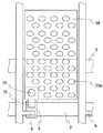
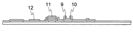
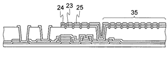
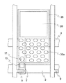
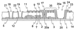
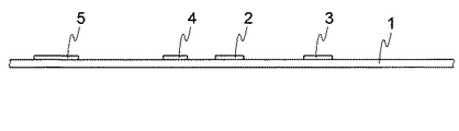
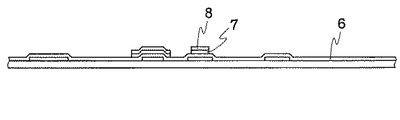
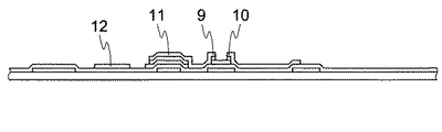
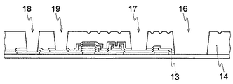
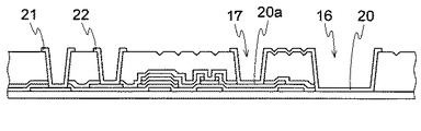
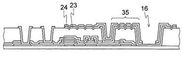
本発明の実施の形態1に係る反射型液晶表示装置の製法を図面を用いて説明する。図1は本発明の実施の形態1に係る反射型液晶表示装置の平面図、図2は断面図、そして図3〜9は工程図を示すものである。なお、図1おいて、反射画素電極35の領域内には、反射画素電極の凹形状部35aが多数設けられ、凹凸形状が形成されている。
前記の実施の形態1において、第1の金属薄膜としてAlNd−N/AlNd2層膜の代わりにNbを2.5〜20重量%添加したMoNb合金膜を用いたものである。好適な例として本実施の形態では、図3の工程において、第1の金属薄膜としてMoに5重量%のNbを添加したMoNb合金を公知のArガスを用いたスパッタリング法を用いて200nmの厚さで成膜し、公知のリン酸+硝酸+酢酸を含む溶液を用いてエッチングを行ない、ゲート電極2、補助容量電極3、ゲート配線4、およびゲート端子部5を形成した。前記公知のリン酸+硝酸+酢酸を含む溶液は、実施の形態1のAlNd−N/AlNd2層膜の場合と同じ溶液を用いることが可能である。その後、実施の形態1と同様に図4から図9の工程を経て本発明の実施の形態2に係わる反射型液晶表示装置を完成させた。
前述の実施の形態1において、第2の金属薄膜としてMoNb合金膜の代わりに、MoNb/AlNd/MoNb3層膜を用いたものである。最下層ならびに最上層にはMoにNbを2.5〜20重量%添加したMoNb合金膜を、中間層にはAlにNdを0.8〜5.0重量%添加したAlNd合金膜を用いると、従来公知のAlエッチャント(エッチング液)であるリン酸+硝酸+酢酸を含む薬液を用いてMoNb/AlNd/MoNb3層膜を1回のエッチングで一括エッチングすることが可能となるので好ましい。この場合は、層間で段差がなく滑らかな断面形状で3層膜をエッチングできる。好適な例として本実施の形態では、実施の形態1と同様に図3〜4の工程を経た後、図5の工程において、第2の金属薄膜としてMoに5重量%のNbを添加したMoNb合金、Alに2重量%のNdを添加したAlNd合金、そして再びMoに5重量%のNbを添加したMoNb合金を、公知のArガスを用いたスパッタリング法を用いて順次50nm、200nm、50nmの厚さで連続成膜してMoNb/AlNd/MoNb3層膜を形成した。そののち、公知のリン酸+硝酸+酢酸を含む溶液を用いてエッチングを行ない、ソース電極9、ドレイン電極10、ソース配線11およびソース端子12を形成した。このとき、3層膜のエッチング断面は段差もなく滑らかな形状となっていた。なお中間層はAlNd合金に限らず、たとえばAlに0.1〜1重量%のCuを添加したAlCu合金を用いることも可能である。
前述の実施の形態3において、さらに第1の金属薄膜としてAlNd−N/AlNd2層膜の代わりにMoに2.5〜20重量%のNbを添加したMoNb合金の200nm厚さの単層膜を用いたものである。この場合は、表1に示すように、実施の形態3に比べるとゲート配線抵抗は増大するものの、端子パッドのITO膜とのコンタクト抵抗は実施の形態3よりも低減させることができるので、表示不良に対するプロセスマージンを向上させることが可能である。
前述の実施の形態3において、第1の金属薄膜としてAlNd−N/AlNd2層膜の代わりに、Alに0.8〜5重量%のNdを添加したAlNd合金の上層にMoに2.5〜20重量%のNbを添加したMoNbを積層したMoNb/AlNd2層膜を用いたものである。好適な実施の形態としてここでは、図3の工程において、公知のArガスを用いたスパッタリング法にてAlに2重量%のNdを添加したAlNd合金を200nm、続けてMoに5重量%のNbを添加したMoNb合金を50nmの厚さで連続成膜し、MoNb/AlNd2層膜を形成した。その後、公知のAlエッチャントであるリン酸+硝酸+酢酸を含む薬液を用いてMoNb/AlNd2層膜を一括エッチングしてゲート電極2、補助容量電極3、ゲート配線4、およびゲート端子部5を形成した。前記公知のリン酸+硝酸+酢酸を含む溶液は、実施の形態1のAlNd−N/AlNd2層膜の場合と同じ溶液を用いることが可能である。その後、実施の形態1と同様に図4〜9の工程を経て本発明の実施の形態5に係わる反射型液晶表示装置を完成させた。
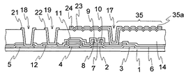
本発明の実施に形態6に係る半透過型液晶表示装置の製法を図を用いて説明する。図12は本発明の実施の形態6に係る半透過型液晶表示装置の平面図、図13は断面図、そして図14〜20は工程図を示すものである。
2 ゲート電極
3 補助容量電極
4 ゲート配線
5 ゲート端子
6 第1の絶縁膜
7 半導体膜
8 オーミックコンタクト膜
9 ソース電極
10 ドレイン電極
11 ソース配線
12 ソース端子
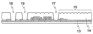
13 第2の絶縁膜
14 層間絶縁膜
15 画素反射部の凹凸形状部
16 画素透過部
17 第1のコンタクトホール
18 第2のコンタクトホール
19 第3のコンタクトホール
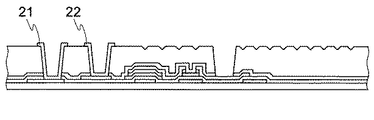
20 第1の画素電極(透過部)
21 ゲート端子パッド
22 ソース端子パッド
23 第2の画素電極(反射電極)の最下層膜
24 第2の画素電極(反射電極)の反射膜
25 第2の画素電極(反射電極)のITO電池反応防止用の最上層膜
26 Al
27 Cr
28 ITO
29 MoNb
35 反射画素電極
35a 反射画素電極の凹形状部
Claims (10)
- 透明性絶縁基板上に、第1の金属薄膜を成膜し、第1のフォトリソグラフィを用いて、
ゲート配線およびゲート電極を形成する第1の工程と、
ゲート絶縁膜、半導体能動膜およびオーミックコンタクト膜を順次成膜し、第2のフォトリソグラフィを用いて、半導体層を形成する第2の工程と、
第2の金属薄膜を成膜し、第3のフォトリソグラフィを用いて、ソース配線、ソース電極、ドレイン電極、および薄膜トランジスタのチャネル部を形成する第3の工程と、
層間絶縁膜を形成し、第4のフォトリソグラフィを用いて、画素電極部の表面に凹凸形状と、ゲート配線端子部、ソース配線端子部、およびドレイン電極に達するコンタクトホールをそれぞれ形成する第4の工程と、
第3の金属薄膜を成膜し、第5のフォトリソグラフィを用いて、画素電極を形成する第5の工程とを少なくとも含み、
前記第1の金属薄膜を、AlNd膜と、該AlNd膜の上層に形成された、チッ素(N)または、炭素(C)、または酸素(O)の少なくともひとつの元素を添加したAlNd膜とからなる二層膜とすることを特徴とする反射型液晶表示装置の製法。 - 前記第1の金属薄膜をMoにNbを添加した合金とする請求項1記載の反射型液晶表示装置の製法。
- 前記第2の金属薄膜をMoNb、またはMoNb/AlNd/MoNbの三層膜とする請求項1または2記載の反射型液晶表示装置の製法。
- 前記第3の金属薄膜を、Cr/AlNd/Crの三層膜を成膜し、パターニング後、上層Crを除去して、形成する請求項1、2または3記載の反射型液晶表示装置の製法。
- 前記第3の金属薄膜をAlCu/MoNbまたは、AlNd/MoNbの二層膜とする請求項1、2または3記載の反射型液晶表示装置の製法。
- 透明性絶縁基板上に、第1の金属薄膜を成膜し、第1のフォトリソグラフィを用いて、ゲート配線、ゲート電極を形成する第1の工程と、
ゲート絶縁膜、半導体能動膜およびオーミックコンタクト膜を順次成膜し、第2のフォトリソグラフィを用いて、半導体層を形成する第2の工程と、
第2の金属薄膜を成膜し、第3のフォトリソグラフィを用いて、ソース配線、ソース電極、ドレイン電極、および薄膜トランジスタのチャネル部を形成する第3の工程と、
層間絶縁膜を形成し、第4のフォトリソグラフィを用いて、画素反射電極部の表面に凹凸形状と、画素透過電極部の開口部と、ゲート配線端子部、ソース配線端子部、およびドレイン電極に達する、コンタクトホールを形成する第4の工程と、
透明導電膜を成膜し、第5のフォトリソグラフィを用いて、透過部画素電極、ならびに端子部パッドを形成する第5の工程と、
第3の金属薄膜を成膜し、第6のフォトリソグラフィを用いて、反射部画素電極を形成する第6の工程
とを少なくとも含み、
前記第1の金属薄膜を、AlNd膜と、該AlNd膜の上層に形成された、チッ素(N)または、炭素(C)または、酸素(O)の少なくともひとつの元素を添加したAlNd膜とからなる二層膜とすることを特徴とする半透過型液晶表示装置の製法。 - 前記第1の金属薄膜を、MoにNbを添加した合金とする請求項6記載の半透過型液晶表示装置の製法。
- 前記第2の金属薄膜を、MoNbまたは、MoNb/AlNd/MoNbの三層膜とする請求項6または7記載の半透過型液晶表示装置の製法。
- 前記第3の金属薄膜を、Cr/AlNd/Crの三層膜を成膜し、パターニング後、上層Crを除去して、形成する請求項6、7または8記載の半透過型液晶表示装置の製法。
- 前記第3の金属薄膜を、AlCu/MoNbまたは、AlNd/MoNbの二層膜とする請求項6、7または8記載の半透過型液晶表示装置の製法。
Priority Applications (4)
| Application Number | Priority Date | Filing Date | Title |
|---|---|---|---|
| JP2003356729A JP2005121908A (ja) | 2003-10-16 | 2003-10-16 | 反射型液晶表示装置および半透過型液晶表示装置ならびにこれらの製法 |
| TW093129563A TWI285757B (en) | 2003-10-16 | 2004-09-30 | Reflective and semi-transmission type liquid crystal display device and producing method thereof |
| KR1020040081757A KR100596044B1 (ko) | 2003-10-16 | 2004-10-13 | 반사형 액정표시장치 및 반투과형 액정표시장치와, 이들의제조방법 |
| CNB2004100841709A CN100421014C (zh) | 2003-10-16 | 2004-10-15 | 反射型和半透过型液晶显示装置的制造方法 |
Applications Claiming Priority (1)
| Application Number | Priority Date | Filing Date | Title |
|---|---|---|---|
| JP2003356729A JP2005121908A (ja) | 2003-10-16 | 2003-10-16 | 反射型液晶表示装置および半透過型液晶表示装置ならびにこれらの製法 |
Related Child Applications (1)
| Application Number | Title | Priority Date | Filing Date |
|---|---|---|---|
| JP2008057371A Division JP4782803B2 (ja) | 2008-03-07 | 2008-03-07 | 反射型液晶表示装置および半透過型液晶表示装置 |
Publications (1)
| Publication Number | Publication Date |
|---|---|
| JP2005121908A true JP2005121908A (ja) | 2005-05-12 |
Family
ID=34613880
Family Applications (1)
| Application Number | Title | Priority Date | Filing Date |
|---|---|---|---|
| JP2003356729A Pending JP2005121908A (ja) | 2003-10-16 | 2003-10-16 | 反射型液晶表示装置および半透過型液晶表示装置ならびにこれらの製法 |
Country Status (4)
| Country | Link |
|---|---|
| JP (1) | JP2005121908A (ja) |
| KR (1) | KR100596044B1 (ja) |
| CN (1) | CN100421014C (ja) |
| TW (1) | TWI285757B (ja) |
Cited By (4)
| Publication number | Priority date | Publication date | Assignee | Title |
|---|---|---|---|---|
| US7554634B2 (en) | 2005-11-04 | 2009-06-30 | Mitsubishi Electric Corporation | Thin film transistor array substrate, manufacturing method for the same, and transflective liquid crystal display |
| US7554119B2 (en) | 2005-01-31 | 2009-06-30 | Mitsubishi Denki Kabushiki Kaisha | Active matrix substrate and its manufacturing method |
| US7852443B2 (en) | 2007-05-11 | 2010-12-14 | Mitsubishi Electric Corporation | Display device and method having pixel and terminal parts where an organic resin film disposed thereon has a film thickness adjusting area so that the terminal part film thickness is thinner than the pixel part film thickness |
| US7910053B2 (en) | 2006-05-26 | 2011-03-22 | Mitsubishi Electric Corporation | Semiconductor device and active matrix display device |
Families Citing this family (7)
| Publication number | Priority date | Publication date | Assignee | Title |
|---|---|---|---|---|
| CN100525563C (zh) * | 2005-08-12 | 2009-08-05 | 中华映管股份有限公司 | 有机电致发光元件及其制造方法 |
| CN100371817C (zh) * | 2005-11-29 | 2008-02-27 | 友达光电股份有限公司 | 半穿透半反射式像素结构及其制造方法 |
| TWI858965B (zh) | 2006-05-16 | 2024-10-11 | 日商半導體能源研究所股份有限公司 | 液晶顯示裝置 |
| EP2124094A4 (en) * | 2007-01-31 | 2011-09-07 | Sharp Kk | LIQUID CRYSTAL DISPLAY DEVICE |
| KR102281850B1 (ko) | 2015-02-25 | 2021-07-26 | 삼성디스플레이 주식회사 | 터치 센서, 그 제조 방법 및 이를 포함하는 표시 장치 |
| CN104752444A (zh) * | 2015-04-24 | 2015-07-01 | 合肥鑫晟光电科技有限公司 | 显示基板及其制备方法、显示面板和显示装置 |
| EP3650936A4 (en) * | 2017-07-05 | 2020-09-09 | Toppan Printing Co., Ltd. | REFLECTIVE PHOTOMASK AND REFLECTIVE PHOTOMASK |
Family Cites Families (4)
| Publication number | Priority date | Publication date | Assignee | Title |
|---|---|---|---|---|
| US6369410B1 (en) * | 1997-12-15 | 2002-04-09 | Semiconductor Energy Laboratory Co., Ltd. | Semiconductor device and method of manufacturing the semiconductor device |
| JP4993830B2 (ja) * | 2000-11-11 | 2012-08-08 | 三星電子株式会社 | 反射型液晶表示装置及びその製造方法 |
| JP3859119B2 (ja) * | 2000-12-22 | 2006-12-20 | 日立金属株式会社 | 電子部品用薄膜配線 |
| CN1185685C (zh) * | 2001-09-20 | 2005-01-19 | 元太科技工业股份有限公司 | 薄膜晶体管液晶显示器及其制造方法 |
-
2003
- 2003-10-16 JP JP2003356729A patent/JP2005121908A/ja active Pending
-
2004
- 2004-09-30 TW TW093129563A patent/TWI285757B/zh not_active IP Right Cessation
- 2004-10-13 KR KR1020040081757A patent/KR100596044B1/ko not_active Expired - Fee Related
- 2004-10-15 CN CNB2004100841709A patent/CN100421014C/zh not_active Expired - Fee Related
Cited By (5)
| Publication number | Priority date | Publication date | Assignee | Title |
|---|---|---|---|---|
| US7554119B2 (en) | 2005-01-31 | 2009-06-30 | Mitsubishi Denki Kabushiki Kaisha | Active matrix substrate and its manufacturing method |
| US7923729B2 (en) | 2005-01-31 | 2011-04-12 | Mitsubishi Denki Kabushiki Kaisha | Active matrix substrate and its manufacturing method |
| US7554634B2 (en) | 2005-11-04 | 2009-06-30 | Mitsubishi Electric Corporation | Thin film transistor array substrate, manufacturing method for the same, and transflective liquid crystal display |
| US7910053B2 (en) | 2006-05-26 | 2011-03-22 | Mitsubishi Electric Corporation | Semiconductor device and active matrix display device |
| US7852443B2 (en) | 2007-05-11 | 2010-12-14 | Mitsubishi Electric Corporation | Display device and method having pixel and terminal parts where an organic resin film disposed thereon has a film thickness adjusting area so that the terminal part film thickness is thinner than the pixel part film thickness |
Also Published As
| Publication number | Publication date |
|---|---|
| TWI285757B (en) | 2007-08-21 |
| KR20050036758A (ko) | 2005-04-20 |
| KR100596044B1 (ko) | 2006-07-05 |
| CN100421014C (zh) | 2008-09-24 |
| CN1609689A (zh) | 2005-04-27 |
| TW200525209A (en) | 2005-08-01 |
Similar Documents
| Publication | Publication Date | Title |
|---|---|---|
| US7470571B2 (en) | Thin film transistor array substrate and method of producing the same | |
| JP3785900B2 (ja) | 液晶表示装置とその製造方法 | |
| KR100698988B1 (ko) | 액정 표시 장치와 그 제조 방법 | |
| JP3431856B2 (ja) | 液晶表示装置の製造方法 | |
| KR100698950B1 (ko) | 박막 트랜지스터 어레이 기판의 제조방법 | |
| JP5215620B2 (ja) | 半導体デバイス、表示装置及び半導体デバイスの製造方法 | |
| JP3670577B2 (ja) | 液晶表示装置およびその製造方法 | |
| US7733446B2 (en) | Semitransmissive liquid crystal display device and manufacturing method thereof | |
| CN100555641C (zh) | Tft阵列衬底及其制造方法、以及使用该衬底的显示装置 | |
| JP2005121908A (ja) | 反射型液晶表示装置および半透過型液晶表示装置ならびにこれらの製法 | |
| JP3513409B2 (ja) | 液晶表示装置およびその製造方法 | |
| KR100802457B1 (ko) | 액정표시장치 및 그 제조 방법 | |
| JP4782803B2 (ja) | 反射型液晶表示装置および半透過型液晶表示装置 | |
| US20070096098A1 (en) | Conductive structure, manufacturing method for conductive structure, element substrate, and manufacturing method for element substrate | |
| KR100832511B1 (ko) | 박막 트랜지스터 어레이 기판 및 그 제조방법과, 반투과형액정 표시장치 | |
| JP2012129444A (ja) | アクティブマトリックス基板、及び液晶装置 | |
| JP2006330021A (ja) | 液晶表示装置 | |
| JPH1144887A (ja) | 表示装置用反射電極基板 | |
| JP4219717B2 (ja) | 表示装置の製造方法、液晶表示装置並びに金属膜のパターニング方法。 | |
| JP4338481B2 (ja) | 液晶表示装置用薄膜トランジスタの製法および液晶表示装置用薄膜トランジスタ | |
| CN100426062C (zh) | 半透射型tft阵列衬底以及半透射型液晶显示装置 | |
| JPH10307303A (ja) | 液晶表示基板、その製造方法および液晶表示装置 | |
| JP2005266475A (ja) | 半透過型液晶表示装置 |
Legal Events
| Date | Code | Title | Description |
|---|---|---|---|
| A621 | Written request for application examination |
Free format text: JAPANESE INTERMEDIATE CODE: A621 Effective date: 20050617 |
|
| A977 | Report on retrieval |
Free format text: JAPANESE INTERMEDIATE CODE: A971007 Effective date: 20070727 |
|
| A131 | Notification of reasons for refusal |
Free format text: JAPANESE INTERMEDIATE CODE: A131 Effective date: 20070814 |
|
| A521 | Written amendment |
Free format text: JAPANESE INTERMEDIATE CODE: A523 Effective date: 20070921 |
|
| A711 | Notification of change in applicant |
Free format text: JAPANESE INTERMEDIATE CODE: A711 Effective date: 20071106 |
|
| A02 | Decision of refusal |
Free format text: JAPANESE INTERMEDIATE CODE: A02 Effective date: 20080108 |