JP2004363604A - Nonvolatile memory device including one switching element and one resistor and method for manufacturing the same - Google Patents
Nonvolatile memory device including one switching element and one resistor and method for manufacturing the same Download PDFInfo
- Publication number
- JP2004363604A JP2004363604A JP2004164659A JP2004164659A JP2004363604A JP 2004363604 A JP2004363604 A JP 2004363604A JP 2004164659 A JP2004164659 A JP 2004164659A JP 2004164659 A JP2004164659 A JP 2004164659A JP 2004363604 A JP2004363604 A JP 2004363604A
- Authority
- JP
- Japan
- Prior art keywords
- data storage
- material layer
- storage material
- memory device
- nonvolatile memory
- Prior art date
- Legal status (The legal status is an assumption and is not a legal conclusion. Google has not performed a legal analysis and makes no representation as to the accuracy of the status listed.)
- Granted
Links
Images


Classifications
-
- G—PHYSICS
- G11—INFORMATION STORAGE
- G11C—STATIC STORES
- G11C11/00—Digital stores characterised by the use of particular electric or magnetic storage elements; Storage elements therefor
- G11C11/02—Digital stores characterised by the use of particular electric or magnetic storage elements; Storage elements therefor using magnetic elements
- G11C11/14—Digital stores characterised by the use of particular electric or magnetic storage elements; Storage elements therefor using magnetic elements using thin-film elements
- G11C11/15—Digital stores characterised by the use of particular electric or magnetic storage elements; Storage elements therefor using magnetic elements using thin-film elements using multiple magnetic layers
-
- G—PHYSICS
- G11—INFORMATION STORAGE
- G11C—STATIC STORES
- G11C13/00—Digital stores characterised by the use of storage elements not covered by groups G11C11/00, G11C23/00, or G11C25/00
- G11C13/0002—Digital stores characterised by the use of storage elements not covered by groups G11C11/00, G11C23/00, or G11C25/00 using resistive RAM [RRAM] elements
- G11C13/0007—Digital stores characterised by the use of storage elements not covered by groups G11C11/00, G11C23/00, or G11C25/00 using resistive RAM [RRAM] elements comprising metal oxide memory material, e.g. perovskites
-
- H—ELECTRICITY
- H10—SEMICONDUCTOR DEVICES; ELECTRIC SOLID-STATE DEVICES NOT OTHERWISE PROVIDED FOR
- H10B—ELECTRONIC MEMORY DEVICES
- H10B63/00—Resistance change memory devices, e.g. resistive RAM [ReRAM] devices
- H10B63/20—Resistance change memory devices, e.g. resistive RAM [ReRAM] devices comprising selection components having two electrodes, e.g. diodes
-
- H—ELECTRICITY
- H10—SEMICONDUCTOR DEVICES; ELECTRIC SOLID-STATE DEVICES NOT OTHERWISE PROVIDED FOR
- H10B—ELECTRONIC MEMORY DEVICES
- H10B63/00—Resistance change memory devices, e.g. resistive RAM [ReRAM] devices
- H10B63/30—Resistance change memory devices, e.g. resistive RAM [ReRAM] devices comprising selection components having three or more electrodes, e.g. transistors
-
- H—ELECTRICITY
- H10—SEMICONDUCTOR DEVICES; ELECTRIC SOLID-STATE DEVICES NOT OTHERWISE PROVIDED FOR
- H10N—ELECTRIC SOLID-STATE DEVICES NOT OTHERWISE PROVIDED FOR
- H10N70/00—Solid-state devices without a potential-jump barrier or surface barrier, and specially adapted for rectifying, amplifying, oscillating or switching
- H10N70/20—Multistable switching devices, e.g. memristors
-
- H—ELECTRICITY
- H10—SEMICONDUCTOR DEVICES; ELECTRIC SOLID-STATE DEVICES NOT OTHERWISE PROVIDED FOR
- H10N—ELECTRIC SOLID-STATE DEVICES NOT OTHERWISE PROVIDED FOR
- H10N70/00—Solid-state devices without a potential-jump barrier or surface barrier, and specially adapted for rectifying, amplifying, oscillating or switching
- H10N70/801—Constructional details of multistable switching devices
- H10N70/821—Device geometry
- H10N70/826—Device geometry adapted for essentially vertical current flow, e.g. sandwich or pillar type devices
-
- H—ELECTRICITY
- H10—SEMICONDUCTOR DEVICES; ELECTRIC SOLID-STATE DEVICES NOT OTHERWISE PROVIDED FOR
- H10N—ELECTRIC SOLID-STATE DEVICES NOT OTHERWISE PROVIDED FOR
- H10N70/00—Solid-state devices without a potential-jump barrier or surface barrier, and specially adapted for rectifying, amplifying, oscillating or switching
- H10N70/801—Constructional details of multistable switching devices
- H10N70/881—Switching materials
- H10N70/883—Oxides or nitrides
- H10N70/8833—Binary metal oxides, e.g. TaOx
-
- G—PHYSICS
- G11—INFORMATION STORAGE
- G11C—STATIC STORES
- G11C2213/00—Indexing scheme relating to G11C13/00 for features not covered by this group
- G11C2213/30—Resistive cell, memory material aspects
- G11C2213/32—Material having simple binary metal oxide structure
-
- G—PHYSICS
- G11—INFORMATION STORAGE
- G11C—STATIC STORES
- G11C2213/00—Indexing scheme relating to G11C13/00 for features not covered by this group
- G11C2213/70—Resistive array aspects
- G11C2213/79—Array wherein the access device being a transistor
Abstract
Description
本発明は、不揮発性メモリ装置に係り、より詳細には一つのトランジスタとデータが記録される一つの抵抗体を含む不揮発性メモリ装置およびその製造方法に関する。 The present invention relates to a nonvolatile memory device, and more particularly, to a nonvolatile memory device including one transistor and one resistor in which data is recorded, and a method of manufacturing the same.
PRAMは、一つのトランジスタと一つの抵抗体(以下、1T−1Rという)とで構成される従来の代表的不揮発性メモリ装置中の一つである。 A PRAM is one of the conventional typical nonvolatile memory devices including one transistor and one resistor (hereinafter, referred to as 1T-1R).
PRAMに使われる抵抗体は、カルコゲナイド(calcogenide)抵抗体である。この抵抗体の物質状態は形成温度によって非晶質(Amorphous)または結晶質(Crystalline)になる。カルコゲナイド抵抗体の抵抗は物質状態が非晶質である場合には高く、結晶質である場合には低い。 The resistor used in the PRAM is a chalcogenide resistor. The material state of the resistor becomes amorphous (Amorphous) or crystalline (Crystalline) depending on the forming temperature. The resistance of the chalcogenide resistor is high when the material state is amorphous, and low when the material state is crystalline.
このように、PRAMはカルコゲナイド抵抗体の物質状態が変わる時、その抵抗が変わるという現象を利用してデータを書き込み、読取る不揮発性メモリ装置である。 As described above, the PRAM is a non-volatile memory device that writes and reads data by using the phenomenon that the resistance changes when the material state of the chalcogenide resistor changes.
PRAMのような従来の不揮発性メモリ装置の場合、優れた耐エッチング性を有する抵抗体を用いる既存のDRAM工程によっては、エッチングし難い。たとえエッチングが可能であっても長時間がかかる。このため、従来の1T−1Rを含む不揮発性メモリ装置の場合、生産性が低くなって製品コストが上昇し、市場での製品競争力を失うおそれがある。 In the case of a conventional non-volatile memory device such as a PRAM, it is difficult to etch by a conventional DRAM process using a resistor having excellent etching resistance. Even if etching is possible, it takes a long time. For this reason, in the case of the conventional nonvolatile memory device including the 1T-1R, the productivity is lowered, the product cost is increased, and the product competitiveness in the market may be lost.
本発明は、前記従来技術の問題点を解決するためになされたものであって、本発明の目的は、既存のDRAM工程をそのまま使用できるために大量生産および製品コストを低くすることができ、集積度に抵抗体のメモリ特性が影響を受けない一つのスイッチング素子(Trまたはダイオード)と一つの抵抗体とを含む不揮発性メモリ装置を提供することである。 The present invention has been made to solve the above-mentioned problems of the related art, and an object of the present invention is to enable mass production and product cost to be reduced because existing DRAM processes can be used as they are, An object of the present invention is to provide a nonvolatile memory device including one switching element (Tr or diode) and one resistor in which the memory characteristics of the resistor are not affected by the degree of integration.
本発明の他の目的は、前記不揮発性メモリ装置の製造方法を提供することである。 It is another object of the present invention to provide a method for manufacturing the nonvolatile memory device.
前記技術的課題を達成するために、本発明は、トランジスタとトランジスタのドレーンに連結されているデータ貯蔵部とを備える不揮発性メモリ装置を提供する。 According to an aspect of the present invention, there is provided a nonvolatile memory device including a transistor and a data storage unit connected to a drain of the transistor.
前記データ貯蔵部は、データ貯蔵物質層を含むことができる。前記データ貯蔵物質層は、所定の第1電圧範囲で第1抵抗特性を持ち、所定の第2電圧範囲で第2抵抗特性を持ち得る。前記第1電圧範囲は前記第2電圧範囲と異なり、前記第1抵抗特性は前記第2抵抗特性と異なる。 The data storage unit may include a data storage material layer. The data storage material layer may have a first resistance characteristic in a first predetermined voltage range and a second resistance characteristic in a second predetermined voltage range. The first voltage range is different from the second voltage range, and the first resistance characteristic is different from the second resistance characteristic.
前記データ貯蔵物質層の上部および下部にそれぞれ上部および下部電極が備わっている。 Upper and lower electrodes are provided on the upper and lower portions of the data storage material layer, respectively.
本発明の他の実施の形態によれば、前記下部電極と前記基板との間に層間絶縁層が形成されており、前記層間絶縁層に前記ドレーンが露出されるコンタクトホールが形成されており、前記コンタクトホールは導電性プラグで充填されている。 According to another embodiment of the present invention, an interlayer insulating layer is formed between the lower electrode and the substrate, and a contact hole exposing the drain is formed in the interlayer insulating layer, The contact hole is filled with a conductive plug.
前記データ貯蔵物質層は、前記所定の電圧範囲で抵抗が急激に高くなる遷移金属酸化膜である。 The data storage material layer is a transition metal oxide film whose resistance rapidly increases in the predetermined voltage range.
また、本発明は前記技術的課題を達成するために、スイッチング機能を有する一つのダイオード(以下、1Dという)とこれに連結されている一つのデータ貯蔵部と、を備える不揮発性メモリ装置を提供する。 According to another aspect of the present invention, there is provided a nonvolatile memory device including one diode having a switching function (hereinafter referred to as 1D) and one data storage unit connected to the diode. I do.
ここで、前記データ貯蔵部は、前記データ貯蔵物質層を含むものであって、詳細な構成は前述の通りである。 Here, the data storage unit includes the data storage material layer, and the detailed configuration is as described above.
また、本発明は前記技術的課題を達成するために、基板と、前記基板に形成されたトランジスタ、および前記トランジスタのドレーンに連結されているデータ貯蔵部とを備える1T−1Rからなる不揮発性メモリ装置の製造方法において、前記データ貯蔵部は、下部電極、データ貯蔵物質層、および上部電極を順次に積層して形成しており、前記データ貯蔵物質層は、所定の電圧範囲で現れる抵抗特性が別の電圧範囲で現れる抵抗特性と全く異なる物質膜で形成することを特徴とする不揮発性メモリ装置の製造方法を提供する。 According to another embodiment of the present invention, there is provided a nonvolatile memory comprising a 1T-1R including a substrate, a transistor formed on the substrate, and a data storage unit connected to a drain of the transistor. In the device manufacturing method, the data storage unit is formed by sequentially stacking a lower electrode, a data storage material layer, and an upper electrode, and the data storage material layer has a resistance characteristic that appears in a predetermined voltage range. Provided is a method for manufacturing a nonvolatile memory device, which is formed using a material film completely different from a resistance characteristic appearing in another voltage range.
前記物質膜は、前記所定の電圧範囲で抵抗が急激に高くなる遷移金属酸化膜で形成する。 The material film is formed of a transition metal oxide film whose resistance rapidly increases in the predetermined voltage range.
また、本発明は前記技術的課題を達成するために、半導体基板にスイッチングダイオードを形成する段階と、前記半導体基板に前記スイッチングダイオードと連結されるようにデータ貯蔵部とを形成する段階とを含み、前記データ貯蔵部は前記スイッチングダイオードと連結される下部電極、データ貯蔵物質層、および上部電極を順次に積層して形成することを特徴とする不揮発性メモリ装置の製造方法を提供する。 In order to achieve the above technical object, the present invention includes forming a switching diode on a semiconductor substrate, and forming a data storage unit on the semiconductor substrate so as to be connected to the switching diode. The data storage unit may be formed by sequentially stacking a lower electrode connected to the switching diode, a data storage material layer, and an upper electrode.
この時、前記データ貯蔵物質層は、所定の電圧範囲で現れる抵抗特性が他の電圧範囲で現れる抵抗特性と全く異なる物質膜で形成することが望ましい。前記物質膜は前述の通りである。 In this case, the data storage material layer is preferably formed of a material film having a resistance characteristic that appears in a predetermined voltage range and is completely different from a resistance characteristic that appears in another voltage range. The material film is as described above.
本発明によれば、遷移金属酸化膜を抵抗体として利用するために、既存のDRAM工程をそのまま使用できる。したがって製品の生産性が高まって製品コストを節減することができる。また、抵抗体の抵抗変化を用いてデータを書き込み、読取るので、集積度が高くなって抵抗体のサイズが小さくなっても抵抗体のメモリ特性は影響を受けない。また、抵抗体に記録されたデータは非破壊的に読取られるために、データが読取られた後にも前記抵抗体は前記データが読取られる前の状態になり、動作電圧も低くなる。これは、データを読取った後に一般的に行われる再貯蔵(restoration)過程が必要ないことを意味する。 According to the present invention, the existing DRAM process can be used as it is because the transition metal oxide film is used as the resistor. Therefore, the productivity of the product is increased and the product cost can be reduced. Further, since data is written and read using the resistance change of the resistor, the memory characteristics of the resistor are not affected even if the degree of integration is increased and the size of the resistor is reduced. Further, since the data recorded on the resistor is nondestructively read, the resistor is in a state before the data is read even after the data is read, and the operating voltage is reduced. This means that a restoring process that is generally performed after reading data is not required.
以下、本発明の実施の形態による一つのトランジスタと一つの抵抗体とで構成された不揮発性メモリ装置およびその製造方法を添付した図面に基づいて詳細に説明する。図面において層および領域等の厚さは明細書の明確性のために誇張して示したものである。 Hereinafter, a nonvolatile memory device including one transistor and one resistor according to an embodiment of the present invention and a method of manufacturing the same will be described in detail with reference to the accompanying drawings. In the drawings, the thickness of layers and regions are exaggerated for clarity of the specification.
図1を参照すれば、本発明の実施の形態による一つのトランジスタと一つの抵抗体で構成された不揮発性メモリ装置は基板40、基板40に形成されたトランジスタ、および前記トランジスタの一領域に連結されるように備わったデータ貯蔵部Sを含む。前記トランジスタは、基板40の表層に形成されており、導電性不純物がドーピングされたソース42およびドレーン44と、ソース42およびドレーン44間の基板40上、即ちチャンネル領域46上に形成されたゲート積層物48、50とよりなる。ゲート積層物48、50は、順次に積層されたゲート絶縁膜48とゲート電極50とで構成される。
Referring to FIG. 1, a nonvolatile memory device including one transistor and one resistor according to an embodiment of the present invention is connected to a
データ貯蔵部Sはドレーン44上に形成されている。データ貯蔵部Sは、ドレーン44と直接接触する下部電極52、下部電極52上に積層されているデータ貯蔵物質層54、およびデータ貯蔵物質層54上に積層されている上部電極56で構成される。データ貯蔵物質層54は、電圧や電流パルスの大きさと方向によって抵抗が変化する物質層、すなわち可変抵抗物質層である。データ貯蔵物質層54として使用できる可変抵抗物質層には、ニッケル酸化膜(NiO)、バナジウム酸化膜(V2O5)、亜鉛酸化膜(ZnO)、ニオブ酸化膜(Nb2O5)、チタン酸化膜(TiO2)、タングステン酸化膜(WO3)またはコバルト酸化膜(CoO)等のような遷移金属酸化膜が望ましい。
The data storage unit S is formed on the
後述するが、このような遷移金属酸化膜は次の特性を持っている。 As will be described later, such a transition metal oxide film has the following characteristics.
すなわち、前記遷移金属酸化膜に特定値の電圧や電流が印加されて前記遷移金属酸化膜の抵抗が特定値になった場合、前記遷移金属酸化膜に外部から新たな特定値の電圧および電流が印加されるまで前記遷移金属酸化膜の特定抵抗値はそのまま維持される。 That is, when a specific voltage or current is applied to the transition metal oxide film and the resistance of the transition metal oxide film reaches a specific value, a new specific value of voltage and current is externally applied to the transition metal oxide film. Until the voltage is applied, the specific resistance value of the transition metal oxide film is maintained as it is.
続いて、基板40上に前記トランジスタを覆い、データ貯蔵部Sを取り囲む層間絶縁層60が形成されている。そして、層間絶縁層60の上部電極56上に形成された部分は除去されて上部電極56の上部面は露出される。層間絶縁層60上にプレート電極58が積層されている。プレート電極58は、上部電極56の露出された部分の全面と連結されている。プレート電極58と上部電極56とは同一物質でありうる。電流増幅器61は、ドレーン44に連結されてドレーン電流Idをセンシングして増幅する。
Subsequently, an
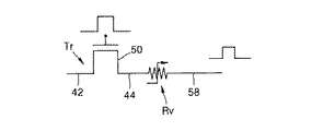
図2は、図1に示した不揮発性メモリ装置の回路図である。図2において参照符号Trは前記のトランジスタを示し、Rvはデータ貯蔵物質層54に該当する可変抵抗体を示す。
FIG. 2 is a circuit diagram of the nonvolatile memory device shown in FIG. In FIG. 2, reference numeral Tr indicates the transistor, and Rv indicates a variable resistor corresponding to the data
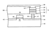
図3は、図1に示したメモリ装置の変形例を示す。 FIG. 3 shows a modification of the memory device shown in FIG.
具体的に、図3を参照すれば、基板40上にソース42、ゲート積層物48、50、およびドレーン44を覆う第1層間絶縁層62が積層されている。第1層間絶縁層62は平面である。第1層間絶縁層62にドレーン44が露出されるコンタクトホールh1が形成されている。コンタクトホールh1は、導電性プラグ64で充填されている。第1層間絶縁層62上に導電性プラグ64の全面と接触されるデータ貯蔵部Sが積層されている。第1層間絶縁層62上にデータ貯蔵部Sを覆う第2層間絶縁層66が積層されている。第2層間絶縁層66にデータ貯蔵部Sの上部電極56が露出されるビアホールh2が形成されている。第2層間絶縁層66上にビアホールh2を充填するプレート電極58が形成されている。
Specifically, referring to FIG. 3, a first
一方、図示していないが、データ貯蔵部Sの構成要素はスタックタイプでなくてもよい。 On the other hand, although not shown, the components of the data storage unit S may not be of the stack type.
例えば、データ貯蔵部Sの下部電極52がシリンダ状であり、データ貯蔵物質層54が下部電極52の表面に形成され得る。または下部電極52がシリンダ状であり、このような下部電極52の表面にデータ貯蔵物質層54が形成されてもよい。
For example, the
次いで、図4および図5に基づいて前記の不揮発性メモリ装置のデータ貯蔵部Sの特性について説明する。 Next, the characteristics of the data storage unit S of the nonvolatile memory device will be described with reference to FIGS.
図4は、データ貯蔵部Sのデータ貯蔵物質層54がニッケル酸化膜である場合であり、図5はデータ貯蔵物質層54がチタン酸化膜の場合である。
FIG. 4 illustrates a case where the data
図4および図5において、横軸はデータ貯蔵部Sに印加される電圧を示し、縦軸は前記電圧によるソース42とドレーン44間に流れるドレーン電流Idを示す。
4 and 5, the horizontal axis indicates the voltage applied to the data storage unit S, and the vertical axis indicates the drain current Id flowing between the
図4における参照符号G1は、データ貯蔵部Sの抵抗、さらに正確にはデータ貯蔵物質層54の抵抗値が低くなった時に適用される電流−電圧曲線を示す第1グラフである。そして、参照符号G2は、データ貯蔵物質層54の抵抗が高くなった場合、またはドレーン電流値が低い場合に適用される電流−電圧曲線を示す第2グラフである。
4 is a first graph showing a current-voltage curve applied when the resistance of the data storage unit S, more precisely, the resistance value of the data
第1グラフG1を参照すれば、データ貯蔵物質層54に印加される電圧に比例してドレーン電流Idが変化することが分かる。ところが、データ貯蔵物質層54に印加される電圧が第1電圧V1(V1>0)になると、データ貯蔵物質層54の抵抗が突然に大きくなり、データ貯蔵物質層54のドレーン電流Idは急激に小さくなることが分かる。データ貯蔵物質層54のこのような状態は、データ貯蔵物質層54に第2電圧V2(V2>V1)が印加されるまで維持される。すなわち、データ貯蔵物質層54への電圧の印加中、△V(V1〜V2)の間はデータ貯蔵物質層54の抵抗が急激に高くなる。続いて、データ貯蔵物質層54に印加される電圧が第2電圧V2より大きくなると、データ貯蔵物質層54の抵抗は急激に低くなる。データ貯蔵物質層54のドレーン電流Id変化は、データ貯蔵物質層54に第1電圧V1より小さい電圧が印加される時の変化と同じように、印加される電圧に比例する。
Referring to the first graph G1, it can be seen that the drain current Id changes in proportion to the voltage applied to the data
すなわち、それに印加される電圧値が第1電圧V1より大きいかまたは小さい場合、データ貯蔵物質層54の電流は、それに印加される電圧値に従って変化する。
That is, when the voltage applied to the data
具体的に、データ貯蔵物質層54に第3電圧(V3>V2)を印加して、データ貯蔵物質層54が第1抵抗値を持つようになった後、データ貯蔵物質層54に第1電圧V1より小さい電圧を印加した場合は、データ貯蔵物質層54から第1グラフG1に示したような電流値(抵抗値)が測定された(以下、第1ケースという)。
More specifically, a third voltage (V3> V2) is applied to the data
一方、データ貯蔵物質層54に所定の電圧(V1≦V≦V2)を印加して、図4に示したようにデータ貯蔵物質層54が第2抵抗値(>第1抵抗値)を持つようになった後、データ貯蔵物質層54に第1電圧V1より小さい電圧を印加した場合は、データ貯蔵物質層54から第2グラフG2に示したような電流値(抵抗値)が測定された(以下、第2ケースという)。
Meanwhile, a predetermined voltage (V1 ≦ V ≦ V2) is applied to the data
前記第2ケースの所定電圧で測定された電流値は、前記第1ケースで測定された電流値より非常に小さい。抵抗値の場合は反対になる。これは、第1電圧V1より小さい所定の電圧でデータ貯蔵物質層54から相異なる二電流値が測定できることを意味する。前記二電流値は各々データ貯蔵物質層54に記録されたデータ“0”および“1”に該当する。
The current value measured at the predetermined voltage in the second case is much smaller than the current value measured in the first case. The opposite is true for resistance values. This means that two different current values can be measured from the data
すなわち、前記第1ケースはデータ貯蔵物質層54に記録されるデータ“1”に対応し、前記第2ケースはデータ貯蔵物質層54に記録されるデータ“0”に対応する。
That is, the first case corresponds to data "1" recorded in the data
前記第1および第2ケースに対するデータ値の設定は任意的である。したがって、前記第1ケースはデータ“0”を書き込み、読取る場合であり、前記第2ケースはデータ“1”を書き込み、読取る場合であってもよい。 The setting of data values for the first and second cases is optional. Therefore, the first case may be a case where data "0" is written and read, and the second case may be a case where data "1" is written and read.
一方、データ貯蔵物質層54の電圧−電流特性は、データ貯蔵物質層54がチタン酸化膜である場合、図5に示したように図4に示した電圧−電流特性と異なることが分かる。
On the other hand, when the data
図5において、第3および第5グラフG4、G5は、データ貯蔵部Sに負の電圧、例えば第5電圧V5より小さい負の電圧V(|V|≧|V5|>0)が印加された後、データ貯蔵物質層54の抵抗値は急激に低くなるが、この時、適用される電流−電圧曲線を示す。また、第4および第6グラフG4、G6は、データ貯蔵部Sに正の電圧、例えば第4電圧V4より大きい電圧V(V≧V4>0)が印加された後、データ貯蔵物質層54の抵抗が急激に大きくなった場合(ドレーン電流値が低い時)、適用される電流−電圧曲線を示す。
In FIG. 5, in the third and fifth graphs G4 and G5, a negative voltage, for example, a negative voltage V (| V | ≧ | V5 |> 0) smaller than the fifth voltage V5 is applied to the data storage unit S. Thereafter, the resistance value of the data
第4および第6グラフG4、G6を参照すれば、第4電圧V4より大きい電圧がデータ貯蔵部Sに印加された後、データ貯蔵物質層54の電圧−電流特性は正の電圧領域では第4グラフG4に沿って、負の電圧領域では第6グラフG6に沿って変化する。したがって、データ貯蔵部Sに第4電圧V4より大きい電圧が印加された後に、データ貯蔵物質層54はデータ貯蔵部Sに負の第5電圧V5が印加されるまで高い抵抗特性を維持する(以下、第3ケースという)。
Referring to the fourth and sixth graphs G4 and G6, after a voltage higher than the fourth voltage V4 is applied to the data storage unit S, the voltage-current characteristic of the data
また、第3および第5グラフG3、G5を参照すれば、データ貯蔵部Sに第5電圧V5より小さい電圧が印加された後、データ貯蔵物質層54の電圧−電流特性は負の電圧領域では第5グラフG5に沿って、正の電圧領域では第3グラフG3に沿って変化する。したがって、データ貯蔵部Sに第5電圧V5より小さい電圧が印加された後にデータ貯蔵物質層54はデータ貯蔵部Sに第4電圧V4が印加されるまで低い抵抗特性を維持する(以下、第4ケースという)。
Referring to the third and fifth graphs G3 and G5, after a voltage lower than the fifth voltage V5 is applied to the data storage unit S, the voltage-current characteristic of the data
前記第3および第4ケースにおいて、データ貯蔵物質層54は、第5電圧V5と第4電圧V4間の有効な所定電圧で二つの電流値(または二つの抵抗値)を有することがわかる。これは、データ貯蔵物質層54が前記二つの電圧の間で二つの状態であることを意味し、二つの状態のうち一つはデータ“1”、残りはデータ“0”に対応できることを意味する。
In the third and fourth cases, it can be seen that the data
データ貯蔵物質層54のこのような状態は、データ貯蔵部Sに第4電圧V4以上、または第5電圧V5以下の電圧をデータ貯蔵部Sに印加することによって決定されるが、データ貯蔵物質層54の前記状態を測定するために印加される電圧は、第4電圧V4より小さいか第5電圧V5より大きいため、データ貯蔵物質層54の状態を測定した後(読取った後)にもデータ貯蔵物質層54の状態は測定前状態のままで維持される。
Such a state of the data
これは、データ貯蔵物質層54に保存されたデータを読取った後にもデータ貯蔵物質層54に保存されたデータは読取る前の状態で正常に維持されることを意味する。
This means that even after the data stored in the data
図6および図7は、データ貯蔵物質層54にデータを書き込み、書き込まれたデータを読取るために、または消去するためにデータ貯蔵部Sに印加される電圧パルスの例を示す。
6 and 7 show examples of voltage pulses applied to the data storage unit S in order to write data in the data
図6はデータ貯蔵物質層54がニッケル酸化膜である場合、データ貯蔵物質層54に印加される電圧パルスを、図7はデータ貯蔵物質層54がチタン酸化膜である場合、データ貯蔵物質層54に印加される電圧パルスをそれぞれ示す。
6 shows a voltage pulse applied to the data
まず、図6を参照すれば、第2書込み電圧パルスVw2がデータ貯蔵物質層54にデータ、例えば“1”を書込むためにデータ貯蔵物質層54に印加される。第2書込み電圧パルスVw2は図4の第3電圧V3に該当する値である。第3読取り電圧パルスVr3は、データ貯蔵物質層54に書込まれたデータ“1”を読取るためにデータ貯蔵物質層54に印加される。第3読取り電圧パルスVr3は図4の第1電圧V1より低い値に該当する。
First, referring to FIG. 6, a second write voltage pulse Vw2 is applied to the data
図4の第1グラフG1を参照すれば、データ貯蔵物質層54に第3電圧V3が印加される場合、データ貯蔵物質層54は抵抗が低い状態となる。このような状態はデータ貯蔵物質層54に第1電圧V1より小さい電圧が印加される時にもそのまま維持される。したがって、第1電圧V1より小さい電圧に該当する図6の第3読取り電圧パルスVr3をデータ貯蔵物質層54に印加した場合、データ貯蔵物質層54から測定される電流値はデータ貯蔵物質層54に第1電圧V1と第2電圧V2間の電圧を印加した場合に測定される電流値よりはるかに大きくなる。このような結果からデータ貯蔵物質層54にデータ“1”が記録されていることが分かる。
Referring to the first graph G1 of FIG. 4, when the third voltage V3 is applied to the data
続いて、図6において第3書込み電圧パルスVE2がデータ貯蔵物質層54にデータ“0”を記録するためにデータ貯蔵物質層54に印加される。第3書込み電圧パルスVE2は、図4の第1電圧V1と第2電圧V2間の電圧に該当する。データ貯蔵物質層54に第2書込み電圧パルスVw2より小さい第3書込み電圧パルスVE2が印加される場合、データ貯蔵物質層54の抵抗は急激に高くなる(図4参照)。データ貯蔵物質層54のこのような状態はデータ貯蔵物質層54に印加される電圧パルスが第1電圧V1より小さい場合もそのまま維持される(図4の第2グラフG2参照)。
Subsequently, in FIG. 6, a third write voltage pulse VE2 is applied to the data
図6において第4読取り電圧パルスVR4がデータ貯蔵物質層54からデータ“0”を読取るためにデータ貯蔵物質層54に印加される。第4読取り電圧パルスVR4は図4の第1電圧V1より小さい電圧に該当する。そして、データ“0”を読取るため、データ貯蔵物質層54に第4読取り電圧パルスVR4を印加した時、データ貯蔵物質層54から測定される電流値はデータ“1”を読取る場合よりはるかに小さくなる。
In FIG. 6, a fourth read voltage pulse VR4 is applied to the data
一方、データ貯蔵物質層54に書込まれたデータは、データ貯蔵部Sに前記データを書込む時に印加した電圧パルスと逆極性の電圧パルスを印加することによって簡単に消去できる。
On the other hand, the data written in the data
図7を参照すれば、第1書込み電圧パルスVw1がデータ貯蔵物質層54に所定のデータ、例えば“1”を書込むためにデータ貯蔵物質層54に印加される。
Referring to FIG. 7, a first write voltage pulse Vw1 is applied to the data
次いで、第1書込み電圧パルスVw1が印加されてデータ貯蔵物質層54に書込まれたデータ“1”を読取るために、第1読取り電圧パルスVR1がデータ貯蔵部Sに印加される。第1読取り電圧パルスVR1は、第1書込み電圧パルスVw1より小さく(VR1<Vw1)、0より大きくて第4電圧V4より小さい(0<VR1<V4)。
Next, a first read voltage pulse VR1 is applied to the data storage unit S in order to read the data "1" written in the data
前記のように、第1読取り電圧パルスVR1が第1書込み電圧パルスVw1より小さいだけでなく同極性であるために、データ貯蔵物質層54に第1読取り電圧パルスVR1が印加されてもデータ貯蔵物質層54の抵抗特性は変わらない。
As described above, since the first read voltage pulse VR1 is not only smaller than the first write voltage pulse Vw1 but also of the same polarity, even if the first read voltage pulse VR1 is applied to the data
これは、データ貯蔵物質層54に第1読取り電圧パルスVR1が印加されてもデータ貯蔵物質層54に書込まれたデータは破壊されたり損傷されないことを意味する。
This means that even if the first read voltage pulse VR1 is applied to the data
前記のように、データ貯蔵物質層54がチタン酸化膜である場合、データ貯蔵物質層54の抵抗は第5電圧V5で急激に低くなるので、第5電圧V5は、第1書込み電圧パルスVw1が印加されてデータ貯蔵物質層54に書込まれたデータを消去する電圧になりうる。
As described above, when the data
図7において参照符号VE1は第5電圧V5に該当する第1消去電圧パルスを示す。データ貯蔵物質層54に第1消去電圧パルス(|VE1|>VR1)が印加されると、データ貯蔵物質層54の抵抗が急激に低くなってそれに書込まれたデータは消去される。データ貯蔵物質層54の抵抗が低くなった状態は、データ貯蔵物質層54にデータ“0”が書込まれたと見なすことができる。したがって、第1消去電圧パルスVE1は、データ貯蔵物質層54にデータ“0”を書込むための書込み電圧でもある。
In FIG. 7, reference numeral VE1 denotes a first erase voltage pulse corresponding to the fifth voltage V5. When the first erase voltage pulse (| V E1 |> V R1 ) is applied to the data
続いて、図7の第2読取り電圧パルスVR2がデータ貯蔵物質層54からデータ“0”を読取るために印加される。第2読取り電圧パルスVR2は第1消去電圧パルスVE1の絶対値より小さい(VR2<|VE1|)。したがって、データ貯蔵物質層54に第1消去電圧パルスVE1が印加された後、第2読取り電圧パルスVR2が印加されてもデータ貯蔵物質層54は第1消去電圧パルスVE1が印加された後の抵抗をそのまま維持する。
Subsequently, the second read voltage pulse V R2 in Figure 7 is applied to read the data "0" from the data
このように、データ貯蔵物質層54はデータを書込む時に印加された電圧によってデータを読取る時に測定される電流値の差が明らかである。よって、データ貯蔵物質層54に書込まれたデータを正確に読取ることができる。合わせてデータ貯蔵物質層54からデータを読取るために印加される電圧がデータを書込むために印加する電圧より低い電圧であるため、データを読取った後にもデータ貯蔵物質層54のデータ状態はそのまま維持することができる。したがってデータを読取った後、従来のメモリ装置で一般的に実施される再貯蔵過程が必要ない。
Thus, the data
一方、図2においてスイッチング素子として使われたトランジスタTrは、他のスイッチング素子、例えばダイオードに置換えられる。図8はこれに関するもので、すなわち、一つのダイオードDと一つの可変抵抗体Rvとで構成された(1D−1R)不揮発性メモリ装置の等価回路を示す。 On the other hand, the transistor Tr used as a switching element in FIG. 2 is replaced with another switching element, for example, a diode. FIG. 8 illustrates this, that is, an equivalent circuit of a (1D-1R) nonvolatile memory device including one diode D and one variable resistor Rv.
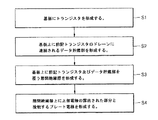
次に、図9に基づいて図1に示した不揮発性メモリ装置の製造方法を説明する。 Next, a method for manufacturing the nonvolatile memory device shown in FIG. 1 will be described with reference to FIG.
図9と共に図1を参照すれば、第1段階S1は、基板40にトランジスタを形成する段階である。第2段階S2は、基板40のドレーン44上に下部電極52、データ貯蔵物質層54、および上部電極56を順次に積層して基板40上に前記トランジスタのドレーン44に連結されるデータ貯蔵部Sを形成する段階である。データ貯蔵物質層54は、印加される電圧によって抵抗が変わる遷移金属酸化膜で形成することが望ましい。例えば、ニッケル酸化膜(NiO)、バナジウム酸化膜(V2O5)、亜鉛酸化膜(ZnO)、ニオブ酸化膜(Nb2O5)、チタン酸化膜(TiO2)、タングステン酸化膜(WO3)、またはコバルト酸化膜(CoO)等で形成する。
Referring to FIG. 1 along with FIG. 9, a first step S1 is a step of forming a transistor on the
第3段階S3は、基板40上に前記トランジスタおよびデータ貯蔵部Sを覆う層間絶縁層60を形成する段階である。第4段階S4は、データ貯蔵部Sの上部電極56を露出させ、層間絶縁層60上に上部電極56の露出された部分と接触するプレート電極58を形成する段階である。データ貯蔵物質層54がニッケル酸化膜で形成された場合、プレート電極58は、基板40上に形成された全てのセル(図示せず)のデータ貯蔵部に含まれている上部電極の全てと接触するプレートパッドで置換えられる。
In the third step S3, an
一方、図3に示したように、データ貯蔵部Sと基板40との間に第1層間絶縁層62を形成し、第1層間絶縁層62にドレーン44が露出されるコンタクトホールh1を形成した後、コンタクトホールh1に導電性プラグ64を充填することができる。次いで、第1層間絶縁層62上に導電性プラグ64と接触するデータ貯蔵部Sを形成できる。
Meanwhile, as shown in FIG. 3, a first
また、下部電極52とデータ貯蔵物質層54をスタックタイプでない立体状に形成してもよい。
Further, the
一方、図面に示されていないが、半導体基板40にダイオードを形成した後、半導体基板40に前記ダイオードと連結されるようにデータ貯蔵部Sを形成できる。この時、データ貯蔵部Sは前記のようなものが望ましい。
Meanwhile, although not shown in the drawings, after the diode is formed on the
前述したように、本発明は、1T−1Rまたは1D−1Rを含む不揮発性メモリ装置においてデータが保存される抵抗体として図4に示した電流−電圧特性を有し、加工が容易な遷移金属酸化膜を備える。したがって、既存のDRAM工程をそのまま使用することができる。これにより、製品の生産性を高め、製品コストを節減することができる。 As described above, the present invention relates to a transition metal which has a current-voltage characteristic shown in FIG. 4 as a resistor for storing data in a nonvolatile memory device including 1T-1R or 1D-1R, and is easy to process. An oxide film is provided. Therefore, the existing DRAM process can be used as it is. Thereby, the productivity of the product can be increased and the product cost can be reduced.
また、抵抗体の抵抗変化を用いてデータを書き込み、読取るために、集積度が高まって抵抗体のサイズが小さくなっても抵抗体のメモリ特性は影響を受けない。また動作特性上、抵抗体に書込まれたデータは非破壊的に読取られるので、データが読取られた後にも前記抵抗体は前記データが読取られる前のデータ状態と同じ状態になり、動作電圧も低くなる。これはデータを読取った後、従来、一般的に行った再貯蔵過程が必要でないことを意味する。 Further, since data is written and read using the resistance change of the resistor, the memory characteristics of the resistor are not affected even if the degree of integration is increased and the size of the resistor is reduced. Also, because of the operating characteristics, the data written in the resistor is read non-destructively, so that even after the data is read, the resistor is in the same data state as before the data was read, and the operating voltage Will also be lower. This means that, after reading the data, the re-storage process conventionally performed generally is not necessary.
前記の説明において、多くの事項が具体的に記載されているが、それらは発明の範囲を限定するものではなく、望ましい実施の形態の例示として解釈しなければならない。例えば、当業者ならば、データ貯蔵物質層54として遷移金属酸化膜の代わりに、データを読取った後にも書込まれたデータが損傷および破壊されない電圧−電流特性を持つ他の物質膜を使用することもできる。したがって、本発明の真の技術的保護範囲は実施の形態により定めてはならず、特許請求の範囲に記載されている技術的思想によってのみ決まるべきである。
In the above description, many items are specifically described, but they do not limit the scope of the invention, and should be construed as exemplifications of preferred embodiments. For example, those skilled in the art will use the data
不揮発性メモリを必要とする全ての電子製品、例えば、コンピュータ、携帯電話、カムコーダ、デジタルカメラ、メモリスティック、またはメモリカード等に使われることができる。 It can be used in all electronic products that require non-volatile memory, such as computers, mobile phones, camcorders, digital cameras, memory sticks, or memory cards.
40…基板、
42…ソース、
44…ドレーン、
46…チャンネル領域、
48…ゲート絶縁膜、
50…ゲート電極、
52…下部電極、
54…データ貯蔵物質層、
56…上部電極、
58…プレート電極、
h1…コンタクタホール、
h2…ビアホール、
D…ダイオード、
S…データ貯蔵部。
40 ... substrate,
42 ... Source,
44 ... Drain,
46 ... channel area,
48 ... Gate insulating film,
50 ... gate electrode,
52 ... lower electrode,
54 ... Data storage material layer
56: upper electrode,
58: plate electrode,
h1… Contactor hole,
h2 ... via hole,
D… Diode,
S: Data storage unit.
Claims (18)
前記基板に形成されたトランジスタと、
前記トランジスタのドレーンに連結されているデータ貯蔵部と、を備え、
前記データ貯蔵部は、異なる電圧で異なる抵抗特性を有するデータ貯蔵物質層を含むことを特徴とする不揮発性メモリ装置。 Board and
A transistor formed on the substrate;
A data storage unit connected to the drain of the transistor,
The nonvolatile memory device according to claim 1, wherein the data storage unit includes a data storage material layer having different resistance characteristics at different voltages.
前記基板に形成されたスイッチング機能を有するダイオードと、
前記ダイオードに連結されているデータ貯蔵部と、を備えることを特徴とする不揮発性メモリ装置。 Board and
A diode having a switching function formed on the substrate;
A data storage unit connected to the diode.
前記基板に形成されたトランジスタおよび前記トランジスタのドレーンに連結されているデータ貯蔵部と、を備える不揮発性メモリ装置の製造方法において、
前記データ貯蔵部は、下部電極、データ貯蔵物質層、および上部電極を順次に積層して形成され、
前記データ貯蔵物質層は、異なる電圧で異なる抵抗特性を有する物質膜で形成されることを特徴とする不揮発性メモリ装置の製造方法。 Board and
A method of manufacturing a nonvolatile memory device, comprising: a transistor formed on the substrate; and a data storage unit connected to a drain of the transistor.
The data storage unit is formed by sequentially stacking a lower electrode, a data storage material layer, and an upper electrode,
The method of manufacturing a nonvolatile memory device, wherein the data storage material layer is formed of material films having different resistance characteristics at different voltages.
前記ダイオードと連結されるようにデータ貯蔵部を形成する段階と、
を含み、
前記データ貯蔵部は、前記ダイオードと連結される下部電極、データ貯蔵物質層、および上部電極を順次に積層して形成することを特徴とする不揮発性メモリ装置の製造方法。 Forming a diode on the substrate;
Forming a data storage unit to be connected to the diode;
Including
The method of manufacturing a nonvolatile memory device, wherein the data storage unit is formed by sequentially stacking a lower electrode, a data storage material layer, and an upper electrode connected to the diode.
Applications Claiming Priority (1)
| Application Number | Priority Date | Filing Date | Title |
|---|---|---|---|
| KR1020030035562A KR100773537B1 (en) | 2003-06-03 | 2003-06-03 | Nonvolatile memory device composing one switching device and one resistant material and method of manufacturing the same |
Publications (3)
| Publication Number | Publication Date |
|---|---|
| JP2004363604A true JP2004363604A (en) | 2004-12-24 |
| JP2004363604A5 JP2004363604A5 (en) | 2008-06-19 |
| JP4511249B2 JP4511249B2 (en) | 2010-07-28 |
Family
ID=33157373
Family Applications (1)
| Application Number | Title | Priority Date | Filing Date |
|---|---|---|---|
| JP2004164659A Active JP4511249B2 (en) | 2003-06-03 | 2004-06-02 | Nonvolatile memory device including one switching element and one resistor, and manufacturing method thereof |
Country Status (6)
| Country | Link |
|---|---|
| US (2) | US8164130B2 (en) |
| EP (3) | EP2164104A3 (en) |
| JP (1) | JP4511249B2 (en) |
| KR (1) | KR100773537B1 (en) |
| CN (2) | CN1574363B (en) |
| DE (1) | DE602004025877D1 (en) |
Cited By (71)
| Publication number | Priority date | Publication date | Assignee | Title |
|---|---|---|---|---|
| JP2006140464A (en) * | 2004-11-10 | 2006-06-01 | Samsung Electronics Co Ltd | Intersection point nonvolatile memory element using two-component system metal oxide film as data storage substance film, and method of manufacturing the same |
| JP2006210882A (en) * | 2005-01-31 | 2006-08-10 | Samsung Electronics Co Ltd | Nonvolatile memory element using resistor and its manufacturing method |
| JP2006319342A (en) * | 2005-05-12 | 2006-11-24 | Samsung Electronics Co Ltd | Transistor using metal-insulator transition material, and method of manufacturing the same |
| JP2006344875A (en) * | 2005-06-10 | 2006-12-21 | Sharp Corp | Method of manufacturing variable resistive element |
| JP2007005609A (en) * | 2005-06-24 | 2007-01-11 | Sharp Corp | Memory cell, semiconductor device and manufacturing method therefor |
| JP2007012035A (en) * | 2005-05-31 | 2007-01-18 | Semiconductor Energy Lab Co Ltd | Semiconductor device |
| WO2007020832A1 (en) * | 2005-08-15 | 2007-02-22 | National Institute Of Advanced Industrial Science And Technology | Switching device |
| JP2007073950A (en) * | 2005-08-12 | 2007-03-22 | Semiconductor Energy Lab Co Ltd | Semiconductor device and method of fabricating the same |
| WO2007074642A1 (en) * | 2005-12-27 | 2007-07-05 | Sharp Kabushiki Kaisha | Variable resistance element, its fabrication method, and semiconductor storage device using the same |
| WO2007125674A1 (en) * | 2006-04-28 | 2007-11-08 | Sharp Kabushiki Kaisha | Variable resistance element, and its manufacturing method |
| JP2007294998A (en) * | 2005-12-02 | 2007-11-08 | Sharp Corp | Variable resistive element and its manufacturing method |
| JP2007294925A (en) * | 2006-04-21 | 2007-11-08 | Samsung Electronics Co Ltd | Nonvolatile memory element, operation method therefor, and manufacturing method therefor |
| JP2008016854A (en) * | 2006-07-06 | 2008-01-24 | Samsung Electronics Co Ltd | Nonvolatile memory element containing variable resistive material |
| JP2008034434A (en) * | 2006-07-26 | 2008-02-14 | National Institute Of Advanced Industrial & Technology | Switching element, and manufacturing method thereof |
| JP2008091747A (en) * | 2006-10-04 | 2008-04-17 | Seiko Epson Corp | Variable resistive element |
| WO2008059701A1 (en) | 2006-11-17 | 2008-05-22 | Panasonic Corporation | Nonvolatile memory element, nonvolatile memory device, nonvolatile semiconductor device, and method for manufacturing nonvolatile memory element |
| JP2008124471A (en) * | 2006-11-09 | 2008-05-29 | Samsung Electronics Co Ltd | Nonvolatile storage device, and its operation method |
| WO2008068800A1 (en) * | 2006-11-30 | 2008-06-12 | Fujitsu Limited | Resistance storage element, method for fabricating the same, and nonvolatile semiconductor storage device |
| WO2008075471A1 (en) * | 2006-12-19 | 2008-06-26 | Fujitsu Limited | Resistance change element and method for manufacturing the same |
| WO2008075413A1 (en) * | 2006-12-19 | 2008-06-26 | Fujitsu Limited | Resistance change device and process for producing the same |
| WO2008075414A1 (en) * | 2006-12-19 | 2008-06-26 | Fujitsu Limited | Process for producing resistance change device |
| JP2008182156A (en) * | 2007-01-26 | 2008-08-07 | Nippon Telegr & Teleph Corp <Ntt> | Metal oxide element and its fabrication process |
| JP2008182154A (en) * | 2007-01-26 | 2008-08-07 | Nippon Telegr & Teleph Corp <Ntt> | Memory device |
| WO2008117371A1 (en) * | 2007-03-23 | 2008-10-02 | Fujitsu Limited | Resistance storage element and non-volatile semiconductor storage device |
| WO2008132899A1 (en) * | 2007-04-17 | 2008-11-06 | Nec Corporation | Resistance change element and semiconductor device including it |
| JP2008541452A (en) * | 2005-05-09 | 2008-11-20 | サンディスク スリーディー,エルエルシー | Nonvolatile memory cell with diode and resistivity switching material |
| WO2008149484A1 (en) | 2007-06-05 | 2008-12-11 | Panasonic Corporation | Nonvolatile storage element, its manufacturing method, and nonvolatile semiconductor device using the nonvolatile storage element |
| JP2009500844A (en) * | 2005-06-30 | 2009-01-08 | エレクトロニクス アンド テレコミュニケーションズ リサーチ インスチチュート | Memory device using abrupt metal-insulator transition and operation method thereof |
| JP2009500845A (en) * | 2005-07-04 | 2009-01-08 | インダストリー ユニバーシティー コーポレーション ファウンデーション ハンヤン ユニバーシティー | Method for forming multilayer binary oxide film for ReRAM |
| JP2009505424A (en) * | 2005-08-15 | 2009-02-05 | マイクロン テクノロジー, インク. | Reproducible variable resistance insulated memory device and method of forming the same |
| WO2009022693A1 (en) * | 2007-08-15 | 2009-02-19 | Sony Corporation | Storage device drive method |
| JP2009518861A (en) * | 2005-12-09 | 2009-05-07 | サンディスク スリーディー,エルエルシー | Deposited semiconductor structure and fabrication method for minimizing n-type dopant diffusion |
| WO2009142165A1 (en) * | 2008-05-20 | 2009-11-26 | 日本電気株式会社 | Semiconductor device and method for fabricating the same |
| US7692178B2 (en) | 2006-03-08 | 2010-04-06 | Panasonic Corporation | Nonvolatile memory element, nonvolatile memory apparatus, and method of manufacture thereof |
| JP2010103555A (en) * | 2009-12-25 | 2010-05-06 | Sharp Corp | Variable resistor element |
| JP2010521062A (en) * | 2007-03-01 | 2010-06-17 | サンディスク スリーディー,エルエルシー | Method for plasma etching transition metal oxides |
| US7781230B2 (en) | 2006-04-13 | 2010-08-24 | Panasonic Corporation | Electro-resistance element, electro-resistance memory using the same and method of manufacturing the same |
| US7791119B2 (en) | 2006-04-19 | 2010-09-07 | Panasonic Corporation | Electro-resistance element and electro-resistance memory using the same |
| JP2010532569A (en) * | 2007-06-29 | 2010-10-07 | サンディスク スリーディー,エルエルシー | Memory cell using reversible resistance switching element by selective attachment and method of forming the same |
| JP2010251529A (en) * | 2009-04-16 | 2010-11-04 | Sony Corp | Semiconductor memory device and method of manufacturing the same |
| US7894239B2 (en) | 2007-12-07 | 2011-02-22 | Sharp Kabushiki Kaisha | Variable resistance element, method for producing the same, and nonvolatile semiconductor storage device |
| US7915656B2 (en) | 2006-10-24 | 2011-03-29 | Panasonic Corporation | Nonvolatile semiconductor memory apparatus and manufacturing method thereof |
| US7924138B2 (en) | 2007-03-01 | 2011-04-12 | Fujitsu Limited | Semiconductor device and manufacturing method of the same |
| US7948789B2 (en) | 2007-04-09 | 2011-05-24 | Panasonic Corporation | Resistance variable element, nonvolatile switching element, and resistance variable memory apparatus |
| US7964869B2 (en) | 2006-08-25 | 2011-06-21 | Panasonic Corporation | Memory element, memory apparatus, and semiconductor integrated circuit |
| WO2011080866A1 (en) * | 2009-12-28 | 2011-07-07 | パナソニック株式会社 | Memory device and manufacturing method therefor |
| US8018761B2 (en) | 2006-12-28 | 2011-09-13 | Panasonic Corporation | Resistance variable element, resistance variable memory apparatus, and resistance variable apparatus |
| US8018760B2 (en) | 2006-12-28 | 2011-09-13 | Panasonic Corporation | Resistance variable element and resistance variable memory apparatus |
| US8054674B2 (en) | 2007-05-10 | 2011-11-08 | Sharp Kabushiki Kaisha | Variable resistive element, manufacturing method for same, and non-volatile semiconductor memory device |
| US8058636B2 (en) | 2007-03-29 | 2011-11-15 | Panasonic Corporation | Variable resistance nonvolatile memory apparatus |
| US8125818B2 (en) | 2008-02-25 | 2012-02-28 | Panasonic Corporation | Method of programming variable resistance element and variable resistance memory device using the same |
| US8148711B2 (en) | 2007-05-18 | 2012-04-03 | Panasonic Corporation | Nonvolatile memory element, manufacturing method thereof, and nonvolatile semiconductor apparatus using nonvolatile memory element |
| US8253136B2 (en) | 2007-10-30 | 2012-08-28 | Panasonic Corporation | Nonvolatile semiconductor memory device and manufacturing method thereof |
| US8258493B2 (en) | 2006-11-20 | 2012-09-04 | Panasonic Corporation | Nonvolatile semiconductor memory apparatus and manufacturing method thereof |
| US8264865B2 (en) | 2008-07-11 | 2012-09-11 | Panasonic Corporation | Nonvolatile memory element, manufacturing method thereof, and nonvolatile semiconductor device incorporating nonvolatile memory element |
| US8279658B2 (en) | 2009-03-25 | 2012-10-02 | Panasonic Corporation | Method of programming variable resistance element and nonvolatile storage device |
| US8279657B2 (en) | 2008-12-04 | 2012-10-02 | Panasonic Corporation | Nonvolatile memory element and nonvolatile memory device |
| US8309946B2 (en) | 2009-01-29 | 2012-11-13 | Panasonic Corporation | Resistance variable element |
| US8331136B2 (en) | 2009-06-25 | 2012-12-11 | Sony Corporation | Recording method of nonvolatile memory and nonvolatile memory |
| US8345465B2 (en) | 2008-09-30 | 2013-01-01 | Panasonic Corporation | Driving method of variable resistance element, initialization method of variable resistance element, and nonvolatile storage device |
| US8405076B2 (en) | 2009-02-04 | 2013-03-26 | Panasonic Corporation | Nonvolatile memory element |
| US8432721B2 (en) | 2010-02-02 | 2013-04-30 | Panasonic Corporation | Method of programming variable resistance element, method of initializing variable resistance element, and nonvolatile storage device |
| US8441060B2 (en) | 2008-10-01 | 2013-05-14 | Panasonic Corporation | Nonvolatile memory element and nonvolatile memory device incorporating nonvolatile memory element |
| US8450145B2 (en) | 2009-12-16 | 2013-05-28 | Sharp Kabushiki Kaisha | Nonvolatile semiconductor memory device and method for producing the same |
| US8482953B2 (en) | 2009-03-12 | 2013-07-09 | Fujitsu Limited | Composite resistance variable element and method for manufacturing the same |
| US8536067B2 (en) | 2005-08-12 | 2013-09-17 | Semiconductor Energy Laboratory Co., Ltd. | Semiconductor device and method for manufacturing the same |
| US9111610B2 (en) | 2012-04-20 | 2015-08-18 | Panasonic Intellectual Property Management Co., Ltd. | Method of driving nonvolatile memory element and nonvolatile memory device |
| US9142289B2 (en) | 2011-06-13 | 2015-09-22 | Panasonic Intellectual Property Management Co., Ltd. | Method for driving variable resistance element, and nonvolatile memory device |
| US9153319B2 (en) | 2011-03-14 | 2015-10-06 | Panasonic Intellectual Property Management Co., Ltd. | Method for driving nonvolatile memory element, and nonvolatile memory device having a variable resistance element |
| US10490276B2 (en) | 2017-09-12 | 2019-11-26 | Panasonic Corporation | Non-volatile storage device and driving method |
| US11889776B2 (en) | 2018-12-26 | 2024-01-30 | Nuvoton Technology Corporation Japan | Variable resistance non-volatile memory element and variable resistance non-volatile memory device using the element |
Families Citing this family (106)
| Publication number | Priority date | Publication date | Assignee | Title |
|---|---|---|---|---|
| JP5792918B2 (en) * | 2000-08-14 | 2015-10-14 | サンディスク・スリー・ディ・リミテッド・ライアビリティ・カンパニーSandisk 3D Llc | Highly integrated memory device |
| DE10255117A1 (en) * | 2002-11-26 | 2004-06-17 | Infineon Technologies Ag | Semiconductor memory device and method for its production |
| KR100773537B1 (en) | 2003-06-03 | 2007-11-07 | 삼성전자주식회사 | Nonvolatile memory device composing one switching device and one resistant material and method of manufacturing the same |
| KR101051704B1 (en) * | 2004-04-28 | 2011-07-25 | 삼성전자주식회사 | Memory device using multilayer with resistive gradient |
| FR2887149B1 (en) * | 2005-06-17 | 2007-08-03 | Galderma Sa | PROCESS FOR SOLUBILIZING THE METRONIDAZOLE |
| KR100593448B1 (en) * | 2004-09-10 | 2006-06-28 | 삼성전자주식회사 | Non-volatile memory cells employing a transition metal oxide layer as a data storage material layer and methods of fabricating the same |
| KR100738070B1 (en) * | 2004-11-06 | 2007-07-12 | 삼성전자주식회사 | Nonvolitile Memory Device Comprising One Resistance Material and One Transistor |
| KR100657911B1 (en) * | 2004-11-10 | 2006-12-14 | 삼성전자주식회사 | Nonvolitile Memory Device Comprising One Resistance Material and One Diode |
| KR100576369B1 (en) * | 2004-11-23 | 2006-05-03 | 삼성전자주식회사 | Method for programming a non-volatile memory device employing a transition metal oxide layer as a data storage material layer |
| KR100682908B1 (en) * | 2004-12-21 | 2007-02-15 | 삼성전자주식회사 | Nonvolitile memory device comprising two resistance material layer |
| KR100693409B1 (en) * | 2005-01-14 | 2007-03-12 | 광주과학기술원 | Nonvolatile Memory Device Based on Resistance Switching of Oxide ? Method Thereof |
| KR100657956B1 (en) | 2005-04-06 | 2006-12-14 | 삼성전자주식회사 | Multi-bit memory device having resistive material layers as storage node and methods of manufacturing and operating the same |
| US20060273298A1 (en) * | 2005-06-02 | 2006-12-07 | Matrix Semiconductor, Inc. | Rewriteable memory cell comprising a transistor and resistance-switching material in series |
| JP3889023B2 (en) * | 2005-08-05 | 2007-03-07 | シャープ株式会社 | Variable resistance element, method for manufacturing the same, and memory device including the same |
| KR101100427B1 (en) * | 2005-08-24 | 2011-12-30 | 삼성전자주식회사 | Nonvolatile semiconductor memory device comprising ion conducting layer and methods of manufacturing and operating the same |
| US7601995B2 (en) * | 2005-10-27 | 2009-10-13 | Infineon Technologies Ag | Integrated circuit having resistive memory cells |
| US8222917B2 (en) * | 2005-11-03 | 2012-07-17 | Agate Logic, Inc. | Impedance matching and trimming apparatuses and methods using programmable resistance devices |
| KR100668348B1 (en) | 2005-11-11 | 2007-01-12 | 삼성전자주식회사 | Nonvolatile memory device and fabrication method of the same |
| US7834338B2 (en) * | 2005-11-23 | 2010-11-16 | Sandisk 3D Llc | Memory cell comprising nickel-cobalt oxide switching element |
| US7816659B2 (en) * | 2005-11-23 | 2010-10-19 | Sandisk 3D Llc | Devices having reversible resistivity-switching metal oxide or nitride layer with added metal |
| JP4061328B2 (en) * | 2005-12-02 | 2008-03-19 | シャープ株式会社 | Variable resistance element and manufacturing method thereof |
| KR100684908B1 (en) | 2006-01-09 | 2007-02-22 | 삼성전자주식회사 | Multi-resistive state memory element, memory cell, operating thereof, and data processing system using the memory element |
| US7714315B2 (en) | 2006-02-07 | 2010-05-11 | Qimonda North America Corp. | Thermal isolation of phase change memory cells |
| KR100718155B1 (en) * | 2006-02-27 | 2007-05-14 | 삼성전자주식회사 | Non-volatile memory device using two oxide layer |
| KR101176543B1 (en) * | 2006-03-10 | 2012-08-28 | 삼성전자주식회사 | Resistance Random Memory Device |
| US7808810B2 (en) | 2006-03-31 | 2010-10-05 | Sandisk 3D Llc | Multilevel nonvolatile memory cell comprising a resistivity-switching oxide or nitride and an antifuse |
| US7875871B2 (en) | 2006-03-31 | 2011-01-25 | Sandisk 3D Llc | Heterojunction device comprising a semiconductor and a resistivity-switching oxide or nitride |
| TWI462099B (en) * | 2006-03-31 | 2014-11-21 | Sandisk 3D Llc | Nonvolatile memory cells, monolithic three dimensional memory arrays and methods for programming such memory arrays |
| US7829875B2 (en) | 2006-03-31 | 2010-11-09 | Sandisk 3D Llc | Nonvolatile rewritable memory cell comprising a resistivity-switching oxide or nitride and an antifuse |
| KR101239962B1 (en) | 2006-05-04 | 2013-03-06 | 삼성전자주식회사 | Variable resistive memory device comprising buffer layer on lower electrode |
| US20070267621A1 (en) * | 2006-05-19 | 2007-11-22 | Infineon Technologies Ag | Resistive memory device |
| KR101206034B1 (en) * | 2006-05-19 | 2012-11-28 | 삼성전자주식회사 | Nonvolatile memory device using oxygen-deficient metal oxide layer and the fabrication method |
| KR100818271B1 (en) * | 2006-06-27 | 2008-03-31 | 삼성전자주식회사 | Threshold switching operation method of nonvolitile memory device induced by pulse voltage |
| US8232175B2 (en) | 2006-09-14 | 2012-07-31 | Spansion Llc | Damascene metal-insulator-metal (MIM) device with improved scaleability |
| CN101174672A (en) | 2006-10-04 | 2008-05-07 | 旺宏电子股份有限公司 | Storage cell and its manufacturing process |
| US7524722B2 (en) | 2006-10-12 | 2009-04-28 | Macronix International Co., Ltd. | Resistance type memory device and fabricating method and operating method thereof |
| KR101133832B1 (en) * | 2006-11-08 | 2012-04-06 | 시메트릭스 주식회사 | Correlated electron memory |
| KR101206036B1 (en) | 2006-11-16 | 2012-11-28 | 삼성전자주식회사 | Resistive random access memory enclosing a transition metal solid solution and Manufacturing Method for the same |
| KR100846502B1 (en) * | 2006-11-21 | 2008-07-17 | 삼성전자주식회사 | Nonvolatile memory device and method of fabricating the same |
| KR100982424B1 (en) * | 2006-11-28 | 2010-09-15 | 삼성전자주식회사 | Manufacturing Method for the Resistive random access memory device |
| KR20080064353A (en) * | 2007-01-04 | 2008-07-09 | 삼성전자주식회사 | Resistive random access memory and manufacturing method for the same |
| US7704789B2 (en) | 2007-02-05 | 2010-04-27 | Intermolecular, Inc. | Methods for forming resistive switching memory elements |
| US7678607B2 (en) * | 2007-02-05 | 2010-03-16 | Intermolecular, Inc. | Methods for forming resistive switching memory elements |
| US7972897B2 (en) | 2007-02-05 | 2011-07-05 | Intermolecular, Inc. | Methods for forming resistive switching memory elements |
| WO2008097742A1 (en) * | 2007-02-05 | 2008-08-14 | Interolecular, Inc. | Methods for forming resistive switching memory elements |
| US7629198B2 (en) | 2007-03-05 | 2009-12-08 | Intermolecular, Inc. | Methods for forming nonvolatile memory elements with resistive-switching metal oxides |
| US8097878B2 (en) | 2007-03-05 | 2012-01-17 | Intermolecular, Inc. | Nonvolatile memory elements with metal-deficient resistive-switching metal oxides |
| US7960224B2 (en) | 2007-04-03 | 2011-06-14 | Macronix International Co., Ltd. | Operation method for multi-level switching of metal-oxide based RRAM |
| WO2008140979A1 (en) | 2007-05-09 | 2008-11-20 | Intermolecular, Inc. | Resistive-switching nonvolatile memory elements |
| KR101350979B1 (en) | 2007-05-11 | 2014-01-14 | 삼성전자주식회사 | Resistive memory device and Manufacturing Method for the same |
| US8173989B2 (en) * | 2007-05-30 | 2012-05-08 | Samsung Electronics Co., Ltd. | Resistive random access memory device and methods of manufacturing and operating the same |
| US7846785B2 (en) | 2007-06-29 | 2010-12-07 | Sandisk 3D Llc | Memory cell that employs a selectively deposited reversible resistance-switching element and methods of forming the same |
| US7902537B2 (en) | 2007-06-29 | 2011-03-08 | Sandisk 3D Llc | Memory cell that employs a selectively grown reversible resistance-switching element and methods of forming the same |
| US8233308B2 (en) | 2007-06-29 | 2012-07-31 | Sandisk 3D Llc | Memory cell that employs a selectively deposited reversible resistance-switching element and methods of forming the same |
| US7824956B2 (en) | 2007-06-29 | 2010-11-02 | Sandisk 3D Llc | Memory cell that employs a selectively grown reversible resistance-switching element and methods of forming the same |
| TWI402980B (en) | 2007-07-20 | 2013-07-21 | Macronix Int Co Ltd | Resistive memory structure with buffer layer |
| KR101482814B1 (en) | 2007-07-25 | 2015-01-14 | 인터몰레큘러 인코퍼레이티드 | Multistate nonvolatile memory elements |
| WO2009015298A2 (en) | 2007-07-25 | 2009-01-29 | Intermolecular, Inc. | Nonvolatile memory elements |
| US8338816B2 (en) * | 2007-10-15 | 2012-12-25 | Panasonic Corporation | Nonvolatile memory element, and nonvolatile semiconductor device using the nonvolatile memory element |
| US8345462B2 (en) | 2007-12-05 | 2013-01-01 | Macronix International Co., Ltd. | Resistive memory and method for manufacturing the same |
| US7759201B2 (en) * | 2007-12-17 | 2010-07-20 | Sandisk 3D Llc | Method for fabricating pitch-doubling pillar structures |
| US7706169B2 (en) * | 2007-12-27 | 2010-04-27 | Sandisk 3D Llc | Large capacity one-time programmable memory cell using metal oxides |
| US7764534B2 (en) * | 2007-12-28 | 2010-07-27 | Sandisk 3D Llc | Two terminal nonvolatile memory using gate controlled diode elements |
| JP4549401B2 (en) * | 2008-03-11 | 2010-09-22 | 富士通株式会社 | Manufacturing method of resistance memory element |
| JP5488458B2 (en) * | 2008-04-07 | 2014-05-14 | 日本電気株式会社 | Resistance change element and manufacturing method thereof |
| US7981592B2 (en) * | 2008-04-11 | 2011-07-19 | Sandisk 3D Llc | Double patterning method |
| US7786015B2 (en) * | 2008-04-28 | 2010-08-31 | Sandisk 3D Llc | Method for fabricating self-aligned complementary pillar structures and wiring |
| US7781269B2 (en) * | 2008-06-30 | 2010-08-24 | Sandisk 3D Llc | Triangle two dimensional complementary patterning of pillars |
| US7732235B2 (en) | 2008-06-30 | 2010-06-08 | Sandisk 3D Llc | Method for fabricating high density pillar structures by double patterning using positive photoresist |
| US7981742B2 (en) * | 2008-07-02 | 2011-07-19 | Macronic International Co., Ltd. | Semiconductor device, data element thereof and method of fabricating the same |
| US8076056B2 (en) * | 2008-10-06 | 2011-12-13 | Sandisk 3D Llc | Method of making sub-resolution pillar structures using undercutting technique |
| KR20100041155A (en) | 2008-10-13 | 2010-04-22 | 삼성전자주식회사 | Resistive memory device |
| US8080443B2 (en) * | 2008-10-27 | 2011-12-20 | Sandisk 3D Llc | Method of making pillars using photoresist spacer mask |
| US8114765B2 (en) | 2008-12-31 | 2012-02-14 | Sandisk 3D Llc | Methods for increased array feature density |
| US8084347B2 (en) | 2008-12-31 | 2011-12-27 | Sandisk 3D Llc | Resist feature and removable spacer pitch doubling patterning method for pillar structures |
| US7846756B2 (en) * | 2008-12-31 | 2010-12-07 | Sandisk 3D Llc | Nanoimprint enhanced resist spacer patterning method |
| JP2010177624A (en) * | 2009-02-02 | 2010-08-12 | Toshiba Corp | Semiconductor storage device |
| US8445886B2 (en) | 2009-02-02 | 2013-05-21 | Panasonic Corporation | Nonvolatile memory element, nonvolatile memory device, nonvolatile semiconductor device, and method of manufacturing nonvolatile memory element |
| US8488362B2 (en) * | 2009-04-29 | 2013-07-16 | Macronix International Co., Ltd. | Graded metal oxide resistance based semiconductor memory device |
| KR20110072921A (en) | 2009-12-23 | 2011-06-29 | 삼성전자주식회사 | Memory device and method of operating the same |
| KR20110074354A (en) | 2009-12-24 | 2011-06-30 | 삼성전자주식회사 | Memory device and method of operating the same |
| US8026178B2 (en) | 2010-01-12 | 2011-09-27 | Sandisk 3D Llc | Patterning method for high density pillar structures |
| US7923305B1 (en) | 2010-01-12 | 2011-04-12 | Sandisk 3D Llc | Patterning method for high density pillar structures |
| KR20110101983A (en) | 2010-03-10 | 2011-09-16 | 삼성전자주식회사 | Bipolar memory cell and memory device including the same |
| WO2012005003A1 (en) | 2010-07-08 | 2012-01-12 | パナソニック株式会社 | Nonvolatile semiconductor memory device and method for fabricating same |
| US8264868B2 (en) | 2010-10-25 | 2012-09-11 | Hewlett-Packard Development Company, L.P. | Memory array with metal-insulator transition switching devices |
| CN102064276B (en) * | 2010-11-01 | 2014-06-04 | 华中科技大学 | Asymmetric phase-change memory unit and element |
| US8699258B2 (en) | 2011-01-21 | 2014-04-15 | Macronix International Co., Ltd. | Verification algorithm for metal-oxide resistive memory |
| US8951829B2 (en) | 2011-04-01 | 2015-02-10 | Micron Technology, Inc. | Resistive switching in memory cells |
| JP2014032724A (en) * | 2012-08-03 | 2014-02-20 | Sharp Corp | Semiconductor storage device |
| US9231204B2 (en) * | 2012-09-28 | 2016-01-05 | Intel Corporation | Low voltage embedded memory having conductive oxide and electrode stacks |
| TWI513074B (en) * | 2013-01-08 | 2015-12-11 | Nat Univ Tsing Hua | Resistive random access memory |
| JP5830655B2 (en) | 2013-04-30 | 2015-12-09 | パナソニックIpマネジメント株式会社 | Method for driving nonvolatile memory element |
| CN103367639B (en) * | 2013-07-25 | 2015-09-09 | 福州大学 | A kind of Zinc oxide nanowire low-power consumption resistance-variable storing device and preparation method thereof |
| CN103682100B (en) * | 2013-12-06 | 2016-04-06 | 南昌大学 | The data storage of zinc oxide/polymethyl methacrylate/cuprous sulfocyanide structure and preparation method |
| CN103985816B (en) * | 2014-05-28 | 2016-09-14 | 淮阴师范学院 | A kind of aluminum/Fe2O3 doping amorphous carbon-film/aluminum nano thin-film memory resistor memory device and preparation method thereof |
| TWI548127B (en) * | 2014-09-19 | 2016-09-01 | 華邦電子股份有限公司 | Resistive random access memory |
| CN105448948B (en) * | 2014-09-30 | 2019-01-11 | 华邦电子股份有限公司 | Resistive random access memory |
| US10355205B2 (en) | 2014-12-18 | 2019-07-16 | Intel Corporation | Resistive memory cells including localized filamentary channels, devices including the same, and methods of making the same |
| US20170117464A1 (en) * | 2015-10-22 | 2017-04-27 | Winbond Electronics Corp. | Resistive random access memory device |
| CN109698213A (en) * | 2017-10-20 | 2019-04-30 | 联华电子股份有限公司 | Semiconductor structure and preparation method thereof |
| US11424407B2 (en) * | 2020-09-02 | 2022-08-23 | Winbond Electronics Corp. | Resistive random access memory and method of manufacturing the same |
| US11469373B2 (en) * | 2020-09-10 | 2022-10-11 | Rockwell Collins, Inc. | System and device including memristor material |
| US11631808B2 (en) | 2020-12-07 | 2023-04-18 | Rockwell Collins, Inc. | System and device including memristor material |
| US11462267B2 (en) | 2020-12-07 | 2022-10-04 | Rockwell Collins, Inc. | System and device including memristor material |
| US11456418B2 (en) | 2020-09-10 | 2022-09-27 | Rockwell Collins, Inc. | System and device including memristor materials in parallel |
Citations (4)
| Publication number | Priority date | Publication date | Assignee | Title |
|---|---|---|---|---|
| JPH0258264A (en) * | 1988-08-23 | 1990-02-27 | Matsushita Electric Ind Co Ltd | Memory device |
| JPH06509909A (en) * | 1991-08-19 | 1994-11-02 | エナージー・コンバーション・デバイセス・インコーポレーテッド | Electrically Erasable Directly Overwritable Multi-Bit Single Cell Memory Devices and Arrays Made Therefrom |
| JP2002537627A (en) * | 1999-02-17 | 2002-11-05 | インターナショナル・ビジネス・マシーンズ・コーポレーション | Microelectronic device for storing information and method thereof |
| WO2003028124A1 (en) * | 2001-09-25 | 2003-04-03 | Japan Science And Technology Agency | Electric device comprising solid electrolyte |
Family Cites Families (50)
| Publication number | Priority date | Publication date | Assignee | Title |
|---|---|---|---|---|
| US3761896A (en) * | 1972-04-18 | 1973-09-25 | Ibm | Memory array of cells containing bistable switchable resistors |
| US4472296A (en) * | 1982-06-21 | 1984-09-18 | Iowa State University Research Foundation, Inc. | Bulk, polycrystalline switching materials for threshold and/or memory switching |
| JPS6242582A (en) | 1985-08-20 | 1987-02-24 | Matsushita Electric Ind Co Ltd | Nonlinear resistance element and manufacture of same |
| JPS63226981A (en) | 1987-03-16 | 1988-09-21 | Fujitsu Ltd | Superconducting integrated circuit device and its manufacture |
| FR2636481B1 (en) * | 1988-09-14 | 1990-11-30 | Sgs Thomson Microelectronics | INTEGRATED ACTIVE LED |
| US5406509A (en) | 1991-01-18 | 1995-04-11 | Energy Conversion Devices, Inc. | Electrically erasable, directly overwritable, multibit single cell memory elements and arrays fabricated therefrom |
| KR970009616B1 (en) * | 1993-12-31 | 1997-06-14 | Hyundai Electronics Ind | Fabricating method of semiconductor device |
| US5751012A (en) * | 1995-06-07 | 1998-05-12 | Micron Technology, Inc. | Polysilicon pillar diode for use in a non-volatile memory cell |
| US5640343A (en) * | 1996-03-18 | 1997-06-17 | International Business Machines Corporation | Magnetic memory array using magnetic tunnel junction devices in the memory cells |
| US6461982B2 (en) * | 1997-02-27 | 2002-10-08 | Micron Technology, Inc. | Methods for forming a dielectric film |
| JP3236262B2 (en) * | 1998-06-16 | 2001-12-10 | 松下電器産業株式会社 | Ferroelectric memory device |
| US6586790B2 (en) * | 1998-07-24 | 2003-07-01 | Kabushiki Kaisha Toshiba | Semiconductor device and method for manufacturing the same |
| GB9902993D0 (en) | 1999-02-11 | 1999-03-31 | Univ Strathclyde | Low pressure chemical vapour deposition of titanium dioxide |
| US6151241A (en) * | 1999-05-19 | 2000-11-21 | Symetrix Corporation | Ferroelectric memory with disturb protection |
| US6297539B1 (en) | 1999-07-19 | 2001-10-02 | Sharp Laboratories Of America, Inc. | Doped zirconia, or zirconia-like, dielectric film transistor structure and deposition method for same |
| JP2001148465A (en) * | 1999-11-18 | 2001-05-29 | Nec Corp | Method of manufacturing semiconductor device |
| WO2001088972A1 (en) * | 2000-05-15 | 2001-11-22 | Asm Microchemistry Oy | Process for producing integrated circuits |
| US20020036313A1 (en) * | 2000-06-06 | 2002-03-28 | Sam Yang | Memory cell capacitor structure and method of formation |
| US6605311B2 (en) * | 2000-06-22 | 2003-08-12 | The Procter & Gamble Company | Insoluble protein particles |
| JP4050446B2 (en) * | 2000-06-30 | 2008-02-20 | 株式会社東芝 | Solid state magnetic memory |
| JP2002176150A (en) * | 2000-09-27 | 2002-06-21 | Canon Inc | Nonvolatile solid-state memory element utilizing magnetoresistance effect, memory, and its recording/ reproducing method |
| JP4223189B2 (en) * | 2000-12-26 | 2009-02-12 | 富士通マイクロエレクトロニクス株式会社 | Semiconductor device and manufacturing method thereof |
| US6358756B1 (en) * | 2001-02-07 | 2002-03-19 | Micron Technology, Inc. | Self-aligned, magnetoresistive random-access memory (MRAM) structure utilizing a spacer containment scheme |
| JP3892736B2 (en) * | 2001-03-29 | 2007-03-14 | 株式会社東芝 | Semiconductor memory device |
| DE10128482A1 (en) * | 2001-06-12 | 2003-01-02 | Infineon Technologies Ag | Production of a semiconductor memory comprises forming edge regions in an insulating region using a spacer element after forming the recess to expose the surface region of an access electrode arrangement |
| US7135734B2 (en) * | 2001-08-30 | 2006-11-14 | Micron Technology, Inc. | Graded composition metal oxide tunnel barrier interpoly insulators |
| US6773929B2 (en) * | 2001-09-14 | 2004-08-10 | Hynix Semiconductor Inc. | Ferroelectric memory device and method for manufacturing the same |
| KR20030034500A (en) * | 2001-10-23 | 2003-05-09 | 주식회사 하이닉스반도체 | Magnetic random access memory |
| EP1326254B1 (en) * | 2001-12-27 | 2009-02-25 | STMicroelectronics S.r.l. | Architecture of a phase-change nonvolatile memory array |
| US6667900B2 (en) * | 2001-12-28 | 2003-12-23 | Ovonyx, Inc. | Method and apparatus to operate a memory cell |
| US6891749B2 (en) * | 2002-02-20 | 2005-05-10 | Micron Technology, Inc. | Resistance variable ‘on ’ memory |
| US6847535B2 (en) * | 2002-02-20 | 2005-01-25 | Micron Technology, Inc. | Removable programmable conductor memory card and associated read/write device and method of operation |
| WO2003079463A2 (en) * | 2002-03-15 | 2003-09-25 | Axon Technologies Corporation | Programmable structure, an array including the structure, and methods of forming the same |
| US20030189851A1 (en) | 2002-04-09 | 2003-10-09 | Brandenberger Sarah M. | Non-volatile, multi-level memory device |
| JP4103497B2 (en) * | 2002-04-18 | 2008-06-18 | ソニー株式会社 | Memory device and method for manufacturing and using the same, semiconductor device and method for manufacturing the same |
| US6850432B2 (en) * | 2002-08-20 | 2005-02-01 | Macronix International Co., Ltd. | Laser programmable electrically readable phase-change memory method and device |
| US6583003B1 (en) * | 2002-09-26 | 2003-06-24 | Sharp Laboratories Of America, Inc. | Method of fabricating 1T1R resistive memory array |
| US6795338B2 (en) * | 2002-12-13 | 2004-09-21 | Intel Corporation | Memory having access devices using phase change material such as chalcogenide |
| US7589343B2 (en) * | 2002-12-13 | 2009-09-15 | Intel Corporation | Memory and access device and method therefor |
| US7205562B2 (en) * | 2002-12-13 | 2007-04-17 | Intel Corporation | Phase change memory and method therefor |
| US6887523B2 (en) | 2002-12-20 | 2005-05-03 | Sharp Laboratories Of America, Inc. | Method for metal oxide thin film deposition via MOCVD |
| US7042052B2 (en) * | 2003-02-10 | 2006-05-09 | Micron Technology, Inc. | Transistor constructions and electronic devices |
| KR100773537B1 (en) | 2003-06-03 | 2007-11-07 | 삼성전자주식회사 | Nonvolatile memory device composing one switching device and one resistant material and method of manufacturing the same |
| KR101051704B1 (en) * | 2004-04-28 | 2011-07-25 | 삼성전자주식회사 | Memory device using multilayer with resistive gradient |
| KR100651656B1 (en) * | 2004-11-29 | 2006-12-01 | 한국과학기술연구원 | Phase change memory cell with transparent conducting oxide for electrode contact material |
| KR100585175B1 (en) * | 2005-01-31 | 2006-05-30 | 삼성전자주식회사 | Fabrication method of gesbte thin film by chemical vapor deposition process |
| US20070132049A1 (en) * | 2005-12-12 | 2007-06-14 | Stipe Barry C | Unipolar resistance random access memory (RRAM) device and vertically stacked architecture |
| KR100718155B1 (en) * | 2006-02-27 | 2007-05-14 | 삼성전자주식회사 | Non-volatile memory device using two oxide layer |
| KR101054321B1 (en) * | 2007-03-01 | 2011-08-05 | 후지쯔 가부시끼가이샤 | Semiconductor device and manufacturing method thereof |
| KR100809724B1 (en) * | 2007-03-02 | 2008-03-06 | 삼성전자주식회사 | Bipolar switching type nonvolatile memory device having tunneling layer |
-
2003
- 2003-06-03 KR KR1020030035562A patent/KR100773537B1/en active IP Right Grant
-
2004
- 2004-05-25 US US10/852,287 patent/US8164130B2/en active Active
- 2004-05-27 DE DE602004025877T patent/DE602004025877D1/en active Active
- 2004-05-27 EP EP09179704A patent/EP2164104A3/en not_active Withdrawn
- 2004-05-27 EP EP04253135A patent/EP1484799B1/en active Active
- 2004-05-27 EP EP08155548A patent/EP1947696B1/en active Active
- 2004-06-02 CN CN2004100465448A patent/CN1574363B/en active Active
- 2004-06-02 CN CN201010114820A patent/CN101794807A/en active Pending
- 2004-06-02 JP JP2004164659A patent/JP4511249B2/en active Active
-
2007
- 2007-01-18 US US11/654,626 patent/US8101983B2/en not_active Expired - Fee Related
Patent Citations (4)
| Publication number | Priority date | Publication date | Assignee | Title |
|---|---|---|---|---|
| JPH0258264A (en) * | 1988-08-23 | 1990-02-27 | Matsushita Electric Ind Co Ltd | Memory device |
| JPH06509909A (en) * | 1991-08-19 | 1994-11-02 | エナージー・コンバーション・デバイセス・インコーポレーテッド | Electrically Erasable Directly Overwritable Multi-Bit Single Cell Memory Devices and Arrays Made Therefrom |
| JP2002537627A (en) * | 1999-02-17 | 2002-11-05 | インターナショナル・ビジネス・マシーンズ・コーポレーション | Microelectronic device for storing information and method thereof |
| WO2003028124A1 (en) * | 2001-09-25 | 2003-04-03 | Japan Science And Technology Agency | Electric device comprising solid electrolyte |
Cited By (106)
| Publication number | Priority date | Publication date | Assignee | Title |
|---|---|---|---|---|
| JP2006140464A (en) * | 2004-11-10 | 2006-06-01 | Samsung Electronics Co Ltd | Intersection point nonvolatile memory element using two-component system metal oxide film as data storage substance film, and method of manufacturing the same |
| JP2006210882A (en) * | 2005-01-31 | 2006-08-10 | Samsung Electronics Co Ltd | Nonvolatile memory element using resistor and its manufacturing method |
| US8168469B2 (en) | 2005-01-31 | 2012-05-01 | Samsung Electronics Co., Ltd. | Nonvolatile memory device made of resistance material and method of fabricating the same |
| JP2008541452A (en) * | 2005-05-09 | 2008-11-20 | サンディスク スリーディー,エルエルシー | Nonvolatile memory cell with diode and resistivity switching material |
| CN102592666A (en) * | 2005-05-09 | 2012-07-18 | 桑迪士克3D公司 | Nonvolatile memory cell comprising a diode and a resistance-switching material |
| KR101335383B1 (en) * | 2005-05-09 | 2013-12-03 | 쌘디스크 3디 엘엘씨 | Nonvolatile memory cell comprising a diode and a resistance―switching material |
| JP2006319342A (en) * | 2005-05-12 | 2006-11-24 | Samsung Electronics Co Ltd | Transistor using metal-insulator transition material, and method of manufacturing the same |
| JP2007012035A (en) * | 2005-05-31 | 2007-01-18 | Semiconductor Energy Lab Co Ltd | Semiconductor device |
| JP2006344875A (en) * | 2005-06-10 | 2006-12-21 | Sharp Corp | Method of manufacturing variable resistive element |
| JP2007005609A (en) * | 2005-06-24 | 2007-01-11 | Sharp Corp | Memory cell, semiconductor device and manufacturing method therefor |
| JP2009500844A (en) * | 2005-06-30 | 2009-01-08 | エレクトロニクス アンド テレコミュニケーションズ リサーチ インスチチュート | Memory device using abrupt metal-insulator transition and operation method thereof |
| JP2009500845A (en) * | 2005-07-04 | 2009-01-08 | インダストリー ユニバーシティー コーポレーション ファウンデーション ハンヤン ユニバーシティー | Method for forming multilayer binary oxide film for ReRAM |
| JP2007073950A (en) * | 2005-08-12 | 2007-03-22 | Semiconductor Energy Lab Co Ltd | Semiconductor device and method of fabricating the same |
| US8536067B2 (en) | 2005-08-12 | 2013-09-17 | Semiconductor Energy Laboratory Co., Ltd. | Semiconductor device and method for manufacturing the same |
| JP2013048251A (en) * | 2005-08-15 | 2013-03-07 | Micron Technology Inc | Memory element using variable resistance isolating layer and processor system having the same |
| US8476613B2 (en) | 2005-08-15 | 2013-07-02 | Micron Technology, Inc. | Reproducible resistance variable insulating memory devices and methods for forming same |
| JP2009505424A (en) * | 2005-08-15 | 2009-02-05 | マイクロン テクノロジー, インク. | Reproducible variable resistance insulated memory device and method of forming the same |
| WO2007020832A1 (en) * | 2005-08-15 | 2007-02-22 | National Institute Of Advanced Industrial Science And Technology | Switching device |
| US7863594B2 (en) | 2005-08-15 | 2011-01-04 | National Institute Of Advanced Industrial Science And Technology | Switching device |
| JP2007294998A (en) * | 2005-12-02 | 2007-11-08 | Sharp Corp | Variable resistive element and its manufacturing method |
| JP2009518861A (en) * | 2005-12-09 | 2009-05-07 | サンディスク スリーディー,エルエルシー | Deposited semiconductor structure and fabrication method for minimizing n-type dopant diffusion |
| WO2007074642A1 (en) * | 2005-12-27 | 2007-07-05 | Sharp Kabushiki Kaisha | Variable resistance element, its fabrication method, and semiconductor storage device using the same |
| US7796416B2 (en) | 2005-12-27 | 2010-09-14 | Sharp Kabushiki Kaisha | Variable resistance element, its manufacturing method and semiconductor memory device comprising the same |
| US7692178B2 (en) | 2006-03-08 | 2010-04-06 | Panasonic Corporation | Nonvolatile memory element, nonvolatile memory apparatus, and method of manufacture thereof |
| US7919774B2 (en) | 2006-03-08 | 2011-04-05 | Panasonic Corporation | Nonvolatile memory element, nonvolatile memory apparatus, and method of manufacture thereof |
| US7781230B2 (en) | 2006-04-13 | 2010-08-24 | Panasonic Corporation | Electro-resistance element, electro-resistance memory using the same and method of manufacturing the same |
| US7791119B2 (en) | 2006-04-19 | 2010-09-07 | Panasonic Corporation | Electro-resistance element and electro-resistance memory using the same |
| JP2007294925A (en) * | 2006-04-21 | 2007-11-08 | Samsung Electronics Co Ltd | Nonvolatile memory element, operation method therefor, and manufacturing method therefor |
| US8497492B2 (en) | 2006-04-28 | 2013-07-30 | Xenogenic Development Limited Liability Company | Variable resistive element, and its manufacturing method |
| WO2007125674A1 (en) * | 2006-04-28 | 2007-11-08 | Sharp Kabushiki Kaisha | Variable resistance element, and its manufacturing method |
| US8980722B2 (en) | 2006-04-28 | 2015-03-17 | Xenogenic Development Limited Liability Company | Variable resistive element, and its manufacturing method |
| JP2008016854A (en) * | 2006-07-06 | 2008-01-24 | Samsung Electronics Co Ltd | Nonvolatile memory element containing variable resistive material |
| US7923711B2 (en) | 2006-07-26 | 2011-04-12 | National Institute Of Advanced Industrial Science And Technology | Switching elements and production methods thereof |
| JP2008034434A (en) * | 2006-07-26 | 2008-02-14 | National Institute Of Advanced Industrial & Technology | Switching element, and manufacturing method thereof |
| US7964869B2 (en) | 2006-08-25 | 2011-06-21 | Panasonic Corporation | Memory element, memory apparatus, and semiconductor integrated circuit |
| JP4655019B2 (en) * | 2006-10-04 | 2011-03-23 | セイコーエプソン株式会社 | Variable resistance element |
| JP2008091747A (en) * | 2006-10-04 | 2008-04-17 | Seiko Epson Corp | Variable resistive element |
| US7915656B2 (en) | 2006-10-24 | 2011-03-29 | Panasonic Corporation | Nonvolatile semiconductor memory apparatus and manufacturing method thereof |
| JP2008124471A (en) * | 2006-11-09 | 2008-05-29 | Samsung Electronics Co Ltd | Nonvolatile storage device, and its operation method |
| WO2008059701A1 (en) | 2006-11-17 | 2008-05-22 | Panasonic Corporation | Nonvolatile memory element, nonvolatile memory device, nonvolatile semiconductor device, and method for manufacturing nonvolatile memory element |
| US9236381B2 (en) | 2006-11-17 | 2016-01-12 | Panasonic Intellectual Property Management Co., Ltd. | Nonvolatile memory element, nonvolatile memory apparatus, nonvolatile semiconductor apparatus, and method of manufacturing nonvolatile memory element |
| US8258493B2 (en) | 2006-11-20 | 2012-09-04 | Panasonic Corporation | Nonvolatile semiconductor memory apparatus and manufacturing method thereof |
| US8559205B2 (en) | 2006-11-20 | 2013-10-15 | Panasonic Corporation | Nonvolatile semiconductor memory apparatus and manufacturing method thereof |
| JPWO2008068800A1 (en) * | 2006-11-30 | 2010-03-11 | 富士通株式会社 | Resistance memory element, manufacturing method thereof, and nonvolatile semiconductor memory device |
| WO2008068800A1 (en) * | 2006-11-30 | 2008-06-12 | Fujitsu Limited | Resistance storage element, method for fabricating the same, and nonvolatile semiconductor storage device |
| WO2008075471A1 (en) * | 2006-12-19 | 2008-06-26 | Fujitsu Limited | Resistance change element and method for manufacturing the same |
| WO2008075414A1 (en) * | 2006-12-19 | 2008-06-26 | Fujitsu Limited | Process for producing resistance change device |
| WO2008075413A1 (en) * | 2006-12-19 | 2008-06-26 | Fujitsu Limited | Resistance change device and process for producing the same |
| US8106377B2 (en) | 2006-12-19 | 2012-01-31 | Fujitsu Limited | Resistance change element and method of manufacturing the same |
| US8227782B2 (en) | 2006-12-19 | 2012-07-24 | Fujitsu Limited | Resistance change element and method of manufacturing the same |
| WO2008075412A1 (en) * | 2006-12-19 | 2008-06-26 | Fujitsu Limited | Resistance change device and process for producing the same |
| US8533938B2 (en) | 2006-12-19 | 2013-09-17 | Fujitsu Limited | Method of manufacturing resistance change element |
| US8018760B2 (en) | 2006-12-28 | 2011-09-13 | Panasonic Corporation | Resistance variable element and resistance variable memory apparatus |
| US8018761B2 (en) | 2006-12-28 | 2011-09-13 | Panasonic Corporation | Resistance variable element, resistance variable memory apparatus, and resistance variable apparatus |
| JP2008182156A (en) * | 2007-01-26 | 2008-08-07 | Nippon Telegr & Teleph Corp <Ntt> | Metal oxide element and its fabrication process |
| JP2008182154A (en) * | 2007-01-26 | 2008-08-07 | Nippon Telegr & Teleph Corp <Ntt> | Memory device |
| US7924138B2 (en) | 2007-03-01 | 2011-04-12 | Fujitsu Limited | Semiconductor device and manufacturing method of the same |
| JP2010521062A (en) * | 2007-03-01 | 2010-06-17 | サンディスク スリーディー,エルエルシー | Method for plasma etching transition metal oxides |
| JP5345052B2 (en) * | 2007-03-23 | 2013-11-20 | 富士通株式会社 | Resistance memory element and nonvolatile semiconductor memory device |
| WO2008117371A1 (en) * | 2007-03-23 | 2008-10-02 | Fujitsu Limited | Resistance storage element and non-volatile semiconductor storage device |
| US8492875B2 (en) | 2007-03-29 | 2013-07-23 | Panasonic Corporation | Nonvolatile memory element having a tantalum oxide variable resistance layer |
| US8058636B2 (en) | 2007-03-29 | 2011-11-15 | Panasonic Corporation | Variable resistance nonvolatile memory apparatus |
| US8217489B2 (en) | 2007-03-29 | 2012-07-10 | Panasonic Corporation | Nonvolatile memory element having a tantalum oxide variable resistance layer |
| US7948789B2 (en) | 2007-04-09 | 2011-05-24 | Panasonic Corporation | Resistance variable element, nonvolatile switching element, and resistance variable memory apparatus |
| WO2008132899A1 (en) * | 2007-04-17 | 2008-11-06 | Nec Corporation | Resistance change element and semiconductor device including it |
| JP5526776B2 (en) * | 2007-04-17 | 2014-06-18 | 日本電気株式会社 | Resistance change element and semiconductor device including the resistance change element |
| US8362456B2 (en) | 2007-04-17 | 2013-01-29 | Nec Corporation | Resistance change element and semiconductor device including the same |
| US8054674B2 (en) | 2007-05-10 | 2011-11-08 | Sharp Kabushiki Kaisha | Variable resistive element, manufacturing method for same, and non-volatile semiconductor memory device |
| US8148711B2 (en) | 2007-05-18 | 2012-04-03 | Panasonic Corporation | Nonvolatile memory element, manufacturing method thereof, and nonvolatile semiconductor apparatus using nonvolatile memory element |
| WO2008149484A1 (en) | 2007-06-05 | 2008-12-11 | Panasonic Corporation | Nonvolatile storage element, its manufacturing method, and nonvolatile semiconductor device using the nonvolatile storage element |
| US8445319B2 (en) | 2007-06-05 | 2013-05-21 | Panasonic Corporation | Nonvolatile memory element, manufacturing method thereof, and nonvolatile semiconductor apparatus using the nonvolatile memory element |
| US8022502B2 (en) | 2007-06-05 | 2011-09-20 | Panasonic Corporation | Nonvolatile memory element, manufacturing method thereof, and nonvolatile semiconductor apparatus using the nonvolatile memory element |
| JP2010532569A (en) * | 2007-06-29 | 2010-10-07 | サンディスク スリーディー,エルエルシー | Memory cell using reversible resistance switching element by selective attachment and method of forming the same |
| KR101494335B1 (en) | 2007-06-29 | 2015-02-23 | 쌘디스크 3디 엘엘씨 | Memory cell that employs a selectively deposited reversible resistance-switching element and methods of forming the same |
| US8446756B2 (en) | 2007-08-15 | 2013-05-21 | Sony Corporation | Method of stabilizing data hold operations of a storage device |
| WO2009022693A1 (en) * | 2007-08-15 | 2009-02-19 | Sony Corporation | Storage device drive method |
| US8389990B2 (en) | 2007-10-30 | 2013-03-05 | Panasonic Corporation | Nonvolatile semiconductor memory device and manufacturing method thereof |
| US8253136B2 (en) | 2007-10-30 | 2012-08-28 | Panasonic Corporation | Nonvolatile semiconductor memory device and manufacturing method thereof |
| US7894239B2 (en) | 2007-12-07 | 2011-02-22 | Sharp Kabushiki Kaisha | Variable resistance element, method for producing the same, and nonvolatile semiconductor storage device |
| US8125818B2 (en) | 2008-02-25 | 2012-02-28 | Panasonic Corporation | Method of programming variable resistance element and variable resistance memory device using the same |
| WO2009142165A1 (en) * | 2008-05-20 | 2009-11-26 | 日本電気株式会社 | Semiconductor device and method for fabricating the same |
| US8553446B2 (en) | 2008-07-11 | 2013-10-08 | Panasonic Corporation | Nonvolatile memory element, manufacturing method thereof, and nonvolatile semiconductor device incorporating nonvolatile memory element |
| US8264865B2 (en) | 2008-07-11 | 2012-09-11 | Panasonic Corporation | Nonvolatile memory element, manufacturing method thereof, and nonvolatile semiconductor device incorporating nonvolatile memory element |
| US8345465B2 (en) | 2008-09-30 | 2013-01-01 | Panasonic Corporation | Driving method of variable resistance element, initialization method of variable resistance element, and nonvolatile storage device |
| US8441060B2 (en) | 2008-10-01 | 2013-05-14 | Panasonic Corporation | Nonvolatile memory element and nonvolatile memory device incorporating nonvolatile memory element |
| US8565005B2 (en) | 2008-12-04 | 2013-10-22 | Panasonic Corporation | Nonvolatile memory element and nonvolatile memory device |
| US8279657B2 (en) | 2008-12-04 | 2012-10-02 | Panasonic Corporation | Nonvolatile memory element and nonvolatile memory device |
| US8309946B2 (en) | 2009-01-29 | 2012-11-13 | Panasonic Corporation | Resistance variable element |
| US8405076B2 (en) | 2009-02-04 | 2013-03-26 | Panasonic Corporation | Nonvolatile memory element |
| US8482953B2 (en) | 2009-03-12 | 2013-07-09 | Fujitsu Limited | Composite resistance variable element and method for manufacturing the same |
| US8395930B2 (en) | 2009-03-25 | 2013-03-12 | Panasonic Corporation | Method of programming variable resistance element and nonvolatile storage device |
| US8279658B2 (en) | 2009-03-25 | 2012-10-02 | Panasonic Corporation | Method of programming variable resistance element and nonvolatile storage device |
| JP2010251529A (en) * | 2009-04-16 | 2010-11-04 | Sony Corp | Semiconductor memory device and method of manufacturing the same |
| US8331136B2 (en) | 2009-06-25 | 2012-12-11 | Sony Corporation | Recording method of nonvolatile memory and nonvolatile memory |
| US8450145B2 (en) | 2009-12-16 | 2013-05-28 | Sharp Kabushiki Kaisha | Nonvolatile semiconductor memory device and method for producing the same |
| JP2010103555A (en) * | 2009-12-25 | 2010-05-06 | Sharp Corp | Variable resistor element |
| US8563962B2 (en) | 2009-12-28 | 2013-10-22 | Panasonic Corporation | Memory device and method of manufacturing the same |
| JP5039857B2 (en) * | 2009-12-28 | 2012-10-03 | パナソニック株式会社 | Storage device and manufacturing method thereof |
| WO2011080866A1 (en) * | 2009-12-28 | 2011-07-07 | パナソニック株式会社 | Memory device and manufacturing method therefor |
| US8432721B2 (en) | 2010-02-02 | 2013-04-30 | Panasonic Corporation | Method of programming variable resistance element, method of initializing variable resistance element, and nonvolatile storage device |
| US8599602B2 (en) | 2010-02-02 | 2013-12-03 | Panasonic Corporation | Method of programming variable resistance element, method of initializing variable resistance element, and nonvolatile storage device |
| US9153319B2 (en) | 2011-03-14 | 2015-10-06 | Panasonic Intellectual Property Management Co., Ltd. | Method for driving nonvolatile memory element, and nonvolatile memory device having a variable resistance element |
| US9142289B2 (en) | 2011-06-13 | 2015-09-22 | Panasonic Intellectual Property Management Co., Ltd. | Method for driving variable resistance element, and nonvolatile memory device |
| US9111610B2 (en) | 2012-04-20 | 2015-08-18 | Panasonic Intellectual Property Management Co., Ltd. | Method of driving nonvolatile memory element and nonvolatile memory device |
| US10490276B2 (en) | 2017-09-12 | 2019-11-26 | Panasonic Corporation | Non-volatile storage device and driving method |
| US11889776B2 (en) | 2018-12-26 | 2024-01-30 | Nuvoton Technology Corporation Japan | Variable resistance non-volatile memory element and variable resistance non-volatile memory device using the element |
Also Published As
| Publication number | Publication date |
|---|---|
| CN1574363A (en) | 2005-02-02 |
| EP1484799A3 (en) | 2006-06-14 |
| US8101983B2 (en) | 2012-01-24 |
| EP2164104A2 (en) | 2010-03-17 |
| DE602004025877D1 (en) | 2010-04-22 |
| KR20040104967A (en) | 2004-12-14 |
| US8164130B2 (en) | 2012-04-24 |
| CN1574363B (en) | 2011-08-10 |
| EP1484799B1 (en) | 2010-03-10 |
| US20040245557A1 (en) | 2004-12-09 |
| CN101794807A (en) | 2010-08-04 |
| KR100773537B1 (en) | 2007-11-07 |
| JP4511249B2 (en) | 2010-07-28 |
| EP1484799A2 (en) | 2004-12-08 |
| EP2164104A3 (en) | 2010-04-21 |
| EP1947696A1 (en) | 2008-07-23 |
| EP1947696B1 (en) | 2011-07-06 |
| US20070114587A1 (en) | 2007-05-24 |
Similar Documents
| Publication | Publication Date | Title |
|---|---|---|
| JP4511249B2 (en) | Nonvolatile memory device including one switching element and one resistor, and manufacturing method thereof | |
| JP5209852B2 (en) | Multi-valued resistor memory device and manufacturing and operating method thereof | |
| US7521704B2 (en) | Memory device using multi-layer with a graded resistance change | |
| KR100682926B1 (en) | Nonvolatile memory device using resistance material and fabrication method of the same | |
| JP5028011B2 (en) | Nonvolatile memory device including two types of resistors | |
| KR100855855B1 (en) | Nonvolatile memory device and manufacturing method of the same | |
| KR100924402B1 (en) | Memory circuit | |
| US7471543B2 (en) | Storage device and semiconductor device | |
| JP4684297B2 (en) | Writing method for nonvolatile semiconductor memory device | |
| US7821809B2 (en) | Nonvolatile memory device and method including resistor and transistor | |
| US8279658B2 (en) | Method of programming variable resistance element and nonvolatile storage device | |
| US20060092691A1 (en) | Memory element and method of driving the same | |
| US7983068B2 (en) | Memory element with positive temperature coefficient layer | |
| KR101024563B1 (en) | Memory device | |
| KR100723419B1 (en) | Nonvolatile memory device and method of operating the same | |
| WO2005106955A1 (en) | Storage element | |
| KR100902510B1 (en) | Nonvolatile memory device composing one switching device and one resistant material | |
| JP2004179620A (en) | Ferroelectric resistor nonvolatile memory |
Legal Events
| Date | Code | Title | Description |
|---|---|---|---|
| A621 | Written request for application examination |
Free format text: JAPANESE INTERMEDIATE CODE: A621 Effective date: 20070312 |
|
| A521 | Request for written amendment filed |
Free format text: JAPANESE INTERMEDIATE CODE: A523 Effective date: 20080501 |
|
| A977 | Report on retrieval |
Free format text: JAPANESE INTERMEDIATE CODE: A971007 Effective date: 20090826 |
|
| A131 | Notification of reasons for refusal |
Free format text: JAPANESE INTERMEDIATE CODE: A131 Effective date: 20090901 |
|
| A601 | Written request for extension of time |
Free format text: JAPANESE INTERMEDIATE CODE: A601 Effective date: 20091201 |
|
| A602 | Written permission of extension of time |
Free format text: JAPANESE INTERMEDIATE CODE: A602 Effective date: 20091204 |
|
| A601 | Written request for extension of time |
Free format text: JAPANESE INTERMEDIATE CODE: A601 Effective date: 20091229 |
|
| A602 | Written permission of extension of time |
Free format text: JAPANESE INTERMEDIATE CODE: A602 Effective date: 20100107 |
|
| A521 | Request for written amendment filed |
Free format text: JAPANESE INTERMEDIATE CODE: A523 Effective date: 20100201 |
|
| TRDD | Decision of grant or rejection written | ||
| A01 | Written decision to grant a patent or to grant a registration (utility model) |
Free format text: JAPANESE INTERMEDIATE CODE: A01 Effective date: 20100406 |
|
| A01 | Written decision to grant a patent or to grant a registration (utility model) |
Free format text: JAPANESE INTERMEDIATE CODE: A01 |
|
| A61 | First payment of annual fees (during grant procedure) |
Free format text: JAPANESE INTERMEDIATE CODE: A61 Effective date: 20100506 |
|
| FPAY | Renewal fee payment (event date is renewal date of database) |
Free format text: PAYMENT UNTIL: 20130514 Year of fee payment: 3 |
|
| R150 | Certificate of patent or registration of utility model |
Ref document number: 4511249 Country of ref document: JP Free format text: JAPANESE INTERMEDIATE CODE: R150 Free format text: JAPANESE INTERMEDIATE CODE: R150 |
|
| R250 | Receipt of annual fees |
Free format text: JAPANESE INTERMEDIATE CODE: R250 |
|
| R250 | Receipt of annual fees |
Free format text: JAPANESE INTERMEDIATE CODE: R250 |
|
| R250 | Receipt of annual fees |
Free format text: JAPANESE INTERMEDIATE CODE: R250 |
|
| R250 | Receipt of annual fees |
Free format text: JAPANESE INTERMEDIATE CODE: R250 |
|
| R250 | Receipt of annual fees |
Free format text: JAPANESE INTERMEDIATE CODE: R250 |
|
| R250 | Receipt of annual fees |
Free format text: JAPANESE INTERMEDIATE CODE: R250 |
|
| R250 | Receipt of annual fees |
Free format text: JAPANESE INTERMEDIATE CODE: R250 |
|
| R250 | Receipt of annual fees |
Free format text: JAPANESE INTERMEDIATE CODE: R250 |
|
| R250 | Receipt of annual fees |
Free format text: JAPANESE INTERMEDIATE CODE: R250 |
|
| R250 | Receipt of annual fees |
Free format text: JAPANESE INTERMEDIATE CODE: R250 |
|
| R250 | Receipt of annual fees |
Free format text: JAPANESE INTERMEDIATE CODE: R250 |