JP2004337701A - Method and apparatus for discharging liquid drop - Google Patents
Method and apparatus for discharging liquid drop Download PDFInfo
- Publication number
- JP2004337701A JP2004337701A JP2003135791A JP2003135791A JP2004337701A JP 2004337701 A JP2004337701 A JP 2004337701A JP 2003135791 A JP2003135791 A JP 2003135791A JP 2003135791 A JP2003135791 A JP 2003135791A JP 2004337701 A JP2004337701 A JP 2004337701A
- Authority
- JP
- Japan
- Prior art keywords
- droplet
- data
- discharge
- substrate
- pattern
- Prior art date
- Legal status (The legal status is an assumption and is not a legal conclusion. Google has not performed a legal analysis and makes no representation as to the accuracy of the status listed.)
- Withdrawn
Links
Images


Classifications
-
- H—ELECTRICITY
- H05—ELECTRIC TECHNIQUES NOT OTHERWISE PROVIDED FOR
- H05K—PRINTED CIRCUITS; CASINGS OR CONSTRUCTIONAL DETAILS OF ELECTRIC APPARATUS; MANUFACTURE OF ASSEMBLAGES OF ELECTRICAL COMPONENTS
- H05K3/00—Apparatus or processes for manufacturing printed circuits
- H05K3/10—Apparatus or processes for manufacturing printed circuits in which conductive material is applied to the insulating support in such a manner as to form the desired conductive pattern
- H05K3/12—Apparatus or processes for manufacturing printed circuits in which conductive material is applied to the insulating support in such a manner as to form the desired conductive pattern using thick film techniques, e.g. printing techniques to apply the conductive material or similar techniques for applying conductive paste or ink patterns
- H05K3/1241—Apparatus or processes for manufacturing printed circuits in which conductive material is applied to the insulating support in such a manner as to form the desired conductive pattern using thick film techniques, e.g. printing techniques to apply the conductive material or similar techniques for applying conductive paste or ink patterns by ink-jet printing or drawing by dispensing
- H05K3/125—Apparatus or processes for manufacturing printed circuits in which conductive material is applied to the insulating support in such a manner as to form the desired conductive pattern using thick film techniques, e.g. printing techniques to apply the conductive material or similar techniques for applying conductive paste or ink patterns by ink-jet printing or drawing by dispensing by ink-jet printing
-
- G—PHYSICS
- G02—OPTICS
- G02F—OPTICAL DEVICES OR ARRANGEMENTS FOR THE CONTROL OF LIGHT BY MODIFICATION OF THE OPTICAL PROPERTIES OF THE MEDIA OF THE ELEMENTS INVOLVED THEREIN; NON-LINEAR OPTICS; FREQUENCY-CHANGING OF LIGHT; OPTICAL LOGIC ELEMENTS; OPTICAL ANALOGUE/DIGITAL CONVERTERS
- G02F1/00—Devices or arrangements for the control of the intensity, colour, phase, polarisation or direction of light arriving from an independent light source, e.g. switching, gating or modulating; Non-linear optics
- G02F1/01—Devices or arrangements for the control of the intensity, colour, phase, polarisation or direction of light arriving from an independent light source, e.g. switching, gating or modulating; Non-linear optics for the control of the intensity, phase, polarisation or colour
- G02F1/13—Devices or arrangements for the control of the intensity, colour, phase, polarisation or direction of light arriving from an independent light source, e.g. switching, gating or modulating; Non-linear optics for the control of the intensity, phase, polarisation or colour based on liquid crystals, e.g. single liquid crystal display cells
- G02F1/1303—Apparatus specially adapted to the manufacture of LCDs
-
- G—PHYSICS
- G02—OPTICS
- G02F—OPTICAL DEVICES OR ARRANGEMENTS FOR THE CONTROL OF LIGHT BY MODIFICATION OF THE OPTICAL PROPERTIES OF THE MEDIA OF THE ELEMENTS INVOLVED THEREIN; NON-LINEAR OPTICS; FREQUENCY-CHANGING OF LIGHT; OPTICAL LOGIC ELEMENTS; OPTICAL ANALOGUE/DIGITAL CONVERTERS
- G02F1/00—Devices or arrangements for the control of the intensity, colour, phase, polarisation or direction of light arriving from an independent light source, e.g. switching, gating or modulating; Non-linear optics
- G02F1/01—Devices or arrangements for the control of the intensity, colour, phase, polarisation or direction of light arriving from an independent light source, e.g. switching, gating or modulating; Non-linear optics for the control of the intensity, phase, polarisation or colour
- G02F1/13—Devices or arrangements for the control of the intensity, colour, phase, polarisation or direction of light arriving from an independent light source, e.g. switching, gating or modulating; Non-linear optics for the control of the intensity, phase, polarisation or colour based on liquid crystals, e.g. single liquid crystal display cells
- G02F1/133—Constructional arrangements; Operation of liquid crystal cells; Circuit arrangements
- G02F1/1333—Constructional arrangements; Manufacturing methods
- G02F1/1335—Structural association of cells with optical devices, e.g. polarisers or reflectors
- G02F1/133509—Filters, e.g. light shielding masks
- G02F1/133514—Colour filters
-
- G—PHYSICS
- G02—OPTICS
- G02F—OPTICAL DEVICES OR ARRANGEMENTS FOR THE CONTROL OF LIGHT BY MODIFICATION OF THE OPTICAL PROPERTIES OF THE MEDIA OF THE ELEMENTS INVOLVED THEREIN; NON-LINEAR OPTICS; FREQUENCY-CHANGING OF LIGHT; OPTICAL LOGIC ELEMENTS; OPTICAL ANALOGUE/DIGITAL CONVERTERS
- G02F1/00—Devices or arrangements for the control of the intensity, colour, phase, polarisation or direction of light arriving from an independent light source, e.g. switching, gating or modulating; Non-linear optics
- G02F1/01—Devices or arrangements for the control of the intensity, colour, phase, polarisation or direction of light arriving from an independent light source, e.g. switching, gating or modulating; Non-linear optics for the control of the intensity, phase, polarisation or colour
- G02F1/13—Devices or arrangements for the control of the intensity, colour, phase, polarisation or direction of light arriving from an independent light source, e.g. switching, gating or modulating; Non-linear optics for the control of the intensity, phase, polarisation or colour based on liquid crystals, e.g. single liquid crystal display cells
- G02F1/133—Constructional arrangements; Operation of liquid crystal cells; Circuit arrangements
- G02F1/1333—Constructional arrangements; Manufacturing methods
- G02F1/1341—Filling or closing of cells
- G02F1/13415—Drop filling process
-
- H—ELECTRICITY
- H05—ELECTRIC TECHNIQUES NOT OTHERWISE PROVIDED FOR
- H05K—PRINTED CIRCUITS; CASINGS OR CONSTRUCTIONAL DETAILS OF ELECTRIC APPARATUS; MANUFACTURE OF ASSEMBLAGES OF ELECTRICAL COMPONENTS
- H05K2203/00—Indexing scheme relating to apparatus or processes for manufacturing printed circuits covered by H05K3/00
- H05K2203/01—Tools for processing; Objects used during processing
- H05K2203/0104—Tools for processing; Objects used during processing for patterning or coating
- H05K2203/013—Inkjet printing, e.g. for printing insulating material or resist
Abstract
Description
【0001】
【発明の属する技術分野】
本発明は、液滴吐出方法、及び液滴吐出装置に関するものである。
【0002】
【従来の技術】
近年、携帯電話機、携帯型コンピュータなどといった電子機器の表示部として、液晶装置、エレクトロルミネッセンス装置などが用いられている。例えば、液晶装置では、ガラス、プラスチックなどによって形成された基板の表面に、赤、緑、青のドット状の各色のフィルタエレメントを、いわゆるストライプ配列、デルタ配列またはモザイク配列などといった所定の配列で並べてカラーフィルタを形成している。
【0003】
また、このようなカラーフィルタの形成方法としては、赤、緑、青のそれぞれの色素の液滴を吐出する色素滴噴出ヘッドをスキャンさせながら、ガラス基板上に塗布したアクリル樹脂に液滴を噴出し、固着させる方法が知られている(例えば、特許文献1参照)。
【0004】
【特許文献1】
特開平2−173703号公報(第2頁、第1図)
【0005】
【発明が解決しようとする課題】
ところで、各液滴は、基板上の前もって定めた位置に固着させる必要があるので、大面積の基板上に多数のカラーフィルタを形成する場合には、基板の位置を精度良く調整する機構が必要であった。特に、基板上に形成するパターンが微細なカラーフィルタや、複雑な形状を有する回路などである場合には、高精度の整機構を設けなければならない。さらに、基板の位置を調整する機構の駆動に時間がかかる場合には、1枚の基板当たりのタクトタイムが長くなることがある。
【0006】
本発明は、このような問題点を鑑みてなされたものであり、簡単な構成で、精度の高いパターンを基板上に形成できる液滴吐出方法及び液滴吐出装置を提供することを目的とする。
【0007】
【課題を解決するための手段】
上記の目的を達成するために、本発明は以下の手段を採用した。
即ち、本発明の液滴吐出方法は、液滴吐出手段を備える吐出ヘッドと基板とを相対移動させながら、吐出ヘッドが液滴を基板に吐出して、当該基板上にパターンを形成する液滴吐出方法であって、パターンの形状に応じて、複数のベクトルデータの組み合わせによって規定されたCAD(computer aided design)データを作成し、当該CADデータに基づいて液滴の吐出位置がXY格子によって規定されたビットマップデータを作成し、当該ビットマップデータに基づいて液滴の吐出を行うための液滴吐出データを作成し、当該液滴吐出データに応じて液滴吐出手段を駆動させることによりパターンを形成することを特徴とする。
【0008】
ここで、「液滴吐出手段」とは、圧電素子等に供給された所定の電圧波形に応じて吐出ヘッド内の容積を変化させて、これに応じて押圧された液滴を吐出させる機能を有するものである。なお、当該液滴吐出手段としては、圧電素子等を用いた電気機械変換体を限定するものではなく、例えば、エネルギ発生素子として電気熱変換体や、帯電制御型及び加圧振動型といった連続方式、静電吸引方式等であってもよい。
また、「液滴吐出データ」とは、上記の電圧波形を液滴吐出手段に供給するためのデータであり、即ち、液滴吐出手段による液滴の吐出を制御するためのデータである。なお、当該液滴吐出データには、吐出ヘッドと基板とを相対移動させるためのデータを含んでおり、即ち、基板上の液滴の吐出位置を決定するためのデータでもある。また、当該液滴吐出データのデータ形式は、「0」と「1」からなる時系列データであって、ROM(Read Only Memory)やRAM(Random Access Memory)に記憶されているものである。
また、「パターン」とは、基板上に液滴として吐出可能な材料が所定の位置に吐出されて形成されたものであって、例えば、R(赤色)、G(緑色)、B(青色)からなるRGBのカラーフィルタが有する画素パターンや、例えばラビリンス構造を有するコイルやアンテナ等のインダクタンス、コンデンサ等の容量素子からなるキャパシタンス、レジスタンスを有する回路パターン、又は半導体を有するTFT(Thin Film Transistor)等のスイッチング素子、スイッチング素子に接続された画素電極等を有するパターン、又は局所的に吐出する必要がある液晶材料や配向膜材料等、を意味する。ここでいう、スイッチング素子とは、液体材料として吐出可能な材料によって形成されたものを意味する。
また、「基板」とは、上記の液滴が吐出されることによってパターンが形成される液滴吐出対象物である。その材料としては、種種のものが採用され、透明性を有する場合には例えばガラス等の基板、透明性が必要ない場合には例えば金属基板等が採用される。また、当該基板の寸法は限定するものではないが、本発明では、特に1mを超えるような大型基板を意味する。
本発明によれば、ディスプレイ等の表示部とキーボード等の入力部を備えたコンピュータを用いることにより、上記の液滴の吐出で形成するパターンをCADデータとして予め作成することができる。
また、このように作成されたCADデータを変換することによりビットマップデータを作成することができる。
また、当該ビットマップデータに基づいて液滴吐出データを作成した後に、当該液滴吐出データに基づいて吐出ヘッドから基板上の所定の位置に吐出することにより、基板上にパターンを形成することが可能となる。
【0009】
また、本発明は先に記載の液滴吐出方法であり、パターンは、所定の機能を有する複数の機能層が積層されることによって形成され、CADデータは、機能層に対応した複数の層データを有し、当該複数の層データに基づいて複数のビットマップデータを作成し、当該複数のビットマップデータに基づいて複数の液滴吐出データを作成し、当該複数の液滴吐出データに応じて液滴吐出手段を駆動させることにより複数の機能層からなるパターンを形成することを特徴とする。
ここで、「機能層」とは、上記のパターンを構成する各層を意味するものであって、例えば上述のインダクタンス、キャパシタンス、レジスタンス、スイッチング素子等の各層を意味するものである。即ち、このような各機能層が積層されることによって上述のパターンが形成されている。
また、「層データ」とは、所謂レイヤを意味しており、上記の機能層を形成するために予めコンピュータ等で作成されるものである。
本発明によれば、このような複数の層データに基づいて複数のビットマップデータを作成することができる。また、当該複数のビットマップデータに基づいて複数の液滴吐出データを作成することができる。更に、当該複数の液滴吐出データに基づいて液滴を吐出することによって、複数の機能層を形成することができる。従って、複数の機能層が積層されたパターンを形成することができる。
【0010】
また、本発明は先に記載の液滴吐出方法であり、複数の吐出ヘッドからなる吐出ヘッド群を備え、複数の機能層毎に吐出ヘッド群の吐出ヘッドが液滴を吐出し分けることにより、パターンを形成することを特徴とする。
ここで、吐出ヘッド群が、例えば、金属材料を含有した液滴を吐出する第1の吐出ヘッドと、絶縁膜材料を含有した液滴を吐出する第2の吐出ヘッドと、透明電極材料を含有した液滴を吐出する第3の吐出ヘッドと、を有する場合について説明する。まず、基板上に、金属配線からなる機能層を形成する場合には、金属配線を形成するための層データからビットマップデータを作成した後に、液滴吐出データを作成し、当該液滴吐出データに基づいて第1の吐出ヘッドが金属材料を含有した液滴を吐出する。その後、絶縁膜と透明電極の機能層を形成する場合には、絶縁膜及び透明電極を形成するための層データから、上記同様にそれぞれの液滴吐出データを作成し、これらに基づいて第2の吐出ヘッドが絶縁膜材料を含有した液滴を吐出し、第3の吐出ヘッドが透明電極材料を含有した液滴を吐出する。
このように、吐出ヘッド群が第1、第2、第3の吐出ヘッドを具備すると共に、これらの吐出ヘッドを用いて液滴を吐出し分けることによって、複数の機能層からなるパターンを形成することができる。
【0011】
また、本発明は先に記載の液滴吐出方法であり、吐出ヘッドが液滴を基板に吐出して当該基板上に機能層を形成する、複数の液滴吐出ユニットを備え、複数の液滴吐出ユニットのそれぞれが、基板上に複数の機能層毎に液滴を吐出し分けることにより、複数の機能層からなるパターンを形成することを特徴とする。
ここで、例えば、金属材料を含有した液滴を吐出する第1の液滴吐出ユニットと、絶縁膜材料を含有した液滴を吐出する第2の液滴吐出ユニットと、透明電極材料を含有した液滴を吐出する第3の液滴吐出ユニットと、を用いてパターンを形成する場合について説明する。まず、基板上に、金属配線からなる機能層を形成する場合には、金属配線を形成するための層データからビットマップデータを作成した後に、液滴吐出データを作成し、当該液滴吐出データに基づいて第1の液滴吐出ユニットによって基板上に金属材料を含有した液滴が吐出される。その後、絶縁膜と透明電極の機能層を形成する場合には、絶縁膜及び透明電極を形成するための層データから、上記同様にそれぞれの液滴吐出データを作成し、これらに基づいて第2の液滴吐出ユニットによって絶縁膜材料を含有した液滴が吐出され、第3の液滴吐出ユニットによって透明電極材料を含有した液滴が吐出される。なお、上記の第1、第2、第3の液滴吐出ユニットの相互においては、基板を搬送するための搬送ユニットが設置されていることが好ましい。
このように、第1、第2、第3の液滴吐出ユニットを用いて液滴を吐出し分けることによって、複数の機能層からなるパターンを形成することができる。
【0012】
また、本発明は先に記載の液滴吐出方法であり、層データは機能層の膜厚を規定する膜厚データを含んでおり、当該膜厚データに基づいて、吐出ヘッドから吐出される液滴の吐出回数と、液滴の吐出量とを設定することを特徴とする。
ここで、「膜厚データ」とは、機能層を構成する材料の膜厚を意味する。例えば、金属配線等を形成する場合には、揮発性溶媒に金属微粒子を分散させた液状体を液滴として吐出する方法が採用される。この方法においては、当該金属微粒子の含有量や、金属微粒子を析出させるための乾燥処理及び加熱処理による材料の変質や体積変化等を加味した上で液滴の吐出回数及び吐出量が設定される。
本発明によれば、膜厚データに基づいて、更に吐出される液滴に含まれる材料含有量等を加味して、液滴の吐出回数と、液滴の吐出量とを設定することが可能となる。
【0013】
また、本発明の液滴吐出装置は、液滴吐出手段を備える吐出ヘッドと基板とを相対移動させながら、吐出ヘッドが液滴を基板に吐出して、当該基板上にパターンを形成する液滴吐出装置であって、パターンの形状に応じて、複数のベクトルデータの組み合わせによって規定されたCADデータを作成するCADデータ作成手段と、当該CADデータに基づいて液滴の吐出位置がXY格子によって規定されたビットマップデータを作成するビットマップデータ作成手段と、当該ビットマップデータに基づいて液滴の吐出を行うための液滴吐出データを作成する作成手段と、を具備し、当該液滴吐出データに応じて液滴吐出手段を駆動させることによりパターンを形成することを特徴とする。
本発明によれば、CADデータ作成手段によって上記の液滴の吐出で形成するパターンをCADデータとして予め作成することができる。
また、ビットマップデータ作成手段によってビットマップデータを作成することができる。
また、作成手段によって当該ビットマップデータに基づいて液滴吐出データを作成することができる。
更に、当該液滴吐出データに基づいて吐出ヘッドから基板上の所定の位置に吐出することにより、基板上にパターンを形成することが可能となる。
【0014】
また、本発明は先に記載の液滴吐出装置であり、パターンは、所定の機能を有する複数の機能層が積層されることによって形成され、CADデータ作成手段は、複数の機能層に対応した複数の層データを作成し、ビットマップデータ作成手段は、複数の層データに基づいて複数のビットマップデータを作成し、作成手段は、複数のビットマップデータに基づいて複数の液滴吐出データを作成し、当該複数の液滴吐出データに応じて液滴吐出手段を駆動させることにより複数の機能層からなるパターンを形成することを特徴とする。
本発明によれば、CADデータ作成手段が複数の層データを作成することができる。また、ビットマップデータ作成手段が複数の層データに基づいて複数のビットマップデータを作成することができる。更に、作成手段が複数のビットマップデータに基づいて複数の液滴吐出データを作成することができる。更に、複数の液滴吐出データに基づいて液滴を吐出することによって複数の機能層を形成することができる。従って、複数の機能層が積層されたパターンを形成することができる。
【0015】
また、本発明は先に記載の液滴吐出装置であり、複数の前記吐出ヘッドからなる吐出ヘッド群を具備し、当該吐出ヘッド群は複数の機能層毎に液滴を吐出し分けることを特徴とする。
ここで、吐出ヘッド群が、例えば、金属材料を含有した液滴を吐出する第1の吐出ヘッドと、絶縁膜材料を含有した液滴を吐出する第2の吐出ヘッドと、透明電極材料を含有した液滴を吐出する第3の吐出ヘッドと、を有する場合について説明する。まず、基板上に、金属配線からなる機能層を形成する場合には、金属配線を形成するための層データからビットマップデータを作成した後に、液滴吐出データを作成し、当該液滴吐出データに基づいて第1の吐出ヘッドが金属材料を含有した液滴を吐出する。その後、絶縁膜と透明電極の機能層を形成する場合には、絶縁膜及び透明電極を形成するための層データから、上記同様にそれぞれの液滴吐出データを作成し、これらに基づいて第2の吐出ヘッドが絶縁膜材料を含有した液滴を吐出し、第3の吐出ヘッドが透明電極材料を含有した液滴を吐出する。
このように、吐出ヘッド群が第1、第2、第3の吐出ヘッドを具備すると共に、これらの吐出ヘッドを用いて液滴を吐出し分けることによって、複数の機能層からなるパターンを形成することができる。
【0016】
また、本発明は先に記載の液滴吐出装置であり、吐出ヘッドをそれぞれ有する複数の液滴吐出ユニットを具備し、複数の液滴吐出ユニットのそれぞれが、複数の機能層毎に前記液滴を吐出し分けることを特徴とする。
ここで、例えば、金属材料を含有した液滴を吐出する第1の液滴吐出ユニットと、絶縁膜材料を含有した液滴を吐出する第2の液滴吐出ユニットと、透明電極材料を含有した液滴を吐出する第3の液滴吐出ユニットと、を用いてパターンを形成する場合について説明する。まず、基板上に、金属配線からなる機能層を形成する場合には、金属配線を形成するための層データからビットマップデータを作成した後に、液滴吐出データを作成し、当該液滴吐出データに基づいて第1の液滴吐出ユニットによって基板上に金属材料を含有した液滴が吐出される。その後、絶縁膜と透明電極の機能層を形成する場合には、絶縁膜及び透明電極を形成するための層データから、上記同様にそれぞれの液滴吐出データを作成し、これらに基づいて第2の液滴吐出ユニットによって絶縁膜材料を含有した液滴が吐出され、第3の液滴吐出ユニットによって透明電極材料を含有した液滴が吐出される。なお、上記の第1、第2、第3の液滴吐出ユニットの相互においては、基板を搬送するための搬送ユニットが設置されていることが好ましい。
このように、第1、第2、第3の液滴吐出ユニットを用いて液滴を吐出し分けることによって、複数の機能層からなるパターンを形成することができる。
【0017】
また、本発明は先に記載の液滴吐出装置であり、前記層データは、前記機能層の膜厚を規定する膜厚データを含んでおり、前記CADデータ作成手段は、前記膜厚データに基づいて、前記吐出ヘッドから吐出される前記液滴の吐出回数と当該液滴の吐出量とを設定する設定手段を具備することを特徴とする。
ここで、「設定手段」とは、液滴に含有されている機能層の材料の比率や、乾燥処理等の処理による材料の変質や体積変化等を加味した上、液滴の吐出回数及び吐出量が設定するものである。例えば、金属配線等を形成する場合には、揮発性溶媒に金属微粒子を分散させた液状体を液滴として吐出する方法が用いられる。この方法においては、当該金属微粒子の含有量や、金属微粒子を析出させるための乾燥処理及び加熱処理による材料の変質や体積変化等を加味した上で液滴の吐出回数及び吐出量が設定される。
本発明によれば、膜厚データに基づいて、更に吐出される液滴に含まれる材料含有量等を加味して、液滴の吐出回数と、液滴の吐出量とを設定することが可能となる。
【0018】
【発明の実施の形態】
以下、本発明を詳しく説明する。
図1は、本発明の実施形態に係る液滴吐出装置の構成を示す斜視図である。
【0019】
図1に示すように液滴吐出装置1は、制御装置2と、吐出ヘッド群3と、ステージ4と、を主な構成要素として備えている。
このような液滴吐出装置1においては、制御装置2が吐出ヘッド群3及びステージ4の動作を制御することによって、ステージ4に載置された基板5に液滴を吐出し、当該基板5上に所定のパターンを形成するものである。
次に、各構成要素について説明する。
なお、以下の説明においては、吐出ヘッド群3の配置方向をX方向とし、また、基板5の搬送方向をY方向とし、また、XY平面内における面内回転方向をθ方向とする。
【0020】
吐出ヘッド群3は、1列に配列した複数の吐出ヘッド3aから構成されており、基台6から立設する支柱7、7間にステージ4を跨ぐようにX方向に架設されたX方向軸8に移動可能に設けられている。当該吐出ヘッド群3を構成する各吐出ヘッド3aには、液滴を吐出するノズルが基板5に向かって多数穿設されている(例えば、180個のノズルが一列に穿設されている。)。
【0021】
当該吐出ヘッド3aは、液滴を貯留するキャビティと、当該キャビティに連通するノズルと、当該キャビティ内に貯留された液状体をノズルから液滴として吐出する液滴吐出手段とを有した構成となっている。ここで、液滴吐出手段とは、圧電素子(ピエゾ素子)を意味しており、吐出ヘッド3aの壁面に設けられている。このように構成された吐出ヘッド3aにおいては、圧電素子に所望の電圧波形を供給することによって、吐出ヘッド3aの壁面が変形し、キャビティ内の容積が変化し、ノズルから所定量の液滴が吐出される。ここで、圧電素子に供給される電圧波形は、後述する液滴吐出データに基づいて生成されるものである。
なお、吐出ヘッド3aの液滴吐出手段としては、上記の圧電素子を用いた電気機械変換体以外でもよく、例えば、エネルギ発生素子として電気熱変換体を用いた方式や、帯電制御型、加圧振動型といった連続方式、静電吸引方式、更にはレーザーなどの電磁波を照射して発熱させ、この発熱による作用で液状体を吐出させる方式を採用することもできる。
【0022】
また、上記複数の吐出ヘッド3aには、パイプ等の流路を介して、材料液体を貯留する液状体タンクがそれぞれ接続されている。ここで、各液状体タンクに異種の材料液体を液状体タンクに貯留させておくことで、吐出ヘッド3aのそれぞれから、異なる材料液体を基板上に形成することが可能となる。即ち、吐出ヘッド群3は、複数の吐出ヘッド3aのうちいずれかを選択的に使用することによって、所定の材料液体を基板5上に吐出することが可能となる。
【0023】
また、上記の吐出ヘッド群3は、1列に配列した複数の吐出ヘッド3aから構成されたものであるが、これに限定されるものではない。例えば、各吐出ヘッド3aのノズルの穿設間隔(ピッチ)に対して、X方向に1/2ピッチずらした吐出ヘッド3aを2列配置してもよい。このように吐出ヘッド3aを多数配列した場合には、ノズルの穿設間隔よりも小さい間隔で液滴の吐出が可能となる。
また、吐出ヘッド3aをX方向に対して所定の角度で傾かせて配置してもよい。この場合でも、ノズルの穿設間隔よりも小さい間隔で液滴の吐出が可能となる。
【0024】
ステージ4は、基板5を位置決めして載置する不図示のピンなどを備える載置部4aと、当該載置部4aをXY平面上で面内回転可能に連結されたベース部4bとによって構成されたものである。また、ベース部4bには、エンコーダ4cが設けられている。このエンコーダ4cは、基台6のY方向に沿って設けられたリニアスケール15のスケールを読み取るものであって、これによってY方向のステージ4の位置を検出することが可能となる。
更に、ステージ4は、X方向と直交するように敷設してあるY方向軸9に沿って移動可能に構成されている。ステージ4をY方向に移動させる搬送機構としては、Y方向軸9上に配列した永久磁石10と、ステージ4のベース部4bの下側に固設したプレート11にY方向に沿って、かつ、永久磁石10に近接させて配列した複数のコイル(不図示)とから構成されるリニアモータがあげられる。
【0025】
基板5は、本実施形態でパターンが形成される対象物である。材料としてはガラス等の透明基板が用いられるが、透明性を要求しない場合には金属板等を採用してもよい。また、当該基板5のサイズは、縦横がそれぞれ1mを超えるものである。
また、基板5上に形成されるパターンとしては、RGB色を有するカラーフィルタによって形成される画素パターンや、TFT回路を形成する場合の金属配線等が挙げられる。
【0026】
制御装置2は、上述の液滴吐出装置1の各構成要素に電気的に接続されたものであり、CPU(Central Processing Unit)、ROM、RAM、入出力用のインターフェイス、発振回路等がバス接続された所謂コンピュータである。このような制御装置2は、予め入力されたプログラムに応じて液滴吐出装置1を統括して制御するようになっている。
【0027】
次に、図2を参照して制御装置2の詳細な構成について説明する。
図2は、制御装置2の機能を説明するためのブロック図である。
図2に示すように、制御装置2は、液滴吐出データ設定値入力部20と、吐出ヘッド設定値入力部22と、CADデータ操作部(CADデータ作成手段)24と、ビットマップデータ作成部(ビットマップデータ作成手段)26と、ビットマップ処理部28と、液滴吐出データ作成部(作成手段)30と、液滴吐出データ転送部32と、スイッチ群34と、ヘッド駆動部38と、ヘッド駆動制御部40と、ヘッド位置検出部42と、液滴吐出タイミング制御部44と、を有している。
【0028】
ここで、液滴吐出データ設定値入力部20は、基板5の寸法と、基板5を複数のチップとして切り出すためのチップの寸法と、隣接するチップのピッチと、画素(パターン)の配列と、画素の個数と、画素の寸法(画素の縦、横のサイズ)と、隣接する画素のピッチと、を設定する機能を有している。
また、吐出ヘッド設定値入力部22は、画素を形成するために必要な液滴量と、画素を形成するために必要な吐出ヘッド群3と基板5とのパス数と、使用する上記の吐出ヘッド群3の吐出ヘッド3aの個数、及び吐出ヘッド3aの配置を設定する機能を有している。
【0029】
また、CADデータ操作部24は、基板に形成すべきパターンの設計図となるCADデータを生成する機能を有しており、図形情報(ベクトルデータ、図形の属性等のデータ)を入力するための入力手段と、図形処理機能を有するワークステーション等から構成されている。また、CADデータ操作部24は、レイヤ作成部24aと、レイヤ厚設定部(設定手段)24bとを有している。
ここで、パターンが複数の層(機能層)によって積層形成された積層構造体である場合に、当該レイヤ作成部24aが各層に対応させたレイヤ(層データ)をCADデータの一部として作成する機能を有している。また、レイヤ厚設定部(設定手段)24bは、当該レイヤの膜厚を設定すると共に、吐出ヘッド3aから吐出される液滴の吐出回数と液滴の吐出量とを設定する機能を有している。
【0030】
また、ビットマップデータ作成部26は、上記レイヤを有するCADデータに基づいて、各レイヤに応じたビットマップデータを作成する機能を有している。また、ビットマップ処理部28は、ビットマップデータ作成部26により作成されたビットマップデータを吐出ヘッドの個数、配置、あるいは液滴の基板への着弾径を考慮した回路パターンの細線化の要求に応じて変更する処理を行う。
また、液滴吐出データ作成部30は、所望のパターンサイズとなるように液滴が着弾した際の着弾径を考慮し、液滴吐出データ(バイナリの時系列データ)を作成するものである。ここで、当該液滴吐出データは、吐出ヘッド群3の各ノズルに対応して設けられた各液滴吐出手段の数に対応して設けられた各液滴吐出手段の数に対応するドット数の記録データを含んでいる。
【0031】
また、液滴吐出データ転送部32は、液滴吐出データ作成部30から出力される液滴吐出データを吐出ヘッド群3の液滴吐出手段に転送する機能を有する。
また、スイッチ群34は、液滴吐出データ転送部32と吐出ヘッド群3との間に設けられ、吐出ヘッド群3に含まれる複数の各駆動部に1対1に対応して接続され、液滴吐出データ転送部32から転送される記録データによりオン、オフ状態に設定される複数のスイッチから構成されている。
また、ヘッド駆動部38は、吐出ヘッド群3と一体化しており、例えば、リニアモータであり、吐出ヘッド群3を基板5の搬送方向と直交する方向に移動させる。
また、ヘッド駆動制御部40は、ヘッド駆動部38を図示してないシステムの上位コントローラの指示に基づいてヘッド駆動部38を駆動制御する。
また、ヘッド位置検出部42は、基板5が固定されるステージ4の位置の変位量、即ち、基板5上における吐出ヘッド群3の相対位置を検出する機能を有するものである。当該ヘッド位置検出部は、上記のエンコーダ4cに相当するものである。
また、液滴吐出タイミング制御部44は、ヘッド位置検出部42の検出出力に基づくタイミングで複数の駆動部の各々に駆動信号を供給する。
【0032】
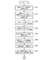
次に、図3から図5を参照し、本発明の実施形態に係る液滴吐出装置の動作(液滴吐出方法)について説明する。
図3及び図4は基板5に回路パターンを形成する場合のフローチャート図、図5は本実施形態で形成される回路パターンを示す斜視図であって、図5(a)から図5(c)は回路パターンが形成される過程を示す図である。
【0033】
図5(c)に示すように、回路パターン(パターン)Pは、導電性配線(機能層)P1、P3と、絶縁膜(機能層)P2とから構成されている。ここで、導電性配線P1、P3を形成するために、金属微粒子等を含む材料液体を使用し、また、絶縁膜P2を形成するために、有機絶縁材料等を含む材料液体を使用する。更に、上記の各材料液体を吐出する吐出ヘッド3aが吐出ヘッド群3に配置されている。
【0034】
次に、図3及び図4のフローチャート図に基づいて、基板5上に回路パターンPを形成する液滴吐出方法について説明する。
まず、液滴吐出対象となる基板のサイズ、液滴吐出分解能を決定する(ステップ100)。
次に、CADデータ操作部24により、回路パターンPのCADデータをビットマップデータ作成部26に出力する(ステップ101)。
【0035】
ここで、ステップ101について詳述する。
まず、レイヤ作成部24aによって回路パターンPを構成する各層(P1、P3、P2)をCADデータのレイヤとして作成すると共に、レイヤ厚設定部24bによって当該レイヤの膜厚を設定する。ここで、レイヤの膜厚を設定することにより、自動的に吐出ヘッド3aから吐出される液滴の吐出回数と液滴の吐出量とが設定される。
【0036】
次に、ビットマップデータ作成部26は、CADデータの各レイヤに基づいてそれぞれのビットマップデータを作成し、液滴吐出データ作成部30に出力する(ステップ102)。
【0037】
次に、ビットマップデータ処理部28は、液滴吐出の仕方に応じて上記のビットマップデータを処理する(ステップ103)。即ち、吐出ヘッド群3のノズルピッチと画素ピッチが合わない場合、要求される液滴量が1度に打てない場合、あるいは1度に打つと液滴が固まってしまい目的とするパターンが得られない場合等を考慮してビットマップデータを変更する処理を行う。
【0038】
次に、使用する吐出ヘッド群3のヘッド個数、配置を決定し、吐出ヘッド設定値入力部22により液滴吐出データ作成部に入力する(ステップ104)。
次に、液滴吐出データ作成部30では、ビットマップデータ処理部28及び吐出ヘッド設定値入力部22より入力されたデータに基づいて、回路パターンPの各層(P1、P2、P3)毎に液滴吐出データを作成する(ステップ105)。
次に、ステージ4の搬送機構と、ヘッド駆動制御部40とによって基板5を搬送し、位置決めを行う(ステップ106)。
【0039】
次に、全ての液滴吐出データを液滴吐出データ転送部32に転送する(ステップ107)。
液滴吐出データ転送部32では、まず、導電性配線P1を形成するにあたり、最初のパスの液滴吐出データをスイッチ群34を介して吐出ヘッド群3に転送する(ステップ108)。次に、吐出ヘッド群3のノズルに対向する位置まで搬送された基板5に対して吐出ヘッド群3より液滴が吐出される(ステップ109)。
【0040】
次に、最初のパスについて液滴吐出が終了したか否かが判定される(ステップ110)。ステップ110の判定が否定された場合にはステップ109に戻り、既述した処理を繰り返す。また、ステップ110の判定が肯定された場合には、次のパスの液滴吐出データを、スイッチ群34を介して吐出ヘッド群3に転送する(ステップ111)。次に、既述したように基板5に対して吐出ヘッド群3より液滴が吐出される(ステップ112)。
【0041】
次に、全てのパスについて液滴吐出が終了したか否かが判定される(ステップ113)。ステップ113の判定が否定された場合にはステップ111に戻り、既述した処理を繰り返す。また、ステップ113の判定が肯定されると、図5(a)に示すように導電性配線P1が形成されたことになる。続いて、回路パターンPの全ての層(P1、P2、P3)を形成したが否か判定される(ステップ114)。ステップ114の判定が否定された場合、即ち、絶縁膜P2と導電性配線P3とが形成されていない場合に、ステップ108に戻り、既述した処理を繰り返すことによって、図5(b)、(c)に示すように絶縁膜P2と導電性配線P3とが形成される。
そして、ステップ114の判定が肯定された場合、即ち、回路パターンPの全ての層(P1、P2、P3)が形成され場合に、基板5がステージ4の搬送機構により他の工程に移送するように搬出される(ステップ115)。
【0042】
上述したように、回路パターンPを液滴の吐出で形成するにあたり、当該回路パターンをCADデータとして作成することができる。また、このように作成されたCADデータを変換することによりビットマップデータを作成することができる。また、当該ビットマップデータに基づいて液滴吐出データを作成した後に、当該液滴吐出データに基づいて吐出ヘッドから基板上の所定の位置に吐出することにより、基板5上に回路パターンPを形成することが可能となる。
【0043】
また、CADデータを構成するレイヤに基づいて複数のビットマップデータを作成することができる。また、当該複数のビットマップデータに基づいて複数の液滴吐出データを作成することができる。更に、当該複数の液滴吐出データに基づいて液滴を吐出することによって、複数の層(P1、P2、P3)を形成することができる。
【0044】
また、吐出ヘッド群3が異なる種類の材料液体毎に吐出ヘッド3aを使用し、当該複数の材料液体を吐出し分けることによって、複数の層(P1、P2、P3)からなる回路パターンPを形成することができる。
【0045】
また、レイヤの膜厚に基づいて、更に吐出される液滴に含まれる材料含有量等を加味し、液滴の吐出回数と、液滴の吐出量とを設定することが可能となる。
【0046】
次に、本発明の液滴吐出装置の他の実施形態について説明する。
図6は液滴吐出装置の構成を示す構成図である。
本実施形態においては、既に説明した構成及び動作についての説明を省略し、異なる部分のみについて説明する。
【0047】
図6に示すように液滴吐出装置81は、第1の液滴吐出部(液滴吐出ユニット)U1と、第2の液滴吐出部(液滴吐出ユニット)U2と、第3の液滴吐出部(液滴吐出ユニット)U3と、基板搬送部U4と、基板搬入部U5と、基板搬出部U6とを備えた構成となっている。
第1の液滴吐出部U1と、第2の液滴吐出部U2と、第3の液滴吐出部U3のそれぞれは、1種類の材料液体を液滴として吐出するための吐出ヘッド3aと、当該吐出ヘッド3aと基板5とを相対移動させるためのステージ4と、これらの動作を制御する制御装置2とを備えた構成となっている。また、第1及び第3の液滴吐出部U1、U3のそれぞれは、導電性配線P1、P3を形成するための金属微粒子を含む材料異なる材料液体の液滴を吐出するものである。また、第2の液滴吐出部U2は、絶縁膜P2を形成するための有機絶縁材料等を含む材料液体の液滴を吐出するものである。従って、各液滴吐出部U1、U2、U3が液滴を吐出することにより、導電性配線P1、P3と絶縁膜P2とを形成し、最終的に基板5上に回路パターンPを形成するようになっている。
【0048】
また、基板搬送部U4は、基板搬入部U5から搬入された基板5を各液滴吐出部U1、U2、U3に搬送し、最終的に回路パターンPが形成された基板5を基板搬出部6から搬出するものである。
【0049】
このように構成された液滴吐出装置81による液滴吐出方法について説明する。
まず、基板搬送部U4は基板搬送部U5から第1の液滴吐出部U1に基板5を搬送する。当該第1の液滴吐出部U1においては、先に記載の液滴吐出方法によって、金属微粒子を含む材料液体を吐出することで、図5(a)に示す導電性配線P1を形成する。
次に、基板搬送部U4は第1の液滴吐出部U1から第2の液滴吐出部U2に基板5を搬送する。当該第2の液滴吐出部U2においては、先に記載の液滴吐出方法によって、有機絶縁材料を含む材料液体を吐出することで、図5(b)に示す絶縁膜P2を形成する。
次に、基板搬送部U4は第2の液滴吐出部U2から第3の液滴吐出部U3に基板5を搬送する。当該第3の液滴吐出部U3においては、先に記載の液滴吐出方法によって、金属微粒子を含む材料液体を吐出することで、図5(c)に示す絶縁膜P3を形成する。
次に、基板搬送部U4は第3の液滴吐出部U3から基板搬出部U6に基板5を搬送する。
【0050】
上述したように、各液滴吐出部U1、U2、U3を用いて液滴を吐出し分けることにより、複数の層(P1、P2、P3)からなる回路パターンPを形成することができる。
【0051】
次に、本発明の液滴吐出方法を用いて、液晶表示装置を製造する過程について詳述する。
図7は、液晶表示装置を説明するための図であって、図7(a)は液晶表示装置の画像表示領域を構成する、スイッチング素子等の各種素子及び配線等の等価回路であり、図7(b)は液晶表示装置の要部を示し、各画素が備えるスイッチング素子と画素電極との構造を説明するための斜視図である。
なお、既に説明した構成及び動作についての説明を省略し、異なる部分のみについて説明する。
【0052】
まず、本発明の液滴吐出方法によって形成される液晶表示装置について説明する。
図7(a)に示すように液晶表示装置200は、マトリクス状に配置された走査線(機能層)201及びデータ線(機能層)202と、画素電極(機能層)230と、当該画素電極230を制御するための画素スイッチング用TFT(機能層)210とが複数形成された回路パターンを有している。走査線201においては、パルス的に走査信号Q1、Q2、…、Qmが供給されるようになっており、データ線202においては、画像信号R1、R2、…、Rnが供給されるようになっている。更に、走査線201及びデータ線202は後述するようにTFT210と接続されており、走査信号Q1、Q2、…、Qm及び画像信号R1、R2、…、Rnによって、TFT210が駆動するようになっている。更に、所定レベルの画像信号R1、R2、…、Rnを一定期間保持する蓄積容量(機能層)220が形成され、当該蓄積容量220には容量線(機能層)203が接続されている。
【0053】
更に、図7(b)に示すようにTFT210は、所謂ボトムゲート型(逆スタガ型)構造のTFTであって、その具体的な構造としては、液晶表示装置200の基材となる絶縁基板200aと、絶縁基板200aの表面に形成された下地保護膜(機能層)200Iと、ゲート電極(機能層)210Gと、ゲート絶縁膜(機能層)210Iと、チャネル領域(機能層)210Cと、チャネル保護用の絶縁膜(機能層)211Iとがこの順序で積層されたものである。絶縁膜(機能層)211Iの両側にはソース領域(機能層)210S及びドレイン領域(機能層)210Dが形成され、これらのソース・ドレイン領域210S、210Dの表面にはソース電極(機能層)211S及びドレイン電極(機能層)211Dが形成されている。
【0054】
更に、それらの表面側には層間絶縁膜212Iと、ITO等の透明電極からなる画素電極(機能層)230とが形成され、画素電極230はコンタクトホールを介してドレイン電極211Dに電気的に接続されている。
ここで、ゲート電極210Gは走査線201の一部分であり、また、ソース電極211Sはデータ線202の一部分である。
【0055】
次に、このように構成された液晶表示装置200の回路パターンの製造方法について簡単に説明する。
当該回路パターンは、上記各機能層に対応した複数のレイヤをCADデータとして作成し、当該CADデータからビットマップデータを作成し、更に、液滴吐出データを作成する。更に、液滴吐出データに基づいて吐出ヘッド3a(吐出ヘッド群3)が液滴を吐出する。当該液滴の材料液体は、各機能層に応じた材料が採用される。
【0056】
上述したように、本発明の液滴吐出方法を用いることにより、積層構造のパターンを形成することが可能となる。
【図面の簡単な説明】
【図1】本発明の液滴吐出装置の構成を示す斜視図。
【図2】本発明の液滴吐出装置の制御装置の機能を説明するブロック図。
【図3】本発明の液滴吐出装置で画素を形成するフローチャート図。
【図4】図3に続くフローチャート図。
【図5】本発明の液滴吐出方法で形成される回路パターンを示す斜視図。
【図6】本発明の液滴吐出装置の構成を示す構成図。
【図7】本発明の液滴吐出方法で形成される液晶表示装置を示す図。
【符号の説明】
1…液滴吐出装置、3…吐出ヘッド群、3a…吐出ヘッド、5…基板、P…回路パターン(パターン)、P1、P3…導電性配線(機能層)、P2…絶縁膜(機能層)、U1…第1の液滴吐出部(液滴吐出ユニット)、U2…第2の液滴吐出部(液滴吐出ユニット)、U3…第3の液滴吐出部(液滴吐出ユニット)、24…CADデータ操作部(CADデータ作成手段)、26…ビットマップデータ作成部(ビットマップデータ作成手段)、30…液滴吐出データ作成部(作成手段)、24b…レイヤ厚設定部(設定手段)[0001]
TECHNICAL FIELD OF THE INVENTION
The present invention relates to a droplet discharging method and a droplet discharging device.
[0002]
[Prior art]
2. Description of the Related Art In recent years, liquid crystal devices, electroluminescent devices, and the like have been used as display units of electronic devices such as mobile phones and portable computers. For example, in a liquid crystal device, filter elements of red, green, and blue dot shapes are arranged in a predetermined arrangement such as a so-called stripe arrangement, delta arrangement, or mosaic arrangement on a surface of a substrate formed of glass, plastic, or the like. A color filter is formed.
[0003]
In addition, as a method of forming such a color filter, droplets are ejected onto an acrylic resin applied on a glass substrate while scanning a dye droplet ejection head for ejecting droplets of red, green, and blue pigments. Then, a method of fixing is known (for example, see Patent Document 1).
[0004]
[Patent Document 1]
JP-A-2-173703 (
[0005]
[Problems to be solved by the invention]
By the way, since each droplet needs to be fixed at a predetermined position on the substrate, when forming a large number of color filters on a large-area substrate, a mechanism for precisely adjusting the position of the substrate is required. Met. In particular, when a pattern formed on a substrate is a fine color filter, a circuit having a complicated shape, or the like, a high-precision alignment mechanism must be provided. Furthermore, when it takes time to drive the mechanism for adjusting the position of the substrate, the tact time per substrate may be long.
[0006]
The present invention has been made in view of such a problem, and an object of the present invention is to provide a droplet discharge method and a droplet discharge device capable of forming a highly accurate pattern on a substrate with a simple configuration. .
[0007]
[Means for Solving the Problems]
In order to achieve the above object, the present invention employs the following solutions.
That is, in the droplet discharge method of the present invention, a droplet is formed such that a discharge head discharges a droplet to a substrate and forms a pattern on the substrate while relatively moving a discharge head having a droplet discharge means and the substrate. In the ejection method, CAD (computer aided design) data defined by a combination of a plurality of vector data is created according to the shape of a pattern, and the ejection position of a droplet is defined by an XY grid based on the CAD data. By creating droplet-discharged data for discharging droplets based on the bitmap data, and driving the droplet-discharge means in accordance with the droplet-discharge data. Is formed.
[0008]
Here, the “droplet discharging means” has a function of changing the volume in the discharge head according to a predetermined voltage waveform supplied to the piezoelectric element or the like, and discharging the pressed liquid droplets accordingly. Have The droplet discharging means is not limited to an electromechanical transducer using a piezoelectric element or the like. For example, an electrothermal transducer as an energy generating element, or a continuous type such as a charge control type and a pressure vibration type may be used. , An electrostatic suction method or the like.
The “droplet ejection data” is data for supplying the above-described voltage waveform to the droplet ejection unit, that is, data for controlling the ejection of droplets by the droplet ejection unit. The droplet discharge data includes data for relatively moving the discharge head and the substrate, that is, data for determining the droplet discharge position on the substrate. The data format of the droplet ejection data is time-series data including “0” and “1”, and is stored in a ROM (Read Only Memory) or a RAM (Random Access Memory).
The “pattern” is a pattern formed by discharging a material that can be discharged as droplets onto a substrate at a predetermined position, for example, R (red), G (green), B (blue) A pixel pattern of an RGB color filter composed of, for example, a coil or an antenna having a labyrinth structure, a capacitance composed of a capacitive element such as a capacitor, a circuit pattern having a resistance, a TFT (Thin Film Transistor) having a semiconductor, or the like. Switching element, a pattern having a pixel electrode or the like connected to the switching element, or a liquid crystal material or an alignment film material that needs to be locally discharged. Here, the switching element means an element formed of a material that can be discharged as a liquid material.
The “substrate” is a droplet discharge target on which a pattern is formed by discharging the above-described droplet. As the material, various kinds of materials are adopted. For example, a substrate such as glass is used when the material has transparency, and a metal substrate is used when transparency is not required. Although the size of the substrate is not limited, the present invention particularly means a large substrate having a size exceeding 1 m.
According to the present invention, by using a computer having a display unit such as a display and an input unit such as a keyboard, a pattern formed by discharging the droplets can be created in advance as CAD data.
Also, by converting the CAD data created in this way, bitmap data can be created.
Further, after creating droplet ejection data based on the bitmap data, it is possible to form a pattern on the substrate by ejecting the ejection head to a predetermined position on the substrate based on the droplet ejection data. It becomes possible.
[0009]
Further, the present invention is the droplet discharging method described above, wherein the pattern is formed by laminating a plurality of functional layers having a predetermined function, and the CAD data is a plurality of layer data corresponding to the functional layer. Has a plurality of bitmap data based on the plurality of layer data, creates a plurality of droplet ejection data based on the plurality of bitmap data, and according to the plurality of droplet ejection data. By driving the droplet discharge means, a pattern comprising a plurality of functional layers is formed.
Here, the “functional layer” means each layer constituting the above-mentioned pattern, and means, for example, each layer of the above-mentioned inductance, capacitance, resistance, switching element and the like. That is, the above-mentioned pattern is formed by laminating such functional layers.
Further, “layer data” means a so-called layer, which is created in advance by a computer or the like in order to form the functional layer.
According to the present invention, a plurality of bitmap data can be created based on such a plurality of layer data. Also, a plurality of droplet ejection data can be created based on the plurality of bitmap data. Further, a plurality of functional layers can be formed by discharging droplets based on the plurality of droplet discharge data. Therefore, a pattern in which a plurality of functional layers are stacked can be formed.
[0010]
Further, the present invention is the droplet discharge method described above, comprising a discharge head group consisting of a plurality of discharge heads, the discharge heads of the discharge head group for each of a plurality of functional layers to separately discharge droplets, It is characterized by forming a pattern.
Here, the discharge head group includes, for example, a first discharge head that discharges a droplet containing a metal material, a second discharge head that discharges a droplet containing an insulating film material, and a transparent electrode material. And a third ejection head for ejecting the droplets. First, when a functional layer made of metal wiring is formed on a substrate, bitmap data is created from layer data for forming metal wiring, and then droplet ejection data is created. The first ejection head ejects a droplet containing a metal material based on the above. Thereafter, when forming a functional layer of the insulating film and the transparent electrode, respective droplet ejection data are created from the layer data for forming the insulating film and the transparent electrode in the same manner as described above, and the second Discharge heads discharge droplets containing an insulating film material, and the third discharge head discharges droplets containing a transparent electrode material.
As described above, the ejection head group includes the first, second, and third ejection heads, and droplets are ejected using these ejection heads to form a pattern including a plurality of functional layers. be able to.
[0011]
Further, the present invention is the above-described droplet discharging method, comprising a plurality of droplet discharging units in which a discharging head discharges droplets onto a substrate to form a functional layer on the substrate, and a plurality of droplets. Each of the discharge units discharges droplets for each of the plurality of functional layers on the substrate to form a pattern including a plurality of functional layers.
Here, for example, a first droplet discharging unit that discharges a droplet containing a metal material, a second droplet discharging unit that discharges a droplet containing an insulating film material, and a transparent electrode material are contained. A case in which a pattern is formed using a third droplet discharge unit that discharges droplets will be described. First, when a functional layer made of metal wiring is formed on a substrate, bitmap data is created from layer data for forming metal wiring, and then droplet ejection data is created. The droplet containing the metal material is discharged onto the substrate by the first droplet discharge unit based on the above. Thereafter, when forming a functional layer of the insulating film and the transparent electrode, respective droplet ejection data are created from the layer data for forming the insulating film and the transparent electrode in the same manner as described above, and the second Droplets containing the insulating film material are ejected by the droplet ejection unit, and droplets containing the transparent electrode material are ejected by the third droplet ejection unit. It is preferable that a transport unit for transporting the substrate is provided between the first, second, and third droplet discharge units.
In this manner, a pattern including a plurality of functional layers can be formed by separately discharging droplets using the first, second, and third droplet discharge units.
[0012]
Further, the present invention is the above-described droplet discharging method, wherein the layer data includes film thickness data for defining the film thickness of the functional layer, and the liquid discharged from the discharge head is based on the film thickness data. It is characterized in that the number of times of droplet ejection and the amount of droplet ejection are set.
Here, “film thickness data” means the film thickness of the material constituting the functional layer. For example, when forming a metal wiring or the like, a method of discharging a liquid in which metal fine particles are dispersed in a volatile solvent as droplets is employed. In this method, the number of discharges and the discharge amount of the droplets are set in consideration of the content of the metal fine particles, and the deterioration or volume change of the material due to the drying process and the heat treatment for precipitating the metal fine particles. .
ADVANTAGE OF THE INVENTION According to this invention, it is possible to set the frequency | count of a droplet discharge, and the discharge amount of a droplet further considering the material content etc. contained in the droplet discharged based on film thickness data. It becomes.
[0013]
In addition, the droplet discharge apparatus of the present invention discharges droplets onto a substrate while relatively moving a discharge head having droplet discharge means and a substrate, thereby forming a pattern on the substrate. An ejection apparatus, a CAD data creating means for creating CAD data defined by a combination of a plurality of vector data in accordance with a shape of a pattern, and a discharge position of a droplet defined by an XY grid based on the CAD data. Bitmap data creating means for creating the obtained bitmap data, and creating means for creating droplet ejection data for ejecting droplets based on the bitmap data. The pattern is formed by driving the droplet discharge means in accordance with (1).
According to the present invention, the pattern formed by the ejection of the droplets can be created in advance as CAD data by the CAD data creation means.
Also, bitmap data can be created by the bitmap data creation means.
Further, the droplet ejection data can be created by the creating means based on the bitmap data.
Further, a pattern can be formed on the substrate by discharging the liquid from the discharge head to a predetermined position on the substrate based on the droplet discharge data.
[0014]
Further, the present invention is the above-described droplet discharging apparatus, wherein the pattern is formed by laminating a plurality of functional layers having a predetermined function, and the CAD data creating means corresponds to the plurality of functional layers. A plurality of layer data is created, the bitmap data creating unit creates a plurality of bitmap data based on the plurality of layer data, and the creating unit creates a plurality of droplet ejection data based on the plurality of bitmap data. The method is characterized in that a pattern formed of a plurality of functional layers is formed by driving the droplet discharge means in accordance with the plurality of droplet discharge data.
According to the present invention, the CAD data creation means can create a plurality of layer data. Further, the bitmap data creation means can create a plurality of bitmap data based on the plurality of layer data. Further, the creating means can create a plurality of droplet ejection data based on the plurality of bitmap data. Further, a plurality of functional layers can be formed by discharging droplets based on a plurality of droplet discharge data. Therefore, a pattern in which a plurality of functional layers are stacked can be formed.
[0015]
According to another aspect of the present invention, there is provided the droplet discharge device described above, further comprising a discharge head group including a plurality of the discharge heads, wherein the discharge head group discharges droplets for each of a plurality of functional layers. And
Here, the discharge head group includes, for example, a first discharge head that discharges a droplet containing a metal material, a second discharge head that discharges a droplet containing an insulating film material, and a transparent electrode material. And a third ejection head for ejecting the droplets. First, when a functional layer made of metal wiring is formed on a substrate, bitmap data is created from layer data for forming metal wiring, and then droplet ejection data is created. The first ejection head ejects a droplet containing a metal material based on the above. Thereafter, when forming a functional layer of the insulating film and the transparent electrode, respective droplet ejection data are created from the layer data for forming the insulating film and the transparent electrode in the same manner as described above, and the second Discharge heads discharge droplets containing an insulating film material, and the third discharge head discharges droplets containing a transparent electrode material.
As described above, the ejection head group includes the first, second, and third ejection heads, and droplets are ejected using these ejection heads to form a pattern including a plurality of functional layers. be able to.
[0016]
Further, the present invention is the droplet discharge device according to the above, comprising a plurality of droplet discharge units each having a discharge head, wherein each of the plurality of droplet discharge units is provided for each of a plurality of functional layers. Are discharged separately.
Here, for example, a first droplet discharging unit that discharges a droplet containing a metal material, a second droplet discharging unit that discharges a droplet containing an insulating film material, and a transparent electrode material are contained. A case in which a pattern is formed using a third droplet discharge unit that discharges droplets will be described. First, when a functional layer made of metal wiring is formed on a substrate, bitmap data is created from layer data for forming metal wiring, and then droplet ejection data is created. The droplet containing the metal material is discharged onto the substrate by the first droplet discharge unit based on the above. Thereafter, when forming a functional layer of the insulating film and the transparent electrode, respective droplet ejection data are created from the layer data for forming the insulating film and the transparent electrode in the same manner as described above, and the second Droplets containing the insulating film material are ejected by the droplet ejection unit, and droplets containing the transparent electrode material are ejected by the third droplet ejection unit. It is preferable that a transport unit for transporting the substrate is provided between the first, second, and third droplet discharge units.
In this manner, a pattern including a plurality of functional layers can be formed by separately discharging droplets using the first, second, and third droplet discharge units.
[0017]
Further, the present invention is the droplet discharge device according to the above, wherein the layer data includes film thickness data that defines the film thickness of the functional layer, and the CAD data creation means includes: Setting means for setting the number of ejections of the droplets ejected from the ejection head and the ejection amount of the droplets based on the ejection head.
Here, the “setting means” refers to the ratio of the material of the functional layer contained in the droplets, and the number of ejections and the number of ejections of the droplets, taking into account the alteration and volume change of the material due to processing such as drying. The quantity is what you set. For example, in the case of forming a metal wiring or the like, a method of discharging a liquid in which metal fine particles are dispersed in a volatile solvent as droplets is used. In this method, the number of discharges and the discharge amount of the droplets are set in consideration of the content of the metal fine particles, the deterioration and the volume change of the material due to the drying treatment and the heat treatment for precipitating the metal fine particles, and the like. .
ADVANTAGE OF THE INVENTION According to this invention, it is possible to set the frequency | count of a droplet discharge, and the discharge amount of a droplet further considering the material content etc. contained in the droplet discharged based on film thickness data. It becomes.
[0018]
BEST MODE FOR CARRYING OUT THE INVENTION
Hereinafter, the present invention will be described in detail.
FIG. 1 is a perspective view illustrating a configuration of a droplet discharge device according to an embodiment of the present invention.
[0019]
As shown in FIG. 1, the droplet discharge device 1 includes a
In such a droplet discharge device 1, the
Next, each component will be described.
In the following description, the arrangement direction of the
[0020]
The
[0021]
The
The droplet discharging means of the
[0022]
Further, a liquid tank for storing the material liquid is connected to each of the plurality of ejection heads 3a via a flow path such as a pipe. Here, by storing different types of material liquids in the respective liquid material tanks, different material liquids can be formed on the substrate from each of the ejection heads 3a. That is, the
[0023]
In addition, the above-described
Further, the
[0024]
The stage 4 includes a mounting
Furthermore, the stage 4 is configured to be movable along a Y-
[0025]
The substrate 5 is an object on which a pattern is formed in the present embodiment. As a material, a transparent substrate such as glass is used. However, when transparency is not required, a metal plate or the like may be employed. The size of the substrate 5 is more than 1 m in length and width.
Examples of the pattern formed on the substrate 5 include a pixel pattern formed by a color filter having an RGB color and a metal wiring when a TFT circuit is formed.
[0026]
The
[0027]
Next, a detailed configuration of the
FIG. 2 is a block diagram for explaining functions of the
As shown in FIG. 2, the
[0028]
Here, the droplet discharge data setting value input unit 20 determines the dimensions of the substrate 5, the dimensions of the chips for cutting the substrate 5 into a plurality of chips, the pitch of adjacent chips, the arrangement of pixels (patterns), It has a function of setting the number of pixels, the dimensions of the pixels (vertical and horizontal sizes of the pixels), and the pitch of adjacent pixels.
The ejection head setting
[0029]
The CAD
Here, when the pattern is a laminated structure formed by laminating a plurality of layers (functional layers), the
[0030]
Further, the bitmap
Further, the droplet discharge
[0031]
The droplet discharge data transfer
The
The
Further, the head
Further, the head
Further, the droplet discharge
[0032]
Next, an operation (a droplet discharge method) of the droplet discharge device according to the embodiment of the present invention will be described with reference to FIGS.
3 and 4 are flow charts in the case of forming a circuit pattern on the substrate 5, and FIG. 5 is a perspective view showing a circuit pattern formed in the present embodiment, which is shown in FIGS. 5 (a) to 5 (c). FIG. 4 is a diagram showing a process of forming a circuit pattern.
[0033]
As shown in FIG. 5C, the circuit pattern (pattern) P includes conductive wirings (functional layers) P1 and P3 and an insulating film (functional layer) P2. Here, a material liquid containing metal fine particles or the like is used to form the conductive wirings P1 and P3, and a material liquid containing an organic insulating material or the like is used to form the insulating film P2. Further, an
[0034]
Next, a droplet discharging method for forming a circuit pattern P on the substrate 5 will be described with reference to the flowcharts of FIGS.
First, the size of the substrate to be subjected to droplet ejection and the droplet ejection resolution are determined (step 100).
Next, the CAD
[0035]
Here,
First, each layer (P1, P3, P2) constituting the circuit pattern P is created as a layer of CAD data by the
[0036]
Next, the bitmap
[0037]
Next, the bitmap
[0038]
Next, the number and arrangement of the
Next, the droplet discharge
Next, the substrate 5 is transported and positioned by the transport mechanism of the stage 4 and the head drive controller 40 (Step 106).
[0039]
Next, all the droplet discharge data is transferred to the droplet discharge data transfer unit 32 (Step 107).
In forming the conductive wiring P1, the droplet discharge data transfer
[0040]
Next, it is determined whether the droplet discharge has been completed for the first pass (step 110). If the determination in
[0041]
Next, it is determined whether the droplet discharge has been completed for all the passes (step 113). If the determination at
Then, when the determination in
[0042]
As described above, when forming the circuit pattern P by discharging droplets, the circuit pattern can be created as CAD data. Also, by converting the CAD data created in this way, bitmap data can be created. Further, after the droplet ejection data is created based on the bitmap data, the circuit pattern P is formed on the substrate 5 by ejecting the ejection head to a predetermined position on the substrate based on the droplet ejection data. It is possible to do.
[0043]
Also, a plurality of bitmap data can be created based on the layers constituting the CAD data. Also, a plurality of droplet ejection data can be created based on the plurality of bitmap data. Further, a plurality of layers (P1, P2, P3) can be formed by discharging droplets based on the plurality of droplet discharge data.
[0044]
Further, the
[0045]
In addition, it is possible to set the number of times of droplet ejection and the amount of droplet ejection by further taking into account the material content and the like contained in the droplets to be ejected based on the film thickness of the layer.
[0046]
Next, another embodiment of the droplet discharge device of the present invention will be described.
FIG. 6 is a configuration diagram showing the configuration of the droplet discharge device.
In the present embodiment, the description of the configuration and operation already described is omitted, and only different portions will be described.
[0047]
As shown in FIG. 6, the
Each of the first droplet discharging unit U1, the second droplet discharging unit U2, and the third droplet discharging unit U3 includes a discharging
[0048]
The substrate transport unit U4 transports the substrate 5 loaded from the substrate loading unit U5 to each of the droplet discharge units U1, U2, and U3, and finally transfers the substrate 5 on which the circuit pattern P is formed to the substrate transport unit 6 It is carried out from.
[0049]
A droplet discharging method by the
First, the substrate transport unit U4 transports the substrate 5 from the substrate transport unit U5 to the first droplet discharging unit U1. In the first droplet discharge unit U1, the conductive liquid P1 shown in FIG. 5A is formed by discharging a material liquid containing metal fine particles by the droplet discharge method described above.
Next, the substrate transport unit U4 transports the substrate 5 from the first droplet discharging unit U1 to the second droplet discharging unit U2. In the second droplet discharge unit U2, the insulating film P2 shown in FIG. 5B is formed by discharging the material liquid containing the organic insulating material by the droplet discharge method described above.
Next, the substrate transport unit U4 transports the substrate 5 from the second droplet discharging unit U2 to the third droplet discharging unit U3. In the third droplet discharging section U3, the insulating film P3 shown in FIG. 5C is formed by discharging the material liquid containing the fine metal particles by the droplet discharging method described above.
Next, the substrate transport unit U4 transports the substrate 5 from the third droplet discharge unit U3 to the substrate unloading unit U6.
[0050]
As described above, the circuit pattern P including a plurality of layers (P1, P2, P3) can be formed by separately discharging the droplets using the respective droplet discharge units U1, U2, and U3.
[0051]
Next, a process of manufacturing a liquid crystal display device using the droplet discharging method of the present invention will be described in detail.
FIG. 7 is a diagram for explaining the liquid crystal display device, and FIG. 7A is an equivalent circuit such as various elements such as switching elements and wirings that constitute an image display area of the liquid crystal display device. FIG. 7B is a perspective view illustrating a main part of the liquid crystal display device and illustrating a structure of a switching element and a pixel electrode included in each pixel.
The description of the configuration and operation already described is omitted, and only different portions will be described.
[0052]
First, a liquid crystal display device formed by the droplet discharging method of the present invention will be described.
As shown in FIG. 7A, the liquid
[0053]
Further, as shown in FIG. 7B, the
[0054]
Further, an interlayer insulating film 212I and a pixel electrode (functional layer) 230 made of a transparent electrode such as ITO are formed on the surface side thereof, and the
Here, the gate electrode 210G is a part of the
[0055]
Next, a brief description will be given of a method of manufacturing a circuit pattern of the liquid
The circuit pattern creates a plurality of layers corresponding to the respective functional layers as CAD data, creates bitmap data from the CAD data, and creates droplet ejection data. Further, the
[0056]
As described above, by using the droplet discharging method of the present invention, a pattern having a laminated structure can be formed.
[Brief description of the drawings]
FIG. 1 is a perspective view showing a configuration of a droplet discharge device of the present invention.
FIG. 2 is a block diagram illustrating functions of a control device of the droplet discharge device of the present invention.
FIG. 3 is a flowchart of forming a pixel by the droplet discharge device of the present invention.
FIG. 4 is a flowchart following FIG. 3;
FIG. 5 is a perspective view showing a circuit pattern formed by the droplet discharging method of the present invention.
FIG. 6 is a configuration diagram showing a configuration of a droplet discharge device of the present invention.
FIG. 7 is a diagram showing a liquid crystal display device formed by the droplet discharging method of the present invention.
[Explanation of symbols]
DESCRIPTION OF SYMBOLS 1 ... Droplet discharge device, 3 ... Discharge head group, 3a ... Discharge head, 5 ... Substrate, P ... Circuit pattern (pattern), P1, P3 ... Conductive wiring (functional layer), P2 ... Insulating film (functional layer) U1, a first droplet discharge unit (droplet discharge unit), U2, a second droplet discharge unit (droplet discharge unit), U3, a third droplet discharge unit (droplet discharge unit), 24 ... CAD data operation unit (CAD data creation unit), 26 ... bitmap data creation unit (bitmap data creation unit), 30 ... droplet ejection data creation unit (creation unit), 24b ... layer thickness setting unit (setting unit)
Claims (10)
前記パターンの形状に応じて、複数のベクトルデータの組み合わせによって規定されたCAD(computer aided design)データを作成し、
当該CADデータに基づいて前記液滴の吐出位置がXY格子によって規定されたビットマップデータを作成し、
当該ビットマップデータに基づいて前記液滴の吐出を行うための液滴吐出データを作成し、
当該液滴吐出データに応じて前記液滴吐出手段を駆動させることにより前記パターンを形成することを特徴とする液滴吐出方法。A droplet discharge method in which the discharge head discharges droplets onto the substrate while relatively moving a discharge head including a droplet discharge unit and the substrate, and forms a pattern on the substrate,
Creating CAD (computer aided design) data defined by a combination of a plurality of vector data according to the shape of the pattern;
Creating bitmap data in which the discharge position of the droplet is defined by an XY grid based on the CAD data;
Create droplet discharge data for discharging the droplet based on the bitmap data,
A droplet discharging method, wherein the pattern is formed by driving the droplet discharging means in accordance with the droplet discharging data.
前記CADデータは、前記機能層に対応した複数の層データを有し、
当該複数の層データに基づいて複数の前記ビットマップデータを作成し、
当該複数のビットマップデータに基づいて複数の前記液滴吐出データを作成し、
当該複数の液滴吐出データに応じて前記液滴吐出手段を駆動させることにより前記複数の機能層からなる前記パターンを形成することを特徴とする請求項1に記載の液滴吐出方法。The pattern is formed by laminating a plurality of functional layers having a predetermined function,
The CAD data has a plurality of layer data corresponding to the functional layer,
Create a plurality of the bitmap data based on the plurality of layer data,
Create a plurality of droplet ejection data based on the plurality of bitmap data,
2. The droplet discharging method according to claim 1, wherein the pattern including the plurality of functional layers is formed by driving the droplet discharging unit in accordance with the plurality of droplet discharging data.
前記複数の機能層毎に前記吐出ヘッド群の前記吐出ヘッドが前記液滴を吐出し分けることにより、前記パターンを形成することを特徴とする請求項1又は請求項2に記載の液滴吐出方法。A discharge head group including a plurality of the discharge heads,
3. The droplet discharge method according to claim 1, wherein the discharge head of the discharge head group discharges the droplets separately for each of the plurality of functional layers to form the pattern. 4. .
前記複数の液滴吐出ユニットのそれぞれが、前記基板上に前記複数の機能層毎に前記液滴を吐出し分けることにより、前記複数の機能層からなる前記パターンを形成することを特徴とする請求項1又は請求項2に記載の液滴吐出方法。The discharge head discharges the liquid droplets to the substrate to form the functional layer on the substrate, comprising a plurality of droplet discharge units,
Each of the plurality of droplet discharge units discharges the droplet for each of the plurality of functional layers on the substrate, thereby forming the pattern including the plurality of functional layers. 3. The droplet discharging method according to claim 1 or 2.
当該膜厚データに基づいて、前記吐出ヘッドから吐出される前記液滴の吐出回数と、当該液滴の吐出量と、を設定することを特徴とする請求項1から請求項4のいずれかに記載の液滴吐出方法。The layer data includes film thickness data that defines the film thickness of the functional layer,
The discharge number of the liquid droplets discharged from the discharge head and the discharge amount of the liquid droplets are set based on the film thickness data. The droplet discharging method described in the above.
前記パターンの形状に応じて、複数のベクトルデータの組み合わせによって規定されたCADデータを作成するCADデータ作成手段と、
当該CADデータに基づいて前記液滴の吐出位置がXY格子によって規定されたビットマップデータを作成するビットマップデータ作成手段と、
当該ビットマップデータに基づいて前記液滴の吐出を行うための液滴吐出データを作成する作成手段と、
を具備し、
当該液滴吐出データに応じて前記液滴吐出手段を駆動させることにより前記パターンを形成することを特徴とする液滴吐出装置。A droplet discharge device that discharges droplets onto the substrate while relatively moving a discharge head including a droplet discharge unit and a substrate, and forms a pattern on the substrate,
CAD data creation means for creating CAD data defined by a combination of a plurality of vector data according to the shape of the pattern;
Bitmap data creating means for creating bitmap data in which the droplet discharge position is defined by an XY grid based on the CAD data;
Creating means for creating droplet ejection data for ejecting the droplet based on the bitmap data,
With
A droplet discharge apparatus, wherein the pattern is formed by driving the droplet discharge means in accordance with the droplet discharge data.
前記CADデータ作成手段は、前記複数の機能層に対応した複数の層データを作成し、
前記ビットマップデータ作成手段は、前記複数の層データに基づいて複数の前記ビットマップデータを作成し、
前記作成手段は、前記複数のビットマップデータに基づいて複数の前記液滴吐出データを作成し、
当該複数の液滴吐出データに応じて前記液滴吐出手段を駆動させることにより複数の前記機能層からなる前記パターンを形成することを特徴とする請求項6に記載の液滴吐出装置。The pattern is formed by laminating a plurality of functional layers having a predetermined function,
The CAD data creating means creates a plurality of layer data corresponding to the plurality of functional layers,
The bitmap data creating means creates a plurality of the bitmap data based on the plurality of layer data,
The creating means creates a plurality of droplet ejection data based on the plurality of bitmap data,
7. The droplet discharging apparatus according to claim 6, wherein the pattern including the plurality of functional layers is formed by driving the droplet discharging unit in accordance with the plurality of droplet discharging data.
当該吐出ヘッド群は、前記複数の機能層毎に前記液滴を吐出し分けることを特徴とする請求項6又は請求項7に記載の液滴吐出装置。A discharge head group including a plurality of the discharge heads,
The droplet discharge device according to claim 6, wherein the discharge head group discharges the droplet separately for each of the plurality of functional layers.
前記複数の液滴吐出ユニットのそれぞれが、前記複数の機能層毎に前記液滴を吐出し分けることを特徴とする請求項6又は請求項7に記載の液滴吐出装置。Comprising a plurality of droplet discharge units each having the discharge head,
The droplet discharge device according to claim 6, wherein each of the plurality of droplet discharge units discharges the droplet separately for each of the plurality of functional layers.
前記CADデータ作成手段は、前記膜厚データに基づいて、前記吐出ヘッドから吐出される前記液滴の吐出回数と当該液滴の吐出量とを設定する設定手段を具備することを特徴とする請求項6から請求項9のいずれかに記載の液滴吐出装置。The layer data includes film thickness data that defines the film thickness of the functional layer,
The CAD data creation means includes a setting means for setting the number of times of ejection of the droplets ejected from the ejection head and the amount of ejection of the droplets based on the film thickness data. The droplet discharge device according to any one of claims 6 to 9.
Priority Applications (10)
| Application Number | Priority Date | Filing Date | Title |
|---|---|---|---|
| JP2003135791A JP2004337701A (en) | 2003-05-14 | 2003-05-14 | Method and apparatus for discharging liquid drop |
| CNB2004100433042A CN1302928C (en) | 2003-05-14 | 2004-05-12 | Liquid drop blowing-out method and liquid drop blowing-out device |
| CNB2006101000733A CN100445095C (en) | 2003-05-14 | 2004-05-12 | Liquid droplet discharging method, and liquid droplet discharging apparatus |
| KR1020040033486A KR100638154B1 (en) | 2003-05-14 | 2004-05-12 | Liquid droplet discharging method, and liquid droplet discharging apparatus |
| CNB2006101000748A CN100439105C (en) | 2003-05-14 | 2004-05-12 | Liquid droplet discharging method, and liquid droplet discharging apparatus and liquid for manufacturing substrate |
| US10/844,972 US6992746B2 (en) | 2003-05-14 | 2004-05-13 | Liquid droplet discharging method, and liquid droplet discharging apparatus |
| TW093113486A TWI239896B (en) | 2003-05-14 | 2004-05-13 | Liquid droplet discharging method, and liquid droplet discharging apparatus |
| US11/274,767 US7535546B2 (en) | 2003-05-14 | 2005-11-15 | Liquid droplet discharging method, and liquid droplet discharging apparatus |
| KR1020060038010A KR100676159B1 (en) | 2003-05-14 | 2006-04-27 | Liquid droplet discharging method, and liquid droplet discharging apparatus |
| US12/402,932 US20090174859A1 (en) | 2003-05-14 | 2009-03-12 | Liquid droplet discharging method, and liquid droplet discharging apparatus |
Applications Claiming Priority (1)
| Application Number | Priority Date | Filing Date | Title |
|---|---|---|---|
| JP2003135791A JP2004337701A (en) | 2003-05-14 | 2003-05-14 | Method and apparatus for discharging liquid drop |
Related Child Applications (1)
| Application Number | Title | Priority Date | Filing Date |
|---|---|---|---|
| JP2006107474A Division JP4285497B2 (en) | 2006-04-10 | 2006-04-10 | Droplet discharge method, droplet discharge apparatus, and method for manufacturing substrate having switching element |
Publications (1)
| Publication Number | Publication Date |
|---|---|
| JP2004337701A true JP2004337701A (en) | 2004-12-02 |
Family
ID=33525946
Family Applications (1)
| Application Number | Title | Priority Date | Filing Date |
|---|---|---|---|
| JP2003135791A Withdrawn JP2004337701A (en) | 2003-05-14 | 2003-05-14 | Method and apparatus for discharging liquid drop |
Country Status (5)
| Country | Link |
|---|---|
| US (3) | US6992746B2 (en) |
| JP (1) | JP2004337701A (en) |
| KR (2) | KR100638154B1 (en) |
| CN (3) | CN100445095C (en) |
| TW (1) | TWI239896B (en) |
Families Citing this family (19)
| Publication number | Priority date | Publication date | Assignee | Title |
|---|---|---|---|---|
| JP4033174B2 (en) * | 2004-06-10 | 2008-01-16 | セイコーエプソン株式会社 | Liquid crystal substrate manufacturing method and liquid crystal substrate manufacturing apparatus |
| KR20060082641A (en) * | 2005-01-13 | 2006-07-19 | 삼성전자주식회사 | Liquid crystal dropping amount measuring system and method |
| EP2081905B1 (en) * | 2006-07-28 | 2012-09-12 | Boehringer Ingelheim International GmbH | Sulfonyl compounds which modulate the cb2 receptor |
| BRPI0718515A2 (en) * | 2006-09-25 | 2013-11-19 | Boehringer Ingelheim Int | COMPOUNDS THAT MODULATE THE CB2 RECEIVER |
| JP4356740B2 (en) * | 2006-11-29 | 2009-11-04 | セイコーエプソン株式会社 | Wiring pattern forming method, device and electronic apparatus |
| WO2009061652A1 (en) * | 2007-11-07 | 2009-05-14 | Boehringer Ingelheim International Gmbh | Compounds which modulate the cb2 receptor |
| WO2010005782A1 (en) * | 2008-07-10 | 2010-01-14 | Boehringer Ingelheim International Gmbh | Sulfone compounds which modulate the cb2 receptor |
| AP2011005674A0 (en) | 2008-09-25 | 2011-04-30 | Boehringer Ingelheim Int | Sulfonyl compounds which selectively modulate the CB2 receptor. |
| US8299103B2 (en) * | 2009-06-15 | 2012-10-30 | Boehringer Ingelheim International Gmbh | Compounds which selectively modulate the CB2 receptor |
| US8383615B2 (en) | 2009-06-16 | 2013-02-26 | Boehringer Ingelheim International Gmbh | Azetidine 2-carboxamide derivatives which modulate the CB2 receptor |
| WO2011037795A1 (en) * | 2009-09-22 | 2011-03-31 | Boehringer Ingelheim International Gmbh | Compounds which selectively modulate the cb2 receptor |
| EP2523936A1 (en) | 2010-01-15 | 2012-11-21 | Boehringer Ingelheim International GmbH | Compounds which modulate the cb2 receptor |
| JP5621277B2 (en) * | 2010-03-03 | 2014-11-12 | セイコーエプソン株式会社 | Droplet discharge device |
| US8329735B2 (en) | 2010-03-05 | 2012-12-11 | Boehringer Ingelheim International Gmbh | Tetrazole compounds which selectively modulate the CB2 receptor |
| EP2595959B1 (en) | 2010-07-22 | 2015-11-04 | Boehringer Ingelheim International GmbH | Sulfonyl compounds which modulate the cb2 receptor |
| EP2803668A1 (en) | 2013-05-17 | 2014-11-19 | Boehringer Ingelheim International Gmbh | Novel (cyano-dimethyl-methyl)-isoxazoles and -[1,3,4]thiadiazoles |
| JP6329425B2 (en) | 2014-05-02 | 2018-05-23 | キヤノン株式会社 | Imprint apparatus, imprint method, and article manufacturing method |
| JP2017019180A (en) * | 2015-07-10 | 2017-01-26 | セイコーエプソン株式会社 | Droplet discharge device |
| CN111427520B (en) * | 2020-02-26 | 2023-10-20 | 广东阿诺捷喷墨科技有限公司 | Jet printing method for high-speed jet printing of piezoelectric spray head |
Family Cites Families (35)
| Publication number | Priority date | Publication date | Assignee | Title |
|---|---|---|---|---|
| US615406A (en) * | 1898-12-06 | newsum | ||
| JPH02173703A (en) * | 1988-12-27 | 1990-07-05 | Seiko Epson Corp | Production of color filter |
| US5121329A (en) * | 1989-10-30 | 1992-06-09 | Stratasys, Inc. | Apparatus and method for creating three-dimensional objects |
| DE69429004T2 (en) * | 1993-08-26 | 2002-07-11 | Solidscape Inc | DEVICE FOR PRODUCING THREE-DIMENSIONAL MODELS |
| JP3599404B2 (en) | 1995-03-01 | 2004-12-08 | キヤノン株式会社 | Method and apparatus for manufacturing printed wiring board |
| JP3744967B2 (en) | 1995-06-14 | 2006-02-15 | キヤノン株式会社 | Method and apparatus for producing printed circuit board by inkjet method |
| JPH0927900A (en) | 1995-07-12 | 1997-01-28 | Canon Inc | Recorder, recording method, recorded matter and information processing system |
| JP3431051B2 (en) | 1996-05-20 | 2003-07-28 | セイコーエプソン株式会社 | Ink jet recording apparatus and ink cartridge |
| JP3037158B2 (en) | 1996-10-07 | 2000-04-24 | ユーエイチティー株式会社 | Method and apparatus for manufacturing printed wiring body |
| JP2000238249A (en) | 1999-02-24 | 2000-09-05 | Mutoh Ind Ltd | Ink jet recording apparatus |
| JP2000263875A (en) | 1999-03-16 | 2000-09-26 | Canon Inc | Printing apparatus and printing system |
| US6612824B2 (en) * | 1999-03-29 | 2003-09-02 | Minolta Co., Ltd. | Three-dimensional object molding apparatus |
| JP2000280357A (en) | 1999-03-29 | 2000-10-10 | Minolta Co Ltd | Apparatus and method for three-dimensional shaping |
| JP4265072B2 (en) | 1999-04-05 | 2009-05-20 | セイコーエプソン株式会社 | Line inkjet head and printing apparatus using the same |
| JP3614707B2 (en) | 1999-04-28 | 2005-01-26 | 住友大阪セメント株式会社 | Method for producing translucent conductive film and translucent conductive film |
| US6165406A (en) * | 1999-05-27 | 2000-12-26 | Nanotek Instruments, Inc. | 3-D color model making apparatus and process |
| JP3592139B2 (en) | 1999-06-30 | 2004-11-24 | キヤノン株式会社 | Recording apparatus, image processing apparatus and method thereof |
| JP2001150556A (en) * | 1999-09-14 | 2001-06-05 | Minolta Co Ltd | Three-dimensional shaping device and three-dimensional shaping method |
| FR2801836B1 (en) * | 1999-12-03 | 2002-02-01 | Imaje Sa | SIMPLIFIED MANUFACTURING PRINTER AND METHOD OF MAKING |
| JP2002019260A (en) * | 2000-07-04 | 2002-01-23 | Seiko Epson Corp | Method for recording |
| JP2002140982A (en) | 2000-11-01 | 2002-05-17 | Toray Ind Inc | Manufacturing device of light emitting substrate for plasma display, and its manufacturing method |
| JP4604343B2 (en) | 2000-12-15 | 2011-01-05 | リコープリンティングシステムズ株式会社 | Inkjet recording device |
| JP2002273869A (en) | 2001-01-15 | 2002-09-25 | Seiko Epson Corp | Discharge method and its apparatus, electro-optic device, method and apparatus for manufacturing the device, color filter, method and apparatus for manufacturing the filter, device with substrate, and method and apparatus for manufacturing the device |
| US6896839B2 (en) * | 2001-02-07 | 2005-05-24 | Minolta Co., Ltd. | Three-dimensional molding apparatus and three-dimensional molding method |
| JP4400000B2 (en) | 2001-03-23 | 2010-01-20 | マックス株式会社 | Connecting nail supply mechanism for nailing machine |
| JP5144863B2 (en) * | 2001-06-29 | 2013-02-13 | 株式会社オーク製作所 | Multiple exposure drawing method and multiple exposure drawing apparatus |
| JP3953767B2 (en) * | 2001-10-01 | 2007-08-08 | シャープ株式会社 | Manufacturing method and manufacturing apparatus for liquid crystal display device |
| JP3893937B2 (en) | 2001-10-19 | 2007-03-14 | セイコーエプソン株式会社 | Head unit assembling apparatus and assembling method, and droplet discharge head positioning apparatus and positioning method |
| US7442408B2 (en) * | 2002-03-26 | 2008-10-28 | Hewlett-Packard Development Company, L.P. | Methods for ink-jet printing circuitry |
| JP3925283B2 (en) * | 2002-04-16 | 2007-06-06 | セイコーエプソン株式会社 | Method for manufacturing electronic device, method for manufacturing electronic device |
| US7270528B2 (en) * | 2002-05-07 | 2007-09-18 | 3D Systems, Inc. | Flash curing in selective deposition modeling |
| JP3543813B2 (en) * | 2002-07-31 | 2004-07-21 | セイコーエプソン株式会社 | Droplet discharging method and droplet discharging apparatus, liquid crystal device manufacturing method and liquid crystal device, and electronic equipment |
| JP3801158B2 (en) * | 2002-11-19 | 2006-07-26 | セイコーエプソン株式会社 | MULTILAYER WIRING BOARD MANUFACTURING METHOD, MULTILAYER WIRING BOARD, ELECTRONIC DEVICE, AND ELECTRONIC DEVICE |
| US20040151978A1 (en) * | 2003-01-30 | 2004-08-05 | Huang Wen C. | Method and apparatus for direct-write of functional materials with a controlled orientation |
| US7194709B2 (en) * | 2004-03-05 | 2007-03-20 | Keith John Brankner | Automatic alignment of integrated circuit and design layout of integrated circuit to more accurately assess the impact of anomalies |
-
2003
- 2003-05-14 JP JP2003135791A patent/JP2004337701A/en not_active Withdrawn
-
2004
- 2004-05-12 CN CNB2006101000733A patent/CN100445095C/en active Active
- 2004-05-12 KR KR1020040033486A patent/KR100638154B1/en active IP Right Grant
- 2004-05-12 CN CNB2004100433042A patent/CN1302928C/en active Active
- 2004-05-12 CN CNB2006101000748A patent/CN100439105C/en active Active
- 2004-05-13 US US10/844,972 patent/US6992746B2/en active Active
- 2004-05-13 TW TW093113486A patent/TWI239896B/en not_active IP Right Cessation
-
2005
- 2005-11-15 US US11/274,767 patent/US7535546B2/en active Active
-
2006
- 2006-04-27 KR KR1020060038010A patent/KR100676159B1/en not_active IP Right Cessation
-
2009
- 2009-03-12 US US12/402,932 patent/US20090174859A1/en not_active Abandoned
Also Published As
| Publication number | Publication date |
|---|---|
| KR20040098557A (en) | 2004-11-20 |
| CN1911660A (en) | 2007-02-14 |
| CN100439105C (en) | 2008-12-03 |
| CN1302928C (en) | 2007-03-07 |
| KR20060059231A (en) | 2006-06-01 |
| US7535546B2 (en) | 2009-05-19 |
| CN1911661A (en) | 2007-02-14 |
| TWI239896B (en) | 2005-09-21 |
| US6992746B2 (en) | 2006-01-31 |
| US20050036098A1 (en) | 2005-02-17 |
| CN1550332A (en) | 2004-12-01 |
| KR100638154B1 (en) | 2006-10-26 |
| TW200426035A (en) | 2004-12-01 |
| US20060061726A1 (en) | 2006-03-23 |
| KR100676159B1 (en) | 2007-02-01 |
| US20090174859A1 (en) | 2009-07-09 |
| CN100445095C (en) | 2008-12-24 |
Similar Documents
| Publication | Publication Date | Title |
|---|---|---|
| KR100676159B1 (en) | Liquid droplet discharging method, and liquid droplet discharging apparatus | |
| US20040145858A1 (en) | Multilayer circuit board, manufacturing method therefor, electronic device, and electronic apparatus | |
| KR20100047163A (en) | Method for discharging liquid body, method for manufacturing color filter, and method for manufacturing organic el device | |
| KR20080068567A (en) | Pattern formation method | |
| JP4192737B2 (en) | Layer pattern manufacturing method, wiring manufacturing method, electronic device manufacturing method | |
| JP3849545B2 (en) | Thin film forming apparatus and thin film forming method, circuit pattern manufacturing apparatus, circuit pattern manufacturing method and electronic apparatus, resist pattern manufacturing apparatus and resist pattern manufacturing method | |
| JP4552804B2 (en) | Droplet ejection method | |
| KR20100042585A (en) | Method for discharging liquid body, method for manufacturing color filter, and method for manufacturing organic el device | |
| JP4285497B2 (en) | Droplet discharge method, droplet discharge apparatus, and method for manufacturing substrate having switching element | |
| JP4792701B2 (en) | Droplet ejection apparatus and droplet ejection method | |
| JP4400091B2 (en) | Droplet ejection method and droplet ejection apparatus | |
| JP4363094B2 (en) | Droplet discharge method and droplet discharge apparatus for droplet discharge apparatus, method for manufacturing color filter display device, method for manufacturing electroluminescence display device, and method for manufacturing plasma display device | |
| JP2005085877A (en) | Method of manufacturing device, device, and electronic apparatus | |
| JP5055692B2 (en) | Droplet ejection method and electro-optic device manufacturing method | |
| CN100551213C (en) | Multilayer circuit board and manufacture method, electronic device and electronic installation | |
| JP2004025505A (en) | Ejector, ejecting method, ejection control program, medium recording that program, device having basic material, electrooptic device, system and method for fabricating device having substrate | |
| JP2005144260A (en) | Thin film forming method, manufacturing method of device, manufacturing method of electro-optical device and electronic device | |
| JP2005144217A (en) | Thin film forming method, manufacturing method of device, manufacturing method of electro-optical device and electronic device | |
| JP2006215121A (en) | Gelation control method, film forming method, device manufacturing method, electro-optical device, and electronic equipment | |
| JP2006212577A (en) | Pattern drawing method and droplet ejection apparatus | |
| JP2006215899A (en) | Pattern and pattern forming method | |
| JP2009139614A (en) | Substrate, method of arranging area to be ejected on substrate, mother panel, and method of arranging panel area on mother panel | |
| JP2006198918A (en) | Pattern formation method and printing medium | |
| JP2008060600A (en) | Method of manufacturing layer pattern, method of manufacturing wiring, and method of manufacturing electronic device |
Legal Events
| Date | Code | Title | Description |
|---|---|---|---|
| A621 | Written request for application examination |
Free format text: JAPANESE INTERMEDIATE CODE: A621 Effective date: 20050823 |
|
| A521 | Request for written amendment filed |
Free format text: JAPANESE INTERMEDIATE CODE: A821 Effective date: 20050824 |
|
| A871 | Explanation of circumstances concerning accelerated examination |
Free format text: JAPANESE INTERMEDIATE CODE: A871 Effective date: 20051019 |
|
| A975 | Report on accelerated examination |
Free format text: JAPANESE INTERMEDIATE CODE: A971005 Effective date: 20051115 |
|
| A977 | Report on retrieval |
Free format text: JAPANESE INTERMEDIATE CODE: A971007 Effective date: 20060131 |
|
| A131 | Notification of reasons for refusal |
Free format text: JAPANESE INTERMEDIATE CODE: A131 Effective date: 20060207 |
|
| A521 | Request for written amendment filed |
Free format text: JAPANESE INTERMEDIATE CODE: A523 Effective date: 20060410 |
|
| A521 | Request for written amendment filed |
Free format text: JAPANESE INTERMEDIATE CODE: A821 Effective date: 20060411 |
|
| A02 | Decision of refusal |
Free format text: JAPANESE INTERMEDIATE CODE: A02 Effective date: 20060620 |
|
| A521 | Request for written amendment filed |
Free format text: JAPANESE INTERMEDIATE CODE: A821 Effective date: 20060721 |
|
| A521 | Request for written amendment filed |
Free format text: JAPANESE INTERMEDIATE CODE: A523 Effective date: 20060821 |
|
| A911 | Transfer to examiner for re-examination before appeal (zenchi) |
Free format text: JAPANESE INTERMEDIATE CODE: A911 Effective date: 20060831 |
|
| A912 | Re-examination (zenchi) completed and case transferred to appeal board |
Free format text: JAPANESE INTERMEDIATE CODE: A912 Effective date: 20061013 |
|
| A761 | Written withdrawal of application |
Free format text: JAPANESE INTERMEDIATE CODE: A761 Effective date: 20090507 |