JP4192737B2 - Layer pattern manufacturing method, wiring manufacturing method, electronic device manufacturing method - Google Patents
Layer pattern manufacturing method, wiring manufacturing method, electronic device manufacturing method Download PDFInfo
- Publication number
- JP4192737B2 JP4192737B2 JP2003327997A JP2003327997A JP4192737B2 JP 4192737 B2 JP4192737 B2 JP 4192737B2 JP 2003327997 A JP2003327997 A JP 2003327997A JP 2003327997 A JP2003327997 A JP 2003327997A JP 4192737 B2 JP4192737 B2 JP 4192737B2
- Authority
- JP
- Japan
- Prior art keywords
- layer
- discharged
- liquid
- manufacturing
- substrate
- Prior art date
- Legal status (The legal status is an assumption and is not a legal conclusion. Google has not performed a legal analysis and makes no representation as to the accuracy of the status listed.)
- Expired - Fee Related
Links
- 238000004519 manufacturing process Methods 0.000 title claims description 58
- 239000000463 material Substances 0.000 claims description 135
- 239000000758 substrate Substances 0.000 claims description 102
- 239000007788 liquid Substances 0.000 claims description 76
- 239000011344 liquid material Substances 0.000 claims description 22
- 238000007599 discharging Methods 0.000 claims description 11
- 230000002940 repellent Effects 0.000 claims description 2
- 239000005871 repellent Substances 0.000 claims description 2
- 239000010410 layer Substances 0.000 description 244
- 239000011347 resin Substances 0.000 description 74
- 229920005989 resin Polymers 0.000 description 74
- 238000000034 method Methods 0.000 description 35
- 239000010408 film Substances 0.000 description 31
- 238000010586 diagram Methods 0.000 description 22
- 238000001035 drying Methods 0.000 description 21
- 239000004973 liquid crystal related substance Substances 0.000 description 19
- 238000005192 partition Methods 0.000 description 18
- 238000012545 processing Methods 0.000 description 16
- YCKRFDGAMUMZLT-UHFFFAOYSA-N Fluorine atom Chemical compound [F] YCKRFDGAMUMZLT-UHFFFAOYSA-N 0.000 description 14
- 229910052731 fluorine Inorganic materials 0.000 description 14
- 239000011737 fluorine Substances 0.000 description 14
- 239000011521 glass Substances 0.000 description 12
- 230000032258 transport Effects 0.000 description 11
- 239000002612 dispersion medium Substances 0.000 description 10
- 238000005401 electroluminescence Methods 0.000 description 10
- 239000010419 fine particle Substances 0.000 description 10
- 239000011159 matrix material Substances 0.000 description 10
- 230000005525 hole transport Effects 0.000 description 9
- 229920002313 fluoropolymer Polymers 0.000 description 8
- 239000004811 fluoropolymer Substances 0.000 description 8
- 239000011229 interlayer Substances 0.000 description 8
- 238000003860 storage Methods 0.000 description 8
- NIXOWILDQLNWCW-UHFFFAOYSA-N acrylic acid group Chemical group C(C=C)(=O)O NIXOWILDQLNWCW-UHFFFAOYSA-N 0.000 description 7
- YXFVVABEGXRONW-UHFFFAOYSA-N Toluene Chemical compound CC1=CC=CC=C1 YXFVVABEGXRONW-UHFFFAOYSA-N 0.000 description 6
- 238000005530 etching Methods 0.000 description 6
- 239000004925 Acrylic resin Substances 0.000 description 5
- 229920000178 Acrylic resin Polymers 0.000 description 5
- 239000003990 capacitor Substances 0.000 description 5
- 230000000694 effects Effects 0.000 description 5
- 239000007789 gas Substances 0.000 description 5
- 230000004048 modification Effects 0.000 description 5
- 238000012986 modification Methods 0.000 description 5
- 239000000049 pigment Substances 0.000 description 5
- 229920000642 polymer Polymers 0.000 description 5
- 239000004065 semiconductor Substances 0.000 description 5
- 229920001187 thermosetting polymer Polymers 0.000 description 5
- XTHFKEDIFFGKHM-UHFFFAOYSA-N Dimethoxyethane Chemical compound COCCOC XTHFKEDIFFGKHM-UHFFFAOYSA-N 0.000 description 4
- 239000004642 Polyimide Substances 0.000 description 4
- 239000011248 coating agent Substances 0.000 description 4
- 230000006870 function Effects 0.000 description 4
- 229920001721 polyimide Polymers 0.000 description 4
- 230000008569 process Effects 0.000 description 4
- OKKJLVBELUTLKV-UHFFFAOYSA-N Methanol Chemical compound OC OKKJLVBELUTLKV-UHFFFAOYSA-N 0.000 description 3
- ZMXDDKWLCZADIW-UHFFFAOYSA-N N,N-Dimethylformamide Chemical compound CN(C)C=O ZMXDDKWLCZADIW-UHFFFAOYSA-N 0.000 description 3
- IMNFDUFMRHMDMM-UHFFFAOYSA-N N-Heptane Chemical compound CCCCCCC IMNFDUFMRHMDMM-UHFFFAOYSA-N 0.000 description 3
- QVGXLLKOCUKJST-UHFFFAOYSA-N atomic oxygen Chemical compound [O] QVGXLLKOCUKJST-UHFFFAOYSA-N 0.000 description 3
- KRKNYBCHXYNGOX-UHFFFAOYSA-N citric acid Chemical compound OC(=O)CC(O)(C(O)=O)CC(O)=O KRKNYBCHXYNGOX-UHFFFAOYSA-N 0.000 description 3
- 238000000576 coating method Methods 0.000 description 3
- 150000002430 hydrocarbons Chemical class 0.000 description 3
- 239000000395 magnesium oxide Substances 0.000 description 3
- CPLXHLVBOLITMK-UHFFFAOYSA-N magnesium oxide Inorganic materials [Mg]=O CPLXHLVBOLITMK-UHFFFAOYSA-N 0.000 description 3
- AXZKOIWUVFPNLO-UHFFFAOYSA-N magnesium;oxygen(2-) Chemical compound [O-2].[Mg+2] AXZKOIWUVFPNLO-UHFFFAOYSA-N 0.000 description 3
- 239000001301 oxygen Substances 0.000 description 3
- 229910052760 oxygen Inorganic materials 0.000 description 3
- 238000000059 patterning Methods 0.000 description 3
- 230000001681 protective effect Effects 0.000 description 3
- 238000007789 sealing Methods 0.000 description 3
- 238000004528 spin coating Methods 0.000 description 3
- TXEYQDLBPFQVAA-UHFFFAOYSA-N tetrafluoromethane Chemical compound FC(F)(F)F TXEYQDLBPFQVAA-UHFFFAOYSA-N 0.000 description 3
- 238000012546 transfer Methods 0.000 description 3
- XLYOFNOQVPJJNP-UHFFFAOYSA-N water Substances O XLYOFNOQVPJJNP-UHFFFAOYSA-N 0.000 description 3
- RYHBNJHYFVUHQT-UHFFFAOYSA-N 1,4-Dioxane Chemical compound C1COCCO1 RYHBNJHYFVUHQT-UHFFFAOYSA-N 0.000 description 2
- YBYIRNPNPLQARY-UHFFFAOYSA-N 1H-indene Chemical compound C1=CC=C2CC=CC2=C1 YBYIRNPNPLQARY-UHFFFAOYSA-N 0.000 description 2
- YEJRWHAVMIAJKC-UHFFFAOYSA-N 4-Butyrolactone Chemical compound O=C1CCCO1 YEJRWHAVMIAJKC-UHFFFAOYSA-N 0.000 description 2
- IAZDPXIOMUYVGZ-UHFFFAOYSA-N Dimethylsulphoxide Chemical compound CS(C)=O IAZDPXIOMUYVGZ-UHFFFAOYSA-N 0.000 description 2
- 239000004593 Epoxy Substances 0.000 description 2
- LFQSCWFLJHTTHZ-UHFFFAOYSA-N Ethanol Chemical compound CCO LFQSCWFLJHTTHZ-UHFFFAOYSA-N 0.000 description 2
- LRHPLDYGYMQRHN-UHFFFAOYSA-N N-Butanol Chemical compound CCCCO LRHPLDYGYMQRHN-UHFFFAOYSA-N 0.000 description 2
- SECXISVLQFMRJM-UHFFFAOYSA-N N-Methylpyrrolidone Chemical compound CN1CCCC1=O SECXISVLQFMRJM-UHFFFAOYSA-N 0.000 description 2
- UFWIBTONFRDIAS-UHFFFAOYSA-N Naphthalene Chemical compound C1=CC=CC2=CC=CC=C21 UFWIBTONFRDIAS-UHFFFAOYSA-N 0.000 description 2
- PXHVJJICTQNCMI-UHFFFAOYSA-N Nickel Chemical compound [Ni] PXHVJJICTQNCMI-UHFFFAOYSA-N 0.000 description 2
- CTQNGGLPUBDAKN-UHFFFAOYSA-N O-Xylene Chemical compound CC1=CC=CC=C1C CTQNGGLPUBDAKN-UHFFFAOYSA-N 0.000 description 2
- KDLHZDBZIXYQEI-UHFFFAOYSA-N Palladium Chemical compound [Pd] KDLHZDBZIXYQEI-UHFFFAOYSA-N 0.000 description 2
- BQCADISMDOOEFD-UHFFFAOYSA-N Silver Chemical compound [Ag] BQCADISMDOOEFD-UHFFFAOYSA-N 0.000 description 2
- 150000001298 alcohols Chemical class 0.000 description 2
- 238000006243 chemical reaction Methods 0.000 description 2
- 239000013256 coordination polymer Substances 0.000 description 2
- JHIVVAPYMSGYDF-UHFFFAOYSA-N cyclohexanone Chemical compound O=C1CCCCC1 JHIVVAPYMSGYDF-UHFFFAOYSA-N 0.000 description 2
- DIOQZVSQGTUSAI-UHFFFAOYSA-N decane Chemical compound CCCCCCCCCC DIOQZVSQGTUSAI-UHFFFAOYSA-N 0.000 description 2
- SBZXBUIDTXKZTM-UHFFFAOYSA-N diglyme Chemical compound COCCOCCOC SBZXBUIDTXKZTM-UHFFFAOYSA-N 0.000 description 2
- 239000006185 dispersion Substances 0.000 description 2
- SNRUBQQJIBEYMU-UHFFFAOYSA-N dodecane Chemical compound CCCCCCCCCCCC SNRUBQQJIBEYMU-UHFFFAOYSA-N 0.000 description 2
- SQNZJJAZBFDUTD-UHFFFAOYSA-N durene Chemical compound CC1=CC(C)=C(C)C=C1C SQNZJJAZBFDUTD-UHFFFAOYSA-N 0.000 description 2
- 150000002170 ethers Chemical class 0.000 description 2
- 230000001747 exhibiting effect Effects 0.000 description 2
- AMGQUBHHOARCQH-UHFFFAOYSA-N indium;oxotin Chemical compound [In].[Sn]=O AMGQUBHHOARCQH-UHFFFAOYSA-N 0.000 description 2
- 239000011261 inert gas Substances 0.000 description 2
- 230000010365 information processing Effects 0.000 description 2
- XMGQYMWWDOXHJM-UHFFFAOYSA-N limonene Chemical compound CC(=C)C1CCC(C)=CC1 XMGQYMWWDOXHJM-UHFFFAOYSA-N 0.000 description 2
- TVMXDCGIABBOFY-UHFFFAOYSA-N octane Chemical compound CCCCCCCC TVMXDCGIABBOFY-UHFFFAOYSA-N 0.000 description 2
- 230000003287 optical effect Effects 0.000 description 2
- 239000011241 protective layer Substances 0.000 description 2
- 238000003303 reheating Methods 0.000 description 2
- 229910052709 silver Inorganic materials 0.000 description 2
- 239000004332 silver Substances 0.000 description 2
- 239000000126 substance Substances 0.000 description 2
- BGHCVCJVXZWKCC-UHFFFAOYSA-N tetradecane Chemical compound CCCCCCCCCCCCCC BGHCVCJVXZWKCC-UHFFFAOYSA-N 0.000 description 2
- 239000010409 thin film Substances 0.000 description 2
- 239000008096 xylene Substances 0.000 description 2
- LZDKZFUFMNSQCJ-UHFFFAOYSA-N 1,2-diethoxyethane Chemical compound CCOCCOCC LZDKZFUFMNSQCJ-UHFFFAOYSA-N 0.000 description 1
- RRQYJINTUHWNHW-UHFFFAOYSA-N 1-ethoxy-2-(2-ethoxyethoxy)ethane Chemical compound CCOCCOCCOCC RRQYJINTUHWNHW-UHFFFAOYSA-N 0.000 description 1
- CNJRPYFBORAQAU-UHFFFAOYSA-N 1-ethoxy-2-(2-methoxyethoxy)ethane Chemical compound CCOCCOCCOC CNJRPYFBORAQAU-UHFFFAOYSA-N 0.000 description 1
- CAQYAZNFWDDMIT-UHFFFAOYSA-N 1-ethoxy-2-methoxyethane Chemical compound CCOCCOC CAQYAZNFWDDMIT-UHFFFAOYSA-N 0.000 description 1
- RYGMFSIKBFXOCR-UHFFFAOYSA-N Copper Chemical compound [Cu] RYGMFSIKBFXOCR-UHFFFAOYSA-N 0.000 description 1
- 241000257465 Echinoidea Species 0.000 description 1
- 230000001133 acceleration Effects 0.000 description 1
- 230000009471 action Effects 0.000 description 1
- 230000002776 aggregation Effects 0.000 description 1
- 238000004220 aggregation Methods 0.000 description 1
- 230000008859 change Effects 0.000 description 1
- 238000004140 cleaning Methods 0.000 description 1
- 239000003086 colorant Substances 0.000 description 1
- 150000001875 compounds Chemical class 0.000 description 1
- 229920001940 conductive polymer Polymers 0.000 description 1
- 229910052802 copper Inorganic materials 0.000 description 1
- 239000010949 copper Substances 0.000 description 1
- HHNHBFLGXIUXCM-GFCCVEGCSA-N cyclohexylbenzene Chemical compound [CH]1CCCC[C@@H]1C1=CC=CC=C1 HHNHBFLGXIUXCM-GFCCVEGCSA-N 0.000 description 1
- 229930007927 cymene Natural products 0.000 description 1
- 229940019778 diethylene glycol diethyl ether Drugs 0.000 description 1
- 239000012530 fluid Substances 0.000 description 1
- PCHJSUWPFVWCPO-UHFFFAOYSA-N gold Chemical compound [Au] PCHJSUWPFVWCPO-UHFFFAOYSA-N 0.000 description 1
- 229910052737 gold Inorganic materials 0.000 description 1
- 239000010931 gold Substances 0.000 description 1
- 238000010438 heat treatment Methods 0.000 description 1
- 229910052751 metal Inorganic materials 0.000 description 1
- 239000002184 metal Substances 0.000 description 1
- 229910052759 nickel Inorganic materials 0.000 description 1
- 239000005416 organic matter Substances 0.000 description 1
- 239000003960 organic solvent Substances 0.000 description 1
- -1 oxides thereof Substances 0.000 description 1
- HFPZCAJZSCWRBC-UHFFFAOYSA-N p-cymene Chemical compound CC(C)C1=CC=C(C)C=C1 HFPZCAJZSCWRBC-UHFFFAOYSA-N 0.000 description 1
- 229910052763 palladium Inorganic materials 0.000 description 1
- 239000002245 particle Substances 0.000 description 1
- 230000002093 peripheral effect Effects 0.000 description 1
- BDERNNFJNOPAEC-UHFFFAOYSA-N propan-1-ol Chemical compound CCCO BDERNNFJNOPAEC-UHFFFAOYSA-N 0.000 description 1
- RUOJZAUFBMNUDX-UHFFFAOYSA-N propylene carbonate Chemical compound CC1COC(=O)O1 RUOJZAUFBMNUDX-UHFFFAOYSA-N 0.000 description 1
- 230000004044 response Effects 0.000 description 1
- 239000002356 single layer Substances 0.000 description 1
- 229910000679 solder Inorganic materials 0.000 description 1
- 239000007787 solid Substances 0.000 description 1
- 239000002887 superconductor Substances 0.000 description 1
- CXWXQJXEFPUFDZ-UHFFFAOYSA-N tetralin Chemical compound C1=CC=C2CCCCC2=C1 CXWXQJXEFPUFDZ-UHFFFAOYSA-N 0.000 description 1
- 238000013519 translation Methods 0.000 description 1
Images


Classifications
-
- B—PERFORMING OPERATIONS; TRANSPORTING
- B05—SPRAYING OR ATOMISING IN GENERAL; APPLYING FLUENT MATERIALS TO SURFACES, IN GENERAL
- B05D—PROCESSES FOR APPLYING FLUENT MATERIALS TO SURFACES, IN GENERAL
- B05D1/00—Processes for applying liquids or other fluent materials
- B05D1/26—Processes for applying liquids or other fluent materials performed by applying the liquid or other fluent material from an outlet device in contact with, or almost in contact with, the surface
-
- H—ELECTRICITY
- H01—ELECTRIC ELEMENTS
- H01L—SEMICONDUCTOR DEVICES NOT COVERED BY CLASS H10
- H01L21/00—Processes or apparatus adapted for the manufacture or treatment of semiconductor or solid state devices or of parts thereof
- H01L21/67—Apparatus specially adapted for handling semiconductor or electric solid state devices during manufacture or treatment thereof; Apparatus specially adapted for handling wafers during manufacture or treatment of semiconductor or electric solid state devices or components ; Apparatus not specifically provided for elsewhere
- H01L21/67005—Apparatus not specifically provided for elsewhere
- H01L21/67011—Apparatus for manufacture or treatment
- H01L21/6715—Apparatus for applying a liquid, a resin, an ink or the like
-
- H—ELECTRICITY
- H01—ELECTRIC ELEMENTS
- H01J—ELECTRIC DISCHARGE TUBES OR DISCHARGE LAMPS
- H01J11/00—Gas-filled discharge tubes with alternating current induction of the discharge, e.g. alternating current plasma display panels [AC-PDP]; Gas-filled discharge tubes without any main electrode inside the vessel; Gas-filled discharge tubes with at least one main electrode outside the vessel
- H01J11/10—AC-PDPs with at least one main electrode being out of contact with the plasma
-
- H—ELECTRICITY
- H01—ELECTRIC ELEMENTS
- H01L—SEMICONDUCTOR DEVICES NOT COVERED BY CLASS H10
- H01L21/00—Processes or apparatus adapted for the manufacture or treatment of semiconductor or solid state devices or of parts thereof
- H01L21/02—Manufacture or treatment of semiconductor devices or of parts thereof
- H01L21/04—Manufacture or treatment of semiconductor devices or of parts thereof the devices having potential barriers, e.g. a PN junction, depletion layer or carrier concentration layer
- H01L21/18—Manufacture or treatment of semiconductor devices or of parts thereof the devices having potential barriers, e.g. a PN junction, depletion layer or carrier concentration layer the devices having semiconductor bodies comprising elements of Group IV of the Periodic Table or AIIIBV compounds with or without impurities, e.g. doping materials
- H01L21/28—Manufacture of electrodes on semiconductor bodies using processes or apparatus not provided for in groups H01L21/20 - H01L21/268
- H01L21/283—Deposition of conductive or insulating materials for electrodes conducting electric current
- H01L21/288—Deposition of conductive or insulating materials for electrodes conducting electric current from a liquid, e.g. electrolytic deposition
-
- H—ELECTRICITY
- H01—ELECTRIC ELEMENTS
- H01L—SEMICONDUCTOR DEVICES NOT COVERED BY CLASS H10
- H01L27/00—Devices consisting of a plurality of semiconductor or other solid-state components formed in or on a common substrate
- H01L27/14—Devices consisting of a plurality of semiconductor or other solid-state components formed in or on a common substrate including semiconductor components sensitive to infrared radiation, light, electromagnetic radiation of shorter wavelength or corpuscular radiation and specially adapted either for the conversion of the energy of such radiation into electrical energy or for the control of electrical energy by such radiation
- H01L27/144—Devices controlled by radiation
- H01L27/146—Imager structures
- H01L27/14601—Structural or functional details thereof
- H01L27/1462—Coatings
Landscapes
- Engineering & Computer Science (AREA)
- Physics & Mathematics (AREA)
- Condensed Matter Physics & Semiconductors (AREA)
- General Physics & Mathematics (AREA)
- Manufacturing & Machinery (AREA)
- Computer Hardware Design (AREA)
- Microelectronics & Electronic Packaging (AREA)
- Power Engineering (AREA)
- Plasma & Fusion (AREA)
- Electroluminescent Light Sources (AREA)
- Application Of Or Painting With Fluid Materials (AREA)
- Internal Circuitry In Semiconductor Integrated Circuit Devices (AREA)
- Electrodes Of Semiconductors (AREA)
- Devices For Indicating Variable Information By Combining Individual Elements (AREA)
- Gas-Filled Discharge Tubes (AREA)
- Ink Jet (AREA)
- Liquid Crystal (AREA)
- Coating Apparatus (AREA)
Description
本発明は、層パターン製造方法に関し、特に電子機器における配線の製造に好適な層パターン製造方法に関する。 The present invention relates to a layer pattern manufacturing method, and more particularly to a layer pattern manufacturing method suitable for manufacturing a wiring in an electronic device.
インクジェット技術を用いて電気的導通配線を形成する方法が知られている(例えば特許文献1)。上記方法によれば、溶融したハンダ材料または銀ペーストを基板に直接パターン配置し、その後、熱処理やレーザ光照射を行って膜パターンに変換する。
近年デバイスを構成する回路の高密度化が進み、これに応じて、例えば、配線もより微細化されている。上述したインクジェット技術を用いた膜パターン形成方法では、吐出された液滴が着弾後に基板上で広がるため、この結果、微細な膜パターンを安定的に形成することが容易でない場合がある。特に、形成すべき配線の幅が液滴の大きさより小さい場合には、配線を形成することが容易でない。 In recent years, the density of circuits constituting a device has been increased, and in accordance with this, for example, wiring has been further miniaturized. In the film pattern forming method using the above-described ink jet technique, the discharged droplet spreads on the substrate after landing, and as a result, it may not be easy to stably form a fine film pattern. In particular, when the width of the wiring to be formed is smaller than the size of the droplet, it is not easy to form the wiring.
本発明は上記問題を鑑みてなされたものであり、その目的の一つは、微細化された膜パターンを、精度よく安定して形成できる製造方法を提供することである。 The present invention has been made in view of the above problems, and one of its purposes is to provide a manufacturing method capable of forming a fine film pattern with high accuracy and stability.
本発明の層パターン製造方法は、基板上に位置する第1の層と前記第1の層上に位置す
る第2の層とを形成することで、前記第1の層と前記第2の層とによって区画された領域
を前記基板上に形成するステップ(a)と、吐出装置の吐出部から前記領域に液状の材料
を吐出するステップ(b)と、を含み、前記液状の材料に対する前記第1の層の撥液性は
、前記材料に対する前記第2の層の撥液性よりも低く、前記ステップ(a)は、前記領域
が、前記吐出された液状の材料の直径と同じもしくは広い第1の幅を有する第1の部分と
前記吐出された液状の材料の直径よりも狭い第2の幅を有する第2の部分と、を有するよ
うに、前記第1の層と前記第2の層を形成するステップを含み、 前記ステップ(b)は
、前記第1の部分に前記材料を吐出し、前記第1の部分から前記第2の部分に前記材料を
流れ込ませるステップを含む。
In the layer pattern manufacturing method of the present invention, the first layer and the second layer are formed by forming a first layer located on a substrate and a second layer located on the first layer. Forming a region partitioned by the method (a) on the substrate and a step (b) of discharging a liquid material from the discharge unit of the discharge device to the region. liquid repellency of the first layer, the rather low than liquid repellency of the second layer to the material, the step (a), the region
A first portion having a first width equal to or wider than the diameter of the discharged liquid material;
A second portion having a second width narrower than the diameter of the discharged liquid material.
Sea urchin, comprising forming the said first layer a second layer, said step (b)
, Discharging the material to the first part, and applying the material from the first part to the second part.
Including the step of flowing.
上記構成によって、微細化された層パターンを、精度よく安定して形成できる。液状の材料を吐出すべき領域が、前記第1の層と前記第2の層とによって区画されているため、この結果、吐出された材料が、不必要に基板上で広がらないからである。 With the above configuration, a miniaturized layer pattern can be stably formed with high accuracy. This is because the region where the liquid material is to be discharged is partitioned by the first layer and the second layer, and as a result, the discharged material does not unnecessarily spread on the substrate.
さらに、第2の層が第1の層より高い撥液性を呈するため、区画された領域に着弾した直後の配線材料111の液滴は、第2の層を超えて領域の外へ流れず、第1の層に流れる。このため、より塗布が安定する。
Furthermore, since the second layer exhibits higher liquid repellency than the first layer, the droplets of the
好ましくは、前記ステップ(a)は、前記領域が、第1の幅を有する第1の部分と前記第1の幅よりも狭い第2の幅を有する第2の部分と、を有するように、前記第1の層と前記第2の層を形成するステップ(c)を含み、前記ステップ(b)は、前記第1の部分にのみ前記材料を吐出するステップ(d)を含む。 Preferably, in step (a), the region has a first portion having a first width and a second portion having a second width narrower than the first width. The method includes a step (c) of forming the first layer and the second layer, and the step (b) includes a step (d) of discharging the material only to the first portion.
さらに好ましくは、前記第1の層は、前記液状の材料に対して親液性を有する。 More preferably, the first layer is lyophilic with respect to the liquid material.
上記構成によって、基板に近い層、すなわち第1の層、が親液性を有するため、狭幅領域38Bに配線材料が吐出されなくても、広幅領域38Aに着弾した配線材料111が狭幅領域38Bに流れ込む。なぜなら、第1の層によって毛細管現象が生じるからである。
With the above configuration, since the layer close to the substrate, that is, the first layer has lyophilicity, the
本発明は種々の態様で実現することが可能であり、例えば、配線製造方法や電子機器の製造方法として実現できる。 The present invention can be realized in various modes, for example, as a wiring manufacturing method and an electronic device manufacturing method.
以下、本発明を、プラズマ表示装置の製造方法、液晶表示装置の製造方法、およびエレクトロルミネッセンス表示装置の製造方法に適用した場合を例に取り、図面を参照しつつ説明する。なお、以下に示す実施例は、特許請求の範囲に記載された発明の内容を何ら限定するものではない。また、以下の実施例に示す構成のすべてが、特許請求の範囲に記載された発明の解決手段として必須であるとは限らない。 Hereinafter, a case where the present invention is applied to a method for manufacturing a plasma display device, a method for manufacturing a liquid crystal display device, and a method for manufacturing an electroluminescence display device will be described as an example with reference to the drawings. In addition, the Example shown below does not limit the content of the invention described in the claim at all. In addition, all the configurations shown in the following embodiments are not necessarily essential as means for solving the invention described in the claims.
本発明をプラズマ表示装置の製造方法に適用した例を説明する。 An example in which the present invention is applied to a method for manufacturing a plasma display device will be described.
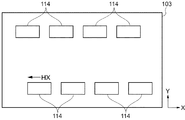
図1(a)に示すように、プラズマ表示装置10はそれぞれがY軸方向に延びる複数のアドレス電極14と、複数のアドレス電極14に信号を与えるアドレス電極駆動回路14Dと、それぞれがX軸方向に延びる複数の表示スキャン電極26と、複数の表示スキャン電極26に信号を与える表示スキャン電極駆動回路26Dと、を備えている。ここでいうX軸方向およびY軸方向は互いに直交する方向であり、後述する吐出装置におけるノズルがステージに対し相対移動する方向と同じである。
As shown in FIG. 1A, the
複数のアドレス電極14は、プラズマ表示装置の背面基板に設けられている。また、複数の表示スキャン電極26は、プラズマ表示装置の前面基板に設けられている。なお、プラズマ表示装置10は、前面基板に設けられた複数の表示電極も備えているが、図1では、説明を平易にする目的で省略されている。背面基板、前面基板、および複数の表示電極については後述する。
The plurality of
図1(b)に示すように、アドレス電極14同士の間隔は、ほぼ300μmである。また、複数のアドレス電極14のそれぞれは、広幅部14Aと、狭幅部14Bと、を有している。広幅部14Aの幅はほぼ20μmである。狭幅部14Bの幅はほぼ5μmである。
本実施例では、複数のアドレス電極14のそれぞれは、狭幅部14Bを介してアドレス電極駆動回路14Dに接続されている。後述するように、アドレス電極14は、基体に設けられた被吐出部18(図8)に、インクジェット装置などの吐出装置を用いて液状の配線材料を吐出することで形成されている。
As shown in FIG. 1B, the interval between the
In the present embodiment, each of the plurality of
本実施例のアドレス電極14は、本発明の「層パターン」または「配線」の一例である。
The
図2に示す製造装置1は、基体における被吐出部18(図8)に配線を形成する装置である。具体的には、製造装置1は、被吐出部18のすべてに液状の配線材料111を塗布する吐出装置100と、被吐出部18上の配線材料111を乾燥させる乾燥装置150と、配線材料111を再度加熱(ポストベーク)するオーブン160と、を備えている。さらに製造装置1は、吐出装置100、乾燥装置150、オーブン160の順番に基体を搬送する搬送装置170も備えている。
The
図3に示すように、吐出装置100は、液状の配線材料111を保持するタンク101と、チューブ110を介してタンク101から配線材料111が供給される吐出走査部102と、を備える。吐出走査部102は、それぞれが液状の配線材料を吐出可能な複数のヘッド114(図4)を有するキャリッジ103と、キャリッジ103の位置を制御する第1位置制御装置104と、支持基板12を保持するステージ106と、ステージ106の位置を制御する第2位置制御装置108と、制御部112と、を備えている。タンク101と、キャリッジ103における複数のヘッド114と、はチューブ110で連結されており、タンク101から複数のヘッド114のそれぞれに液状の配線材料111が圧縮空気によって供給される。
As shown in FIG. 3, the
本実施例における液状の配線材料111は、本発明の「液状の材料」の一例である。液状の材料とは、ノズルから吐出可能な粘度を有する材料をいう。この場合、材料が水性であると油性であるとを問わない。ノズルから吐出可能な流動性(粘度)を備えていれば十分で、固体物質が混入していても全体として流動体であればよい。
The
第1位置制御装置104はリニアモータを備えており、制御部112からの信号に応じて、キャリッジ103をX軸方向、およびX軸方向と直交するZ軸方向に沿って移動させる。第2位置制御装置108はリニアモータを備えており、制御部112からの信号に応じて、X軸方向およびZ軸方向の両方と直交するY軸方向に沿ってステージ106を移動させる。ステージ106はX軸方向およびY軸方向の双方と平行な平面を有していて、この平面上に基体10A(図8)を固定できるように構成されている。ステージ106が基体10Aを固定するので、ステージ106は被吐出部18、18G、18Bの位置を決定できる。なお、本実施例の基体10Aは、受容基板の一例である。
The first
第1位置制御装置104は、さらに、Z軸方向に平行な所定の軸の回りでキャリッジ103を回転させる機能も有する。Z軸方向とは、鉛直方向(つまり重力加速度の方向)に平行な方向である。第1位置制御装置104によるキャリッジ103のZ軸方向に平行な軸の回りの回転によって、受容基板上に固定された座標系におけるX軸およびY軸を、X軸方向およびY軸方向とそれぞれ平行にできる。本実施例では、X軸方向およびY軸方向は、ともにステージ106に対してキャリッジが相対移動する方向である。本明細書では、第1位置制御措置104および第2位置制御装置108を「走査部」と表記することもある。
The first
キャリッジ103およびステージ106は上記以外の平行移動および回転の自由度をさらに有している。ただし、本実施例では、上記自由度以外の自由度に関する記載は説明を平易にする目的で省略されている。
The
制御部112は、配線材料111を吐出すべき相対位置を表す吐出データを外部情報処理装置から受け取るように構成されている。制御部112の詳細な機能は、後述する。
The
図4に示すように、キャリッジ103は、互いに同じ構造を有する複数のヘッド114を保持している。ここで、図4は、キャリッジ103をステージ106側から観察した図であり、このため図面に垂直な方向がZ軸方向である。本実施例では、キャリッジ103には4個のヘッド114からなる列が2列配置されている。それぞれのヘッド114の長手方向とX軸方向との間の角度ANは0°になるように、ヘッド114のそれぞれがキャリッジ103に固定されている。ただし、変形例で説明するように、この角度ANは可変である。
As shown in FIG. 4, the
図5に示すように、配線材料111を吐出するためのヘッド114は、それぞれがヘッド114の長手方向に延びる2つのノズル列116を有している。ノズル列116とは、180個のノズル118が一列に並んだ列のことである。ノズル列116の方向をノズル列方向HXと表記する。ノズル列方向HXに沿ったノズル118の間隔は、約140μmである。また、図5において、1つのヘッド114における2つのノズル列116は、互いに半ピッチ(約70μm)だけ互いにずれて位置している。さらに、ノズル118の直径は、およそ27μmである。上述したように、ヘッド114の長手方向とX軸方向との間の角度が角度ANだから、ノズル列方向HX、すなわち180個のノズル118が一列に並ぶ方向とX軸方向との間の角度も角度ANである。なお、複数のノズル118のそれぞれの端部は、上記X軸方向およびY軸方向で定義される仮想的な平面上に位置している。また、ヘッド114がほぼZ軸と平行に材料を吐出できるように、複数のノズル118のそれぞれの形状が調整されている。
As shown in FIG. 5, the
図6(a)および(b)に示すように、それぞれのヘッド114は、インクジェットヘッドである。より具体的には、それぞれのヘッド114は、振動板126と、ノズルプレート128と、を備えている。振動板126と、ノズルプレート126と、の間には、タンク101から孔131を介して供給される液状の配線材料111が常に充填される液たまり129が位置している。また、振動板126と、ノズルプレート128と、の間には、複数の隔壁122が位置している。そして、振動板126と、ノズルプレート128と、1対の隔壁122と、によって囲まれた部分がキャビティ120である。キャビティ120はノズル118に対応して設けられているため、キャビティ120の数とノズル118の数とは同じである。キャビティ120には、1対の隔壁122の間に位置する供給口130を介して、液たまり129から配線材料111が供給される。
As shown in FIGS. 6A and 6B, each
振動板126上には、それぞれのキャビティ120に対応して、振動子124が位置する。振動子124は、ピエゾ素子124Cと、ピエゾ素子124Cを挟む1対の電極124A、124Bと、を含む。この1対の電極124A、124Bに駆動電圧を与えることで、対応するノズル118から液状の配線材料111が吐出される。
On the
制御部112(図3)は、複数の振動子124のそれぞれに互いに独立な信号を与えるように構成されている。このため、ノズル118から吐出される配線材料111の体積は、制御部112からの信号に応じてノズル118毎に制御される。さらに、ノズル118のそれぞれから吐出される配線材料111の体積は、0pl〜42pl(ピコリットル)の間で可変である。このため、塗布走査の間に吐出動作を行うノズル118と、吐出動作を行わないノズル118と、を設定することでもできる。
The control unit 112 (FIG. 3) is configured to give independent signals to each of the plurality of
本明細書では、1つのノズル118と、ノズル118に対応するキャビティ120と、キャビティに対応する振動子124と、を含んだ部分を、吐出部127と表記することもある。この表記によれば、1つのヘッド114は、ノズル118の数と同じ数の吐出部127を有する。上述のように本実施例では、キャリッジ103はヘッド114を保持する。一方、ヘッド114のそれぞれは複数の吐出部127を有している。このため、本明細書では、キャリッジ103が複数の吐出部127を保持すると表記することもある。
In the present specification, a portion including one
吐出部127は、ピエゾ素子の代わりに電気熱変換素子を有してもよい。つまり、吐出部127は、電気熱変換素子による材料の熱膨張を利用して材料を吐出する構成を有していてもよい。
The
上述のように、キャリッジ103は第1位置制御装置104(図3)によってX軸方向およびZ軸方向に移動させられる。一方、ステージ106(図3)は第2位置制御手段108(図3)によってY軸方向に移動させられる。この結果、第1位置制御装置104および第2位置制御装置108によって、ステージ106に対してキャリッジ103が相対移動する。より具体的には、これらの動作によって、複数のヘッド114、複数のノズル列116、または複数のノズル118は、ステージ106上で位置決めされた被吐出部18に対してZ軸方向に所定の距離を保ちながらX軸方向およびY軸方向に相対的に移動、すなわち相対的に走査する。さらに具体的には、ヘッド114は、ステージに対してX軸方向およびY軸方向に相対走査するとともに、複数のノズル118から材料を吐出する。
本発明では、被吐出部18に対してノズル118をY軸方向に走査して、被吐出部18に対してノズル118から材料を吐出してもよい。「相対走査」とは吐出する側とそこからの吐出物が着弾する側(被吐出部18側)の少なくとも一方を他方に対して走査することを含む。また、相対走査と材料の吐出との組合せを指して「塗布走査」と表記することもある。
As described above, the
In the present invention, the
次に、制御部112の構成を説明する。図7の機能ブロック図に示すように、制御部112は、入力バッファメモリ200と、記憶手段202と、処理部204と、走査ドライバ206と、ヘッドドライバ208と、を備えている。バッファメモリ202と処理部204とは相互に通信可能に接続されている。処理部204と記憶手段202とは、相互に通信可能に接続されている。処理部204と走査ドライバ206とは相互に通信可能に接続されている。処理部204とヘッドドライバ20とは相互に通信可能に接続されている。また、走査ドライバ206は、第1位置制御手段104および第2位置制御手段108と相互に通信可能に接続されている。同様にヘッドドライバ208は、複数のヘッド114のそれぞれと相互に通信可能に接続されている。
Next, the configuration of the
入力バッファメモリ200は、外部情報処理装置から配線材料111の吐出を行うための吐出データを受け取る。吐出データは、基体10A上のすべての被吐出部18の相対位置を表すデータと、すべての被吐出部18に所望の厚さの配線材料111を塗布するまでに必要となる相対走査の回数を示すデータと、被吐出部上の着弾位置を示すデータと、吐出動作を行うノズル118を指定するデータと、吐出動作を行わないノズル118を指定するデータと、を含む。入力バッファメモリ200は、吐出データを処理部204に供給し、処理部204は吐出データを記憶手段202に格納する。図7では、記憶手段202はRAMである。
The
処理部204は、記憶手段202内の吐出データに基づいて、被吐出部18に対するノズル列116の相対位置を示すデータを走査ドライバ206に与える。走査ドライバ206はこのデータに応じた駆動信号を第1位置制御手段104および第2位置制御手段108に与える。この結果、被吐出部18に対してノズル列116が走査される。一方、処理部204は、記憶手段202に記憶された吐出データに基づいて、対応するノズル118からの吐出タイミングを示すデータをヘッドドライバ208に与える。ヘッドドライバ208はこのデータに基づいて、配線材料111の吐出に必要な駆動信号をヘッド114に与える。この結果、ノズル列116における対応するノズル118から液状の配線材料111が吐出される。
The
制御部112は、少なくともCPU、ROM、RAMを含んだコンピュータであってもよい。この場合には、制御部112の上記機能は、コンピュータによって実行されるソフトウェアプログラムによって実現される。もちろん、制御部112は、専用の回路(ハードウェア)によって実現されてもよい。
The
以上の構成によって、吐出装置100Rは、制御部112に与えられた吐出データに応じて、配線材料111の塗布走査を行う。
With the above configuration, the
次に、アドレス電極14の製造方法を説明する。まず、ガラス基板などの支持基板12をUV洗浄する。そして、図8(a)に示すように、支持基板12の一方の面の全面を覆うようにスピンコート法を用いて、黒顔料が分散された熱硬化型アクリル樹脂(すなわち樹脂ブラック)を2μm程度の厚さに塗布する。このことで、支持基板12上に樹脂ブラック層20Aを形成する。さらに樹脂ブラック層20Aの全面を覆うようにフッ素系ポリマーがブレンドされたネガ型のアクリル系化学増幅型感光性レジストを塗布することで、樹脂ブラック層20A上にレジスト層20Bを形成する。
Next, a method for manufacturing the
次に、レジスト層20Bと樹脂ブラック層20Aとをパターニングする。具体的には、図8(b)に示すように、アドレス電極14が形成されるべき領域に対応した部位に遮光部ABを有するフォトマスクPM1を介して、レジスト層20Bに光hνを照射する。そして、所定のエッチング液を用いてエッチングすることで、光hνが照射されていない複数の部分、すなわち複数のアドレス電極14に対応する複数の部分のレジスト層20Bと、樹脂ブラック層20Aと、を取り除く。そのことによって、図8(c)に示すように、後に形成されるべきアドレス電極14を囲む形状を有する樹脂ブラック層20Cとレジスト層20Dとが、支持基板12上に得られる。
Next, the resist
このように、支持基板12上に位置する樹脂ブラック層20Cと樹脂ブラック層20C上に位置するレジスト層20Dとを形成することで、樹脂ブラック層20Cとレジスト層20Dとによって区画された領域(つまり被吐出部18)を支持基板12上に形成する。
本実施例では、樹脂ブラック層20Cが本発明の「第1の層」に対応し、レジスト層20Dが発明の「第2の層」に対応する。
In this manner, by forming the resin
In this embodiment, the resin
本明細書では、このような形状を有する樹脂ブラック層20Cと、樹脂ブラック層20C上に位置するレジスト層20Dとを合わせて、バンク20と表記することもある。この表記によれば、樹脂ブラック層20Cとレジスト層20Dとを含むバンク20を形成することで、バンク20によって区画された領域、すなわち被吐出部18、が支持基板12上に形成される。なお、本実施例において、「バンク」とは、「隔壁」、「仕切り部」などを含む用語である。
In the present specification, the resin
図8(f)に示すように、被吐出部18は、アドレス電極14の形状とほぼ同じ形状を有している。このため、被吐出部18は、アドレス電極14の広幅部14Aに対応する広幅領域18Aと、アドレス電極14の狭幅部14Bに対応する狭幅領域18Bと、を有している。広幅領域18Aの幅は、ほぼ20μmであり、狭幅領域18Bの幅は、ほぼ5μmである。本実施例では、支持基板12と、支持基板12上に形成された被吐出部18と、を合わせて、基体10Aと表記することもある。
As shown in FIG. 8 (f), the discharged
次に、製造装置1における吐出装置100のステージ106上に基体10Aを固定することで、ステージ106上に被吐出部18を位置決めする。この場合、被吐出部18の長手方向がY軸方向と平行になるように、ステージ106上で基体10Aを固定する。そして、ノズル118のX座標が、被吐出部18のX座標に一致するように、キャリッジ103およびステージ106の少なくとも一方を移動させる。この場合、複数のノズル118のX座標のそれぞれが、複数の被吐出部18のX座標に同時に一致するように、ノズル列方向HXとX軸方向との間の角度ANを設定しておくことが好ましい。そうすれば、1つの走査期間の間に、複数の被吐出部18を同時に塗布走査できるからである。
Next, the
図8(d)および(g)に示すように、吐出装置100は、1つの走査期間の間に、対応するノズル118から被吐出部18に液状の配線材料111を吐出する。この場合、図8(d)および(g)に示すように、吐出装置100は、被吐出部18のうち、広幅領域18Aにのみに対して所定の間隔で液状の配線材料111を吐出する。なお、ノズル118から吐出された直後の配線材料の液滴をX軸方向およびY軸方向で決まる平面に投影した場合、その投影された液滴の半径はほぼ20μmである。つまり、液滴の半径は、広幅領域18Aの幅とほぼ同じである。
As shown in FIGS. 8D and 8G, the
ところで、本明細書において「走査期間」とは、キャリッジ103の一辺がY軸方向に沿って走査範囲の一端(または他端)から他端(または一端)まで相対移動を1回行う期間を意味する。さらに、本実施例において「走査範囲」とは、複数の被吐出部18の全てに配線材料111を塗布するまでに、キャリッジ103の一辺が相対移動する範囲を意味する。しかしながら、場合によっては用語「走査範囲」は、1つのノズル118が相対移動する範囲を意味することもあるし、1つのノズル列116が相対移動する範囲を意味することもあるし、1つのヘッド114が相対移動する範囲を意味することもある。なお、キャリッジ103、ヘッド114、またはノズル118が相対移動するとは、被吐出部18に対するこれらの相対位置が変わることである。このため、キャリッジ103、ヘッド114、またはノズル118が絶対静止して、被吐出部18のみがステージ106によって移動する場合であっても、キャリッジ103、ヘッド114、またはノズル118が相対移動すると表現する。
By the way, in this specification, the “scanning period” means a period in which one side of the
液状の配線材料111とは、導電性微粒子を分散媒に分散させた分散液である。導電性微粒子としては、例えば、金、銀、銅、パラジウム、及びニッケルのうちのいずれかを含有する金属微粒子の他、これらの酸化物、並びに導電性ポリマーや超電導体の微粒子などが用いられる。
The
これらの導電性微粒子は、分散性を向上させるために表面に有機物などをコーティングして使うこともできる。導電性微粒子の表面にコーティングするコーティング材としては、例えばキシレン、トルエン等の有機溶剤やクエン酸等が挙げられる。 These conductive fine particles can be used by coating the surface with an organic substance or the like in order to improve dispersibility. Examples of the coating material that coats the surface of the conductive fine particles include organic solvents such as xylene and toluene, citric acid, and the like.
導電性微粒子の粒径は1nm以上0.1μm以下であることが好ましい。0.1μmより大きいと、ノズル118に目詰まりが生じる場合がある。また、1nmより小さいと、導電性微粒子に対するコーテイング剤の体積比が大きくなり、得られる膜中の有機物の割合が過多となり、この結果、導電性が低下する。
The particle diameter of the conductive fine particles is preferably 1 nm or more and 0.1 μm or less. If it is larger than 0.1 μm, the
分散媒としては、上記の導電性微粒子を分散できるもので、凝集を起こさないものであれば特に限定されない。例えば、水の他に、メタノール、エタノール、プロパノール、ブタノールなどのアルコール類、n−ヘプタン、n−オクタン、デカン、ドデカン、テトラデカン、トルエン、キシレン、シメン、デュレン、インデン、ジペンテン、テトラヒドロナフタレン、デカヒドロナフタレン、シクロヘキシルベンゼンなどの炭化水素系化合物、またエチレングリコールジメチルエーテル、エチレングリコールジエチルエーテル、エチレングリコールメチルエチルエーテル、ジエチレングリコールジメチルエーテル、ジエチレングリコールジエチルエーテル、ジエチレングリコールメチルエチルエーテル、1,2−ジメトキシエタン、ビス(2−メトキシエチル)エーテル、p−ジオキサンなどのエーテル系化合物、さらにプロピレンカーボネート、γ−ブチロラクトン、N−メチル−2−ピロリドン、ジメチルホルムアミド、ジメチルスルホキシド、シクロヘキサノンなどの極性化合物を例示できる。これらのうち、微粒子の分散性と分散液の安定性、また液滴吐出法(インクジェット法)への適用の容易さの点で、水、アルコール類、炭化水素系化合物、エーテル系化合物が好ましく、より好ましい分散媒としては、水、炭化水素系化合物を挙げることができる。 The dispersion medium is not particularly limited as long as it can disperse the conductive fine particles and does not cause aggregation. For example, in addition to water, alcohols such as methanol, ethanol, propanol, butanol, n-heptane, n-octane, decane, dodecane, tetradecane, toluene, xylene, cymene, durene, indene, dipentene, tetrahydronaphthalene, decahydro Hydrocarbon compounds such as naphthalene and cyclohexylbenzene, ethylene glycol dimethyl ether, ethylene glycol diethyl ether, ethylene glycol methyl ethyl ether, diethylene glycol dimethyl ether, diethylene glycol diethyl ether, diethylene glycol methyl ethyl ether, 1,2-dimethoxyethane, bis (2- Methoxyethyl) ether, ether compounds such as p-dioxane, propylene carbonate, γ- Butyrolactone, N- methyl-2-pyrrolidone, dimethylformamide, dimethyl sulfoxide, can be exemplified polar compounds such as cyclohexanone. Of these, water, alcohols, hydrocarbon compounds, and ether compounds are preferred from the viewpoints of fine particle dispersibility and dispersion stability, and ease of application to the droplet discharge method (inkjet method). More preferred dispersion media include water and hydrocarbon compounds.
本実施例では、上記の液状の配線材料111に対して、レジスト層20Dは撥液性を呈する。さらに、液状の配線材料111に対する樹脂ブラック層20Cの撥液性は、配線材料111に対するレジスト層20Dの撥液性よりも低い。むしろ、樹脂ブラック層20Cは、液状の配線材料111に対して親液性を呈する。これらの理由は、レジスト層20Dにはフッ素ポリマーがブレンドされており、一方、樹脂ブラック層20Cはフッ素系ポリマーを含有しないからである。一般に、フッ素を含む樹脂の表面は、フッ素を含まない樹脂の表面よりも、上記分散媒を含む配線材料に対して高い撥液性を呈する。一方、フッ素を含まない樹脂の多くは、上記液状の配線材料に対して親液性を示す。
In the present embodiment, the resist
レジスト層20Dが相対的に高い撥液性を呈するため、被吐出部18に着弾した直後の液滴は、レジスト層20Dを超えて被吐出部18の外へ流れず、樹脂ブラック層20Cの方に流れ落ちる。また、支持基板12に近い層、すなわち樹脂バンク層20C、が親液性を呈するため、狭幅領域18Bに配線材料111が吐出されなくても、広幅領域18Aに着弾した配線材料111が狭幅領域18Bに流れ込む。なぜなら、樹脂バンク層20Cによって毛細管現象が生じるからである。さらに、所望の撥液性を示す層と親液性を示す層とからバンク20が形成されているため、バンクを撥液化または親液化するための表面改質工程が不要になる。例えばテトラフルオロメタンを処理がガスとするプラズマ処理や酸素プラズマ処理が不要になる。
Since the resist
本実施例では、液状の材料に対して撥液性を示す層の材料として、フッ素系ポリマーがブレンドされたネガ型のアクリル系化学増幅型感光性レジストを用いている。感光特性は、ネガ型に限定されず、ポジ型であってもよい。また、本実施例では、液状の材料に対して親液性を示す層の材料として、黒顔料が分散された熱硬化型アクリル樹脂(樹脂ブラック)を用いている。しかしながら、樹脂ブラック以外にも、感光性ポリイミド、アクリル系レジスト、エポキシ系レジストが、親液性を示す層として利用できる。 In this embodiment, a negative acrylic chemically amplified photosensitive resist blended with a fluorine-based polymer is used as a material for a layer exhibiting liquid repellency with respect to a liquid material. The photosensitive characteristic is not limited to the negative type, and may be a positive type. Further, in this embodiment, a thermosetting acrylic resin (resin black) in which a black pigment is dispersed is used as a material of a layer showing lyophilicity with respect to a liquid material. However, in addition to resin black, photosensitive polyimide, acrylic resist, and epoxy resist can be used as the lyophilic layer.
なお、分散媒の性質によっては、フッ素ポリマーを含まない材料の方が配線材料111に対して撥液性を呈する場合もある。このような場合には、配線材料に含まれる分散媒に応じて、所望の撥液性と、所望の親液性と、が得られるように、材料を選択すればよい。
Depending on the nature of the dispersion medium, a material that does not contain a fluoropolymer may exhibit liquid repellency with respect to the
以上の吐出方法によって、図8(e)および(h)に示すように、広幅領域18Aだけでなく、狭幅領域18Bにも配線材料の層が塗布される。
With the above discharge method, as shown in FIGS. 8E and 8H, the wiring material layer is applied not only to the
基体10Aの被吐出部18のすべてに配線材料111の層が形成された場合には、搬送装置170が基体10Aを乾燥装置150内に位置させる。そして、被吐出部18上の配線材料111を完全に乾燥させることで、被吐出部18にアドレス電極14を得る。次に搬送装置170は、支持基板12を、オーブン160内に位置させる。その後、オーブン160は複数のアドレス電極14を再加熱(ポストベーク)する。再加熱後の広幅部14Aの厚さおよび狭幅部14Bの厚さは、ともにほぼ2μmである。
When the layer of the
以上の工程によって、支持基板12上に複数のアドレス電極14が形成される。その後、公知の薄膜形成工程やパターニング工程などを利用して、アドレス電極14が形成された基体10Aから、図9に示すプラズマ表示装置10を得る。
Through the above steps, a plurality of
図9は、製造装置1によって製造されたアドレス電極14を備えた プラズマ表示装置10の模式図である。プラズマ表示装置10は、背面基板10Bと、前面基板10Cと、を備えている。
FIG. 9 is a schematic diagram of the
背面基板10Bは、上述の支持基板12と、支持基板12上にストライプ状に形成された複数のアドレス電極14と、アドレス電極14を覆うように形成された誘電体ガラス層16と、格子状の形状を有するとともに複数の画素領域を規定する隔壁21と、を含む。
隔壁21で囲まれるセル(つまり画素領域)には、赤、緑、青のいずれかの光を発光可能な蛍光層17が塗布されている。複数の画素領域はマトリクス状に位置しており、複数の画素領域が形成するマトリクスの列のそれぞれは、複数のアドレス電極14のそれぞれに対応する。
The
A cell (that is, a pixel region) surrounded by the
前面基板10Cは、ガラス基板28と、ガラス基板28上で互いに平行にパターニングされた表示電極25および表示スキャン電極26と、表示電極25および表示スキャン電極26とを覆うように形成された誘電体ガラス層24と、誘電体ガラス層24上に形成されたMgO保護層22と、を有する。背面基板10Bと前面基板10Cとは、背面基板10Bのアドレス電極54と、前面基板10Cの表示電極25・表示スキャン電極26とが、互いに直交するように位置合わせされている。各隔壁21で囲まれるセル(画素領域)には、所定の圧力で放電ガス29が封入されている。なお、図10においては、バンク20は取り除かれているが、バンク20をプラズマ表示装置10内に残してもよい。
The
本実施例では、プラズマ表示装置10におけるアドレス配線14の製造方法を説明したが、本実施例の製造方法がプラズマ表示装置10の表示電極25や表示スキャン電極26など他の配線に適用されても、上述の効果と同様の効果が得られる。
In the present embodiment, the manufacturing method of the
本発明を液晶表示装置の製造方法に適用した例を説明する。なお、以下で説明するように、実施例2の被吐出部の形状と実施例1の被吐出部の形状とが異なる点を除いて、実施例2は実施例1と基本的に同じである。 An example in which the present invention is applied to a method for manufacturing a liquid crystal display device will be described. As described below, the second embodiment is basically the same as the first embodiment except that the shape of the discharged portion of the second embodiment is different from the shape of the discharged portion of the first embodiment. .
図10(a)に示すように、液晶表示装置30はそれぞれがX軸方向に延びる複数のゲート線34と、複数のゲート線34に信号を与えるゲート線駆動回路34Dと、それぞれがY軸方向に延びる複数のソース線46と、複数のソース線46に信号を与えるソース線駆動回路46Dと、複数のスイッチング素子44と、複数の保持容量CPと、複数の画素容量LCと、を備えている。ここでいうX軸方向およびY軸方向は互いに直交しており、実施例1において説明したように、吐出装置100におけるノズル118がステージに対し相対移動する方向と同じである。また、後述するように、複数のゲート線34および複数のソース線46は、液晶表示装置30の素子側基板に設けられている。素子側基板については、後述する。
As shown in FIG. 10A, the liquid
それぞれのスイッチング素子44のゲート電極44Gおよびドレイン電極44Dは、対応するゲート線34およびソース線46にそれぞれ接続されている。また、それぞれのスイッチング素子44のソース電極44Sは、画素容量LCの一部である画素電極36(図12)および保持容量CPの一部である電極の双方に接続されている。
The
図10(b)に示すように、ゲート線34同士の間隔は、ほぼ300μmである。複数のゲート線34のそれぞれは、広幅部34Aと、狭幅部34Bと、を有している。広幅部34Aの幅、すなわち長手方向と直交する方向の長さ、は、狭幅部34Bの幅よりも長い。広幅部34Aはそれぞれのゲート線34における部分のうちのX軸方向に延びるストライプ状の部分である。広幅部34Aの幅はほぼ20μmである。狭幅部34Bは、広幅部34AからY軸方向に突き出た部分であり、スイッチング素子44のゲート電極44Gでもある。狭幅部34Bの幅は、ほぼ10μmである。後述するように、ゲート線34は、基体に設けられた被吐出部38(図11)に、インクジェット装置などの吐出装置を用いて液状の配線材料を吐出することで形成されている。具体的には、ゲート線34は、実施例1で説明した製造装置1(図2)によって形成されている。
As shown in FIG. 10B, the interval between the gate lines 34 is approximately 300 μm. Each of the plurality of
本実施例のゲート電極34は、本発明の「層パターン」または「配線」の一例である。
The
次に、ゲート線34の製造方法を説明する。まず、ガラス基板などの支持基板32をUV洗浄する。そして、図11(a)に示すように、支持基板32の一方の面の全面を覆うように、スピンコート法を用いて黒顔料が分散された熱硬化型アクリル樹脂(すなわち樹脂ブラック)を塗布する。このことで、支持基板32上に樹脂ブラック層40Aを形成する。さらに樹脂ブラック層40Aの全面を覆うようにフッ素系ポリマーがブレンドされたネガ型のアクリル系化学増幅型感光性レジストを塗布することで、樹脂ブラック層40A上にレジスト層40Bを形成する。
Next, a method for manufacturing the
次に、レジスト層40Bと樹脂ブラック層40Aとをパターニングする。具体的には、図11(b)に示すように、ゲート線34が形成されるべき領域に対応した部位に遮光部ABを有するフォトマスクPM2を介して、レジスト層40Bに光hνを照射する。そして、所定のエッチング液を用いてエッチングすることで、光hνが照射されていな複数の部分、すなわち複数のゲート線34に対応する複数の部分のレジスト層40Bと、樹脂ブラック層40Aと、を取り除く。そのことによって、図11(c)に示すように、後に形成されるべきゲート線34を囲む形状を有する樹脂ブラック層40Cとレジスト層40Dとが、支持基板32上に得られる。
Next, the resist
このように、支持基板32上に位置する樹脂ブラック層40Cと樹脂ブラック層40C上に位置するレジスト層40Dとを形成することで、樹脂ブラック層40Cとレジスト層40Dとによって区画された領域(つまり被吐出部38)を支持基板32上に形成する。
本実施例では、樹脂ブラック層40Cが本発明の「第1の層」に対応し、レジスト層40Dが発明の「第2の層」に対応する。
In this way, by forming the resin
In this embodiment, the resin
本明細書では、このような形状を有する樹脂ブラック層40Cと、樹脂ブラック層40C上に位置するレジスト層40Dとを合わせて、バンク40と表記することもある。この表記によれば、樹脂ブラック層40Cとレジスト層40Dとを含むバンク40を形成することで、バンク40によって区画された領域、すなわち被吐出部38、が支持基板32上に形成される。
In this specification, the resin
図11(f)に示すように、被吐出部38は、ゲート線34の形状とほぼ同じ形状を有している。このため、被吐出部38は、ゲート線34の広幅部34Aに対応する広幅領域38Aと、ゲート線34の挟幅部34Bに対応する狭幅領域38Bと、を有している。広幅領域38Aの幅は、ほぼ20μmであり、狭幅領域38Bの幅は、ほぼ10μmである。本実施例では、支持基板32と、支持基板上に形成された被吐出部38と、を合わせて、基体30Aと表記することもある。
As shown in FIG. 11 (f), the discharged
次に、製造装置1における吐出装置100のステージ106上に基体30Aを固定することで、ステージ106上に被吐出部38を位置決めする。この場合、被吐出部38の長手方向がY軸方向と平行になるように、ステージ106上で基体30Aを固定する。そして、ノズル118のX座標が、被吐出部38のX座標に一致するように、キャリッジ103およびステージ106の少なくとも一方を移動させる。この場合、複数のノズル118のX座標のそれぞれが、複数の被吐出部38のX座標に同時に一致するように、ノズル列方向HXとX軸方向との間の角度ANを設定しておくことが好ましい。そうすれば、1つの走査期間の間に、複数の被吐出部38を同時に塗布走査できるからである。
Next, the
なお、被吐出部38の形状に応じて、吐出装置100の制御部112に与えられる吐出データは、実施例1の吐出データから変更されている。
Note that the discharge data given to the
図11(d)および(g)に示すように、吐出装置100は、1つの走査期間の間に、対応するノズル118から被吐出部38に液状の配線材料111を吐出する。この場合、図11(d)および(g)に示すように、吐出装置100は、被吐出部38のうち、広幅領域38Aにのみに対して所定の間隔で液状の配線材料111を吐出する。なお、ノズル118から吐出された直後の配線材料の液滴をX軸方向およびY軸方向で決まる平面に投影した場合、その投影された液滴の半径はほぼ20μmである。つまり、液滴の半径は、広幅領域38Aの幅とほぼ同じである。
As shown in FIGS. 11D and 11G, the
本実施例では、液状の配線材料111に対して、レジスト層40Dは撥液性を呈する。
さらに、液状の配線材料111に対する樹脂ブラック層40Cの撥液性は、配線材料111に対するレジスト層40Dの撥液性よりも低い。むしろ、樹脂ブラック層40Cは、液状の配線材料111に対して親液性を呈する。これらの理由は、レジスト層40Dにはフッ素ポリマーがブレンドされており、一方、樹脂ブラック層40Cはフッ素系ポリマーを含有しないからである。一般に、フッ素を含む樹脂の表面は、フッ素を含まない樹脂の表面よりも、実施例1で説明した分散媒を含む配線材料に対して高い撥液性を呈する。一方、フッ素を含まない樹脂の多くは、上記液状の配線材料に対して親液性を示す。
In the present embodiment, the resist
Furthermore, the liquid repellency of the resin
レジスト層40Dが相対的に高い撥液性を呈するため、被吐出部38に着弾した直後の配線材料111の液滴は、レジスト層40Dを超えて被吐出部38の外へ流れず、樹脂ブラック層40Cの方に流れ落ちる。また、支持基板32に近い層、すなわち樹脂ブラック層40C、が親液性を呈するため、狭幅領域38Bに配線材料が吐出されなくても、狭幅領域38Aに着弾した配線材料111が狭幅領域38Bに流れ込む。なぜなら、樹脂ブラック層40Cによって毛細管現象が生じるからである。さらに、所望の撥液性を示す層と親液性を示す層とからバンク40が形成されているため、バンクを撥液化または親液化するための表面改質工程が不要になる。例えばテトラフルオロメタンを処理がガスとするプラズマ処理や酸素プラズマ処理が不要になる。
Since the resist
本実施例では、液状の材料に対して撥液性を示す層の材料として、フッ素系ポリマーがブレンドされたネガ型のアクリル系化学増幅型感光性レジストを用いている。感光特性は、ネガ型に限定されず、ポジ型であってもよい。また、本実施例では、液状の材料に対して親液性を示す層の材料として、黒顔料が分散された熱硬化型アクリル樹脂を用いている。しかしながら、樹脂ブラック以外にも、感光性ポリイミド、アクリル系レジスト、エポキシ系レジストが、親液性を示す層として利用できる。 In this embodiment, a negative acrylic chemically amplified photosensitive resist blended with a fluorine-based polymer is used as a material for a layer exhibiting liquid repellency with respect to a liquid material. The photosensitive characteristic is not limited to the negative type, and may be a positive type. Further, in this embodiment, a thermosetting acrylic resin in which a black pigment is dispersed is used as a material of a layer showing lyophilicity with respect to a liquid material. However, in addition to resin black, photosensitive polyimide, acrylic resist, and epoxy resist can be used as the lyophilic layer.
なお、分散媒の性質によっては、フッ素ポリマーを含まない材料の方が配線材料111に対して撥液性を呈する場合もある。このような場合には、配線材料に含まれる分散媒に応じて、所望の撥液性と、所望の親液性と、が得られるように、材料を選択すればよい。
Depending on the nature of the dispersion medium, a material that does not contain a fluoropolymer may exhibit liquid repellency with respect to the
以上の吐出方法によって、図11(e)および(h)に示すように、広幅領域38Aだけでなく、狭幅領域38Bにも配線材料の層が塗布される。
By the above discharge method, as shown in FIGS. 11E and 11H, the wiring material layer is applied not only to the
基体30Aの被吐出部38のすべてに配線材料111の層が形成された場合には、搬送装置170が基体30Aを乾燥装置150内に位置させる。そして、被吐出部38上の配線材料111を完全に乾燥させることで、被吐出部38にゲート線34を得る。次に搬送装置170は、基体30Aを、オーブン160内に位置させる。その後、オーブン160は複数のゲート線34を再加熱(ポストベーク)する。再加熱後の広幅部34Aの厚さおよび狭幅部34Bの厚さは、いずれもほぼ2μmである。
When the layer of the
以上の工程によって、基体30A上に複数のゲート線34が形成される。その後、公知の薄膜形成工程やパターニング工程などを利用して、ゲート線34が形成された基体30Aから、図12に示す液晶表示装置30を得る。
Through the above steps, a plurality of
図12は、製造装置1によって製造されたゲート線34を備えた液晶表示装置30の模式図である。液晶表示装置30は、素子側基板30Bと、前面基板30Cと、を備えている。
FIG. 12 is a schematic diagram of the liquid
素子側基板30Bは、支持基板32の第1の面に設けられた偏光板31Pと、支持基板32の第1の面に対向する第2の面上に形成された複数のゲート線34と、複数のゲート線34を覆うように形成された酸化膜33と、酸化膜33と支持基板32とを覆うように形成されたゲート絶縁膜42と、それぞれのゲート電極44Gを覆うようにゲート絶縁膜42上に位置するそれぞれの半導体層35と、を備えている。さらに、素子側基板30Bは、対応する半導体層35上でゲート電極44Gの一部と重なるとともに、ゲート電極44Gに対応する領域上で互いに所定の距離だけ離れて位置するコンタクト層37Sおよびコンタクト層37Dと、コンタクト層37S上に位置するソース電極44Sと、コンタクト層37D上に位置するドレイン電極44Dと、ドレイン電極44Dに接続されたソース線46と、ソース電極44Sとドレイン電極44Dとソース線46を覆う保護膜39と、保護膜39上に位置するポリイミドなどの層間絶縁層45と、層間絶縁層45上でマトリクス状に配置された複数の画素電極36と、複数の画素電極36と層間絶縁層45とを覆う配向膜41Pとを備える。複数の画素電極36は、ITO(Indium-Tin Oxide)などの光透過性を有する材料から形成されている。配向膜41Pには、所定の方向にラビング処理が施されている。ソース電極44Sの一部に対応する部分には、コンタクトホール(不図示)が設けられており、コンタクトホール内の導電性膜を介して画素電極36とソース電極44Sとが接続されている。ゲート電極44G、酸化膜33、半導体層35、一対のコンタクト層37Sとコンタクト層37Dと、ソース電極44S、ドレイン電極44Dは、スイッチング素子44に対応し、画素領域毎に設けられている。なお、複数の画素電極36のそれぞれに対応するそれぞれの領域が、画素領域である。
The element-
前面基板30Cは、ガラス基板などの基板43の第1の面に設けられた偏光板31Sと、基板43の第1の面に対向する第2の面上に位置するとともに、それぞれが複数の画素領域のそれぞれに対応した複数の開口部を有するブラックマトリクス47と、ブラックマトリクス47上に形成されたバンク49Bと、バンク49Bによって仕切られた領域に位置する複数のカラーフィルタ層49Fと、複数のカラーフィルタ層49Fとバンク49Bとを覆うオーバーコート層OCと、オーバコート層OC上に位置するとともに、複数の画素電極36の全てを覆う対向電極36Cと、対向電極36Cを覆う配向膜41Sと、を備えている。配向膜41Sには適切な方向にラビング処理が施されている。なお、配向膜41Pに施されたラビングの方向と、配向膜41Sに施されたラビングの方向とは、配向膜41Pと配向膜41Sとの間で液晶分子が例えばTN(Twisted nematic)配向するように、設定されている。
The
素子側基板30Bと前面基板30Cとの間には、配向層41Pと配向層41Sとに接するように液晶層30Dが位置する。なお、図12においては、バンク40は取り除かれているが、バンク40を液晶表示装置30内に残してもよい。
A
本実施例では、液晶表示装置30におけるゲート線34の製造方法を説明したが、本実施例の製造方法が液晶表示装置30のソース線46や保持容量用配線など他の配線に適用されても、上述の効果と同様の効果が得られる。
In the present embodiment, the manufacturing method of the
(実施例1および2の変形例)
実施例1および2において、プラズマ表示装置の製造方法および液晶表示装置の製造方法をそれぞれ説明した。より具体的には、それぞれの表示装置における配線の製造方法を説明した。ただし、実施例1および2の製造方法は、プラズマ表示装置および液晶表示装置以外の電子機器の製造方法に適用されてもよい。具体的には、電子機器における配線であって、広幅部と狭幅部とを有する配線の製造方法に上記製造方法を適用すれば、実施例1および実施例2において説明した効果と同様な効果が得られる。
(Modification of Examples 1 and 2)
In Examples 1 and 2, the method for manufacturing the plasma display device and the method for manufacturing the liquid crystal display device have been described. More specifically, a method for manufacturing a wiring in each display device has been described. However, the manufacturing methods of
本明細書において「電子機器」とは、プラズマ表示装置、液晶表示装置、エレクトロルミネッセンス表示装置、FED(Field Emission display)やSED(Surface-Conduction Electron-Emitter Display)を含む電子放出素子を備えた画像表示装置などの表示装置だけでなく、ICタグやRFID(Radio Frequency Identification)タグなどの無線タグや、半導体装置なども含む用語である。 In this specification, “electronic device” means an image including a plasma display device, a liquid crystal display device, an electroluminescence display device, an electron emission element including a field emission display (FED) and a surface-conduction electron-emitter display (SED). It is a term that includes not only a display device such as a display device but also a wireless tag such as an IC tag and an RFID (Radio Frequency Identification) tag, a semiconductor device, and the like.
本発明をエレクトロルミネッセンス表示装置の製造装置に適用した例を説明する。 An example in which the present invention is applied to an electroluminescence display device manufacturing apparatus will be described.
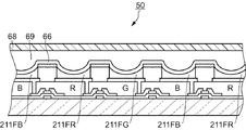
図13(a)および(b)に示す基体50Aは、後述する製造装置2(図14)による処理によって、エレクトロルミネッセンス表示装置50となる基板である。基体50Aは、マトリクス状に配置された複数の被吐出部58R、58G、58Bを有する。
A
具体的には、基体50Aは、支持基板52と、支持基板52上に形成された回路素子層54と、回路素子層54上に形成された複数の画素電極56と、複数の画素電極56の間に形成されたバンク60と、を有している。支持基板52は、可視光に対して光透過性を有する基板であり、例えばガラス基板である。複数の画素電極56のそれぞれは、可視光に対して光透過性を有する電極であり、例えば、ITO(Indium-Tin Oxide)電極である。また、複数の画素電極56は、回路素子層54上にマトリクス状に配置されており、それぞれが画素領域を規定する。そして、バンク60は、格子状の形状を有しており、複数の画素電極56のそれぞれを囲む。また、バンク60は、回路素子層54上に形成された樹脂ブラック層60Cと、樹脂ブラック層60C上に位置するレジスト層60Dとからなる。
Specifically, the
回路素子層54は、支持基板52上で所定の方向に延びる複数の走査電極と、複数の走査電極を覆うように形成された絶縁膜62と、絶縁膜62上に位置するともに複数の走査電極が延びる方向に対して直交する方向に延びる複数の信号電極と、走査電極および信号電極の交点付近に位置する複数のスイッチング素子64と、複数のスイッチング素子64を覆うように形成されたポリイミドなどの層間絶縁層65と、を有する層である。それぞれのスイッチング素子64のゲート電極64Gおよびドレイン電極64Dは、それぞれ対応する走査電極および対応する信号電極と電気的に接続されている。層間絶縁層65上には複数の画素電極56が位置する。層間絶縁層65には、各スイッチング素子64のソース電極64Sに対応する部位にスルーホール64Vが設けられており、このスルーホール64V内の導電性膜を介して、スイッチング素子64と、対応する画素電極56と、が接続されている。また、バンク60に対応する位置にそれぞれのスイッチング素子64が位置している。つまり、図20(b)の紙面に垂直な方向から観察すると、複数のスイッチング素子64のそれぞれは、バンク60に覆われるように位置している。
The
基体50Aの画素電極56とバンク60とで規定される凹部(画素領域の一部)は、被吐出部58R、被吐出部58G、被吐出部58Bに対応する。被吐出部58Rは、赤の波長域の光線を発光する発光層211FRが形成されるべき領域であり、被吐出部58Gは、緑の波長域の光線を発光する発光層211FGが形成されるべき領域であり、被吐出部58Bは、青の波長域の光線を発光する発光層211FBが形成されるべき領域である。
A concave portion (a part of the pixel region) defined by the
本実施例の発光層211FR、211FG、211FBは、本発明の「層パターン」の一例である。 The light emitting layers 211FR, 211FG, and 211FB in this example are examples of the “layer pattern” in the present invention.
図13(b)に示す基体50Aは、X軸方向およびY軸方向で規定される仮想平面と平行に位置している。そして、複数の被吐出部58R,58G、58Bが形成するマトリクスの行方向および列方向は、それぞれX軸方向およびY軸方向と平行である。基体50Aにおいて、被吐出部58R、被吐出部58G、および被吐出部58Bは、X軸方向にこの順番で周期的に並んでいる。一方、被吐出部58R同士はY軸方向に所定の間隔をおいて1列に並んでおり、また、被吐出部58G同士はY軸方向に所定の間隔をおいて1列に並んでおり、同様に、被吐出部58B同士はY軸方向に所定の間隔をおいて1列に並んでいる。
The
被吐出部58R同士のX軸方向に沿った間隔LRXは、ほぼ560μmである。この間隔は、被吐出部58G同士のX軸方向に沿った間隔LGXと同じであり、被吐出部18B同士のX軸方向に沿った間隔LBXとも同じである。また、被吐出部58RのX軸方向の長さはほぼ100μmであり、Y軸方向の長さはほぼ300μmである。被吐出部58Gおよび被吐出部58Bも被吐出部58Rと同じ大きさを有している。被吐出部同士の上記間隔および被吐出部の上記大きさは、40インチ程度の大きさのハイビジョンテレビにおいて、同一色に対応する画素領域同士の間隔に対応する。
An interval LRX along the X-axis direction between the discharged
図14に示す製造装置2は、図13の基体50Aの被吐出部58R,58G、58Bのそれぞれに対して、対応する発光材料を吐出する装置である。製造装置2は、被吐出部58Rのすべてに発光材料211Rを塗布する吐出装置200Rと、被吐出部58R上の発光材料211Rを乾燥させる乾燥装置250Rと、被吐出部58Gのすべてに発光材料211Gを塗布する吐出装置200Gと、被吐出部58G上の発光材料211Gを乾燥させる乾燥装置250Gと、被吐出部58Bのすべてに発光材料211Bを塗布する吐出装置200Bと、被吐出部58B上の発光材料Bを乾燥させる乾燥装置250Bと、を備えている。さらに製造装置2は、吐出装置200R、乾燥装置250R、吐出装置200G、乾燥装置250G、吐出装置200B、乾燥装置250Bの順番に基体50Aを搬送する搬送装置270も備えている。
The
図15に示す吐出装置200Rは、液状の発光材料211Rを保持するタンク201Rと、チューブ210Rを介してタンク201Rから発光材料211Rが供給される吐出走査部102と、を備える。吐出走査部102の構成は、実施例1の吐出走査部102(図3)の構成と同じであるため、同様な構成要素には同一の参照符号を付けるとともに、重複する説明を省略する。また、吐出装置200Gの構成と吐出装置200Bの構成とは、どちらも基本的に吐出装置200Rの構造と同じある。ただし、吐出装置200Rにおけるタンク201Rの代わりに、吐出装置200Gが発光材料211G用のタンクを備える点で吐出装置200Gの構成は吐出装置200Rの構成と異なる。同様に、タンク201Rの代わりに、吐出装置200Bが発光材料201B用のタンクを備える点で吐出装置200Bの構成は吐出装置200Rの構成と異なる。
A
製造装置2を用いたエレクトロルミネッセンス表示装置50の製造方法を説明する。まず、公知の製膜技術とパターニング技術とを用いて、支持基板52上に回路素子層54を形成し、その後、回路素子層54上に複数の画素電極56をマトリクス状に形成する。
A method for manufacturing the
まず、回路素子層54上および画素電極56上をUV洗浄する。そして、図16(a)に示すように、回路素子層54上および画素電極56を覆うようにスピンコート法を用いて、黒顔料が分散された熱硬化型アクリル樹脂(すなわち樹脂ブラック)を塗布する。このことで、回路素子層54上および画素電極56上に樹脂ブラック層60Aを形成する。
さらに樹脂ブラック層60Aの全面を覆うようにフッ素系ポリマーがブレンドされたネガ型のアクリル系化学増幅型感光性レジストを塗布することで、樹脂ブラック層60A上にレジスト層60Bを形成する。なお、本実施例では、回路素子層54および画素電極56を含む部分を「回路基板」と表記することもある。
First, UV cleaning is performed on the
Further, by applying a negative acrylic chemically amplified photosensitive resist blended with a fluorine polymer so as to cover the entire surface of the resin
次に、レジスト層60Bと樹脂ブラック層60Aとをパターニングする。具体的には、図16(b)に示すように、発光層211FR、211FG、211FBが形成されるべき領域に対応する部位に遮光部ABを有するフォトマスクPM3を介して、レジスト層24Bに光hνを照射する。そして、所定のエッチング液を用いてエッチングすることで、光hνが照射されていない部分、すなわち発光層211FR、211FG、211FBに対応する部分のレジスト層60Bと、対応する樹脂ブラック層60Aとを取り除く。そのことによって、図16(c)に示すように、後に形成されるべき発光層211FR、211FG,211FBを囲む形状を有する樹脂ブラック層60Cとレジスト層60Dとが、回路基板上に得られる。
Next, the resist
このように、回路基板上に位置する樹脂ブラック層60Cと樹脂ブラック層60C上に位置するレジスト層60Dとを形成することで、樹脂ブラック層60Cとレジスト層60Dとによって区画された領域(つまり被吐出部58R、58G、58B)を前記基板上に形成する。本実施例では、樹脂ブラック層60Cが本発明の「第1の層」に対応し、レジスト層60Dが発明の「第2の層」に対応する。
In this way, by forming the resin
本明細書では、このような形状を有する樹脂ブラック層60Cと、樹脂ブラック層60C上に位置するレジスト層60Dとを合わせて、バンク60と表記することもある。この表記によれば、樹脂ブラック層60Cとレジスト層60Dとを含むバンク60を形成することで、バンク60によって区画された領域、すなわち被吐出部58R、58G、58Bが回路基板上に形成される。
In the present specification, the resin
被吐出部58R,58G、58Bにおける画素電極56の上に、対応する正孔輸送層57R、57G、57Bを形成してもよい。正孔輸送層57R、57G、57Bが、画素電極上56と、後述の発光層211RF、211GF、211BFと、の間に位置すれば、エレクトロルミネッセンス表示装置の発光効率が高くなる。画素電極56の上に正孔輸送層57R、57G、57Bを設ける場合には、正孔輸送層57R、57G、57Bと、バンク60と、によって規定された凹部が、被吐出部58R、58G、58Bに対応する。
Corresponding
なお、正孔輸送層57R、57G、57Bをインクジェット法により形成することも可能である。つまり、吐出装置200を用いて、正孔輸送層37R、37G、37Bを被吐出部58R,58G、58Bに設けてもよい。この場合、正孔輸送層57R、57G、57Bを形成するための材料を含む溶液を各画素領域ごとに所定量塗布し、その後、乾燥させることにより正孔輸送層57R、57G、57Bを形成することができる。
Note that the
被吐出部58R,58G、58Bを有する基体50Aは、搬送装置270によって、吐出装置200Rのステージ106に運ばれる。そして、図16(d)に示すように、吐出装置200Rは、被吐出部58Rのすべてに発光材料211Rの層が形成されるように、ヘッド114から発光材料211Rを吐出する。基体50Aの被吐出部58Rのすべてに発光材料211Rの層が形成された場合には、搬送装置270が基体50Aを乾燥装置250R内に位置させる。そして、被吐出部58R上の発光材料211Rを完全に乾燥させることで、被吐出部58R上に発光層211FRを得る。
The
次に搬送装置270は、基体50Aを吐出装置200Gのステージ106に位置させる。そして、吐出装置200Gは、被吐出部58Gのすべてに発光材料211Gの層が形成されるように、ヘッド114から発光材料Gを吐出する。基体50Aの被吐出部58Gのすべてに発光材料211Gの層が形成された場合には、搬送装置270が基体50Aを乾燥装置250G内に位置させる。そして、被吐出部58G上の発光材料Gを完全に乾燥させることで、被吐出部58G上に発光層211FGを得る。
Next, the
次に搬送装置270は、基体50Aを吐出装置200Bのステージ106に位置させる。そして、吐出装置200Bは、被吐出部58Bのすべてに発光材料211Bの層が形成されるように、ヘッド114から発光材料Bを吐出する。基体50Aの被吐出部58Bのすべてに発光材料Bの層が形成された場合には、搬送装置270が基体50Aを乾燥装置250B内に位置させる。そして、被吐出部58B上の発光材料211Bを完全に乾燥させることで、被吐出部58B上に発光層211FBを得る。
Next, the
本実施例では、液状の発光材料211R、211G、211Bに対して、レジスト層60Dは撥液性を呈する。さらに、液状の発光材料211R、211G、211Bに対する樹脂ブラック層60Cの撥液性は、発光材料211R、211G、211Bに対するレジスト層60Dの撥液性よりも低い。むしろ、樹脂ブラック層60Cは、液状の発光材料211R、211G、211Bに対して親液性を呈する。これらの理由は、レジスト層60Dにはフッ素ポリマーがブレンドされており、一方、樹脂ブラック層60Cはフッ素系ポリマーを含有しないからである。一般に、フッ素を含む樹脂の表面は、フッ素を含まない樹脂の表面よりも、上記分散媒を含む配線材料に対して高い撥液性を呈する。一方、フッ素を含まない樹脂の多くは、上記液状の配線材料に対して親液性を示す。
In the present embodiment, the resist
レジスト層60Dが相対的に高い撥液性を呈するため、被吐出部58R、58G、58Bに着弾した直後の発光材料の液滴は、レジスト層60Dを超えて被吐出部58R、58G、58Bの外へ流れず、樹脂ブラック層60Cの方に流れ落ちる。さらに、所望の撥液性を示す層と親液性を示す層とからバンク60が形成されているため、バンクを撥液化または親液化するための表面改質工程が不要になる。例えばテトラフルオロメタンを処理がガスとするプラズマ処理や酸素プラズマ処理が不要になる。
Since the resist
次に、図17に示すように発光層211FR,211FG、211FB、およびバンク60を覆うように対向電極66を設ける。対向電極66は陰極として機能する。その後、封止基板68と基体50Aとを、互いの周辺部で接着することで、図17に示すエレクトロルミネッセンス表示装置50が得られる。なお、封止基板68と基体50Aとの間には不活性ガス69が封入されている。
Next, as shown in FIG. 17, the
エレクトロルミネッセンス表示装置50において、発光層211FR、211FG、211FBから発光した光は、画素電極56と、回路素子層54と、支持基板52と、を介して射出する。このように回路素子層54を介して光を射出するエレクトロルミネッセンス表示装置は、ボトムエミッション型の表示装置と呼ばれる。
In the
上記実施例において、第1の層、第2の層を積層した構造による隔壁の例を示したが、第1の層のみにより形成することも可能である。 In the above-described embodiment, an example of a partition wall having a structure in which the first layer and the second layer are stacked has been described. However, it is also possible to form the partition only by the first layer.
すなわち、第1の層のみで隔壁を形成し、隔壁の親液性/撥液性の度合いをコントロールすることにより、前述の実施例1乃至3の構造と類似する構造を得ることができる。 That is, by forming the partition only with the first layer and controlling the degree of lyophilicity / liquid repellency of the partition, a structure similar to the structure of the first to third embodiments can be obtained.
例えば、撥液処理する際、隔壁の下層部分を親液性が高くなるように、隔壁の上層部分を下層部分よりも撥液性が高くなるように(すなわち撥液性とする)、処理することにより達成することができる。 For example, when the liquid repellent treatment is performed, the lower layer portion of the partition wall is processed so that the lyophilic property is higher, and the upper layer portion of the partition wall is higher in liquid repellency than the lower layer portion (that is, liquid repellency). Can be achieved.
従って、1層の隔壁により形成したとしても、幅の広い領域へ液滴を塗布することにより、幅の狭い領域へ塗布した液が浸透し、線幅の狭い領域へも液を充填させることができる。隔壁の材料は前述に示したような材料を用いることができる。 Therefore, even if it is formed by a single-layer partition wall, by applying droplets to a wide area, the liquid applied to a narrow area can penetrate and fill the liquid to a narrow line area. it can. The material as described above can be used for the material of the partition wall.
更には、線幅の広い領域を塗布する際は、線幅方向に複数滴の液滴を滴下することにより描画することもできる。このような描画方法をとることにより、配線幅が広い領域への塗布が早くできるとともに、充填も早くできる。更に、充填を早く行うことができるため、線幅の狭い領域への液の充填も早く行うことができる。 Furthermore, when a region having a wide line width is applied, drawing can be performed by dropping a plurality of droplets in the line width direction. By adopting such a drawing method, application to a wide wiring width region can be made faster and filling can be made faster. Furthermore, since the filling can be performed quickly, the liquid can be quickly filled into the region having a narrow line width.
また、膜厚を厚く形成したい場合は、前述のような描画を複数回行うことができる。具体的には、図示されているような描画を複数回行うこと、更には前述のように線幅方向に複数的の液滴が滴下されるような描画方法を複数回行うこと、ができる。 In addition, when it is desired to form a thick film, the above-described drawing can be performed a plurality of times. Specifically, the drawing as shown in the figure can be performed a plurality of times, and further, the drawing method in which a plurality of droplets are dropped in the line width direction as described above can be performed a plurality of times.
以上のような描画方法は前述に記載の実施例1乃至3のいずれにも適用可能である。 The above drawing method can be applied to any of the first to third embodiments described above.
1・2…製造装置
10A…基体
10B…背面基板
10C…前面基板
12…支持基板
14…アドレス電極
14A…広幅部
14B…狭幅部
14D…アドレス電極駆動回路
18…被吐出部
18A…広幅領域
18B…狭幅領域
16…誘電体ガラス層
20…バンク
20A・20C…樹脂ブラック層
20B・20D…レジスト層
21…隔壁
22…MgO(酸化マグネシウム)保護層
24…誘電体ガラス層、25…表示電極
26…表示スキャン電極
28…ガラス基板
29…放電ガス
30…液晶表示装置
30A…基体
30B…素子側基板
30C…前面基板
30D…液晶層
31P・31S…偏光板
33…酸化膜
34…ゲート線
34A…広幅部
34B…狭幅部
34D…ゲート線駆動回路
35…半導体層
36…画素電極
36C…対向電極
37S・37D…コンタクト層
38A…広幅領域
38B…狭幅領域
39…保護膜
40…バンク
40A・40C…樹脂ブラック層
40B・40D…レジスト層
41P・41S…配向膜
42…ゲート絶縁膜
43…基板
44…スイッチング素子
44G…ゲート電極
44S…ソース電極
44D…ドレイン電極
44V…コンタクトホール
45…層間絶縁層
46…ソース線
46D…ソース線駆動回路
47…ブラックマトリクス
49B…バンク
49F…カラーフィルタ層
50A…基体
50…エレクトロルミネッセンス表示装置
52…支持基板
54…回路素子層
56…画素電極
57R、57G、57B…正孔輸送層
58R、58G、58B…被吐出部
60…バンク、60A・60C…樹脂ブラック層
60B・60D…レジスト層
62…絶縁膜
64…スイッチング素子
65…層間絶縁層
64G…ゲート電極
64S…ソース電極
64D…ドレイン電極
64V…スルーホール
66…対向電極
68…封止基板
69…不活性ガス
101…タンク
102…吐出走査部
103…キャリッジ
104…第1位置制御装置
108…第2位置制御装置
100…吐出装置
106…ステージ
110…チューブ
111…配線材料
112…制御部
114…ヘッド
116…ノズル列
118…ノズル
126…振動板
128…ノズルプレート
131…孔
129…液たまり
122…隔壁
120…キャビティ
124…振動子
124C…ピエゾ素子
124A・124B…電極
127…吐出部
130…供給口
150…乾燥装置
160…オーブン
170…搬送装置
211R・211G・211B…発光材料
211FR・211FG・211FB…発光層
1 ... 2 ...
Claims (6)
前記第1の層と前記第2の層とによって区画された領域を前記基板上に形成するステップ
(a)と、
吐出装置の吐出部から前記領域に液状の材料を吐出するステップ(b)と、
を含み、
前記液状の材料に対する前記第1の層の撥液性は、前記材料に対する前記第2の層の撥
液性よりも低く、
前記ステップ(a)は、前記領域が、前記吐出された液状の材料の直径と同じもしくは
広い第1の幅を有する第1の部分と前記吐出された液状の材料の直径よりも狭い第2の幅
を有する第2の部分と、を有するように、前記第1の層と前記第2の層を形成するステッ
プを含み、
前記ステップ(b)は、前記第1の部分に前記材料を吐出し、前記第1の部分から前記
第2の部分に前記材料を流れ込ませるステップを含む、
層パターン製造方法。 Forming a first layer located on the substrate and a second layer located on the first layer;
Forming on the substrate a region defined by the first layer and the second layer;
A step (b) of discharging a liquid material from the discharge portion of the discharge device to the region;
Including
Liquid repellency of the first layer to the material of the liquid, rather lower than the liquid repellent property of the second layer with respect to the material,
In the step (a), the area is the same as the diameter of the discharged liquid material or
A first portion having a wide first width and a second width narrower than the diameter of the discharged liquid material
A step of forming the first layer and the second layer so as to have a second portion.
Including
In the step (b), the material is discharged to the first portion, and the first portion
Allowing the material to flow into a second portion;
Layer pattern manufacturing method.
前記第1の層は、前記液状の材料に対して親液性を有する、
層パターン製造方法。 It is a layer pattern manufacturing method of Claim 1, Comprising:
The first layer is lyophilic with respect to the liquid material.
Layer pattern manufacturing method.
前記第1の層と前記第2の層とによって区画された領域を前記基板上に形成するステップ
(a)と、
吐出装置の吐出部から前記領域に液状の配線材料を吐出するステップ(b)と、
を含み、
前記液状の配線材料に対する前記第1の層の撥液性は、前記配線材料に対する前記第2
の層の撥液性よりも低く、
前記ステップ(a)は、前記領域が、前記吐出された液状の材料の直径と同じもしく
は広い第1の幅を有する第1の部分と前記吐出された液状の材料の直径よりも狭い第2の
幅を有する第2の部分と、を有するように、前記第1の層と前記第2の層を形成するステ
ップを含み、
前記ステップ(b)は、前記第1の部分に前記材料を吐出し、前記第1の部分から前記
第2の部分に前記材料を流れ込ませるステップを含む、
配線製造方法。 Forming a first layer located on the substrate and a second layer located on the first layer;
Forming on the substrate a region defined by the first layer and the second layer;
A step (b) of discharging a liquid wiring material from the discharge portion of the discharge device to the region;
Including
The liquid repellency of the first layer with respect to the liquid wiring material is the second level with respect to the wiring material.
Lower than the liquid repellency of the layer of
In the step (a), the region may have the same diameter as the discharged liquid material.
Is a first portion having a wide first width and a second portion that is narrower than the diameter of the discharged liquid material.
A step of forming the first layer and the second layer so as to have a second portion having a width.
Including
In the step (b), the material is discharged to the first portion, and the first portion
Allowing the material to flow into a second portion;
Wiring manufacturing method.
前記第1の層は、前記液状の配線材料に対して親液性を有する、
配線製造方法。 The wiring manufacturing method according to claim 3,
The first layer is lyophilic with respect to the liquid wiring material.
Wiring manufacturing method.
前記第1の層と前記第2の層とによって区画された領域を前記基板上に形成するステップ
(a)と、
吐出装置の吐出部から前記領域に液状の材料を吐出するステップ(b)と、
を含み、
前記液状の材料に対する前記第1の層の撥液性は、前記材料に対する前記第2の層の撥
液性よりも低く、
前記ステップ(a)は、前記領域が、前記吐出された液状の材料の直径と同じもしくは
広い第1の幅を有する第1の部分と前記吐出された液状の材料の直径よりも狭い第2の幅
を有する第2の部分と、を有するように、前記第1の層と前記第2の層を形成するステッ
プを含み、
前記ステップ(b)は、前記第1の部分に前記材料を吐出し、前記第1の部分から前記
第2の部分に前記材料を流れ込ませるステップを含む、
電子機器の製造方法。 Forming a first layer located on the substrate and a second layer located on the first layer;
Forming on the substrate a region defined by the first layer and the second layer;
A step (b) of discharging a liquid material from the discharge portion of the discharge device to the region;
Including
The liquid repellency of the first layer with respect to the liquid material is lower than the liquid repellency of the second layer with respect to the material,
In the step (a), the area is the same as the diameter of the discharged liquid material or
A first portion having a wide first width and a second width narrower than the diameter of the discharged liquid material
A step of forming the first layer and the second layer so as to have a second portion.
Including
In the step (b), the material is discharged to the first portion, and the first portion
Allowing the material to flow into a second portion;
Manufacturing method of electronic equipment.
前記第1の層は、前記液状の材料に対して親液性を有する、
電子機器の製造方法。 A method of manufacturing an electronic device according to claim 5,
The first layer is lyophilic with respect to the liquid material.
Manufacturing method of electronic equipment.
Priority Applications (5)
| Application Number | Priority Date | Filing Date | Title |
|---|---|---|---|
| JP2003327997A JP4192737B2 (en) | 2003-07-15 | 2003-09-19 | Layer pattern manufacturing method, wiring manufacturing method, electronic device manufacturing method |
| TW093119213A TW200510943A (en) | 2003-07-15 | 2004-06-29 | Method for manufacturing layer pattern, wiring and electronic equipment |
| US10/887,822 US7387903B2 (en) | 2003-07-15 | 2004-07-12 | Method for manufacturing layer pattern, method for manufacturing wiring, and method for manufacturing electronic equipment |
| KR1020040054443A KR100613158B1 (en) | 2003-07-15 | 2004-07-13 | Method for manufacturing layer pattern, method for manufacturing wiring, and method for manufacturing electronic equipment |
| CNB2004100638610A CN100479633C (en) | 2003-07-15 | 2004-07-13 | Layered pattern producing method, distribution producing method and method for producing electronic equipment |
Applications Claiming Priority (2)
| Application Number | Priority Date | Filing Date | Title |
|---|---|---|---|
| JP2003274705 | 2003-07-15 | ||
| JP2003327997A JP4192737B2 (en) | 2003-07-15 | 2003-09-19 | Layer pattern manufacturing method, wiring manufacturing method, electronic device manufacturing method |
Related Child Applications (1)
| Application Number | Title | Priority Date | Filing Date |
|---|---|---|---|
| JP2007273501A Division JP2008060600A (en) | 2003-07-15 | 2007-10-22 | Method of manufacturing layer pattern, method of manufacturing wiring, and method of manufacturing electronic device |
Publications (2)
| Publication Number | Publication Date |
|---|---|
| JP2005046828A JP2005046828A (en) | 2005-02-24 |
| JP4192737B2 true JP4192737B2 (en) | 2008-12-10 |
Family
ID=34197131
Family Applications (1)
| Application Number | Title | Priority Date | Filing Date |
|---|---|---|---|
| JP2003327997A Expired - Fee Related JP4192737B2 (en) | 2003-07-15 | 2003-09-19 | Layer pattern manufacturing method, wiring manufacturing method, electronic device manufacturing method |
Country Status (5)
| Country | Link |
|---|---|
| US (1) | US7387903B2 (en) |
| JP (1) | JP4192737B2 (en) |
| KR (1) | KR100613158B1 (en) |
| CN (1) | CN100479633C (en) |
| TW (1) | TW200510943A (en) |
Families Citing this family (13)
| Publication number | Priority date | Publication date | Assignee | Title |
|---|---|---|---|---|
| JP2006179213A (en) | 2004-12-21 | 2006-07-06 | Seiko Epson Corp | Pattern forming substrate, electrooptical device, and manufacturing method of electrooptical device |
| JP2007027588A (en) * | 2005-07-20 | 2007-02-01 | Seiko Epson Corp | Method of forming film pattern, device, electrooptical apparatus, and electronic equipment |
| JP2007053333A (en) * | 2005-07-20 | 2007-03-01 | Seiko Epson Corp | Method of forming film pattern, device, electro-optical device, electronic equipment, and method of manufacturing active matrix substrate |
| JP4677937B2 (en) * | 2005-07-20 | 2011-04-27 | セイコーエプソン株式会社 | Film pattern forming method, device, electro-optical device, electronic apparatus, and active matrix substrate manufacturing method |
| JP4670596B2 (en) * | 2005-11-04 | 2011-04-13 | セイコーエプソン株式会社 | Film pattern forming method, device, electro-optical device, and electronic apparatus |
| JP2007178885A (en) * | 2005-12-28 | 2007-07-12 | Az Electronic Materials Kk | Pattern, wiring pattern and method for manufacturing the same |
| US20070205896A1 (en) * | 2006-03-02 | 2007-09-06 | Axcess International Inc. | System and Method for Determining Location, Directionality, and Velocity of RFID Tags |
| JP2007286469A (en) | 2006-04-19 | 2007-11-01 | Seiko Epson Corp | Method of forming film pattern, method of manufacturing active matrix substrate, device, electrooptical apparatus and electronic device |
| JP2008016413A (en) * | 2006-07-10 | 2008-01-24 | Canon Inc | Manufacturing method of wiring board, manufacturing method of electron source, manufacturing method of image display device, and image reproduction device |
| JP4222390B2 (en) * | 2006-07-25 | 2009-02-12 | セイコーエプソン株式会社 | PATTERN FORMATION METHOD AND LIQUID CRYSTAL DISPLAY DEVICE MANUFACTURING METHOD |
| US8211782B2 (en) * | 2009-10-23 | 2012-07-03 | Palo Alto Research Center Incorporated | Printed material constrained by well structures |
| US8468680B2 (en) | 2010-08-24 | 2013-06-25 | Roche Diagnostics Operations, Inc. | Biosensor test member and method for making the same |
| CN111876020B (en) * | 2020-08-06 | 2021-11-05 | 中国科学院长春应用化学研究所 | Organic luminescent material ink, preparation method thereof and ink-jet printing method |
Family Cites Families (9)
| Publication number | Priority date | Publication date | Assignee | Title |
|---|---|---|---|---|
| JP2000216330A (en) | 1999-01-26 | 2000-08-04 | Seiko Epson Corp | Stacked semiconductor device and its manufacture |
| TW490997B (en) | 2000-03-31 | 2002-06-11 | Seiko Epson Corp | Method of manufacturing organic EL element, and organic EL element |
| JP2002237383A (en) | 2000-03-31 | 2002-08-23 | Seiko Epson Corp | Manufacturing method of organic el element and organic el element |
| JP2002023783A (en) * | 2000-07-13 | 2002-01-25 | Fujitsu Ltd | Conversation processing system |
| JP4308522B2 (en) * | 2000-11-17 | 2009-08-05 | ティーピーオー ディスプレイズ コーポレイション | Organic electroluminescent device and manufacturing method thereof |
| JP2003124210A (en) | 2001-10-15 | 2003-04-25 | Seiko Epson Corp | Surface treatment method, semiconductor device, electric circuit, display module, color filter and light emitting element |
| JP2003163084A (en) | 2001-11-26 | 2003-06-06 | Seiko Epson Corp | Organic el device, manufacturing method therefor, and electronic apparatus |
| US6677251B1 (en) * | 2002-07-29 | 2004-01-13 | Taiwan Semiconductor Manufacturing Co., Ltd | Method for forming a hydrophilic surface on low-k dielectric insulating layers for improved adhesion |
| JP4170049B2 (en) * | 2002-08-30 | 2008-10-22 | シャープ株式会社 | Pattern forming substrate and pattern forming method |
-
2003
- 2003-09-19 JP JP2003327997A patent/JP4192737B2/en not_active Expired - Fee Related
-
2004
- 2004-06-29 TW TW093119213A patent/TW200510943A/en not_active IP Right Cessation
- 2004-07-12 US US10/887,822 patent/US7387903B2/en not_active Expired - Fee Related
- 2004-07-13 KR KR1020040054443A patent/KR100613158B1/en active IP Right Grant
- 2004-07-13 CN CNB2004100638610A patent/CN100479633C/en not_active Expired - Fee Related
Also Published As
| Publication number | Publication date |
|---|---|
| KR20050008493A (en) | 2005-01-21 |
| CN100479633C (en) | 2009-04-15 |
| US7387903B2 (en) | 2008-06-17 |
| CN1578598A (en) | 2005-02-09 |
| JP2005046828A (en) | 2005-02-24 |
| TW200510943A (en) | 2005-03-16 |
| TWI297619B (en) | 2008-06-11 |
| KR100613158B1 (en) | 2006-08-17 |
| US20050042850A1 (en) | 2005-02-24 |
Similar Documents
| Publication | Publication Date | Title |
|---|---|---|
| KR100726272B1 (en) | Pattern formed structure, method of forming pattern, device, electrooptical device and electronic equipment | |
| US7455389B2 (en) | Ejecting method and ejecting apparatus | |
| US7101440B2 (en) | Ejecting method and ejecting apparatus | |
| KR100907737B1 (en) | Dispensing method of liquid body, manufacturing method of wiring board, manufacturing method of color filter, manufacturing method of organic EL light emitting element | |
| US7784425B2 (en) | Droplet ejecting apparatus, electro-optic device, electronic apparatus, and droplet ejecting method | |
| JP4192737B2 (en) | Layer pattern manufacturing method, wiring manufacturing method, electronic device manufacturing method | |
| US8366232B2 (en) | Method of measuring landed dot, measuring apparatus for landed dot, liquid droplet ejection apparatus, method of manufacturing electro-optic apparatus, electro-optic apparatus, and electronic apparatus | |
| KR100615479B1 (en) | Method of manufacturing electro-optical panel and method of manufacturing electronic device, electro-optical panel, electro-optical apparatus, and electronic device | |
| JP2004160449A (en) | Device manufacturing equipment and device manufacturing method, electronic instrument | |
| KR20040012481A (en) | Droplet discharge apparatus, manufacturing method of electric optical apparatus, electric optical apparatus and electronic equipment | |
| US8037841B2 (en) | Liquid droplet ejection apparatus, method for manufacturing electro-optical apparatus, electro-optical apparatus, and electronic apparatus | |
| JP2008094044A (en) | Head unit, droplet discharge device, discharge method of liquid matter, manufacturing method of color filter, manufacturing method of organic el element and manufacturing method of wiring board | |
| US7185966B2 (en) | Detection apparatus and detecting method, droplet discharge apparatus and droplet discharge method, device and electronic equipment | |
| US20060088700A1 (en) | Apparatus for ejecting liquid droplet, work to be applied thereto, method of manufacturing electro-optic device, electro-optic device, and electronic equipment | |
| JP2004295092A (en) | Manufacturing method for electrooptical panel, manufacturing method for electronic equipment, color filter protective film material for electrooptical panel, electrooptical panel, electrooptical apparatus, and electronic equipment | |
| JP5187124B2 (en) | Liquid material discharge method, color filter manufacturing method, and organic EL device manufacturing method | |
| JP4458075B2 (en) | Layer forming method, active matrix substrate manufacturing method, and multilayer wiring substrate manufacturing method | |
| JP2008060600A (en) | Method of manufacturing layer pattern, method of manufacturing wiring, and method of manufacturing electronic device | |
| JP2005349385A (en) | Droplet discharge device, electro-optical device, electronic device, and droplet discharging method | |
| JP2007130572A (en) | Method and system for treating work, method of manufacturing electro-optical device, electro-optical device and electronic equipment | |
| JP2005285616A (en) | Thin film forming method, manufacturing method for electro-optical device, manufacturing method for color filter, and liquid droplet discharging device | |
| JP2010015005A (en) | Method for producing color filter, color filter, method for forming optical element, optical element,electro-optical apparatus and electronic device | |
| JP2006080179A (en) | Forming method of wiring pattern and forming method of source electrode as well as drain electrode for tft | |
| JP2008080276A (en) | Liquid object supply method, device fabrication method, wiring substrate production method, color filter production method, and method of manufacturing organic el apparatus | |
| JP2005319424A (en) | Liquid droplet discharge device, electro-optical device, and electronic equipment |
Legal Events
| Date | Code | Title | Description |
|---|---|---|---|
| A621 | Written request for application examination |
Free format text: JAPANESE INTERMEDIATE CODE: A621 Effective date: 20050727 |
|
| A977 | Report on retrieval |
Free format text: JAPANESE INTERMEDIATE CODE: A971007 Effective date: 20070802 |
|
| A131 | Notification of reasons for refusal |
Free format text: JAPANESE INTERMEDIATE CODE: A131 Effective date: 20070821 |
|
| A521 | Request for written amendment filed |
Free format text: JAPANESE INTERMEDIATE CODE: A523 Effective date: 20071022 |
|
| A131 | Notification of reasons for refusal |
Free format text: JAPANESE INTERMEDIATE CODE: A131 Effective date: 20080408 |
|
| A521 | Request for written amendment filed |
Free format text: JAPANESE INTERMEDIATE CODE: A523 Effective date: 20080417 |
|
| TRDD | Decision of grant or rejection written | ||
| A01 | Written decision to grant a patent or to grant a registration (utility model) |
Free format text: JAPANESE INTERMEDIATE CODE: A01 Effective date: 20080826 |
|
| A01 | Written decision to grant a patent or to grant a registration (utility model) |
Free format text: JAPANESE INTERMEDIATE CODE: A01 |
|
| A61 | First payment of annual fees (during grant procedure) |
Free format text: JAPANESE INTERMEDIATE CODE: A61 Effective date: 20080908 |
|
| R150 | Certificate of patent or registration of utility model |
Ref document number: 4192737 Country of ref document: JP Free format text: JAPANESE INTERMEDIATE CODE: R150 Free format text: JAPANESE INTERMEDIATE CODE: R150 |
|
| FPAY | Renewal fee payment (event date is renewal date of database) |
Free format text: PAYMENT UNTIL: 20111003 Year of fee payment: 3 |
|
| FPAY | Renewal fee payment (event date is renewal date of database) |
Free format text: PAYMENT UNTIL: 20121003 Year of fee payment: 4 |
|
| FPAY | Renewal fee payment (event date is renewal date of database) |
Free format text: PAYMENT UNTIL: 20121003 Year of fee payment: 4 |
|
| FPAY | Renewal fee payment (event date is renewal date of database) |
Free format text: PAYMENT UNTIL: 20131003 Year of fee payment: 5 |
|
| S531 | Written request for registration of change of domicile |
Free format text: JAPANESE INTERMEDIATE CODE: R313531 |
|
| R350 | Written notification of registration of transfer |
Free format text: JAPANESE INTERMEDIATE CODE: R350 |
|
| LAPS | Cancellation because of no payment of annual fees |