JP2008016413A - Manufacturing method of wiring board, manufacturing method of electron source, manufacturing method of image display device, and image reproduction device - Google Patents
Manufacturing method of wiring board, manufacturing method of electron source, manufacturing method of image display device, and image reproduction device Download PDFInfo
- Publication number
- JP2008016413A JP2008016413A JP2006189282A JP2006189282A JP2008016413A JP 2008016413 A JP2008016413 A JP 2008016413A JP 2006189282 A JP2006189282 A JP 2006189282A JP 2006189282 A JP2006189282 A JP 2006189282A JP 2008016413 A JP2008016413 A JP 2008016413A
- Authority
- JP
- Japan
- Prior art keywords
- groove
- wiring
- manufacturing
- region
- substrate
- Prior art date
- Legal status (The legal status is an assumption and is not a legal conclusion. Google has not performed a legal analysis and makes no representation as to the accuracy of the status listed.)
- Withdrawn
Links
Images


Classifications
-
- H—ELECTRICITY
- H01—ELECTRIC ELEMENTS
- H01J—ELECTRIC DISCHARGE TUBES OR DISCHARGE LAMPS
- H01J1/00—Details of electrodes, of magnetic control means, of screens, or of the mounting or spacing thereof, common to two or more basic types of discharge tubes or lamps
- H01J1/02—Main electrodes
- H01J1/30—Cold cathodes, e.g. field-emissive cathode
-
- H—ELECTRICITY
- H01—ELECTRIC ELEMENTS
- H01J—ELECTRIC DISCHARGE TUBES OR DISCHARGE LAMPS
- H01J9/00—Apparatus or processes specially adapted for the manufacture, installation, removal, maintenance of electric discharge tubes, discharge lamps, or parts thereof; Recovery of material from discharge tubes or lamps
- H01J9/02—Manufacture of electrodes or electrode systems
-
- H—ELECTRICITY
- H01—ELECTRIC ELEMENTS
- H01J—ELECTRIC DISCHARGE TUBES OR DISCHARGE LAMPS
- H01J1/00—Details of electrodes, of magnetic control means, of screens, or of the mounting or spacing thereof, common to two or more basic types of discharge tubes or lamps
- H01J1/02—Main electrodes
- H01J1/30—Cold cathodes, e.g. field-emissive cathode
- H01J1/316—Cold cathodes, e.g. field-emissive cathode having an electric field parallel to the surface, e.g. thin film cathodes
-
- H—ELECTRICITY
- H01—ELECTRIC ELEMENTS
- H01J—ELECTRIC DISCHARGE TUBES OR DISCHARGE LAMPS
- H01J31/00—Cathode ray tubes; Electron beam tubes
- H01J31/08—Cathode ray tubes; Electron beam tubes having a screen on or from which an image or pattern is formed, picked up, converted, or stored
- H01J31/10—Image or pattern display tubes, i.e. having electrical input and optical output; Flying-spot tubes for scanning purposes
- H01J31/12—Image or pattern display tubes, i.e. having electrical input and optical output; Flying-spot tubes for scanning purposes with luminescent screen
-
- H—ELECTRICITY
- H05—ELECTRIC TECHNIQUES NOT OTHERWISE PROVIDED FOR
- H05K—PRINTED CIRCUITS; CASINGS OR CONSTRUCTIONAL DETAILS OF ELECTRIC APPARATUS; MANUFACTURE OF ASSEMBLAGES OF ELECTRICAL COMPONENTS
- H05K3/00—Apparatus or processes for manufacturing printed circuits
- H05K3/10—Apparatus or processes for manufacturing printed circuits in which conductive material is applied to the insulating support in such a manner as to form the desired conductive pattern
- H05K3/12—Apparatus or processes for manufacturing printed circuits in which conductive material is applied to the insulating support in such a manner as to form the desired conductive pattern using thick film techniques, e.g. printing techniques to apply the conductive material or similar techniques for applying conductive paste or ink patterns
- H05K3/1258—Apparatus or processes for manufacturing printed circuits in which conductive material is applied to the insulating support in such a manner as to form the desired conductive pattern using thick film techniques, e.g. printing techniques to apply the conductive material or similar techniques for applying conductive paste or ink patterns by using a substrate provided with a shape pattern, e.g. grooves, banks, resist pattern
-
- H—ELECTRICITY
- H05—ELECTRIC TECHNIQUES NOT OTHERWISE PROVIDED FOR
- H05K—PRINTED CIRCUITS; CASINGS OR CONSTRUCTIONAL DETAILS OF ELECTRIC APPARATUS; MANUFACTURE OF ASSEMBLAGES OF ELECTRICAL COMPONENTS
- H05K3/00—Apparatus or processes for manufacturing printed circuits
- H05K3/46—Manufacturing multilayer circuits
- H05K3/4685—Manufacturing of cross-over conductors
-
- H—ELECTRICITY
- H05—ELECTRIC TECHNIQUES NOT OTHERWISE PROVIDED FOR
- H05K—PRINTED CIRCUITS; CASINGS OR CONSTRUCTIONAL DETAILS OF ELECTRIC APPARATUS; MANUFACTURE OF ASSEMBLAGES OF ELECTRICAL COMPONENTS
- H05K2203/00—Indexing scheme relating to apparatus or processes for manufacturing printed circuits covered by H05K3/00
- H05K2203/11—Treatments characterised by their effect, e.g. heating, cooling, roughening
- H05K2203/1173—Differences in wettability, e.g. hydrophilic or hydrophobic areas
-
- H—ELECTRICITY
- H05—ELECTRIC TECHNIQUES NOT OTHERWISE PROVIDED FOR
- H05K—PRINTED CIRCUITS; CASINGS OR CONSTRUCTIONAL DETAILS OF ELECTRIC APPARATUS; MANUFACTURE OF ASSEMBLAGES OF ELECTRICAL COMPONENTS
- H05K3/00—Apparatus or processes for manufacturing printed circuits
- H05K3/0011—Working of insulating substrates or insulating layers
- H05K3/0017—Etching of the substrate by chemical or physical means
-
- H—ELECTRICITY
- H05—ELECTRIC TECHNIQUES NOT OTHERWISE PROVIDED FOR
- H05K—PRINTED CIRCUITS; CASINGS OR CONSTRUCTIONAL DETAILS OF ELECTRIC APPARATUS; MANUFACTURE OF ASSEMBLAGES OF ELECTRICAL COMPONENTS
- H05K3/00—Apparatus or processes for manufacturing printed circuits
- H05K3/10—Apparatus or processes for manufacturing printed circuits in which conductive material is applied to the insulating support in such a manner as to form the desired conductive pattern
- H05K3/107—Apparatus or processes for manufacturing printed circuits in which conductive material is applied to the insulating support in such a manner as to form the desired conductive pattern by filling grooves in the support with conductive material
-
- Y—GENERAL TAGGING OF NEW TECHNOLOGICAL DEVELOPMENTS; GENERAL TAGGING OF CROSS-SECTIONAL TECHNOLOGIES SPANNING OVER SEVERAL SECTIONS OF THE IPC; TECHNICAL SUBJECTS COVERED BY FORMER USPC CROSS-REFERENCE ART COLLECTIONS [XRACs] AND DIGESTS
- Y10—TECHNICAL SUBJECTS COVERED BY FORMER USPC
- Y10T—TECHNICAL SUBJECTS COVERED BY FORMER US CLASSIFICATION
- Y10T29/00—Metal working
- Y10T29/49—Method of mechanical manufacture
- Y10T29/49002—Electrical device making
- Y10T29/49117—Conductor or circuit manufacturing
- Y10T29/49124—On flat or curved insulated base, e.g., printed circuit, etc.
- Y10T29/49128—Assembling formed circuit to base
-
- Y—GENERAL TAGGING OF NEW TECHNOLOGICAL DEVELOPMENTS; GENERAL TAGGING OF CROSS-SECTIONAL TECHNOLOGIES SPANNING OVER SEVERAL SECTIONS OF THE IPC; TECHNICAL SUBJECTS COVERED BY FORMER USPC CROSS-REFERENCE ART COLLECTIONS [XRACs] AND DIGESTS
- Y10—TECHNICAL SUBJECTS COVERED BY FORMER USPC
- Y10T—TECHNICAL SUBJECTS COVERED BY FORMER US CLASSIFICATION
- Y10T29/00—Metal working
- Y10T29/49—Method of mechanical manufacture
- Y10T29/49002—Electrical device making
- Y10T29/49117—Conductor or circuit manufacturing
- Y10T29/49124—On flat or curved insulated base, e.g., printed circuit, etc.
- Y10T29/4913—Assembling to base an electrical component, e.g., capacitor, etc.
-
- Y—GENERAL TAGGING OF NEW TECHNOLOGICAL DEVELOPMENTS; GENERAL TAGGING OF CROSS-SECTIONAL TECHNOLOGIES SPANNING OVER SEVERAL SECTIONS OF THE IPC; TECHNICAL SUBJECTS COVERED BY FORMER USPC CROSS-REFERENCE ART COLLECTIONS [XRACs] AND DIGESTS
- Y10—TECHNICAL SUBJECTS COVERED BY FORMER USPC
- Y10T—TECHNICAL SUBJECTS COVERED BY FORMER US CLASSIFICATION
- Y10T29/00—Metal working
- Y10T29/49—Method of mechanical manufacture
- Y10T29/49002—Electrical device making
- Y10T29/49117—Conductor or circuit manufacturing
- Y10T29/49124—On flat or curved insulated base, e.g., printed circuit, etc.
- Y10T29/49155—Manufacturing circuit on or in base
- Y10T29/49163—Manufacturing circuit on or in base with sintering of base
-
- Y—GENERAL TAGGING OF NEW TECHNOLOGICAL DEVELOPMENTS; GENERAL TAGGING OF CROSS-SECTIONAL TECHNOLOGIES SPANNING OVER SEVERAL SECTIONS OF THE IPC; TECHNICAL SUBJECTS COVERED BY FORMER USPC CROSS-REFERENCE ART COLLECTIONS [XRACs] AND DIGESTS
- Y10—TECHNICAL SUBJECTS COVERED BY FORMER USPC
- Y10T—TECHNICAL SUBJECTS COVERED BY FORMER US CLASSIFICATION
- Y10T29/00—Metal working
- Y10T29/49—Method of mechanical manufacture
- Y10T29/49002—Electrical device making
- Y10T29/49117—Conductor or circuit manufacturing
- Y10T29/49124—On flat or curved insulated base, e.g., printed circuit, etc.
- Y10T29/49155—Manufacturing circuit on or in base
- Y10T29/49165—Manufacturing circuit on or in base by forming conductive walled aperture in base
Abstract
Description
本発明は、配線基板の製造方法、電子源の製造方法、画像表示装置の製造方法、画像再生装置に関する。 The present invention relates to a method for manufacturing a wiring board, a method for manufacturing an electron source, a method for manufacturing an image display device, and an image reproducing device.
電子放出素子を用いたフラットパネルディスプレイでは、マトリクス状に配列された多数の配線(マトリクス配線)の各交差部またはその近傍に望けられた電子放出素子に選択的に電圧をかけることにより、各電子放出素子からの電子放出を制御し、画像を表示する。マトリクス配線は、走査信号が印加される走査配線と、走査配線と交差し変調信号が印加される信号配線とで構成される。近年、より高精細な画像を表示することのできるディスプレイが求められている。そのため、配線はより細線化する必要がある一方で、細線化による配線の抵抗の増加を避けるために配線の膜厚を大きくする必要があった。また、より簡易に作成することのできるディスプレイが求められている。 In a flat panel display using electron-emitting devices, by selectively applying a voltage to each electron-emitting device desired at or near each intersection of a large number of wires arranged in a matrix (matrix wiring), The electron emission from the electron-emitting device is controlled to display an image. The matrix wiring is composed of a scanning wiring to which a scanning signal is applied and a signal wiring that crosses the scanning wiring and to which a modulation signal is applied. In recent years, a display capable of displaying a higher-definition image has been demanded. Therefore, it is necessary to make the wiring thinner, while it is necessary to increase the thickness of the wiring in order to avoid an increase in wiring resistance due to the thinning. There is also a need for a display that can be created more easily.
これらの要求に対する解決策の一つとして、特許文献1及び特許文献2は基板表面に設けた溝内に導電性ペーストを配置し焼成することで溝内に配線を埋め込み、溝の傍に設けられた電子放出素子と接続して駆動する技術を開示している。
しかしながら、基板の表面に設けた溝の内部に導電性ペースト(配線材料を含むペースト)を印刷し、これを焼成することで溝の内部に配線を設ける方法では、焼成時における配線材料の焼結収縮等により、配線と溝の内壁との間に隙間が発生してしまう場合があった。隙間が発生すると、溝の傍の基板表面上に設けられた電極(電子放出素子と接続する電極あるいは電子放出素子を構成する電極)と、溝内部の配線との接続について信頼性が低下する場合があった。また、隙間を小さくしようと導電性ペーストで、完全に溝内を充填してしまうと、温度が大きく変動した場合、基板材料と配線材料の熱膨張係数の差により、溝内に充填した配線が溝の内壁を押し広げ、基板にクラックや割れを生じさせることがあった。溝の傍に位置する基板表面上に設けられた電極と溝内に設けられた配線との接続の信頼性を向上することが求められていた。 However, in the method in which a conductive paste (paste containing a wiring material) is printed inside the groove provided on the surface of the substrate and the wiring is provided inside the groove by firing this, the wiring material is sintered at the time of firing. In some cases, a gap is generated between the wiring and the inner wall of the groove due to shrinkage or the like. When a gap occurs, reliability of the connection between the electrode (the electrode connected to the electron-emitting device or the electrode constituting the electron-emitting device) provided on the substrate surface near the groove and the wiring inside the groove decreases. was there. In addition, if the gap is completely filled with the conductive paste to reduce the gap, if the temperature fluctuates greatly, the wiring filled in the groove may be caused by the difference in the thermal expansion coefficient between the substrate material and the wiring material. In some cases, the inner wall of the groove was expanded to cause cracks or cracks in the substrate. It has been demanded to improve the reliability of connection between an electrode provided on the substrate surface located beside the groove and a wiring provided in the groove.
本発明の目的は、溝の内部に設けられた配線と溝の傍に位置する基板表面上に設けられた電極との接続の信頼性を向上した配線基板の製造方法を提供するものである。 An object of the present invention is to provide a method of manufacturing a wiring board in which the reliability of the connection between the wiring provided inside the groove and the electrode provided on the substrate surface located beside the groove is improved.
(1)本発明は上記目的を達成するため、(A)溝と溝に隣接する領域とを備えた基板と、(B)第1の部分と前記第1の部分から延在する第2の部分とを備えた第1の配線と、を具備し、前記第1の部分が前記溝内に設けらており、前記第2の部分が前記溝に隣接
する領域の一部の上に設けられている、配線基板の製造方法であって、溝を備える基板を用意し、前記第2の部分が設けられる、前記溝に隣接する領域の一部の接触角と、当該一部を前記溝と囲む、前記溝に隣接する領域の他の一部の接触角とを異ならせた後に、少なくとも前記溝内および前記溝に隣接する領域の一部上に導電性ペーストを設ける、ことを特徴とする。
(1) To achieve the above object, the present invention provides (A) a substrate having a groove and a region adjacent to the groove, and (B) a first portion and a second portion extending from the first portion. A first wiring having a portion, wherein the first portion is provided in the groove, and the second portion is provided on a part of a region adjacent to the groove. A method for manufacturing a wiring board, comprising: preparing a substrate having a groove; and providing the second portion, a part of a contact angle of a region adjacent to the groove, and the part being the groove. The conductive paste is provided at least in the groove and on a part of the region adjacent to the groove after making the contact angle of the other part of the region adjacent to the groove different from the surrounding angle. .
(2)また、本発明は、(A)溝と溝に隣接する領域とを備えた基板と、(B)第1の部分と前記第1の部分から延在する第2の部分とを備えた第1の配線と、を具備し、前記第1の部分が前記溝内に設けらており、前記第2の部分が前記溝に隣接する領域の一部の
上に設けられている、配線基板の製造方法であって、 溝を備える基板を用意し、前記第2の部分が設けられる、前記溝に隣接する領域の一部の接触角と、当該一部を挟む、前記溝に隣接する領域の他の一部の接触角とを異ならせた後に、少なくとも前記溝内および前記溝に隣接する領域の一部上に導電性ペーストを設ける、ことを特徴とする。
(2) The present invention also includes (A) a substrate including a groove and a region adjacent to the groove, and (B) a first portion and a second portion extending from the first portion. A first wiring, wherein the first part is provided in the groove, and the second part is provided on a part of a region adjacent to the groove. A method of manufacturing a substrate, comprising: preparing a substrate having a groove; and providing a second contact portion, a contact angle of a part of a region adjacent to the groove, and sandwiching the part, adjacent to the groove. After making the contact angle of another part of the region different, a conductive paste is provided at least in the groove and on a part of the region adjacent to the groove.
(3)また、本発明は、第1の配線および第2の配線を基板に備えた配線基板と、該配線基板上に配置され、前記第1の配線に接続する第1の電極と前記第2の配線に接続する第2の電極とを有する複数の電子放出素子と、を備えた電子源の製造方法であって、前記配線基板を(1)または(2)に記載の配線基板の製造方法により製造することを特徴とする。 (3) Further, the present invention provides a wiring board provided with a first wiring and a second wiring on a board, a first electrode disposed on the wiring board and connected to the first wiring, and the first wiring A method of manufacturing an electron source comprising: a plurality of electron-emitting devices each having a second electrode connected to a second wiring, wherein the wiring substrate is manufactured according to (1) or (2). It is manufactured by the method.
(4)また、本発明は、電子源と、該電子源から放出された電子が照射されることで発光する発光体とを備える画像表示装置の製造方法であって、電子源が(3)に記載の電子源の製造方法により製造されることを特徴とする。 (4) Moreover, this invention is a manufacturing method of an image display apparatus provided with an electron source and the light-emitting body which light-emits by being irradiated with the electron discharge | released from this electron source, Comprising: It is manufactured by the manufacturing method of the electron source described in 1.
(5)また、本発明は、放送信号および電気通信回線を経由した信号の少なくとも一方を受信する受信装置と該受信装置に接続した画像表示装置とを少なくとも備える画像再生装置であって、画像表示装置が(4)に記載の画像表示装置の製造方法により製造されることを特徴とする。 (5) Further, the present invention is an image reproduction device including at least a receiving device that receives at least one of a broadcast signal and a signal that passes through a telecommunication line, and an image display device that is connected to the receiving device. The apparatus is manufactured by the method for manufacturing an image display apparatus according to (4).
溝の内部に設けられた配線と溝の傍に位置する基板表面上に設けられた電極との接続を簡易に且つ信頼性高く行うことができる。 Connection between the wiring provided inside the groove and the electrode provided on the substrate surface located beside the groove can be performed easily and with high reliability.
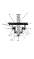
以下に本発明の配線基板(配線を備えた基板)の製造方法の一例を図9を用いて説明する。尚、ここでは、配線基板を電子源へ適用した例を合わせて説明する。図9は、配線基板及び電子源の製造工程を示す図である。 An example of a method for manufacturing a wiring board (a board provided with wiring) according to the present invention will be described below with reference to FIG. Here, an example in which the wiring board is applied to an electron source will be described. FIG. 9 is a diagram showing a manufacturing process of the wiring board and the electron source.
尚、ここでは、電子放出素子として表面伝導型電子放出素子を用いた例を示す。表面伝導型電子放出素子は、間隙を備える導電性膜と当該導電性膜の両端に接続された一対の電極とから構成される。本発明の電子源に用いることのできる電子放出素子としては、電界放出型電子放出素子、MIM型電子放出素子など、少なくとも2つの電極を備える電子放出素子が挙げられる。また、本発明の製造方法で形成することのできる配線基板は、液晶ディスプレイや、有機ELディスプレイやプラズマディスプレイなど、様々なディスプレイの基板1に用いることができる。また、本発明の配線基板上に、上述した電子放出素子や、EL素子や、TFTなどの機能素子を配置し、第1の導体と接続すれば、ディスプレイや回路などの様々な電子デバイスを構成することができる。
Here, an example in which a surface conduction electron-emitting device is used as the electron-emitting device is shown. The surface conduction electron-emitting device includes a conductive film having a gap and a pair of electrodes connected to both ends of the conductive film. Examples of the electron-emitting device that can be used in the electron source of the present invention include an electron-emitting device having at least two electrodes, such as a field-emission electron-emitting device and an MIM-type electron-emitting device. Moreover, the wiring board that can be formed by the manufacturing method of the present invention can be used for the
<配線基板及び電子源の製造方法>
(工程1)
まず、基板1を用意し、基板1の表面の所定箇所にX方向に延在する溝2を多数形成する(図9(A))。尚、ここでは、X方向を図9の紙面に向かって左右方向で示したが、上下方向(Y方向)に溝2を設けることもできる。即ち、溝の延在する方向は所定の方向であれば良い。
<Manufacturing method of wiring board and electron source>
(Process 1)
First, the
基板1の材料としては、絶縁性材料であればよく、特にはガラスが好ましい。勿論、予
め溝2が設けられた基板を利用してもよい。
The material of the
溝2の形成方法としては、ウエットエッチングやドライエッチングなど公知の手法を用いることができるが、サンドブラスト法を用いることが好ましい。サンドブラスト法で形成した溝2の内壁は凹凸を多数備えるため、導電性ペーストの溝2内への充填を効果的に行うことができ、また、後の焼成工程を経て得られた配線4と溝2の内壁との間の干渉(応力の発生など)を抑制することができるので好ましい。
As a method for forming the
(工程2)
次いで、溝2の傍に位置する(溝2に隣接する)基板1の表面(領域)上に一対の電極であるところの第1の電極91と第2の電極92とを設ける(図9(B))。
(Process 2)
Next, a
電極(91、92)の材料としては導電性材料であればよい。例えば、電極(91、92)の材料として、金属材料を用いることができる。特には白金などの化学的に安定な金属材料を用いるのが好ましい。一対の電極の製造方法としては、例えば、スパッタ法などの従来公知の成膜方法を用いることができる。 The material of the electrodes (91, 92) may be any conductive material. For example, a metal material can be used as the material of the electrodes (91, 92). In particular, it is preferable to use a chemically stable metal material such as platinum. As a method for manufacturing the pair of electrodes, for example, a conventionally known film forming method such as a sputtering method can be used.
また、工程2を行う前に、基板1の表面上に酸化シリコンからなる膜を、少なくとも電子放出素子が配置される領域に設けておくことが好ましい。また、基板1の溝2が形成された面の全面に形成してもよい。酸化シリコン膜はスパッタリング法などによって形成することができる。酸化シリコン膜を形成することで、一対の電極91,92上に形成される電子放出素子に有害なナトリウムなどのアルカリ金属が基板1から拡散することを防ぐことできる。尚、酸化シリコン膜を形成する行程は、省略してもよい。
In addition, before performing
(工程3)
次に、溝2(第1の領域711)に隣接する領域の一部であって、配線の主要部分(配線の第1部分)4から延在する部分(配線の第2部分)5が設けられる第2の領域712の接触角と、少なくとも、第2の領域712を挟み、溝2に隣接する領域の他の一部(配線(第1部分4及び第2部分5)が設けられない領域)720の接触角と、を異ならせる。具体的には、基板1の溝2(第1の領域711)以外の表面上であって、配線の第2部分5が設けられない領域(第2部分5の周囲の領域)720の接触角よりも、基板1の表面上であって、第2部分5が設けられる領域712の接触角を低くする(図9(C))。尚、好ましくは、基板1の表面を構成する第1の領域711と第2の領域712の接触角は、配線の第2部分5が設けられない領域(第2部分5の周囲の領域、または第3の領域
)720の接触角よりも低く設定される。そして、特に好ましくは、基板1の表面を構成する第1の領域711と第2の領域712の接触角は同じに設定される。例えば、実用的な値の一例としては、図4(B)の例においては、配線が形成される領域710(第1の領域711および第2の領域712)の接触角を6°とし、配線が形成されない領域(3、720)の接触角を50°とする。ここで、上記「接触角」は、配線(第1部分4および第2部分5)を形成するための導電性ペーストの溶剤(主溶媒)の基板1に対する接触角で定義することができる。ここで示す例では、第2部分5が電極91と接続する必要があるため、第2の領域712は、その一部に、電極91の一部を含む。即ち、第2部分5と接続する部分(第2部分5の一部が覆う部分)における電極91の接触角は、配線の第2部分5が設けられない領域(第2部分5の周囲の領域、または第3の領域)720の接
触角よりも低く設定される。そして好ましくは、第2部分5と接続する部分(第2部分5の一部が覆う部分)における電極91の接触角は、第1の領域711の接触角と実質的に同じに設定される。
(Process 3)
Next, a portion (second portion of the wiring) 5 extending from the main portion (first portion of the wiring) 4 of the wiring, which is a part of the region adjacent to the groove 2 (first region 711), is provided. The contact angle of the
尚、基板1の表面の一部であって、配線(第1部分4および第2部分5)が設けられる領域710は、実質的に溝2の内部に相当する第1の領域(配線の第1部分4が設けられ
る領域)711と、溝2の内部に位置する領域から分岐して延在する第2の領域(配線の第2部分5が設けられる領域)712(本発明の「流路部分」に相当)とで少なくとも構成される。尚、第1の領域711は溝2の内部と同じに設定されることが望ましいが、多少その大きさが異なっていても良い。
Note that a
第1の領域711には、第2の領域712に比べて多量の導電性ペーストが次工程で供給される(投入される)。そのため、導電性ペースト自体の重みで導電性ペーストは溝2内(第1の領域711上)に自然に広がっていく。そして、第1の領域711上を自然に広がっていく導電性ペーストを基板1の第2の領域712上に選択的に広がらせる(流入させる)ために、基板1の第2の領域712の接触角を、典型的には、基板1の第1の領域711及び第2の領域を除いた領域である第3の領域720の接触角よりも低くすればよい。図9(C)では、基板1の表面を、第1の領域711と第2の領域712と第3の領域713のみで構成した例を示したが、その他の領域が存在しても良い。特に、第3の領域720の役割は、少なくとも、第1の領域711からの導電性ペーストの広がりを制御するためのものである。そのため、第3の領域720は、第1の領域711から第2の領域712に導電性ペーストが選択的に分岐されるように設ければ良い(導電性ペーストの流路を規定すればよい)。一般に、導電性ペーストの粘度はそれほど低いものではない。そのため、実用的には、配線の第2の部分5が第1の部分4から分岐して延在する方向(図9ではY方向)とは交差する方向(典型的には直交する方向(図9ではX方向))において第2の領域712を挟むように、第3の領域720を設ければよい。勿論、導電性ペーストのX方向およびY方向における広がりを確実に規定するために、本発明は、図9(C)に示すように、第2の領域712の周囲を第1の領域711(「溝2」と換言する事も出来る)と第3の領域720とで取り囲むことが好ましい。換言すると、本発明は、第1の領域711を、第2の領域712と第3の領域720とで取り囲むことが好ましい。あるいは、また、本発明は、第1の領域711(基板1の表面を構成する領域であって溝2を構成する領域(「溝」とも言う))と第2の領域712(基板1の表面を構成する領域であって溝2から延在する領域)とを第3の領域720で取り囲むことが好ましい。この様にすることで、導電性ペーストの流路が第3の領域720によって規定され、配線(4、5)のパターンを高精度に制御することができる。そして、ここで説明する例のように、溝2から離れて基板1上に設けられた電極91と配線(4、5)とを接続するために、第3の領域720は、好ましくは、電極91の一部と重なるように設ける。
In the
次の工程4で溝2内に設ける配線材料を含む導電性ペーストの主溶媒(溶剤)に応じて、上記接触角の値は適宜制御することが好ましい。導電性ペーストの主溶媒は、一般的に有機溶媒が用いられるので、上記接触角が低い領域である第2の領域712は、その周囲の第3の領域に比べて親油性が高い(撥油性が低い)領域と言い換えることができる。また、配線が形成される領域710(第1の領域および第2の領域)と配線が形成されない領域720(第3の領域)とでは、実用上、用いる導電性ペーストの主溶媒に対して、接触角の差が20度以上70度以下であれば再現性よく配線を形成することができる。
It is preferable to appropriately control the value of the contact angle in accordance with the main solvent (solvent) of the conductive paste containing the wiring material provided in the
本工程は例えば以下の方法によって行うことができる。即ち、まず撥油性を備えたシランカップリング剤(例えばアルキル系シランカップリング剤)を基板1の溝2を設けた表面全面に塗布する。次に、光透過部と光遮光部を備えたフォトマスクを低圧水銀灯(波長:254nm)と基板1との間に設け、紫外線を基板1の表面の所定の領域(第1の領域711と第2の領域712)に照射する。このようにすれば紫外線が照射された領域を、紫外線が照射されなかった領域に比べて、親油性が高い領域3(720)とすることができる。尚、上記のような方法で形成した領域3は、例えば、後述の導電性ペーストの焼成工程などの大気中での加熱工程で除去することができる。
This step can be performed, for example, by the following method. That is, first, a silane coupling agent (for example, an alkyl-based silane coupling agent) having oil repellency is applied to the entire surface of the
以上のように、第1の領域711から導電性ペーストが分岐して流入する第2の領域7
12は、基板1の表面における導電性ペーストの流路となるべき流路部分(第2の領域712)の接触角と、流路の周囲部分720(第3の領域)の接触角とを異ならせることによって形成される。また、第1の領域711の周囲も第3の領域720によって、取り囲むことが望ましい。
As described above, the
12, the contact angle of the flow path portion (second region 712) to be the flow path of the conductive paste on the surface of the
(工程4)
次に配線を構成する材料を含む導電性ペーストを溝2内部(領域711上)へ充填し、第1の領域711から第2の領域712に渡って導電性ペーストを延在させる。そして導電性ペーストを乾燥させ、大気中で焼成することで、第1の配線を形成する(図9(D))。
(Process 4)
Next, a conductive paste containing a material constituting the wiring is filled into the groove 2 (on the region 711), and the conductive paste is extended from the
第1の配線は、溝2内に配置された第1の部分4と、溝2から分岐し、基板1の表面上であって第1の部分4から電極91の一部の上にまで延在する第2の部分5とを含む。本工程により、第1の電極91と第1の配線とが接続される。
The first wiring is branched from the
上記導電性ペーストとしては、第1の配線4を構成する材料の粒子(導電性粒子)を多数含む導電性ペーストを用いることが好ましい。また、上記粒子の溶媒としては前述したように、一般的に、有機溶媒が用いられる。尚、本発明に用いられる導電性ペースト中の溶媒は有機溶媒に限られるわけではない。
As the conductive paste, a conductive paste containing a large number of particles (conductive particles) of the material constituting the
上記導電性ペーストの溝2内への充填は、印刷法を採用することができる。配線を構成する材料の粒子としては銀粒子を用いることが好ましい。しかしながら、銀以外の金属材料を用いることもできる。
For filling the
導電性ペーストを溝2内部へ充填するとき、基板1の表面(基板平面)から、盛り上がるように導電性ペーストを充填することが好ましい。その後、常温下において暫く放置し、導電性ペーストを第1の領域711および第2の領域712の隅々まで充分に行き渡らせる。導電性ペーストは、溝2内(領域711)から、導電性ペーストの溶媒に対する親和性がより高い部分(第2の領域712)に広がって行くが、溶媒に対する親和性がより低い部分(第2の領域712の周囲に位置する領域(周囲部分720))で導電性ペーストをせき止めることができる。尚、他の導電性ペーストが充填される部分(第1の領域711の第2の領域712と接していない部分)においても第1の領域711と第2の領域712を取り囲む第3の領域720によって導電性ペーストをせき止めることができる。
When filling the inside of the
(工程5)
次に、配線(4、5)の主体となる部分(4)上に絶縁層7を形成する(図9(E))。
(Process 5)
Next, the insulating
絶縁層7は、配線(4、5)と次工程で形成する配線8とが短絡しないように設けられる。ここでは、配線4と配線8との交差部毎に分離して絶縁層7を設けた例を示しているが、絶縁層7は、配線4に沿って(X方向に)、配線4を覆うように設けることもできる。
The insulating
絶縁層7の形成は、絶縁性ペーストを印刷することによって形成することができる。印刷法に用いる絶縁性ペーストとしては感光性の絶縁性ペーストを用いることができる。感光性の絶縁性ペーストをもちいれば、絶縁層7を所定のパターンに形成することができる。
The insulating
絶縁層7の材料としては酸化シリコンなどのガラスを主体とすることができる。
As a material of the insulating
(工程6)
次に、第2の配線8を設ける(図9(F))。
(Step 6)
Next, the
この工程によって第2の電極92と第2の配線8とを接続させることができる。第2の配線8は、例えば、第1の配線(4、5)と同様に、導電性ペーストを印刷法により所定の箇所に印刷し、焼成する方法を採用することができる。第2の配線8の幅を狭く形成する場合には、導電性ペーストとして感光性を有する導電性ペーストを印刷し、所定のパターンに露光した後、現像し、さらに焼成する方法を採用することができる。尚、第2の配線8の製造方法は、印刷法が好ましいが、この方法に限らず、公知の配線の製造方法を適用することもできる。
By this step, the
以上の工程により、第1の配線(4、5)と第2の配線8の交差部の絶縁性が確保され、低抵抗で、第1の電極91と第1の配線(4、5)との接続が安定なマトリクス配線を形成することができる。尚、ここでは、第1の電極と第2の電極2とを設けた後に第1の配線(4、5)を形成したが、第1の配線(4、5)を形成した後に第1の電極と第2の電極2とを設けることもできる。また、第3の工程〜第6の工程を終えてから第2の工程を行う事もできる。即ち、第2の工程は、第3の工程よりも前に行うことがより簡易で好ましいが、第1の配線(4、5)、絶縁層7、第2の配線8の作成工程に対して特に順序が限定されるものではない。
Through the above steps, insulation at the intersection of the first wiring (4, 5) and the
(工程7)
表面伝導型電子放出素子を形成する場合には、続いて、第1の電極91と第2の電極92との間をつなげるように導電性膜10を設ける(図9(G))。
(Step 7)
In the case of forming a surface conduction electron-emitting device, the
導電性膜10としては例えばPdO膜やカーボン膜を用いることができるが、導電性膜10の材料はこれらに限定されるものではない。導電性膜10の膜厚としては、抵抗値を考慮して5nm以上100nm以下の範囲にあることが好ましい。
For example, a PdO film or a carbon film can be used as the
(工程8)
続いて導電性膜10に間隙11を設ける(図9(H))。
(Process 8)
Subsequently, a
間隙11は、例えば、第1の配線4と第2の配線8との間に繰返しパルス電圧を印加することで導電性膜10に電流を流し、この電流によって生じたジュール熱によって形成することができる。
The
また、好ましくは、更に、炭素含有雰囲気中で、第1の配線4と第2の配線8との間に、パルス電圧を印加することで活性化工程を行う。活性化工程を行うことで、電子放出特性を向上することができる。活性化工程では、上記間隙11よりも狭い間隙を備えた炭素膜が、間隙11内に設けられる。
Preferably, the activation step is further performed by applying a pulse voltage between the
このようにしてマトリクス状に電子放出素子を配列した電子源は、高精細で、特性バラツキが少なく、放出される電子軌道の変動が少ない良好な電子源を形成することができる。良好な電子源を形成できる要因の一つには、断面積が広く低抵抗な配線4を溝2内に設けることができ、しかも電子放出素子の電極と安定に接続できるので、各電子放出素子に供給する電圧のバラツキを少なくすることができることが挙げられる。また、別の要因としては、基板1に予め設けた溝2内に低抵抗な配線を配設することができるので、簡易に高精度な配線を作れ、また、配線の上端と基板1の表面との距離を抑制できるので、放出される電子の軌道に対する配線の影響を抑制することができる事が挙げられる。尚、ここでは電子源を形成する工程を具体的に示したが、配線基板を形成するには、工程1と工程3と工程4とを少なくとも実行すればよい。
An electron source in which electron-emitting devices are arranged in a matrix in this manner can form a good electron source with high definition, little variation in characteristics, and little variation in emitted electron trajectories. One of the factors that can form a good electron source is that the
尚、本実施形態を適用することのできる電子放出素子としては、カーボンナノチューブなどのカーボンファイバーを用いた電界放出型電子放出素子や、MIM型電子放出素子などがある。 Examples of the electron-emitting device to which the present embodiment can be applied include a field emission type electron-emitting device using a carbon fiber such as a carbon nanotube, an MIM type electron-emitting device, and the like.
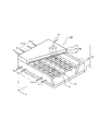
<画像表示装置>
図7は、マトリクス状に電子放出素子を配列した電子源を備えた画像表示装置の一例である。
<Image display device>
FIG. 7 shows an example of an image display apparatus provided with an electron source in which electron-emitting devices are arranged in a matrix.
X方向配線72が上述した第1の配線(4、5)に相当し、Y方向配線73が上述した第2の配線8に相当する。一対の電極12、13が、上述した第1の電極91と第2の電極92に相当する。また15は、上述した間隙11を備える導電性膜10に相当する。一対の電極12、13と間隙を備える導電性膜15とで、電子放出素子が構成される。
The
リアプレート71が上述した基板1に相当する。86はフェースプレートであり、ガラス基板83の表面には電子線が照射されることで発光する発光体層84(本発明の「発光体」に相当)と、アノード電極85とが設けられている。リアプレート71とフェースプレート86との間に支持枠82が設けられている。リアプレート71とフェースプレート86と支持枠82とで、内部が真空に保持された容器88が構成される。X方向配線72のそれぞれには端子(Dox1〜Doxm)が接続され、同様にY方向配線73のそれぞれには端子(Doy1〜Doym)が接続されている。アノード電極85には高圧電源と接続される端子87が接続されている。この容器と不図示の駆動回路とでフラットパネルディスプレイ101が構成される。
The
また、図7を用いて説明した本実施形態のがぞ外囲器(ディスプレイパネル)(88)を用いて画像再生装置を構成することができる。 Further, the image reproduction apparatus can be configured by using the envelope (display panel) (88) of the present embodiment described with reference to FIG.
具体的には、受信装置と、受信した信号を選曲するチューナーと、選曲した信号に含まれる信号を、ディスプレイパネル(88)に出力してスクリーンに表示または再生させる。上記受信装置は、テレビジョン放送などの放送信号又は無線回線網、電話回線網、ディジタル回線網、アナログ回線網、TCP/IPプロトコルで結ばれたインターネット等の電気通信回線を経由した信号を受信することができる。また、上記選曲した信号に含まれる信号としては、映像情報、文字情報および音声情報の少なくとも1つを指す。この構成によりテレビジョンなどの情報表示再生装置を構成することができる。勿論、放送信号がエンコードされている場合には、本発明の画像再生装置はデコーダーも含むことができる。また、音声信号については、別途設けたスピーカーなどの音声再生手段に出力して、ディスプレイパネル(88)に表示される映像情報や文字情報と同期させて再生する。 Specifically, the receiving device, the tuner for selecting the received signal, and the signal included in the selected signal are output to the display panel (88) to be displayed or reproduced on the screen. The receiving device receives a broadcast signal such as a television broadcast or a signal via a telecommunication line such as a wireless line network, a telephone line network, a digital line network, an analog line network, and the Internet connected by a TCP / IP protocol. be able to. The signal included in the selected signal indicates at least one of video information, character information, and audio information. With this configuration, an information display / playback apparatus such as a television can be configured. Of course, when the broadcast signal is encoded, the image reproducing apparatus of the present invention can also include a decoder. The audio signal is output to audio reproduction means such as a separately provided speaker and reproduced in synchronization with video information and character information displayed on the display panel (88).
また映像情報または文字情報をディスプレイパネル88に出力してスクリーンに表示および/あるいは再生させる方法としては、例えば以下のように行うことができる。まず、受信した映像情報や文字情報から、ディスプレイパネル88の各画素に対応した画像信号を生成する。そして生成した画像信号を、ディスプレイパネル88(図13のC11)の駆動回路(図13のC12)に入力する。そして、駆動回路に入力された画像信号に基づいて、駆動回路からディスプレイパネル88内の各電子放出素子に印加する電圧を制御して、画像を表示する。
As a method of outputting video information or character information to the
<テレビジョン装置>
図13は、画像再生装置の一例であるテレビジョン装置のブロック図である。受信回路(C20)は、チューナーやデコーダ等からなり、衛星放送や地上波等のテレビ信号や、無線回線網、電話回線網、ディジタル回線網、アナログ回線網、TCP/IPプロトコル
で結ばれたインターネット等の電気通信回を介したデータ放送等を受信し、復号化した映像データをI/F部(インターフェース部)(C30)に出力する。I/F部(C30)は、映像データを表示装置の表示フォーマットに変換して上記ディスプレイパネル(C11)に画像データを出力する。画像表示装置(C10)は、ディスプレイパネル(C11)、駆動回路(C12)及び制御回路(C13)を含む。制御回路は、入力した画像データに表示パネルに適した補正処理等の画像処理を施すともに、駆動回路(C12)に画像データ及び各種制御信号を出力する。駆動回路(C12)は、入力された画像データに基づいて、ディスプレイパネル(C11)の各配線7(図16のDox1〜Doxm、Doy1〜Doyn参照)に駆動信号を出力し、テレビ映像が表示される。受信回路(C20)とI/F部(C30)は、セットトップボックス(STB)として画像表示装置(C10)とは別の筐体に収められていてもよいし、また画像表示装置(C10)と同一の筐体に収められていてもよい。
<Television device>
FIG. 13 is a block diagram of a television device which is an example of an image reproducing device. The receiving circuit (C20) is composed of a tuner, a decoder, and the like, and is connected to a television signal such as satellite broadcast or terrestrial wave, a radio network, a telephone network, a digital network, an analog network, or the Internet via a TCP / IP protocol. The data broadcast etc. via the telecommunication times such as are received, and the decoded video data is output to the I / F unit (interface unit) (C30). The I / F unit (C30) converts the video data into the display format of the display device and outputs the image data to the display panel (C11). The image display device (C10) includes a display panel (C11), a drive circuit (C12), and a control circuit (C13). The control circuit performs image processing such as correction processing suitable for the display panel on the input image data, and outputs the image data and various control signals to the drive circuit (C12). Based on the input image data, the drive circuit (C12) outputs a drive signal to each wiring 7 (see Dox1 to Doxm, Doy1 to Doyn in FIG. 16) of the display panel (C11), and a television image is displayed. The The receiving circuit (C20) and the I / F unit (C30) may be housed in a separate housing from the image display device (C10) as a set top box (STB), or the image display device (C10). May be housed in the same housing.
また、インターフェースには、プリンター、デジタルビデオカメラ、デジタルカメラ、ハードディスクドライブ(HDD)、デジタルビデオディスク(DVD)などの画像記録装置や画像出力装置に接続することができる構成とすることもできる。そして、このようにすれば、画像記録装置に記録された画像をディスプレイパネル(C11)に表示させることもできる。また、ディスプレイパネル(C11)に表示させた画像を、必要に応じて加工し、画像出力装置に出力させることもできる画像再生装置(例えば、テレビジョン)を構成することができる。 Further, the interface can be configured to be connected to an image recording apparatus or an image output apparatus such as a printer, a digital video camera, a digital camera, a hard disk drive (HDD), or a digital video disk (DVD). And if it does in this way, the image recorded on the image recording device can also be displayed on a display panel (C11). In addition, it is possible to configure an image reproduction device (for example, a television) that can process an image displayed on the display panel (C11) as needed and output the image to an image output device.
ここで述べた画像再生装置の構成は、一例であり、本発明の技術思想に基づいて種々の変形が可能である。また、本発明の画像再生装置は、テレビ会議システムやコンピュータ等のシステムと接続することで、様々な画像再生装置を構成することができる。 The configuration of the image reproduction apparatus described here is an example, and various modifications can be made based on the technical idea of the present invention. In addition, the image reproduction apparatus of the present invention can be configured with various image reproduction apparatuses by connecting to a system such as a video conference system or a computer.
<実施例>
以下に本発明の実施例を示す。図9では、第1の配線4の片側に電子放出素子を設ける例で説明した。本実施例では、第1の配線4の両側に電子放出素子を設けた例を説明する。製造工程については図9を適宜参照する。尚、基板1をガラス基板1として、以下説明する。
<Example>
Examples of the present invention are shown below. In FIG. 9, the example in which the electron-emitting device is provided on one side of the
<実施例1>
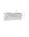
図1〜図5のマトリクスガラス基板を作製した。図1は、本実施例で作成した電子源ガラス基板の一部の平面模式図であり、図2は、図1のA−A線の断面模式図であり、図3は図1のB−B線の断面模式図である。
<Example 1>
The matrix glass substrate of FIGS. 1-5 was produced. FIG. 1 is a schematic plan view of a part of the electron source glass substrate prepared in this example, FIG. 2 is a schematic cross-sectional view taken along line AA in FIG. 1, and FIG. It is a cross-sectional schematic diagram of a B line.
始めに、ガラス基板1を用意する。ガラス基板1上にドライフィルムレジストを積層し、フォトグラフィー法により、溝2を形成部分のみのレジストを溶解し、保護膜を形成した。
First, a
次いで、サンドブラスト法を用いて溝幅を300ミクロン、溝深さを50ミクロンの溝2を形成した(図9(A))。
Next, a
次いで、ドライフィルムレジスト剥離し、次に、ガラス基板表面全域にSiO2膜を形成した。
次いで、白金製の一対の電極(91、92)を形成した(図9(B))。一対の電極(91、92)は、図1の符号9に相当する。
Next, the dry film resist was peeled off, and then an SiO 2 film was formed over the entire surface of the glass substrate.
Next, a pair of platinum electrodes (91, 92) was formed (FIG. 9B). The pair of electrodes (91, 92) corresponds to reference numeral 9 in FIG.
次に、撥油剤(アルキル系シランカップリング剤)を用いて、ガラス基板1の全面に形成した。この処理によりガラス基板11表面の接触角は、BCA(ブチルカルビトールア
セテート)に対し50度であった。
Next, it formed in the whole surface of the
次に、光透過部と光遮光部を備えたフォトマスクと、ガラス基板1との位置合わせを施し、低圧水銀灯(波長:254nm)を用い、紫外線を照射した。すなわち、溝2に相当する第1の領域(711)および第2の領域(712)に紫外線を照射し、基板1のその
他の領域である第3の領域(720)よりも親油性に変化させ(他の部分は撥油性のまま
)の撥油剤によりパターン3を形成した(図4、図9(C))。尚、第2領域(712)
には、電極(9)の一部が含まれている。
Next, alignment with the photomask provided with the light transmission part and the light-shielding part, and the
Includes a part of the electrode (9).
この結果、紫外線照射された領域(第1および第2の領域)に位置していた撥油剤が分解される。撥油剤が分解されることで形成された親油性領域(711、712)の接触角は、BCAに対し6度となり、撥油性領域(720)と親油性領域(711、712)との間には、40度以上の接触角の差を設けた(図4(A)、図4(B))。 As a result, the oil repellent agent located in the region (first and second regions) irradiated with ultraviolet rays is decomposed. The contact angle of the lipophilic region (711, 712) formed by decomposing the oil repellent is 6 degrees with respect to BCA, and between the oil repellent region (720) and the lipophilic region (711, 712). Provided a difference in contact angle of 40 degrees or more (FIGS. 4A and 4B).
次にスクリーン印刷法により導電性ペースト4(Agペースト(ガラスフリット成分を0.3wt%含有し、ブチルカルビトールアセテートを主溶媒とする))を、溝2内部へ落とし込むように印刷した。このときの充填量は、ガラス基板1の表面から、70ミクロン盛り上がるよう形成した。その後、常温下において20分放置し、導電性ペースト4を、充分に、第1の領域711上および第2の領域712上に行き渡らせた(図4(B))。
Next, conductive paste 4 (Ag paste (containing 0.3 wt% of glass frit component and butyl carbitol acetate as a main solvent)) was printed by screen printing so as to drop into the
導電性ペーストは、親油性が高い領域(711、712)で広がるため、電極9上まで延在するように導電性ペーストが流動する。親油性が低い領域(720)との境界まで導電性ペーストが到達するとその部分で導電性ペーストがせき止められ、電極9の一部を導電性ペーストが覆った。
Since the conductive paste spreads in the highly lipophilic region (711, 712), the conductive paste flows so as to extend onto the
次に、溶剤の乾燥を行った後、大気中で焼成を行い、電極9と接続された、ガラス基板表面とほぼフラットな第1の配線(4、5)(走査配線に相当する)を作製した(図5、図9(D))。大気中で焼成を行うことによりパターン3(撥油剤)は消失させることができる。
Next, after drying the solvent, firing is performed in the air, and the first wiring (4, 5) (corresponding to the scanning wiring) connected to the
次いで、感光性材料を混入した絶縁性ペーストをガラス基板1全面に形成し、フォトリソグラフィー法を用いて第1の配線(4、5)上に絶縁層7を形成した(図9(E))。
Next, an insulating paste mixed with a photosensitive material was formed on the entire surface of the
次に第1の配線(4、5)の形成に用いた導電性ペーストと同じ導電性ペーストを用いて第2の配線8(信号配線に相当する)を印刷法を用いて塗布し焼成することで形成し、マトリクス配線を備える配線基板を作製した(図9(F))。 Next, a second wiring 8 (corresponding to a signal wiring) is applied and baked by using the same conductive paste as the conductive paste used for forming the first wiring (4, 5) using a printing method. A wiring substrate provided with a matrix wiring was formed (FIG. 9F).
このとき、溝2の内壁と第1の配線との間で7ミクロンの隙間6は発生したものの、電
極9と配線(4、5)とは、良好な接続状態であった。
At this time, although a
次に、一対の電極9を接続するように、インクジェット法により、有機パラジウム含有溶液を塗布した後、加熱処理をして、酸化パラジウム(PdO)からなる導電性膜10を形成した(図9(G))。
Next, an organic palladium-containing solution was applied by an ink-jet method so as to connect the pair of
その後、第1の配線と第2の配線との間にパルス電圧を繰返し印加することで導電性膜10の一部に間隙11を形成した。続いて、炭素含有雰囲気中で第1の配線4と第2の配線8との間にパルス電圧を繰返し印加することで活性処理を行って、電子源を形成した(図9(H))。
Thereafter, a
本実施例で作成した電子源を駆動させたところ、長期に渡って、安定で、電子放出特性
のバラツキの少ない電子源を得ることができた。
When the electron source prepared in this example was driven, it was possible to obtain an electron source that was stable for a long time and had little variation in electron emission characteristics.
<実施例2>
溝2の形成、電極9の形成、及び撥油パターン形成は、実施例1と同様に行い、スクリーン印刷法により導電性ペースト(実施例1より、焼結時(焼成時)の収縮量の小さいAgペースト(ガラスフリット成分を1.0wt%))を溝2内部へ落とし込むように印刷した。
<Example 2>
The formation of the
溝2内への導電性ペーストの充填に際しては、Ag材料の焼結収縮を考慮して焼成後にガラス基板1の表面に対してほぼフラットになるよう、20ミクロン盛り上がるよう形成した。
When filling the
次に、溶剤の乾燥を行った後に、大気中で焼成を行い、ガラス基板1表面とほぼフラットな第1の配線(4、5)を作製した(図6)。これにより、溝の傍に位置するガラス基板1表面上に設けられた電極と溝内に設けられた配線との接続の信頼性を向上ができた。
Next, after drying the solvent, firing was performed in the air, and first wirings (4, 5) substantially flat with the surface of the
その後の工程は実施例1と同様に行い、マトリクス配線に接続された電子源を作製した。 Subsequent steps were performed in the same manner as in Example 1 to produce an electron source connected to the matrix wiring.
Ag材料の焼結収縮により、溝2の内壁と第1の配線との間で2ミクロンの隙間6が発
生したものの、電極9と第1の配線(4、5)とは、良好な接続状態であった。隙間6を
設けることでガラス基板1にクラックや割れを生じさせることを防止できる。
Although the sintering shrinkage of the Ag material produced a 2
そして、このように作成した電子源に対向するように蛍光体膜84とアルミからなるメタルバック85を備えるフェースプレート86を配置し、図7に示すディスプレイパネルからなる画像表示装置を形成した。そして、各信号配線(第2の配線8)と各走査配線(第1の配線4)に適宜所定の電圧を印加することで画像を表示させたところ、長期に渡って安定な画像を得ることができた。また、製造時および駆動時に発生する熱に対しても、走査配線がガラス基板1から剥がれることや、ガラス基板1の表面に微細なクラックが入ることもなく、各電子放出素子と配線との接続も安定であった。
Then, a face plate 86 having a phosphor film 84 and a metal back 85 made of aluminum was disposed so as to face the electron source thus created, and an image display device made up of a display panel shown in FIG. 7 was formed. When an image is displayed by appropriately applying a predetermined voltage to each signal wiring (second wiring 8) and each scanning wiring (first wiring 4), a stable image can be obtained over a long period of time. I was able to. In addition, the scanning wiring is not peeled off from the
以上説明したように、本実施例によれば、基板1の溝2に設けた第1の配線4と溝2の近傍に配置された電極9との接続が、安定的に形成できると共に、材料、プロセス面からローコストで、かつ、高精細なマトリクス配線構造を形成することが可能であり、極めて良好なフラットパネルディスプレイを簡易に形成することが可能である。
As described above, according to the present embodiment, the connection between the
1 基板
2 溝
4、5 第1の配線
7 絶縁層
8 第2の配線
DESCRIPTION OF
Claims (10)
けらており、前記第2の部分が前記溝に隣接する領域の一部の上に設けられている、配線基板の製造方法であって、
溝を備える基板を用意し、前記第2の部分が設けられる、前記溝に隣接する領域の一部の接触角と、当該一部を前記溝と囲む、前記溝に隣接する領域の他の一部の接触角とを異ならせた後に、少なくとも前記溝内および前記溝に隣接する領域の一部上に導電性ペーストを設ける、ことを特徴とする配線基板の製造方法。 (A) a substrate including a groove and a region adjacent to the groove; and (B) a first wiring including a first portion and a second portion extending from the first portion. The method of manufacturing a wiring board, wherein the first portion is provided in the groove, and the second portion is provided on a part of a region adjacent to the groove,
A substrate having a groove is prepared, and the second portion is provided. The contact angle of a part of the region adjacent to the groove and the other of the region adjacent to the groove surrounding the part with the groove. A method of manufacturing a wiring board, comprising: providing a conductive paste at least in the groove and on a part of a region adjacent to the groove after making the contact angle of the portion different.
けらており、前記第2の部分が前記溝に隣接する領域の一部の上に設けられている、配線基板の製造方法であって、
溝を備える基板を用意し、前記第2の部分が設けられる、前記溝に隣接する領域の一部の接触角と、当該一部を挟む、前記溝に隣接する領域の他の一部の接触角とを異ならせた後に、少なくとも前記溝内および前記溝に隣接する領域の一部上に導電性ペーストを設ける、ことを特徴とする配線基板の製造方法。 (A) a substrate including a groove and a region adjacent to the groove; and (B) a first wiring including a first portion and a second portion extending from the first portion. The method of manufacturing a wiring board, wherein the first portion is provided in the groove, and the second portion is provided on a part of a region adjacent to the groove,
A substrate having a groove is prepared, and a contact angle of a part of the area adjacent to the groove where the second part is provided, and a contact of another part of the area adjacent to the groove sandwiching the part. A method of manufacturing a wiring board, comprising: providing a conductive paste at least in the groove and on a part of a region adjacent to the groove after making the corners different.
前記導電性ペーストが前記電極の少なくとも一部を覆う
ことを特徴とする請求項1乃至3のいずれか1項に記載の配線基板の製造方法。 Before providing the conductive paste in the groove and on a part of the region adjacent to the groove, further comprising the step of providing an electrode in the region adjacent to the groove;
The method for manufacturing a wiring board according to claim 1, wherein the conductive paste covers at least a part of the electrode.
前記第1の配線と前記第2の配線との間に位置する絶縁層を設ける工程とを、更に、備えることを特徴とする請求項1乃至6のいずれか1項に記載の配線基板の製造方法。 Providing a second wiring that intersects the first wiring and is positioned on the first wiring;
The method for manufacturing a wiring board according to claim 1, further comprising a step of providing an insulating layer positioned between the first wiring and the second wiring. Method.
該配線基板上に配置され、前記第1の配線に接続する第1の電極と前記第2の配線に接続する第2の電極とを有する複数の電子放出素子と、
を備えた電子源の製造方法であって、
前記配線基板を請求項7に記載の配線基板の製造方法により製造することを特徴とする電子源の製造方法。 A wiring board provided with a first wiring and a second wiring on the board;
A plurality of electron-emitting devices disposed on the wiring substrate and having a first electrode connected to the first wiring and a second electrode connected to the second wiring;
A method of manufacturing an electron source comprising:
A method for manufacturing an electron source, wherein the wiring substrate is manufactured by the method for manufacturing a wiring substrate according to claim 7.
画像表示装置の製造方法であって、前記電子源が請求項8に記載の電子源の製造方法により製造されることを特徴とする画像表示装置の製造方法。 The manufacturing method of an image display apparatus provided with an electron source and the light-emitting body which light-emits by being irradiated with the electron discharge | released from this electron source, Comprising: The said electron source is a manufacturing method of the electron source of Claim 8 A method for manufacturing an image display device, wherein
Priority Applications (4)
| Application Number | Priority Date | Filing Date | Title |
|---|---|---|---|
| JP2006189282A JP2008016413A (en) | 2006-07-10 | 2006-07-10 | Manufacturing method of wiring board, manufacturing method of electron source, manufacturing method of image display device, and image reproduction device |
| US11/761,923 US7866039B2 (en) | 2006-07-10 | 2007-06-12 | Method for manufacturing wiring board for an image display |
| KR1020070064152A KR100906523B1 (en) | 2006-07-10 | 2007-06-28 | Manufacturing method of wiring board, manufacturing method of electron source, manufacturing method of image display apparatus and image reproducing apparatus |
| CNB2007101122788A CN100550252C (en) | 2006-07-10 | 2007-06-29 | The manufacture method of wiring plate, electron source and image display |
Applications Claiming Priority (1)
| Application Number | Priority Date | Filing Date | Title |
|---|---|---|---|
| JP2006189282A JP2008016413A (en) | 2006-07-10 | 2006-07-10 | Manufacturing method of wiring board, manufacturing method of electron source, manufacturing method of image display device, and image reproduction device |
Publications (2)
| Publication Number | Publication Date |
|---|---|
| JP2008016413A true JP2008016413A (en) | 2008-01-24 |
| JP2008016413A5 JP2008016413A5 (en) | 2009-08-20 |
Family
ID=38917887
Family Applications (1)
| Application Number | Title | Priority Date | Filing Date |
|---|---|---|---|
| JP2006189282A Withdrawn JP2008016413A (en) | 2006-07-10 | 2006-07-10 | Manufacturing method of wiring board, manufacturing method of electron source, manufacturing method of image display device, and image reproduction device |
Country Status (4)
| Country | Link |
|---|---|
| US (1) | US7866039B2 (en) |
| JP (1) | JP2008016413A (en) |
| KR (1) | KR100906523B1 (en) |
| CN (1) | CN100550252C (en) |
Families Citing this family (3)
| Publication number | Priority date | Publication date | Assignee | Title |
|---|---|---|---|---|
| JP2007335241A (en) * | 2006-06-15 | 2007-12-27 | Canon Inc | Wiring substrate, electron source, image display device and image reproducing device |
| JP4065551B2 (en) * | 2006-07-03 | 2008-03-26 | キヤノン株式会社 | Electron source, image display device, image reproducing device, wiring board, and method of manufacturing wiring board |
| DE102019201347B3 (en) | 2019-02-01 | 2020-06-18 | Lpkf Laser & Electronics Ag | Manufacture of metallic conductor tracks on glass |
Family Cites Families (21)
| Publication number | Priority date | Publication date | Assignee | Title |
|---|---|---|---|---|
| FR2325195A1 (en) * | 1975-09-18 | 1977-04-15 | Radiotechnique Compelec | ELECTROLUMINESCENT SEMICONDUCTOR MONOLITHIC ASSEMBLY |
| JP2737563B2 (en) * | 1992-08-18 | 1998-04-08 | 三菱電機株式会社 | Semiconductor light emitting device |
| JPH09265893A (en) * | 1996-03-29 | 1997-10-07 | Canon Inc | Electron emission element and electron source, image forming device, and manufacture of electron emission element |
| JP3530800B2 (en) * | 2000-05-08 | 2004-05-24 | キヤノン株式会社 | Electron source forming substrate, electron source using the substrate, and image display device |
| JP3548498B2 (en) * | 2000-05-08 | 2004-07-28 | キヤノン株式会社 | Electron source forming substrate, electron source using the substrate, and image display device |
| JP2001319564A (en) * | 2000-05-08 | 2001-11-16 | Canon Inc | Substrate for forming electron source, electron source and picture display device using this substrate |
| JP3703428B2 (en) * | 2000-12-18 | 2005-10-05 | キヤノン株式会社 | Electron source substrate and image forming apparatus manufacturing method |
| JP2002203475A (en) | 2001-01-04 | 2002-07-19 | Toshiba Corp | Electron source substrate, its manufacturing method and image display device provided with it |
| CN1215517C (en) * | 2001-08-02 | 2005-08-17 | 佳能株式会社 | Electron source and mfg. method thereof |
| US6653232B2 (en) * | 2001-08-03 | 2003-11-25 | Canon Kabushiki Kaisha | Method of manufacturing member pattern and method of manufacturing wiring, circuit substrate, electron source, and image-forming apparatus |
| US6866989B2 (en) * | 2001-09-07 | 2005-03-15 | Canon Kabushiki Kaisha | Method for forming patterned insulating elements and methods for making electron source and image display device |
| US6902455B2 (en) * | 2001-09-27 | 2005-06-07 | Canon Kabushiki Kaisha | Method of manufacturing member pattern, electron source, and image display device |
| US6903504B2 (en) * | 2002-01-29 | 2005-06-07 | Canon Kabushiki Kaisha | Electron source plate, image-forming apparatus using the same, and fabricating method thereof |
| JP2004146796A (en) * | 2002-09-30 | 2004-05-20 | Seiko Epson Corp | Method of forming film pattern, thin-film forming apparatus, electrically conductive film wiring, electrooptic device, electronic apparatus, and non-contact card medium |
| US7064475B2 (en) * | 2002-12-26 | 2006-06-20 | Canon Kabushiki Kaisha | Electron source structure covered with resistance film |
| JP4192737B2 (en) * | 2003-07-15 | 2008-12-10 | セイコーエプソン株式会社 | Layer pattern manufacturing method, wiring manufacturing method, electronic device manufacturing method |
| JP2005190769A (en) | 2003-12-25 | 2005-07-14 | Canon Inc | Electron source substrate, image display device using this, and manufacturing method of these |
| US7458872B2 (en) * | 2004-01-05 | 2008-12-02 | Canon Kabushiki Kaisha | Method of manufacturing electron-emitting device, electron source, and image display device |
| US7285428B2 (en) * | 2004-02-02 | 2007-10-23 | Canon Kabushiki Kaisha | Production method of electron source and image display |
| JP4065551B2 (en) * | 2006-07-03 | 2008-03-26 | キヤノン株式会社 | Electron source, image display device, image reproducing device, wiring board, and method of manufacturing wiring board |
| JP2008016226A (en) * | 2006-07-03 | 2008-01-24 | Canon Inc | Electron source, image display device, image reproduction device, wiring board, and manufacturing method of wiring board |
-
2006
- 2006-07-10 JP JP2006189282A patent/JP2008016413A/en not_active Withdrawn
-
2007
- 2007-06-12 US US11/761,923 patent/US7866039B2/en not_active Expired - Fee Related
- 2007-06-28 KR KR1020070064152A patent/KR100906523B1/en not_active IP Right Cessation
- 2007-06-29 CN CNB2007101122788A patent/CN100550252C/en not_active Expired - Fee Related
Also Published As
| Publication number | Publication date |
|---|---|
| US7866039B2 (en) | 2011-01-11 |
| US20080005899A1 (en) | 2008-01-10 |
| CN100550252C (en) | 2009-10-14 |
| KR100906523B1 (en) | 2009-07-07 |
| CN101106051A (en) | 2008-01-16 |
| KR20080005850A (en) | 2008-01-15 |
Similar Documents
| Publication | Publication Date | Title |
|---|---|---|
| US7679280B2 (en) | Substrate having a light emitter and image display device | |
| JP4920925B2 (en) | ELECTRON EMITTING ELEMENT, ELECTRON SOURCE USING SAME, IMAGE DISPLAY DEVICE, INFORMATION DISPLAY REPRODUCING DEVICE, AND ITS MANUFACTURING METHOD | |
| KR100479014B1 (en) | Display device and method of manufacturing the same | |
| KR20030078024A (en) | Cold cathode field emission device and process for the production thereof, and cold cathode field emission display and process for the production thereof | |
| JP2008027853A (en) | Electron emitting element, electron source, image display device, and method of manufacturing them | |
| JP2007294126A (en) | Electron emission element and manufacturing method thereof, electron source, and image display | |
| JP2008016413A (en) | Manufacturing method of wiring board, manufacturing method of electron source, manufacturing method of image display device, and image reproduction device | |
| JP2008030992A (en) | Method for manufacturing substrate, method for manufacturing wiring substrate, wiring substrate, electronic device, electron source, and image display | |
| JP2007335241A (en) | Wiring substrate, electron source, image display device and image reproducing device | |
| JP2008016226A (en) | Electron source, image display device, image reproduction device, wiring board, and manufacturing method of wiring board | |
| JP2002245927A (en) | Substrate with thin lines, electronic source, and image display device | |
| JP4065551B2 (en) | Electron source, image display device, image reproducing device, wiring board, and method of manufacturing wiring board | |
| JP2009277458A (en) | Electron emitter and image display apparatus | |
| JP2004165152A (en) | Manufacturing method of airtight container, manufacturing method of image display device, and bonding method | |
| JP4366054B2 (en) | Matrix wiring manufacturing method, electron source, and image forming apparatus manufacturing method | |
| JP2006073247A (en) | Image display device | |
| KR101022656B1 (en) | Electron emission display and the fabrication method thereof | |
| JP2009037792A (en) | Image display device | |
| JP2009289717A (en) | Method for manufacturing plasma display panel | |
| JP2005353453A (en) | Image display device | |
| JP2009043437A (en) | Image display device and its manufacturing method | |
| JP2010067477A (en) | Electron emitting device, electron source, visual display unit, information display reproducing apparatus, and method for manufacturing them | |
| JP2006012700A (en) | Manufacturing method of electron emitting element and display device | |
| JP2006107776A (en) | Manufacturing method of image display device | |
| JP2003297225A (en) | Electron source substrate and its manufacturing method, as well as image forming device |
Legal Events
| Date | Code | Title | Description |
|---|---|---|---|
| A521 | Request for written amendment filed |
Free format text: JAPANESE INTERMEDIATE CODE: A523 Effective date: 20090706 |
|
| A621 | Written request for application examination |
Free format text: JAPANESE INTERMEDIATE CODE: A621 Effective date: 20090706 |
|
| A761 | Written withdrawal of application |
Free format text: JAPANESE INTERMEDIATE CODE: A761 Effective date: 20110610 |