JP2007294126A - Electron emission element and manufacturing method thereof, electron source, and image display - Google Patents
Electron emission element and manufacturing method thereof, electron source, and image display Download PDFInfo
- Publication number
- JP2007294126A JP2007294126A JP2006117730A JP2006117730A JP2007294126A JP 2007294126 A JP2007294126 A JP 2007294126A JP 2006117730 A JP2006117730 A JP 2006117730A JP 2006117730 A JP2006117730 A JP 2006117730A JP 2007294126 A JP2007294126 A JP 2007294126A
- Authority
- JP
- Japan
- Prior art keywords
- electron
- region
- film
- electron emission
- emitting device
- Prior art date
- Legal status (The legal status is an assumption and is not a legal conclusion. Google has not performed a legal analysis and makes no representation as to the accuracy of the status listed.)
- Withdrawn
Links
Images


Classifications
-
- H—ELECTRICITY
- H01—ELECTRIC ELEMENTS
- H01J—ELECTRIC DISCHARGE TUBES OR DISCHARGE LAMPS
- H01J1/00—Details of electrodes, of magnetic control means, of screens, or of the mounting or spacing thereof, common to two or more basic types of discharge tubes or lamps
- H01J1/02—Main electrodes
- H01J1/30—Cold cathodes, e.g. field-emissive cathode
- H01J1/304—Field-emissive cathodes
-
- H—ELECTRICITY
- H01—ELECTRIC ELEMENTS
- H01J—ELECTRIC DISCHARGE TUBES OR DISCHARGE LAMPS
- H01J31/00—Cathode ray tubes; Electron beam tubes
- H01J31/08—Cathode ray tubes; Electron beam tubes having a screen on or from which an image or pattern is formed, picked up, converted, or stored
- H01J31/10—Image or pattern display tubes, i.e. having electrical input and optical output; Flying-spot tubes for scanning purposes
- H01J31/12—Image or pattern display tubes, i.e. having electrical input and optical output; Flying-spot tubes for scanning purposes with luminescent screen
- H01J31/123—Flat display tubes
- H01J31/125—Flat display tubes provided with control means permitting the electron beam to reach selected parts of the screen, e.g. digital selection
- H01J31/127—Flat display tubes provided with control means permitting the electron beam to reach selected parts of the screen, e.g. digital selection using large area or array sources, i.e. essentially a source for each pixel group
-
- H—ELECTRICITY
- H01—ELECTRIC ELEMENTS
- H01J—ELECTRIC DISCHARGE TUBES OR DISCHARGE LAMPS
- H01J9/00—Apparatus or processes specially adapted for the manufacture, installation, removal, maintenance of electric discharge tubes, discharge lamps, or parts thereof; Recovery of material from discharge tubes or lamps
- H01J9/02—Manufacture of electrodes or electrode systems
- H01J9/022—Manufacture of electrodes or electrode systems of cold cathodes
- H01J9/025—Manufacture of electrodes or electrode systems of cold cathodes of field emission cathodes
Abstract
Description
電子放出素子、該電子放出素子を複数配置してなる電子源、該電子源を用いて構成した画像表示装置に関する。 The present invention relates to an electron-emitting device, an electron source in which a plurality of electron-emitting devices are arranged, and an image display device configured using the electron source.
電子放出素子には、電界放出型(以下、「FE型」と称する)の電子放出素子や、表面伝導型の電子放出素子がある。 The electron-emitting device includes a field emission type (hereinafter referred to as “FE type”) electron emission device and a surface conduction type electron emission device.
FE型の電子放出素子には、電子ビームの広がりが少ない電子放出素子の例として、特許文献1〜3のように、平坦な電子放出膜上に、開口(いわゆる「ゲートホール」)を備える、ゲート電極を備えた電子放出素子がある。このような平坦な電子放出膜を有する電子放出素子では、電子放出膜表面に比較的平坦な等電位面が形成されるため、電子ビームの広がりを小さくすることができる。
The FE type electron-emitting device includes an opening (so-called “gate hole”) on a flat electron-emitting film as an example of an electron-emitting device with a small electron beam spread, as in
一方で電子放出素子を用いた画像表示装置では、輝度均一性などの信頼性を確保するために安定した電子放出を行わなければならない。具体的には、電子放出素子が駆動中に過電流などによって破壊されるのを防止しなければならない。さらに電子放出量が経時的に変動することを防ぐ、つまり電子放出量のをゆらぎを小さくしなければならない。この対策として特許文献4では、電極を複数に分割した電子放出素子が開示されている。また、特許文献5では、多孔質アルミナの微小空間に抵抗材料を充填し、さらに、微粒子などの電子放出材料を固着材料を用いて充填した電子放出素子が開示されている。
上記した平坦な電子放出膜を有する電子放出素子(FE型の電子放出素子)を作製する場合、電子放出膜上に、連通する開口を有する絶縁層及びゲート電極を設ける必要がある。そして、このような電子放出素子は基体上に配置される。 When an electron-emitting device having the above flat electron-emitting film (FE type electron-emitting device) is manufactured, it is necessary to provide an insulating layer having a communicating opening and a gate electrode on the electron-emitting film. And such an electron-emitting device is arrange | positioned on a base | substrate.
しかし、電子放出素子を構成する部材のそれぞれの材料、厚さによっては、高い応力が発生する場合があり、さらには、基体から電子放出素子が剥離したり、電子放出膜が剥離してしまう場合もある。この傾向は、特に、電子放出特性の良好な、ダイヤモンドライクカーボンを主体とする膜やアモルファスカーボンを主体とする膜に代表される炭素を主成分とする膜を電子放出膜に用いた場合に顕著である。 However, depending on the material and thickness of each member constituting the electron-emitting device, high stress may be generated, and further, the electron-emitting device may be peeled off from the substrate or the electron-emitting film may be peeled off. There is also. This tendency is particularly noticeable when a film mainly composed of diamond-like carbon or a film mainly composed of amorphous carbon, which has good electron emission characteristics, is used as the electron emission film. It is.
また、平坦な電子放出膜を有する電子放出素子では、電子放出量のゆらぎを小さくするために電流制限用の抵抗層を積層すると、上記したような理由から電子放出膜が基体から剥離してしまう場合がある。 In addition, in an electron-emitting device having a flat electron-emitting film, if a current-limiting resistance layer is stacked in order to reduce fluctuations in the amount of electron emission, the electron-emitting film is peeled off from the substrate for the reasons described above. There is a case.
また、特許文献1に開示されたような金属を含む電子放出膜では、その電子放出膜中の金属量を制御することが重要である。しかし、電子放出膜中の金属が、電子放出膜に接する電極(例えば)カソード電極などに移動してしまうと、電子放出膜中の金属量などが変化し、電子放出特性が変化する場合がある。従って、電子放出膜中の金属が、電子放出膜に接するカソード電極などの部材に移動するのを防止するための層を設ける必要がある。そして、一方で、前述した様に電子放出膜が剥離しないようにする必要がある。
Moreover, in the electron emission film containing a metal as disclosed in
そこで、本発明は、電子放出量のゆらぎが小さく、かつ電子放出膜が基体や電子放出膜が接する部材(例えばカソード電極)から剥離することが抑制され、そして、電子放出特性の変動の小さい電子放出素子およびその製造方法を提供することを目的とする。 Therefore, the present invention is an electron in which fluctuation of the electron emission amount is small, separation of the electron emission film from a substrate or a member (for example, a cathode electrode) in contact with the electron emission film is suppressed, and an electron emission characteristic fluctuation is small. It is an object of the present invention to provide an emission element and a method for manufacturing the same.
上記目的を達成するために成された本発明は、以下の通りである。 The present invention made to achieve the above object is as follows.
即ち、本発明は、導電層と該導電層上に配置された電子放出膜とを備える電子放出素子であって、前記導電層が、複数の第1領域と、複数の第1領域の各々の間に設けられた、前記第1領域よりも高抵抗な第2領域とを、少なくとも有する表面を備えており、前記電子放出膜が、前記導電層の前記表面を覆っている、ことを特徴とする。 That is, the present invention is an electron-emitting device including a conductive layer and an electron-emitting film disposed on the conductive layer, wherein the conductive layer includes a plurality of first regions and a plurality of first regions. A surface having at least a second region having a resistance higher than that of the first region, and the electron emission film covers the surface of the conductive layer. To do.
また、本発明は、(A)基体と、(B)各々が前記基体の表面に対して実質的に垂直に配向した、複数の柱状の第1領域と、(C)前記複数の第1領域の各々の間に設けられた、前記第1領域よりも高抵抗な第2領域と、(D)前記複数の柱状の第1領域と前記第2領域とを覆う電子放出膜と、を備えることを特徴とする。 The present invention also includes (A) a base, (B) a plurality of columnar first regions each oriented substantially perpendicular to the surface of the base, and (C) the plurality of first regions. A second region having a higher resistance than the first region, and (D) an electron emission film covering the plurality of columnar first regions and the second region. It is characterized by.
また、本発明は、導電層と該導電層上に配置された電子放出膜とを備える電子放出素子の製造方法であって、(i)(a)導電性の複数の柱状領域を具備する導電層と、(b)該導電層上に配置された、金属を含有する層と、を備える構造体を用意する工程、(ii)前記構造体を加熱する工程、とを有することを特徴とする。 The present invention also relates to a method for manufacturing an electron-emitting device including a conductive layer and an electron-emitting film disposed on the conductive layer, wherein (i) (a) a conductive material having a plurality of conductive columnar regions. And (b) a step of preparing a structure including a metal-containing layer disposed on the conductive layer, and (ii) a step of heating the structure. .
本発明によれば、電子放出素子の基体からの剥離を防止し、カソード電極とは別に電流を制限するための抵抗層を設ける必要なく、電子放出量のゆらぎの小さい電子放出素子およびその製造方法を提供することができる。 According to the present invention, there is no need to provide a resistance layer for limiting the current separately from the cathode electrode, preventing the peeling of the electron-emitting device from the substrate, and an electron-emitting device having a small fluctuation in the amount of electron emission and a method for manufacturing the same Can be provided.
以下、図面を用いて、本発明の好適な実施形態を例示的に詳しく説明する。但し、下記の実施形態に記載されている構成部品の寸法、材質、形状、その相対位置などは、特に記載のない限りは、この発明の範囲をそれらに限定する趣旨のものではない。 DESCRIPTION OF EXEMPLARY EMBODIMENTS Hereinafter, exemplary embodiments of the invention will be described in detail with reference to the drawings. However, the dimensions, materials, shapes, relative positions, and the like of the components described in the following embodiments are not intended to limit the scope of the present invention unless otherwise specified.
図1は本発明の電子放出素子の一例の断面模式図である。本発明の電子放出素子は、基体1の表面上に配置されており、導電層2と、導電層2上に位置する電子放出膜5と、を少なくとも備える。尚、導電層2を、「カソード電極」あるいは「電極」と呼ぶ場合もある。
FIG. 1 is a schematic cross-sectional view of an example of the electron-emitting device of the present invention. The electron-emitting device of the present invention is disposed on the surface of the
また、導電層2は、導電性の複数の第1領域3と、隣り合う第1領域3の間に設けられ、第1領域3よりも低い導電性を備えた領域4と、を少なくとも含む。導電層2はその表面に、上記複数の第1領域3の端部および第2領域4の端部を備えている。そして、導電層2の表面上に電子放出膜5が載置されているので、上記複数の第1領域3の端部と電子放出膜5とが電気的に接続された形態であると言う事ができる。尚、導電層2と電子放出膜5との間に何らかの層が配置された形態であっても、本発明の効果を奏する範囲内であれば、そのような形態も本発明の範囲内である。つまり、導電層2の表面に例えば薄い酸化膜が形成されていても、第1領域3の各々から電子放出膜5に電子が供給される状態であれば本発明の効果を奏する範囲内と言うことが出来る。また、複数の第1の領域3の各々は、領域4によって実質的に互いに電気的に分離された、「導電性のセル」または「導電性のチャネル」または「電流経路」と言い換える事も出来る。
In addition, the
図1では、各第1の領域3から電子放出膜5への電流供給をより効率良く行うために、導電層2が更に、第3の領域101を備えた形態の電子放出素子を示した。この形態では、第1の領域3の導電率以上の導電率を備える材料で第3の領域101が構成される(第3の領域101が第1の領域3以上に低抵抗である)ことが好ましい。そして、この形態では、第3の領域101上に、複数の第1の領域3が載置されることになる。従って、第1の領域3の各々は、第3の領域101を介して電気的に共通に接続された形態と言う事が出来る。そして、この様な形態では、第3の領域101は膜状に形成されることが好ましいため、第3の領域は、導電性膜と言い換えることもできる。この様な形態の場合は、第1の領域3と第2の領域4とが、電子放出膜5と第3の領域101とに挟まれた形態と言う事ができる。尚、第3の領域101は典型的には金属膜で構成することができる。
FIG. 1 shows an electron-emitting device in which the
また、本発明の電子放出素子は、図1で示した第3の領域101と第1の領域3との間に、さらに、抵抗体を加えた形態であっても良い。この形態では、第3の領域101と各第1の領域3との間に、抵抗体としての第4の領域(不図示)が配置される。この第4の領域は、第3の領域と同様、膜状に形成されることが好ましい。そのため、第4の領域は、抵抗膜と呼ぶこともできる。そして、各第1の領域3は、第4の領域を介して共通に接続された形態となる。この様な形態の場合は、複数の第1の領域3と第2の領域4とが、電子放出膜5と第4の領域とに挟まれた形態ということができる。また、抵抗層としての第4の領域を用いる場合には、その抵抗値にもよるが、上述した第3の領域101を必要としない場合もある。
In addition, the electron-emitting device of the present invention may have a configuration in which a resistor is further added between the
このように、第1の領域3と基体1との間に第3の領域101が配置される場合には、電子放出素子を駆動するための電源は、第3の領域101に接続される。尚、第4の領域が第3の領域101と共に用いられる場合においては、電子放出素子を駆動するための電源は、第3の領域101に接続される。しかしながら、第3の領域101を用いずに、第1の領域3と基体1との間に第4の領域が配置される場合には、電子放出素子を駆動するための電源は、第4の領域101に接続されることが好ましい。
As described above, when the
尚、本発明の電子放出素子は、図10に示す様に、上述した第3の領域101(及び/または第4の領域)を備えない形態であっても良い。この様な形態の場合は、複数の第1の領域3と第2の領域4とが、電子放出膜5と基体1とに挟まれた形態と言う事ができる。
As shown in FIG. 10, the electron-emitting device of the present invention may have a form not including the third region 101 (and / or the fourth region) described above. In the case of such a form, it can be said that a plurality of
ここでは、第1の領域3を柱状の領域で構成した形態を示したが、第1の領域3は柱状に限られるものではなく、例えば球状など別の形状であっても良い。しかしながら、電子放出点数を高密度に設け、電子放出量のゆらぎを低減するため、並びに、電子放出膜5と導電層2との密着性を確保するためには、第1の領域3は柱状であることが好ましい。
Here, although the form which comprised the 1st area |
第1の領域3が柱状の場合は、導電層2は、複数の柱状の第1の領域3と、領域3よりも低い導電性を備えた領域4と、を少なくとも含む。そのため、このような複数の柱状の第1の領域3と、第1の領域3よりも低い導電性を備えた第2の領域4と、を有する構造体100を、「柱状構造」または「柱状結晶」と呼ぶこともできる。
When the
ここで、図1に示した複数の柱状領域3の各々は、基体1が備える表面(平面)に対して垂直な方向に配向している。本発明における柱状領域3は、図1に示した様に基体1の表面(第3の領域101の表面)に対して垂直に、その長手方向が揃えられた形態だけでなく、図10に示す様に、その長手方向が基体1の表面に対して実質的に垂直な方向に設定された形態であっても良い。その場合、柱状領域3の輪郭線(あるいは柱状領域3の中心線)と、基体表面に対する垂線とのなす角θは、0°に近いほど好ましいが、電子放出特性の均一性の観点から、実用的な範囲としては、0°以上30°以下の範囲に設定すればよい。
Here, each of the plurality of
また、図1に記載の電子放出素子の形態は、多数の柱状領域3の各々の長手方向が、実質的に一方向に揃っており(上記実用的な範囲内であり)、多数の柱状領域3の各々の長手方向における一方の端部を電子放出膜5が覆っている形態と言うこともできる。あるいはまた、多数の柱状領域3の各々は、その長手方向において2つの対向する端部を備えており、その長手方向が基体1の表面に対して実質的に垂直な方向に配置されている形態と言うこともできる。尚、上記長手方向は、柱状領域3の輪郭線あるいは柱状領域3の中心線が延在する方向と言い換えることもできる。
Further, in the configuration of the electron-emitting device shown in FIG. 1, the longitudinal direction of each of the multiple
尚、第1の領域3が柱状であり、さらに上述した第3の領域を備える形態では、電子放出膜5と第3の領域101とが対向する方向と、各柱状領域3の長手方向とが、実質的に平行であると言う事ができる。また、特に、第3の領域101が導電性膜であれば、各柱状領域3が、電子放出膜5および第3の領域101である導電性膜に対して実質的に垂直に配向された形態と言うことが出来る。
In the embodiment in which the
柱状領域3は、図1中に示す、高さ(厚み)dと、柱状領域3の直径(基体1の表面に平行な方向における「長さ」または「幅」)Wにより規定することができる。各々の柱状領域3を基体1の表面に平行な面で切った時の断面形状(平面形状)は、電子放出領域の密度を高くする観点から、円形であることが好ましいが、三角形や四角形や五角形などの多角形状であっても良い。
The
長さW’は、領域3(第1の領域3)が周期的に配列した場合では、1周期長(ピッチ)に相当する。W’−Wは、第2の領域4の長さと言う事もできる。あるいは、W’−Wは、2つの隣合う第1領域3間の最短距離と言い換えることができる。
The length W ′ corresponds to one cycle length (pitch) when the regions 3 (first regions 3) are periodically arranged. W′-W can also be said to be the length of the second region 4. Alternatively, W′-W can be rephrased as the shortest distance between two adjacent
ここでは、第1の領域3を柱状の領域で構成した形態を示したが、第1の領域3は柱状ではなく球状など別の形状であっても良い。いずれにしても、本発明において、複数の第1の領域3の各々は、領域4によって実質的に互いに電気的に分離された、「導電性のセル」または「電流経路」と考えることができる。
Here, although the form which comprised the 1st area |
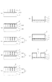
本発明の電子放出素子は、図2(a)、(b)に模式的に示す形態であっても良い。図2(a)は平面図であり、図2(b)は、図2(a)のb−b’における断面図である。即ち、図1に示した電子放出膜5の上に、開口を備えた絶縁層7と開口を備えた第2の電極8とを備える形態である。絶縁層5と第2の電極8には連通する(貫通する)開口21が設けられている。この形態の電子放出素子では、導電層2の電位よりも高い電位を第2の電極8に印加することで、電子放出膜5から電子を放出する。従って、第2の電極8が、電子放出膜5から電子を電界放出させるために必要な電界を生成する。そのため、第2の電極8が、いわゆる「引出し電極」または「ゲート電極」に相当する。開口21は、ここでは円形の例を示したが、矩形や多角形状であっても構わない。
The electron-emitting device of the present invention may have a form schematically shown in FIGS. 2 (a) and 2 (b). FIG. 2A is a plan view, and FIG. 2B is a cross-sectional view taken along line b-b ′ in FIG. In other words, on the
また、本発明の電子放出素子は、図7(a)〜(c)に模式的に示す形態であっても良い。図7(a)は平面図であり、図7(b)は、図7(a)のb−b’における断面図である。また、図7(c)は、図7(a)のb−b’における断面における変形例である。 Further, the electron-emitting device of the present invention may have a form schematically shown in FIGS. FIG. 7A is a plan view, and FIG. 7B is a cross-sectional view taken along line b-b ′ in FIG. FIG. 7C is a modification of the cross section taken along the line b-b ′ in FIG.
図2で示した形態では、1つの電子放出素子に、1つの開口21を備えた形態を示した。しかしながら、本発明の電子放出素子では、図7(a)に示す様に、1つの電子放出素子に、複数の開口21を備える形態であっても良い。そして、図7(c)は、電子放出膜5が開口21内のみに配置された形態である。尚、図7と図2では、同じ部材には同じ符号を用いている。
In the form shown in FIG. 2, a form in which one
本発明の電子放出素子を用いた電子放出装置(画像表示装置も含む)では、例えば図9に示すように、一般にはトライオード構造(導電層2、第2の電極8、アノード9)を採用する。勿論、電極8を用いずに、図1に示した電子放出素子に対向する様に、アノード9を配置してダイオード構造の電子放出装置を構成する事も可能である。
In an electron emission device (including an image display device) using the electron emission element of the present invention, a triode structure (
図9では、図2に示した形態の本発明の電子放出素子が配置された基体1の表面と実質的に平行になるように、第3電極であるところのアノード電極9を配置している。アノード電極9には、電子放出膜5と第2の電極8の電位よりも高い電位が印加される。駆動時には、第2の電極8に、電子放出膜5の電位よりも高い電位を印加することで、電子放出膜5から電子が放出される。典型的には、第2の電極8に第3の領域101の電位よりも高い電位が印加され、そして、第2の電極8の電位よりも十分に高い電位がアノード9に印加される。放出された電子は、開口21を通り抜けた後、アノード電極9の電位によってアノード9に引き寄せられ、アノード電極9に衝突する。
In FIG. 9, the anode electrode 9 serving as the third electrode is arranged so as to be substantially parallel to the surface of the
導電層2が図1のような柱状構造を採用した場合、導電層2全体の応力を好ましく緩和することができ、基体1から電子放出膜5が剥離し難くすることができる。
When the
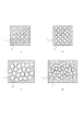
導電層2を、基体1表面の上方から見た様子の一例を、図11(a)〜(d)に示す。図11(a)〜(c)では領域3の平面(断面)形状が円形の場合を示し、図11(d)では、領域3の平面(断面)形状が多角形の一例である三角形の場合を示している。また、複数の領域3の各々の平面(断面)形状は、同じものあるいは実質的に同じものが並んでいてもよいし、様々な形態のものが混在していても構わない。
An example of the state of the
また、複数の領域3の配列形態は様々な形態を採用することができる。例えば、図11(b)に示すように、領域3の密度が高くなるように、多数の領域3が蜂の巣状に並んだ形態であっても良いし、図11(a)に示す様に、行列状に配置された形態であっても良い。あるいは、図11(a)や図11(b)の形態に比べて秩序性が低い(ランダムな)、図11(c)や(d)に示すような形態であっても良い。
In addition, various forms can be adopted as the arrangement form of the plurality of
また、本発明では、全ての領域3が完全に領域4によって分離されている形態が好ましい。しかしながら、本発明の効果を奏する限り、わずかな数の領域3同士が、領域4を実効的に間に挟まずに、互いに接しているような形態であっても構わない。
In the present invention, it is preferable that all the
領域3の直径Wは、領域3を上方から見た際の(領域3の平面形状における)、最小外接円の直径で定義することができる。換言すると、各々の領域3の直径Wは、導電層2の表面に存在する(露出する)領域3の最小外接円の直径で定義することができる。
The diameter W of the
第1の領域3を構成する材料は、導電性材料であればよく、金属や導電性の金属化合物が好ましい。例えば、Be、Mg、Ti、Zr、Hf、V、Nb、Ta、Mo、W、Al、Cu、Ni、Cr、Au、Pt、Pd等の金属、またはこれらの金属を含む合金を用いることができる。特に好ましくは、耐熱性が良好な材料である、Ti、TiN、Ta、TaN、AlN、TiAlNが用いられる。
The material which comprises the 1st area |
領域3の高さ(厚み)dは、実用的には、10nm以上10μm以下の範囲で選択され、好ましくは10nm以上1μm以下の範囲で選択される。領域3の直径Wは、実用的には、1nm以上100nm以下の範囲で選択され、好ましくは1nm以上10nm以下の範囲で選択される。上述した領域3の高さdは、領域3が柱状である場合は、柱状領域3の長手方向における長さと言い換えることもできる。あるいは、柱状領域3の長手方向における2つの端部の間の距離と言い換えることもできる。尚、ここで言う2つの端部は、一方が電子放出膜5に接する端部であり、もう一方が基体1(あるいは第3の領域101)に接する端部である。
The height (thickness) d of the
隣り合う2つの領域3の間に配置される領域4は、領域3よりも低い導電性を備えている。
The region 4 disposed between the two
また、本発明の効果をより大きくする上では、第2の領域4の比抵抗(抵抗率)ρ4と第1の領域3の比抵抗(抵抗率)ρ3との比(ρ4/ρ3)は大きいほど好ましい。ρ4/ρ3の実用的な範囲としては、少なくとも104以上、好ましくは106以上、更に好ましくは108以上である。 Further, in order to increase the effect of the present invention, the ratio of the first resistivity (resistivity) of the second region 4 [rho 4 and the specific resistance (resistivity) of the first region 3 ρ 3 (ρ 4 / ρ 3 ) is preferably as large as possible. The practical range of ρ 4 / ρ 3 is at least 10 4 or more, preferably 10 6 or more, and more preferably 10 8 or more.
そして、電流制限効果を得るために、実用的には、領域4の比抵抗ρ4は108Ω・cm以上であることが好ましく、実用的には108Ω・cm以上1012Ω・cm以下であることがより好ましい。一方、領域3の抵抗率ρ3は10‐6Ω・cm以上であることが好ましく、実用的には10‐6Ω・cm以上104Ω・cm以下であることがより好ましい。本発明において、108Ω・cm以上である領域4は絶縁体と言い換えることもできる。 In order to obtain a current limiting effect, practically, the specific resistance ρ 4 of the region 4 is preferably 10 8 Ω · cm or more, and practically, 10 8 Ω · cm or more and 10 12 Ω · cm. The following is more preferable. On the other hand, it is preferable that the resistivity [rho 3 region 3 is 10 -6 Ω · cm or more, and more preferably practically not more than 10 -6 Ω · cm or more 10 4 Ω · cm. In the present invention, the region 4 that is 10 8 Ω · cm or more can also be referred to as an insulator.
領域4を構成する材料としては、酸化物、窒化物、酸窒化物(酸化物と窒化物の混合物も含む)を用いることができる。より具体的には、酸化チタン、酸化チタンと窒化チタンの混合物、酸化シリコン(典型的にはシリカ)、窒化シリコン、アルミナなどの絶縁体であればよい。また、酸化物であることがより好ましい。酸化物としては、金属の酸化物または半導体の酸化物を好ましく用いることができる。そして、特には、領域3を構成する材料の酸化物であることが、特に簡易で好ましい。さらに好ましくは、領域3の表面を酸化することで、領域4を構成する。
As a material constituting the region 4, an oxide, a nitride, or an oxynitride (including a mixture of an oxide and a nitride) can be used. More specifically, an insulator such as titanium oxide, a mixture of titanium oxide and titanium nitride, silicon oxide (typically silica), silicon nitride, or alumina may be used. Moreover, it is more preferable that it is an oxide. As the oxide, a metal oxide or a semiconductor oxide can be preferably used. In particular, an oxide of the material constituting the
尚、領域3を窒化チタンで構成し、その表面を酸化することで領域4を形成した場合は、領域4は、少なくとも酸化チタンを含んでおり、場合によってはさらに窒化チタンを含む。後述する例えば実施例1に記載の製造方法を用いれば、簡易に、柱状の領域3を形成できる。但し、電子放出素子の駆動時における熱的な安定性などを考慮すると、領域4は、酸化チタンと窒化チタンの混合物で構成されていることが好ましい。
When the
領域4を、隣合う領域3同士の間に配置することで、導電層2は、実質的に、領域3の数に分割される(領域3の直径サイズに分割される)。そのため、導電層2の膜厚方向(導電層2と電子放出膜3とが積層される方向)への導電経路が、領域3のサイズWに制限することができる。つまり、カソード導電層2を通り電子放出膜5に到達する電流量を制限することができるので、別途、電流を制限するための抵抗層を設けなくとも、電子放出膜5からの電子放出量のゆらぎを小さくすることができる。
By disposing the region 4 between the
尚、領域3の抵抗率ρ3及び領域4の抵抗率ρ4を実測する手法は特に限定されるものではなく様々な手法を用いることができる。例えば、まず、金属膜上に、本発明の導電層2を配置する。そして、走査型トンネル顕微鏡(STM)のプローブで領域3(領域4)を走査しながら金属膜とプローブとの間に電圧を印加する。これにより領域3(領域4)を流れる電流を測定し、ρ3(ρ4)を測る方法を用いる事が出来る。
The method for actually measuring the resistivity ρ 3 in the region 3 and the resistivity ρ 4 in the region 4 is not particularly limited, and various methods can be used. For example, first, the
本発明の電子放出膜5は、電子放出特性の良好性および安定性から、炭素を主体(母材または主成分)として構成されることが好ましい。特には、好ましくは、電子放出膜5の主体は、ダイヤモンド、ダイヤモンドライクカーボン(DLC)、アモルファスカーボンから選択される。ただし、電子放出膜5の主体の抵抗率は高く、実質的に、絶縁体として機能することが好ましい。そのため、電子放出膜3の主体としては、ダイヤモンドライクカーボンやアモルファスカーボンを用いることが好ましい。実用的には、電子放出膜5の主体は、1×10⁸以上1×10¹⁴Ω・cm以下の抵抗率を備えることが好ましい。また、詳しくは後述するが、本発明の電子放出膜5は金属を含む形態であってもよい。尚、電子放出膜3全体の抵抗率については100Ω・cm以上1010Ω・cm以下であることが好ましい。
The
そして、電子放出膜5は、金属膜などのような良導体の膜ではないことが求められる。この理由は、電子放出膜5が良導体の場合、各導電経路(各領域3)内に移動範囲が制限された電子が、電子放出膜5中で広がってしまい、放出電流のゆらぎが多くなってしまう為である。
The
一方で、電子放出膜5の比抵抗(実質的に電子放出膜5の主体の比抵抗と言い換えることができる)ρ5が大きい場合には、電子放出膜5の膜厚(柱状領域3の長手方向における厚み)d’を考慮する必要がある。これは、高抵抗な電子放出膜5の膜厚d’が大きいと、電子放出膜5の表面または表面近傍に存在すると想定される電子放出部から十分な量の電子を低い駆動電圧で放出させることが困難になるためである。
On the other hand, when the specific resistance ρ 5 of the electron emission film 5 (substantially the specific resistance of the main body of the electron emission film 5) ρ5 is large, the film thickness of the electron emission film 5 (the longitudinal length of the columnar region 3). It is necessary to consider the thickness d) in the direction. This is because, when the film thickness d ′ of the high-resistance
本発明では、各々の第1の領域3から流れ込んだ電子の電子放出膜5中での広がりが、隣の第1の領域3から流れ込んだ電子の電子放出膜5中での広がりと、実効的に、重ならない様に制御される事が好ましい。このように設定することで、実質的に、各領域3の直上から、電子を安定に放出させることができる。例えば、領域3が図1のような柱状である場合、複数の導電パス(柱状領域3)を流れる電流(電子)は、その移動範囲が、柱状領域3の幅Wに制限される。その結果、電子の流れる方向が制限された電流(電子)を、そのまま各柱状領域3の直上に位置する電子放出膜5中の電子放出点まで到達させることができ、電子放出量のゆらぎを小さくすることにつながる。
In the present invention, the spread of electrons flowing from each
導電層2から電子放出膜5に流れ込んだ電子の、電子放出膜5中における進行方向は、電子放出膜5中の電気力線の向きに影響を受ける。導電層2と電子放出膜5とは基本的に異なる材料で構成されるので、導電層2と電子放出膜5との境界でそれぞれの材料の誘電率(すなわち抵抗率)に起因した電気力線の曲がりが起こる。電気力線が曲がると、電子は、電子放出膜5中で、導電層2と電子放出膜5とが積層される方向(「導電層2の電子放出膜5との界面に垂直な方向」あるいは「電子放出膜5の膜厚方向」)から逸れながら(広がりながら)電子放出膜5の表面に向かうと推測される。
The traveling direction of electrons flowing into the
従って、複数ある領域3の内のある領域3から電子放出膜5に流れ込んだ電子の一部と、その隣の領域3から電子放出膜5に流れ込んだ電子の一部とが同じ電子放出点から放出される事を抑制する事が、放出電流の安定化(揺らぎの抑制)にとって重要である。換言すると、複数の領域3から供給された電子が一つの電子放出点から放出されることを抑制することが、放出電流の安定化(揺らぎの抑制)にとって重要である。
Therefore, a part of the electrons flowing into the
領域3の抵抗率ρ3、領域4の抵抗率ρ4、電子放出膜5の抵抗率ρ5、電子放出膜5の膜厚d’を用いて、領域3から電子放出膜5に流れ込んだ電子の電子放出膜5中での広がりを求めることができる。
Resistivity [rho 3 region 3, the resistivity [rho 4 regions 4, the resistivity [rho 5 of the electron-emitting film 5, with thickness d 'of the
電子放出膜5中での電子の広がりが(w’−w)/2よりも大きくなった時、ある領域3から流れ込んだ電子の広がる範囲と、隣りに位置する領域3から流れ込んだ電子の広がる範囲とが重なってしまう。そのため、電子放出量のゆらぎを小さくする効果を奏するように、w’−wを設計することが肝要である。電子の広がりが(w’−w)/2よりも大きくなった時、ある領域3からの電子の広がる範囲とその隣の領域3からの電子の広がる範囲とが重なってしまい、電子放出量のゆらぎを小さくする効果が減少してしまう。従って、電子放出量のゆらぎの抑制効果が得られるように、電子放出膜5の膜厚d’、電子放出膜5の抵抗率ρ5、領域3の抵抗率ρ3、領域4の抵抗率ρ4、距離(w’−w)、の組合せを制御する必要がある。
When the spread of electrons in the
すなわち、本発明では、膜厚d’は、領域3から電子放出膜5に流れ込む電子の電子放出膜5中での広がる範囲と、その隣の領域3から電子放出膜5に流れ込む電子の電子放出膜5中での広がる範囲とが重なることを抑制する様に選択される事が好ましい。
That is, in the present invention, the film thickness d ′ is such that the electrons flowing from the
そこで、電子放出膜5の膜厚d’は、下記式(1)を満たすように選択される事が好ましい。
Therefore, the film thickness d ′ of the

尚、kは、ある領域3から電子放出膜5に流れ込んだ電子が電子放出膜5中で広がる範囲と、その隣に位置する領域3から電子放出膜5に流れ込んだ電子が電子放出膜5中で広がる範囲との重なりをどの程度許容するか、に応じて定義される定数である。
Note that k is a range in which electrons flowing into the
ここで、領域3と領域4の界面の直上の電子放出膜5を、領域3と領域4の界面に沿って、電子放出膜5の厚み方向に流れる電流の密度(電流密度)をI0とする。この場合、定数kは、領域3と領域4との界面から(W’−W)/2離れた領域4上の点の直上に位置する電子放出膜5を、その厚み方向に流れる電流の密度を、I0の何%まで許容するかによって変化する。具体的には、例えば、領域3と領域4との界面から(W’−W)/2離れた領域4の、直上の電子放出膜5を厚み方向に流れる電流の密度をI0の50%まで許容する場合、k=1.0となる。許容する電流の密度が低ければkの値はさらに大きくなる。
Here, the
実用的な範囲としては、I0の50%まで許容することができるので、kの値は、1.0以上であればよい。 As a practical range, 50% of I 0 can be allowed, so the value of k may be 1.0 or more.
尚、電子放出膜5の膜厚d’は、具体的には、実用上、1nm以上1μm以下の範囲から選択され、好ましくは1nmから100nm以下、特に好ましくは、5nm以上20nm以下の範囲から選択される。そのため、式(1)の左辺は、実質的に、1nm以上1μm以下の値から選択され、この値に合わせて、右辺のρ3、ρ5、ρ4の値が選択される。
The thickness d ′ of the
本発明では、電子放出膜5は、複数の領域3を跨るように配置されている(図1参照)。そして、図2や図7で示す形態では、1つの開口21内に1つの電子放出膜5が配置されており、1つの開口21内に位置する複数の領域3を電子放出膜5が覆っている。この形態が、電子放出量の変動や電子ビームの強度のバラツキを低減する上で好ましい。
In the present invention, the
1つの開口内に、電子放出膜5が互いに分離された、複数の電子放出膜が配置される場合には、各々の電子放出膜の端部に電界が集中し易くなる。そのため、電子を電子放出膜のより広い領域から均一性高く放出させることが困難になってしまう。そのため、本発明の電子放出素子では、1つの電子放出素子を構成する電子放出膜5は、分離されておらず、単一の膜であることが好ましい。即ち、電子放出素子を構成する複数の領域3を跨ぐように、電子放出膜5を設けることが好ましい。
In the case where a plurality of electron emission films in which the
尚、1つの開口21内に1つの電子放出膜が配置されるが、電子放出膜5は、必ずしも1つの開口21内に位置する全ての領域3を覆う必要はない。即ち、開口21内の一部に電子放出膜5が配置され、残る部分に複数の領域3の一部が露出している形態であっても良い。しかしながら、理想的には、図7(b)、図7(c)に示すように、開口21内に位置する全ての領域3が電子放出膜5によって覆われている形態であることが好ましい。換言すると、開口21内には導電層2は露出していない形態であることが好ましい。
Although one electron emission film is disposed in one
本発明の電子放出膜5は、主として半導体領域から、絶縁体領域の半導体側に限定される。具体的には、電子放出膜5の抵抗率ρ5が、100Ω・cm以上1010Ω・cm以下であることが好ましく、実用的には102Ω・cm以上105Ω・cm以下であることがより好ましい。従って、第1の領域3と第2の領域4と電子放出膜5は、好ましくは、ρ3<ρ5<ρ4の関係を満たす。
The
電子放出膜5の抵抗率ρ5を測定する手法は特に限定されないが、例えば、電子放出膜5の上下に導電体を配して、上下の導電体の間に1V以上10V以下の電圧(駆動電圧より小さい電圧)を印加した時に流れる電流から算出することができる。
But it is not limited electronic methods of measuring the resistivity [rho 5 release film 5 is particularly, for example, by disposing a conductor and below the
また、本発明の電子放出膜5は、前述したように、金属を含むことができる。そして、特には、電子放出膜5が、金属を含む粒子6を多数備える形態が、良好な電子放出特性を得る上で好ましい。金属を含む粒子6は、導電性であればその材料は特に限定されるものではない。例えば、粒子6は、金属粒子または導電性の合金粒子で構成することができる。
In addition, as described above, the
そして、電子放出膜5が金属を含む場合、電子放出膜5の主体(金属を除く)の抵抗率は、含まれる金属の抵抗率よりも高く設定される。含まれる金属(または粒子)の抵抗率の100倍以上に電子放出膜5の主体の抵抗率を設定することで、より低電界で電子放出を行うことができる。そして、金属を含む電子放出膜5の主体は前述したように、炭素であることが好ましく、ダイアモンドライクカーボンまたはアモルファスカーボンであることが特に好ましい。
When the
金属を含む粒子6の粒径(直径)は、電子放出膜5の膜厚d’よりも小さく設定される。粒子6は、電子放出膜5の膜厚方向に、少なくとも2個以上並ぶように配置されることが、電界が粒子6に集中するためにも、好ましい。そのため、粒子6の粒径(直径)は、電子放出膜5の膜厚d’の1/4以下であることが好ましく、下限としては、粒子6の粒径の制御性から1nm以上であることが好ましい。また、電子放出膜5の膜厚方向における、少なくとも2つの粒子6の並び方としては、電子の供給を良好にするためにも5nm以下に設定することが好ましい。また、電子放出膜5の膜厚方向に並ぶ少なくとも2つの粒子6は、互いに接触していても良い。粒子6同士が接触していても接触面積は小さく、また、5nm以下の範囲で離れていれば電子の受け渡しが可能であるので、電子放出電流の変動を抑制する効果を得ることができると考えられる。このような構造とすることで、電子放出膜5中に存在する導電性の粒子に電界が集中し、電子が電子放出膜5から放出されるものと推測される。
The particle size (diameter) of the metal-containing particle 6 is set smaller than the film thickness d ′ of the
電子放出膜5は前述したように高抵抗である必要があるので、電子放出膜5全体に占める金属の割合は、10atm%以上30atm%以下であることが実用上好ましい。
Since the
絶縁層7の望ましい材料としては、酸化シリコン(典型的にはシリカ)、窒化シリコン、アルミナ、CaF、アンドープダイヤモンドなどの高電界に耐えられる耐圧の高い材料が好ましい。絶縁層7の厚さとしては、実用的には、10nm以上100μm以下の範囲で設定され、好ましくは、100nm以上10μm以下の範囲から選択される。 A desirable material for the insulating layer 7 is preferably a material having a high withstand voltage that can withstand a high electric field, such as silicon oxide (typically silica), silicon nitride, alumina, CaF, and undoped diamond. The thickness of the insulating layer 7 is practically set in the range of 10 nm to 100 μm, and preferably selected from the range of 100 nm to 10 μm.
第2の電極8は、導電性を有する材料から選択され、例えば、Be、Mg、Ti、Zr、Hf、V、Nb、Ta、Mo、W、Al、Cu、Ni、Cr、Au、Pt、Pd等の金属、またはこれらの金属を含む合金を用いることができる。また、その厚さとしては、実用的には、10nm以上10μm以下の範囲で設定され、好ましくは10nm以上1μm以下の範囲で選択される。第2の電極8の材料は、前述した第3の領域101の材料と同じものを用いることができる。
The
また、図1、図2、図9に示す様に、基体1と柱状構造体100との間に、第3の領域101を設ける場合には、この材料は、第2の電極8と同様、高い導電性を備えていることが好ましい。また、この第3の領域101に用いる材料としては、上述した第2の電極8と同じ材料を用いることができる。
As shown in FIGS. 1, 2, and 9, when the
基体1は、基板や、基板の表面上に設けられた構造体である。そして、基体1は実質的な絶縁体であることが好ましい。基体1に用いる材料としては、石英ガラスや、Na等の不純物含有量を減少させたガラスや、青板ガラスを用いることができる。また、シリコン基体などにスパッタ法等により酸化シリコン(典型的にはシリカ)を積層した積層体や、アルミナ等セラミックスの絶縁性基体なども基体1に用いることができる。
The
開口21の大きさは、10nm以上50μm以下の範囲から選択され、好ましくは100nm以上5μm以下の範囲から選択される。また、開口21の形状は円形でもよいし、四角形などの多角形状であってもよく、特に制限されるものではない。
The size of the
次に上記した本発明の電子放出素子の製造プロセスの一例を説明する。ただし、この製造方法に、本発明が特に限定されるものではない。 Next, an example of the manufacturing process of the above-described electron-emitting device of the present invention will be described. However, the present invention is not particularly limited to this manufacturing method.
図3を参照して、本発明の実施の形態に係る第1の導電層2と該第1の導電層2上に配置された電子放出膜5とを備える電子放出素子の製造方法を説明する。
With reference to FIG. 3, a method for manufacturing an electron-emitting device including the first
(工程a)
予め、その表面を十分に洗浄した基体1上に、第3の領域101と多数の柱状領域3を設ける(図3(a))。
(Process a)
A
多数の柱状領域3の形成方法としては、例えば、後述する実施例に記載するように、TiNの成膜条件を制御する方法を採用することができる。
As a method of forming a large number of
(工程b)
次に、複数の柱状領域3の各々の間に、柱状領域3よりも低い導電性を備えた領域4を設ける(図3(b)、図3(c))。
(Process b)
Next, a region 4 having conductivity lower than that of the
領域4は、例えば、柱状領域3を酸素を含む雰囲気中で加熱することで、形成することができる。しかしながら、領域4の形成方法は、この方法に限定されるものではない。
The region 4 can be formed, for example, by heating the
上記手法で形成される領域4は、柱状領域3の酸化物を含む。そして、加熱時には、柱状領域3の表面(柱状領域3の長手方向における2つの端部のうちの基板1とは反対側の端部の表面)も酸化され、酸化層12が形成される場合がある。加熱の方法は、焼成炉の中に基体1を配置し、ヒーターもしくはランプなどで基体全体を加熱してもよいし、またはレーザーなどで目的の場所のみを加熱するという方法でもよい。また加熱時の雰囲気も酸素を含む雰囲気以外にもオゾン雰囲気などでもよく、一般的に金属が酸化される雰囲気であればよい。酸化する程度としては、形成される酸化層12の厚みが、実用的には、1nm以上20nm以下の範囲で形成されれる程度であれば良い。加熱温度、加熱時間は、適宜選択される。
The region 4 formed by the above method includes the oxide of the
(工程c)
そして、エッチングにより酸化層12を除去し、柱状構造体100と第3の領域101とから構成された第2の導電層2を形成する(図3(c))。
(Process c)
Then, the
この時、後の工程で形成する電子放出膜5と第2の導電層2とが基体1の表面に対して実質的に垂直な方向で電気的接続が十分取れていれば、酸化層12はある程度残っていても構わない。エッチングの手法はドライエッチングでもウェットエッチングでも構わず、特に限定されない。またエッチングは、第2の導電層2の全面を露出するようにしてもよいし、フォトリソグラフィなどにより、第2の導電層2の一部が露出するようにしてもよい。また、この時、領域4が、隣り合う複数の柱状領域3の間に、残るようにする。
At this time, if the
尚、ここでは、柱状構造体100を形成する手順として、柱状領域3を形成してから領域4を形成するという順序を説明した。しかしながら、本発明の電子放出素子の製造方法では、この順序はどちらが先でも良いし、同時に形成しても良い。例えば、まず、第3の領域101上に公知のアルミナナノホール(上記領域4に相当する)を形成する。アルミナナノホールは、アルミの膜に陽極酸化を行うことで形成することができるものであって、ナノサイズの直径を備えた円柱状の開口を多数備えるアルミナの膜である。アルミナナノホールでは、多数の円柱状の開口を実質的に一方向に配向することができる。例えば、図11(a)や図11(b)に示すように、ナノサイズの開口(図11の符号3で示す領域に相当する)を行列状や蜂の巣状に容易に形成することができる。そして、前述した柱状領域3を構成する導電性材料を、例えばメッキ法などを用いて、各ナノホール内に埋め込むことで、図3(c)などに示す柱状構造体を形成することができる。
Here, as a procedure for forming the
(工程d)
次いで導電層2上に、電子放出膜5を形成する(図3(e))。
(Process d)
Next, an
電子放出膜5は、蒸着法、スパッタ法、HFCVD法(Hot Filament CVD法)等の成膜技術を用いて形成することができるが、特にその製造方法が限定されるものではない。
The
電子放出膜5の主体としては、炭素を好ましく用いることができる。電子放出膜5として金属を含む電子放出膜を用いる場合は、例えば、グラファイトターゲットと金属ターゲットを用いるマルチターゲットを使って、Rfスパッタ法で、金属を含んだ炭素の膜を形成する方法を採用することができる。また、グラファイトと金属を混合した1つのターゲットを用いて金属含有量を制御する方法等も適宜用いることができる。或いはまた、電子放出膜5の主体としてダイヤモンドライクカーボンを用いる場合、まず電子放出膜5の主体となるDLC膜をHFCVD法により形成する。その後、イオン注入法などで金属をダイヤモンドライクカーボン膜に含ませる方法を採用することもできる。即ち、電子放出膜5の主体となる膜と金属とをわけて、金属を含む電子放出膜5を形成してもよい。
As the main body of the
尚、前述したように、本発明の電子放出膜5は、金属を含む導電性粒子6を含む場合もある。その場合の製造方法では、例えば以下の(工程e)を加える。
As described above, the
(工程e)
その中に金属を含む粒子6を有する電子放出膜5を形成する場合は、上記(工程d)の後に熱処理を行い、電子放出膜5中に存在する金属を凝集させ、粒子6を複数形成する。
(Process e)
In the case of forming the
本工程は、この段階で行わずに、後ほどの工程で行ってもよい。加熱温度は、400℃以上800℃以下の範囲から適宜選択される。加熱温度と加熱温度までの昇温レート、加熱温度における保持時間、加熱後の冷却のための降温レートは、用いる金属と電子放出膜5の主体の材料との組合せにより適宜決定される。
This step may be performed in a later step without being performed at this stage. The heating temperature is appropriately selected from the range of 400 ° C to 800 ° C. The heating temperature, the heating rate up to the heating temperature, the holding time at the heating temperature, and the cooling rate for cooling after heating are appropriately determined depending on the combination of the metal used and the main material of the
(工程f)
少なくとも上記工程(a)〜(d)を行った後に、電子放出膜5上に絶縁層7を堆積する(図3(f))。
(Process f)
After performing at least the steps (a) to (d), an insulating layer 7 is deposited on the electron emission film 5 (FIG. 3 (f)).
絶縁層7は、スパッタ法、CVD法、真空蒸着法等の一般的真空技術を用いてもよいし、印刷法などで形成してもよく、特に限定されるものではない。 The insulating layer 7 may be formed by a general vacuum technique such as a sputtering method, a CVD method, or a vacuum deposition method, or may be formed by a printing method or the like, and is not particularly limited.
(工程g)
絶縁層7上に、最終的に第2の電極(ゲート電極)となる導電層8を配置する。
(Process g)
On the insulating layer 7, a
導電層8は、蒸着法、スパッタ法等の一般的真空成膜技術、フォトリソグラフィー技術により形成してもよいし、印刷法などで形成してもよく、特に限定されるものではない。
The
(工程h)
導電層8上に、フォトリソグラフィー技術などにより上記導電層8と絶縁層7とを貫通する開口21を形成するためのパターン(開口)を有するマスク(不図示)を形成する。
(Process h)
On the
そして、上記マスクを用いて、導電層8と絶縁層7を貫通し、電子放出膜5上面にまでおよぶ開口21を形成する、エッチング工程を行い、その後、マスクパターンを除去する(図3(h))。
Then, using the mask, an etching process is performed to form an
尚、エッチングの手法は限定されず、また開口21の平面形状は、円形に限られるものではない。
The etching method is not limited, and the planar shape of the
(工程i)
上記工程(a)〜(h)を終えた後に、さらに、本発明の電子放出素子の電子放出特性をさらに向上させるために、電子放出膜5の表面を水素で終端させる工程を設けることもできる。水素で電子放出膜5の表面を終端することで、電子の放出をさらに容易にすることができる。
(Process i)
After the steps (a) to (h) are finished, a step of terminating the surface of the
以上の工程により、本発明の電子放出素子を形成することができる。上記製造方法によれば、領域4を領域3の間に設けることで、電子放出膜5中に存在する金属が、複数の領域3の間を通って拡散することを抑制することができる。その結果、電子放出膜中の金属の含有量のプロセス途中における変動を抑制でき、再現性高く、所定の特性を備えた電子放出膜を形成することができる。即ち、金属を含んだ電子放出膜5を加熱する工程(例えば、上記した工程(e)の加熱工程)が必要である場合に、電子放出膜中の金属の含有量が変化することを抑制することができる。特に、後述する実施例にあるように、窒化チタンの柱状領域3の間には電子放出膜5に含まれる金属が加熱によって移動し易いことがわかっている。そのため、柱状領域3同士の間に酸化チタン(窒素を含む場合もある)を配置した上で加熱工程を行えば、上記拡散を抑制できるので好ましい。また、多数の領域3で導電層2を構成することで、製造時の加熱工程や駆動時の発熱などによる、電子放出膜5(特に炭素を主成分とする膜)が導電層2から剥離してしまうという問題も低減することができる。
Through the above steps, the electron-emitting device of the present invention can be formed. According to the manufacturing method, by providing the region 4 between the
次に、本発明の電子放出素子の応用例について以下に述べる。 Next, application examples of the electron-emitting device of the present invention will be described below.
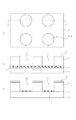
本発明の電子放出素子を同一の基体表面上を複数配列することによって、例えば、電子源や画像表示装置を構成することができる。 By arranging a plurality of the electron-emitting devices of the present invention on the same substrate surface, for example, an electron source or an image display device can be configured.
図4を用いて、本発明の電子放出素子を複数配して得られる電子源について説明する。図4において、1は基体、42はX方向配線、43はY方向配線、44は本発明の電子放出素子である。 An electron source obtained by arranging a plurality of electron-emitting devices of the present invention will be described with reference to FIG. In FIG. 4, 1 is a substrate, 42 is an X-direction wiring, 43 is a Y-direction wiring, and 44 is an electron-emitting device of the present invention.
X方向配線42は、Dx1、Dx2、…Dxmのm本の配線からなり、真空蒸着法、印刷法、スパッタ法等を用いて形成された導電性材料(典型的には金属)で構成することができる。配線の材料、膜厚、幅は適宜設計される。Y方向配線43は、Dy1、Dy2、…Dynのn本の配線からなり、X方向配線42と同様に形成される。これらm本のX方向配線42とn本のY方向配線43との間には、不図示の層間絶縁層が設けられており、両者を電気的に分離している。ここで、m及びnは共に正の整数である。不図示の層間絶縁層は、真空蒸着法、印刷法、スパッタ法等を用いて形成された酸化シリコン等で構成される。
The
電子放出素子44を構成する、第1の電極(カソ―ド電極)2はm本のX方向配線42のうちの一つに接続され、第2の電極(ゲート電極)8はn本のY方向配線43のうちの一つに電気的に接続される。
The first electrode (cathode electrode) 2 constituting the electron-emitting device 44 is connected to one of the m X-directional wirings 42, and the second electrode (gate electrode) 8 is composed of n Y electrodes. It is electrically connected to one of the
X方向配線42、Y方向配線43、及び第1の電極及び第2の電極を構成する材料は、その構成元素の一部或いは全部が同一であっても、またそれぞれ異なっていても良い。第1の電極及び第2の電極を構成する材料と配線材料が同一である場合には、X方向配線42、Y方向配線43は、それぞれ第1の電極或いは第2の電極ということもできる。
The materials constituting the
X方向配線42には、X方向に配列した電子放出素子44の行を選択するための、走査信号を印加する不図示の走査信号印加手段が接続される。一方、Y方向配線43には、Y方向に配列した電子放出素子44の各列に変調信号を印加するための、不図示の変調信号発生手段が接続される。各電子放出素子に印加される駆動電圧は、当該素子に印加される走査信号と変調信号の差電圧として定義される。
The
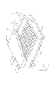
上記構成においては、個別の電子放出素子を選択し、独立に駆動可能とすることができる。このようなマトリクス配置の電子源を用いて構成した画像表示装置について、図5を用いて説明する。図5は、画像表示装置を構成する表示パネル57の一例を示す模式図である。
In the above configuration, individual electron-emitting devices can be selected and driven independently. An image display apparatus configured using such a matrix-arranged electron source will be described with reference to FIG. FIG. 5 is a schematic diagram showing an example of the
図5において、1は電子源を備える基体(「リアプレート」と呼ぶ場合もある)である。56は、透明な基体53と、その内面に配置された蛍光体などの電子線の照射によって発光する発光体からなる発光体膜54と、アノード電極としての導電性膜(メタルバックと呼ぶ場合もある)55とが設けられたフェースプレートである。52は支持枠であり、支持枠52には、リアプレート1、フェースプレート56がフリットガラス等の接着剤を用いて接続(封着)されている。57は外囲器(気密容器)であり、フェースプレートとリアプレートと支持枠とを封着することで構成されている。フェースプレート56とリアプレート1との間に、スペーサーとよばれる不図示の支持体を設置することにより、大気圧に対して十分な強度をもつ外囲器57を構成することもできる。
In FIG. 5,
また、図5を用いて説明した本発明の外囲器(表示パネル)(57)を用いて情報表示再生装置を構成することができる。 Moreover, an information display reproducing | regenerating apparatus can be comprised using the envelope (display panel) (57) of this invention demonstrated using FIG.
具体的には、受信装置と、受信した信号を選曲するチューナーと、選曲した信号に含まれる信号を、ディスプレイパネル(57)に出力してディスプレイパネル57のスクリーンに表示または再生させる。上記受信装置は、テレビジョン放送などの放送信号を受信することができる。また、上記選曲した信号に含まれる信号としては、映像情報、文字情報および音声情報の少なくとも1つを指す。尚、上記「スクリーン」は、図5で示したディスプレイパネル(57)においては、発光体膜(54)に相当すると言うことができる。この構成によりテレビジョンなどの情報表示再生装置を構成することができる。勿論、放送信号がエンコードされている場合には、本発明の情報表示再生装置はデコーダーも含むことができる。また、音声信号については、別途設けたスピーカーなどの音声再生手段に出力して、ディスプレイパネル(57)に表示される映像情報や文字情報と同期させて再生する。
Specifically, the receiving device, the tuner for selecting the received signal, and the signal included in the selected signal are output to the display panel (57) and displayed or reproduced on the screen of the
また、映像情報または文字情報をディスプレイパネル(57)に出力してスクリーンに表示および/あるいは再生させる方法としては、例えば以下のように行うことができる。まず、受信した映像情報や文字情報から、ディスプレイパネル(57)の各画素に対応した画像信号を生成する。そして生成した画像信号を、ディスプレイパネル(C11)の駆動回路(C12)に入力する。そして、駆動回路に入力された画像信号に基づいて、駆動回路からディスプレイパネル(57)内の各電子放出素子に印加する電圧を制御して、画像を表示する。 As a method of outputting video information or character information to the display panel (57) to display and / or reproduce it on the screen, for example, the following can be performed. First, an image signal corresponding to each pixel of the display panel (57) is generated from the received video information and character information. Then, the generated image signal is input to the drive circuit (C12) of the display panel (C11). Based on the image signal input to the drive circuit, the voltage applied from the drive circuit to each electron-emitting device in the display panel (57) is controlled to display an image.
図12は、本発明の情報表示再生装置の一例であるテレビジョン装置のブロック図である。受信回路(C20)は、チューナーやデコーダ等からなり、衛星放送や地上波等のテレビ信号、インターネットなどのネットワークを介したデータ放送等を受信し、復号化した映像データをI/F部(インターフェース部)(C30)に出力する。I/F部(C30)は、映像データを表示装置の表示フォーマットに変換して上記ディスプレイパネル(C11)に画像データを出力する。画像表示装置(C10)は、ディスプレイパネル(C11)、駆動回路(C12)及び制御回路(C13)を含む。制御回路は、入力した画像データに表示パネルに適した補正処理等の画像処理を施すともに、駆動回路(C12)に画像データ及び各種制御信号を出力する。駆動回路(C12)は、入力された画像データに基づいて、ディスプレイパネル(C11)の各配線(図5のDx1〜Dxm、Dy1〜Dyn参照)に駆動信号を出力し、テレビ映像が表示される。受信回路(C20)とI/F部(C30)は、セットトップボックス(STB)として画像表示装置(C10)とは別の筐体に収められていてもよいし、また画像表示装置(C10)と同一の筐体に収められていてもよい。 FIG. 12 is a block diagram of a television apparatus which is an example of the information display / reproduction apparatus of the present invention. The receiving circuit (C20) is composed of a tuner, a decoder, etc., and receives satellite broadcasting, terrestrial TV signals, data broadcasting via a network such as the Internet, etc. Part) (C30). The I / F unit (C30) converts the video data into the display format of the display device and outputs the image data to the display panel (C11). The image display device (C10) includes a display panel (C11), a drive circuit (C12), and a control circuit (C13). The control circuit performs image processing such as correction processing suitable for the display panel on the input image data, and outputs the image data and various control signals to the drive circuit (C12). Based on the input image data, the drive circuit (C12) outputs a drive signal to each wiring (see Dx1 to Dxm and Dy1 to Dyn in FIG. 5) of the display panel (C11), and a television image is displayed. . The receiving circuit (C20) and the I / F unit (C30) may be housed in a separate housing from the image display device (C10) as a set top box (STB), or the image display device (C10). May be housed in the same housing.
また、インターフェースには、プリンター、デジタルビデオカメラ、デジタルカメラ、ハードディスクドライブ(HDD)、デジタルビデオディスク(DVD)などの画像記録装置や画像出力装置に接続することができる構成とすることもできる。そして、このようにすれば、画像記録装置に記録された画像をディスプレイパネル(C11)に表示させることもできる。また、ディスプレイパネル(C11)に表示させた画像を、必要に応じて加工し、画像出力装置に出力させることもできる情報表示再生装置(またはテレビジョン)を構成することができる。 Further, the interface can be configured to be connected to an image recording apparatus or an image output apparatus such as a printer, a digital video camera, a digital camera, a hard disk drive (HDD), or a digital video disk (DVD). And if it does in this way, the image recorded on the image recording device can also be displayed on a display panel (C11). In addition, it is possible to configure an information display / playback apparatus (or television) that can process an image displayed on the display panel (C11) as necessary and output the processed image to an image output apparatus.
ここで述べた情報表示再生装置の構成は、一例であり、本発明の技術思想に基づいて種々の変形が可能である。また、本発明の情報表示再生装置は、テレビ会議システムやコンピュータ等のシステムと接続することで、様々な情報表示再生装置を構成することができる。 The configuration of the information display / reproduction apparatus described here is an example, and various modifications can be made based on the technical idea of the present invention. In addition, the information display / playback apparatus of the present invention can be configured with various information display / playback apparatuses by connecting to a system such as a video conference system or a computer.
以下本発明の実施例を詳細に説明する。 Examples of the present invention will be described in detail below.
(実施例1)
図2に示した電子放出素子を図6に示した工程に従って作製した。
Example 1
The electron-emitting device shown in FIG. 2 was fabricated according to the process shown in FIG.
(工程1)
基体1として石英基板を用い、これを十分に洗浄を行った後、基体1上に、多数の柱状領域3を形成するために、以下に示す(条件1)で、スパッタ法により、TiN膜を100nmの厚さで成膜した。下記(条件1)における雰囲気ガスは、ArガスとN2ガスとを9:1の割合で混合したガスを用いた。
(Process 1)
A quartz substrate is used as the
(条件1)
Rf電源 : 13.56MHz
Rf出力 : 8W/cm2
雰囲気ガス圧 : 1.2Pa
ターゲット : Ti
成膜されたTiN膜は、図6(a)に示す様に、多数の柱状領域3から構成されており、柱状領域3の平均直径Wは、30nmであり、その抵抗率ρ3は10−4Ω・cmであった。平均直径Wは、走査型電子顕微鏡で、成膜したTiN膜の表面を20万倍の倍率で撮影し、その写真で直径を測長し、平均化した数値である。
(Condition 1)
Rf power supply: 13.56 MHz
Rf output: 8 W / cm 2
Atmospheric gas pressure: 1.2Pa
Target: Ti
As shown in FIG. 6A, the formed TiN film is composed of a large number of
尚、このように、成膜条件を制御することで、多数の柱状領域3を簡易に形成できる材料としては、Ti、TiN、Ta、TaN、Al、AlN、TiAlNが挙げられる。
In addition, Ti, TiN, Ta, TaN, Al, AlN, and TiAlN are mentioned as materials that can easily form a large number of
(工程2)
次に、大気雰囲気(酸素含有雰囲気)のオーブンの中に上記工程1を経た基体1を入れ、350℃で1時間の加熱を行った。すると、図6(b)のように隣り合うTiNの柱状領域3の間(柱状領域3の側面)にTiの酸化物を主体とした第2の領域4が形成された。また同時に、柱状領域3の表面にTiの酸化物層12が形成された。
(Process 2)
Next, the
TEM(透過型電子顕微鏡)によって観察すると、隣合う2つの柱状領域3の間に領域4が存在することを観察することができた。領域4をEDX(エネルギー分散型X線分析装置)で定性分析すると、Tiと酸素とNの存在が認められ、領域4が酸化物であることが確認できた。また、ESCA(X線光電子分光分析法)で測定したところTiの酸化物とTiの窒化物の存在が確認された。また層4の幅W‘−Wは、14nmであり、その抵抗率ρ4は109Ω・cmであった。
When observed with a TEM (transmission electron microscope), it was observed that the region 4 was present between two adjacent
(工程3)
ドライエッチングにより、柱状領域3の表面の酸化層12を除去し、導電層2の酸化されていない表面を露出させる(図6(c)。つまり、領域3と領域4とを露出させる。この時、隣り合う複数のTiNの柱状領域3の間の、酸化物層である領域4は除去せず、隣り合う柱状領域3の間を埋めたままとした。
(Process 3)
The
(工程4)
ついでスパッタ法によりコバルトを含んだ炭素膜5を導電層2上に12nm堆積した(図6(d))。
(Process 4)
Next, a
炭素膜15の主体としてはアモルファスカーボンを用いた。従って、この工程で形成した膜15は、アモルファスカーボンを主成分とし、コバルトを含む膜と言い換えることができる。このコバルトを含む膜の比抵抗は、103Ω・cmであった。 Amorphous carbon was used as the main body of the carbon film 15. Therefore, the film 15 formed in this step can be rephrased as a film containing amorphous carbon as a main component and containing cobalt. The specific resistance of the film containing cobalt was 10 3 Ω · cm.
(工程5)
炭素膜15上に、プラズマCVD法により絶縁層7としてSiO2を1000nm成膜した(図6(e))。
(Process 5)
A 1000 nm thick SiO2 film was formed as an insulating layer 7 on the carbon film 15 by plasma CVD (FIG. 6E).
(工程6)
絶縁層7上に、ゲート電極8として、Ptを100nmの厚さになるように成膜した(図6(f))。
(Step 6)
On the insulating layer 7, a Pt film was formed to a thickness of 100 nm as the gate electrode 8 (FIG. 6F).
(工程7)
次いで、ゲート電極8上に、ポジ型フォトレジストをスピンコートし、フォトマスクパターン(円形)を露光、現像し、不図示のマスクパターンを形成した。マスクパターンは、円形の開口を備えている。このときの開口径は、1.5μmとした。尚、開口の数は、図7に示した様に複数個形成してもよく、特に限定されるものではない。
(Step 7)
Next, a positive photoresist was spin-coated on the
(工程8)
ドライエッチングにより、炭素膜5の表面が露出するまで、前記マスクパターンの開口の直下に位置するゲート電極8および絶縁層7をエッチングし、開口21を形成した(図6(g))。
(Process 8)
By dry etching, the
(工程9)
残ったマスクパターン(不図示)を、剥離液にて除去し、水洗を行った。
(Step 9)
The remaining mask pattern (not shown) was removed with a stripping solution and washed with water.
(工程10)
次に、アセチレンと水素の混合ガス雰囲気中で、基体1を550℃で300分間熱処理を行った。この熱処理でコバルトが凝集し、コバルト粒子6を内包する炭素膜5(即ち電子放出膜5)を形成した(図6(h))。
(Process 10)
Next, the
以上の工程で、実施例1の電子放出素子を完成させた。 Through the above steps, the electron-emitting device of Example 1 was completed.
このように作製した電子放出素子の電子放出特性を測定した。測定に際しては、本実施例で作製した電子放出素子を図9に示すように、電子放出素子の上方に、離れて、アノード電極9を配置した。そして、アノード電極9、導電層2、ゲート電極8にそれぞれ電位を印加して、電子放出特性を測定した。
The electron emission characteristics of the electron-emitting device thus manufactured were measured. In the measurement, as shown in FIG. 9, the electron-emitting device manufactured in this example was separated from the electron-emitting device and the anode electrode 9 was disposed. Then, potentials were applied to the anode electrode 9, the
印加電圧はVa=10kV、Vb=20Vとし、電子放出膜5とアノード電極9との距離Hを2mmとした。その結果、柱状領域を備えていないTiN膜を用いた電子放出素子では、電子放出素子が、一部、基体1から剥離してしまった。一方、本実施例の電子放出素子では、基体1から電子放出膜5が剥離することもなく、安定した電子放出特性を示し、電子放出量のゆらぎも小さかった。
The applied voltages were Va = 10 kV and Vb = 20 V, and the distance H between the
また、電子放出量のゆらぎを比較するために、上記工程4で形成する炭素膜5を20nmの厚みで形成した電子放出素子1と、炭素膜5を100nmの厚みで形成した電子放出素子2も用意した。これらの電子放出素子1及び2は、上記厚み以外は、実施例1の電子放出素子の製造方法と同様の方法で形成した。
In order to compare fluctuations in the amount of electron emission, an electron-emitting
そして、実施例1の電子放出素子の電子放出量のゆらぎと、電子放出素子1及び2の電子放出量のゆらぎを比較すると、実施例1の電子放出素子と電子放出素子1との比較では実施例1の電子放出素子の方が若干優れていた。一方、電子放出素子1と電子放出素子2との比較では、電子放出素子1の方が電子放出量のゆらぎは非常に小さかった。
When the fluctuation of the electron emission amount of the electron-emitting device of Example 1 is compared with the fluctuation of the electron emission amount of the electron-emitting
この時のそれぞれのkの値は、実施例1の電子放出素子は、5.0であり、電子放出素子1は3.5であり、電子放出素子2は0.70であった。つまり、電子放出素子2は、電子放出点での電子の広がりと、それに隣接した電子放出点での電子の広がりとの重なりが、I0の61%の地点で起こっており、電子放出ゆらぎは、特に大きかった。
The values of k at this time were 5.0 for the electron-emitting device of Example 1, 3.5 for the electron-emitting
これは、電子放出素子2では、先述した式(1)を満たしておらず、領域3から流れ込む電子の広がりが、隣の領域3から流れ込む電子の広がりと実質的に重なってしまうためであると推察される。このように、電子放出膜5の膜厚が、(式1)を満たさないと、電子放出量のゆらぎが顕著に増大する傾向になる。
This is because the electron-emitting
また、上記工程1における条件を下記(条件2)に変更して、柱状領域3を備えない導電層2を形成し、続いて、上記工程2、3を行わずに、上記工程4〜10を行って、比較用の電子放出素子3を作製した。尚、下記(条件2)における雰囲気ガスは、ArとN2ガスを9:1の混合ガスであった。
Moreover, the conditions in the said
(条件2)
Rf電源 : 13.56MHz
Rf出力 : 8W/cm2
ガス圧 : 0.4Pa
ターゲット : Ti
上記条件2で成膜されたTiN膜は、柱状領域の見られないバルク状の膜であった。そして、比較用の電子放出素子3の電子放出量のゆらぎは、実施例1の電子放出素子に比べて非常に大きかった。また、同じ製造工程で作成した他のサンプルでは、電子放出膜が基体から剥離してしまった。また、別のサンプルでは、電子放出膜中の金属の含有量が実施例1で作成した電子放出膜に比べて大幅に減少していた。この傾向は、上記工程2および工程3を行わずに作成した電子放出膜にも同様に見られた。
(Condition 2)
Rf power supply: 13.56 MHz
Rf output: 8 W / cm 2
Gas pressure: 0.4 Pa
Target: Ti
The TiN film formed under the
(実施例2)
本実施例では、図2に示した電子放出素子を図8に示した工程に従って作製した。尚、本実施例2の電子放出素子は、実施例1に対して、電子放出膜5を開口21内部にのみ配置した構成の電子放出素子である。
(Example 2)
In this example, the electron-emitting device shown in FIG. 2 was produced according to the process shown in FIG. The electron-emitting device of Example 2 is an electron-emitting device having a configuration in which the electron-emitting
(工程1)
実施例1の工程1と同様に、基体1上に多数のTiNからなる柱状領域3を形成した(図8(a))。柱状領域3の平均直径は、30nmであり、抵抗率ρ3は10−4Ω・cmであった。
(Process 1)
Similar to Step 1 of Example 1, a
(工程2)
次に、オゾン雰囲気のアッシング装置の中に基体1を入れ、オゾンアッシングを行ったところ、隣り合う複数のTiNの柱状領域3の間(柱状領域3の側面)にTiの酸化物を主体とした第2の領域4が形成された。また同時に、柱状領域3の表面にTiの酸化物層12が形成された(図8(b))。
(Process 2)
Next, the
TEM(透過型電子顕微鏡)によって観察すると、柱状構造体3と隣り合う柱状構造体3の間の領域4が観察された。領域4をEDX(エネルギー分散型X線分析装置)で定性分析すると酸素の存在が認められ、領域4が酸化物であることが確認でき、また、領域4の幅は14nmであり、その比抵抗は109Ω・cmであった。
When observed with a TEM (transmission electron microscope), a region 4 between the
(工程3)
実施例1の工程3と同様に、ドライエッチングで、酸化層12を除去し導電層2の酸化されていない表面を露出させる(図8(c))。
(Process 3)
Similar to Step 3 of Example 1, the
(工程4)
導電層2上に、プラズマCVD法により絶縁層7としてSiO2を1000nm成膜した(図8(d))。
(Process 4)
On the
(工程5)
絶縁層7上に、ゲート電極8として、Ptを100nmの厚さになるように成膜した(図8(e))。
(Process 5)
On the insulating layer 7, a Pt film was formed to a thickness of 100 nm as the gate electrode 8 (FIG. 8E).
(工程6)
次いで、ゲート電極8上に、実施例1の工程7と同様に不図示のマスクパターンを形成した。マスクパターンは、円形の開口を備えており、開口径は、1.5μmとした。
(Step 6)
Next, a mask pattern (not shown) was formed on the
(工程7)
ドライエッチングにより、導電層2の表面が露出するまで、前記マスクパターンの開口の直下に位置するゲート電極8及び絶縁層7をエッチングし、開口21を形成した(図8(f))。
(Step 7)
By dry etching, the
(工程8)
ついでスパッタ法によりコバルトを含んだ炭素膜5を開口21内に露出した導電層2上に12nm堆積した(図8(g))。このコバルトを含む膜5の比抵抗は、103Ω・cmであった。
(Process 8)
Next, a
(工程9)
残ったマスクパターン(不図示)を、剥離液にて除去し、水洗を行った。
(Step 9)
The remaining mask pattern (not shown) was removed with a stripping solution and washed with water.
(工程10)
次に、実施例1の工程10と同様の手法で、コバルト粒子6を内包する炭素膜5(即ち電子放出膜5)を形成した(図8(h))。
(Process 10)
Next, the
以上の工程で、実施例2の電子放出素子を完成させた。 Through the above steps, the electron-emitting device of Example 2 was completed.
また、実施例2で作製した電子放出素子の電子放出特性を実施例1と同様に図10に示すようにアノード電極9を配置して測定した。印加電圧はVa=10kV、Vb=20Vで、電子放出膜3とアノード電極8との距離Hを2mmとした。
Further, the electron emission characteristics of the electron-emitting device manufactured in Example 2 were measured by arranging the anode electrode 9 as shown in FIG. The applied voltages were Va = 10 kV and Vb = 20 V, and the distance H between the
その結果、基体1から電子放出素子が剥離することもなく、安定した電子放出特性を示し、さらに実施例1と同様に電子放出量のゆらぎの小さい電子放出素子を形成することができた。
As a result, it was possible to form an electron-emitting device that showed stable electron-emitting characteristics without peeling off the electron-emitting device from the
(実施例3)
上記実施例2で作製した電子放出素子を用いて図5に示す画像表示装置57を作製した。
(Example 3)
An
実施例2で示した電子放出素子を、X方向に100個、Y方向に100個、マトリクス状に配置した。配線は図5に示したようにX方向配線42(Dx1〜Dxm)を導電層2に接続し、Y方向配線43(Dy1〜Dyn)をゲート電極8に接続した。各電子放出素子44の上方には蛍光体層54とアノード電極であるメタルバック55を配置した。図5では、1つの電子放出素子44に開口21が一つ形成されている例を示しているが、開口の数は一つに限定されるものではなく、複数の開口を備えていても構わない。
100 electron-emitting devices shown in Example 2 were arranged in a matrix, 100 in the X direction and 100 in the Y direction. As shown in FIG. 5, the X direction wiring 42 (Dx1 to Dxm) was connected to the
外囲器57を封着するために接着剤としてインジウムを用いてリアプレート1とフェースプレート56とを支持枠52を間に挟んで封着した。この結果、単純マトリクス駆動が可能で、高精細で、輝度ばらつきの少ない、画像表示装置が形成できた。
In order to seal the
1 基体
2 導電層
3 第1の領域
4 第2の領域
5 電子放出膜
6 粒子
100 柱状構造体
101 第3の領域
DESCRIPTION OF
Claims (19)
前記導電層が、(A)複数の第1領域と、(B)複数の第1領域の各々の間に設けられた、前記第1領域よりも高抵抗な第2領域とを、少なくとも有する表面を備えており、
前記電子放出膜が、前記導電層の前記表面を覆っている、ことを特徴とする電子放出素子。 An electron-emitting device comprising a conductive layer and an electron-emitting film disposed on the conductive layer,
The surface at which the conductive layer has at least (A) a plurality of first regions and (B) a second region provided between each of the plurality of first regions and having a higher resistance than the first region. With
The electron-emitting device, wherein the electron-emitting film covers the surface of the conductive layer.
(i)(a)導電性の複数の柱状領域を具備する導電層と、(b)該導電層上に配置された、金属を含有する層と、を備える構造体を用意する工程、
(ii)前記構造体を加熱する工程、とを有することを特徴とする電子放出素子の製造方法。 A method for manufacturing an electron-emitting device comprising a conductive layer and an electron-emitting film disposed on the conductive layer,
(I) a step of preparing a structure including (a) a conductive layer including a plurality of conductive columnar regions; and (b) a layer containing a metal disposed on the conductive layer.
(Ii) a step of heating the structure, and a method for manufacturing an electron-emitting device.
Priority Applications (3)
| Application Number | Priority Date | Filing Date | Title |
|---|---|---|---|
| JP2006117730A JP2007294126A (en) | 2006-04-21 | 2006-04-21 | Electron emission element and manufacturing method thereof, electron source, and image display |
| US11/697,914 US7973463B2 (en) | 2006-04-21 | 2007-04-09 | Electron-emitting device, electron source, image display apparatus and method of fabricating electron-emitting device |
| CN2007101008617A CN101060048B (en) | 2006-04-21 | 2007-04-20 | Electron-emitting device, image display apparatus and image display and reproduction device |
Applications Claiming Priority (1)
| Application Number | Priority Date | Filing Date | Title |
|---|---|---|---|
| JP2006117730A JP2007294126A (en) | 2006-04-21 | 2006-04-21 | Electron emission element and manufacturing method thereof, electron source, and image display |
Publications (2)
| Publication Number | Publication Date |
|---|---|
| JP2007294126A true JP2007294126A (en) | 2007-11-08 |
| JP2007294126A5 JP2007294126A5 (en) | 2009-11-26 |
Family
ID=38660589
Family Applications (1)
| Application Number | Title | Priority Date | Filing Date |
|---|---|---|---|
| JP2006117730A Withdrawn JP2007294126A (en) | 2006-04-21 | 2006-04-21 | Electron emission element and manufacturing method thereof, electron source, and image display |
Country Status (3)
| Country | Link |
|---|---|
| US (1) | US7973463B2 (en) |
| JP (1) | JP2007294126A (en) |
| CN (1) | CN101060048B (en) |
Families Citing this family (17)
| Publication number | Priority date | Publication date | Assignee | Title |
|---|---|---|---|---|
| JP2007214032A (en) * | 2006-02-10 | 2007-08-23 | Canon Inc | Electron emitting element, electron source, and manufacturing method of image display device |
| JP2008218195A (en) * | 2007-03-05 | 2008-09-18 | Canon Inc | Electron source, image display device, and data display reproduction device |
| JP2009032443A (en) * | 2007-07-25 | 2009-02-12 | Canon Inc | Electron emission element, electron source, image display device, and information display reproduction system |
| JP2009104916A (en) * | 2007-10-24 | 2009-05-14 | Canon Inc | Electron emitting element, electron source, image display device, and manufacturing method of electron emitting element |
| JP2009110755A (en) * | 2007-10-29 | 2009-05-21 | Canon Inc | Electron emission element, electron source, image display device, and method of manufacturing electron emission element |
| JP2009117203A (en) * | 2007-11-07 | 2009-05-28 | Canon Inc | Method for manufacturing electron emission device, method for manufacturing electron source, and method for manufacturing image display apparatus |
| JP2009140655A (en) * | 2007-12-04 | 2009-06-25 | Canon Inc | Electron-emitting element, electron source, image display device, and manufacturing method for electron-emitting element |
| JP2009146639A (en) * | 2007-12-12 | 2009-07-02 | Canon Inc | Electron emission device, electron source, image display apparatus, and method for manufacturing electron emission device |
| JP2009146751A (en) * | 2007-12-14 | 2009-07-02 | Canon Inc | Electron emission device, electron source, and image display apparatus |
| TWI375984B (en) * | 2008-09-19 | 2012-11-01 | Univ Nat Taiwan | Nano-hole array in conductor element for improving the contact conductance |
| CN102681397B (en) * | 2011-03-09 | 2016-08-31 | 富士施乐株式会社 | Charging device, for the box of image processing system and image processing system |
| CN104681374B (en) * | 2015-03-03 | 2017-03-01 | 中国科学院半导体研究所 | The electronic receipt structure of AlN cold cathode surface oxidation can be reduced |
| CN104658829B (en) * | 2015-03-03 | 2017-05-03 | 中国科学院半导体研究所 | AlN thin film type cold cathode adopting stair-shaped component gradient |
| CN104658831B (en) * | 2015-03-03 | 2017-03-08 | 中国科学院半导体研究所 | Miniaturization, integrated silicon substrate Flied emission receiving device |
| CN104658830B (en) * | 2015-03-03 | 2017-05-03 | 中国科学院半导体研究所 | AlN cold cathode structure on SiC substrate |
| CN108796441B (en) * | 2018-06-06 | 2020-03-03 | 中国科学院宁波材料技术与工程研究所 | Light absorption coating film, preparation method and application thereof |
| US10921268B1 (en) * | 2019-09-09 | 2021-02-16 | Fei Company | Methods and devices for preparing sample for cryogenic electron microscopy |
Family Cites Families (22)
| Publication number | Priority date | Publication date | Assignee | Title |
|---|---|---|---|---|
| FR2623013A1 (en) * | 1987-11-06 | 1989-05-12 | Commissariat Energie Atomique | ELECTRO SOURCE WITH EMISSIVE MICROPOINT CATHODES AND FIELD EMISSION-INDUCED CATHODOLUMINESCENCE VISUALIZATION DEVICE USING THE SOURCE |
| US5559389A (en) * | 1993-09-08 | 1996-09-24 | Silicon Video Corporation | Electron-emitting devices having variously constituted electron-emissive elements, including cones or pedestals |
| FR2713394B1 (en) | 1993-11-29 | 1996-11-08 | Futaba Denshi Kogyo Kk | Field emission type electron source. |
| CA2299957C (en) * | 1993-12-27 | 2003-04-29 | Canon Kabushiki Kaisha | Electron-emitting device and method of manufacturing the same as well as electron source and image-forming apparatus |
| JP2809078B2 (en) * | 1993-12-28 | 1998-10-08 | 日本電気株式会社 | Field emission cold cathode and method of manufacturing the same |
| JP3387617B2 (en) * | 1994-03-29 | 2003-03-17 | キヤノン株式会社 | Electron source |
| US5473218A (en) | 1994-05-31 | 1995-12-05 | Motorola, Inc. | Diamond cold cathode using patterned metal for electron emission control |
| US5569975A (en) * | 1994-11-18 | 1996-10-29 | Texas Instruments Incorporated | Cluster arrangement of field emission microtips |
| US5837331A (en) * | 1996-03-13 | 1998-11-17 | Motorola, Inc. | Amorphous multi-layered structure and method of making the same |
| JPH11213866A (en) * | 1998-01-22 | 1999-08-06 | Sony Corp | Electron-emitting device, its manufacture, and display apparatus using the device |
| US6794805B1 (en) * | 1998-05-26 | 2004-09-21 | Matsushita Electric Works, Ltd. | Field emission electron source, method of producing the same, and use of the same |
| US6350999B1 (en) * | 1999-02-05 | 2002-02-26 | Matsushita Electric Industrial Co., Ltd. | Electron-emitting device |
| JP4196490B2 (en) * | 1999-05-18 | 2008-12-17 | ソニー株式会社 | Cathode panel for cold cathode field emission display, cold cathode field emission display, and method for manufacturing cathode panel for cold cathode field emission display |
| JP3581289B2 (en) | 2000-03-06 | 2004-10-27 | シャープ株式会社 | Field emission electron source array and method of manufacturing the same |
| US20020117960A1 (en) * | 2000-09-01 | 2002-08-29 | Yi Jay J.L. | Field emission wafer and process for making same for use in field emission display devices |
| JP4011863B2 (en) | 2001-05-30 | 2007-11-21 | キヤノン株式会社 | Electron emitting device, electron source, and image forming apparatus using the same |
| JP3535871B2 (en) * | 2002-06-13 | 2004-06-07 | キヤノン株式会社 | Electron emitting device, electron source, image display device, and method of manufacturing electron emitting device |
| JP4154356B2 (en) | 2003-06-11 | 2008-09-24 | キヤノン株式会社 | Electron emitting device, electron source, image display device, and television |
| JP3840251B2 (en) * | 2004-03-10 | 2006-11-01 | キヤノン株式会社 | ELECTRON EMITTING ELEMENT, ELECTRON SOURCE, IMAGE DISPLAY DEVICE, INFORMATION DISPLAY REPRODUCING DEVICE USING THE IMAGE DISPLAY DEVICE, AND METHOD FOR MANUFACTURING THE SAME |
| KR20060104655A (en) * | 2005-03-31 | 2006-10-09 | 삼성에스디아이 주식회사 | Electron emission device |
| JP2007214032A (en) | 2006-02-10 | 2007-08-23 | Canon Inc | Electron emitting element, electron source, and manufacturing method of image display device |
| KR20080044702A (en) * | 2006-11-17 | 2008-05-21 | 삼성에스디아이 주식회사 | Electron emission device, manufacturing method of the same, and electron emission display using the same |
-
2006
- 2006-04-21 JP JP2006117730A patent/JP2007294126A/en not_active Withdrawn
-
2007
- 2007-04-09 US US11/697,914 patent/US7973463B2/en not_active Expired - Fee Related
- 2007-04-20 CN CN2007101008617A patent/CN101060048B/en not_active Expired - Fee Related
Also Published As
| Publication number | Publication date |
|---|---|
| CN101060048A (en) | 2007-10-24 |
| CN101060048B (en) | 2010-11-03 |
| US7973463B2 (en) | 2011-07-05 |
| US20070257593A1 (en) | 2007-11-08 |
Similar Documents
| Publication | Publication Date | Title |
|---|---|---|
| JP2007294126A (en) | Electron emission element and manufacturing method thereof, electron source, and image display | |
| US7572164B2 (en) | Method for manufacturing electron-emitting device, methods for manufacturing electron source and image display device using the electron-emitting device | |
| KR100860894B1 (en) | Electron-emitting device, electron source, display apparatus and information display apparatus using the same device, and manufacturing methods of them | |
| JP3907667B2 (en) | ELECTRON EMITTING ELEMENT, ELECTRON EMITTING DEVICE, ELECTRON SOURCE USING SAME, IMAGE DISPLAY DEVICE AND INFORMATION DISPLAY REPRODUCING DEVICE | |
| US7843118B2 (en) | Electron-emitting device, electron source using the same, image display apparatus, and information displaying and reproducing apparatus | |
| KR100709174B1 (en) | Electron-emitting device, electron source, image display device and information display and reproduction apparatus using image display device, and method of manufacturing the same | |
| US8388400B2 (en) | Method of fabricating electron-emitting device and method of manufacturing image display apparatus | |
| WO2008013040A1 (en) | Electron-emitting device, electron source, and image display apparatus, and method for manufacturing the same | |
| US20110305314A1 (en) | Electron emitting device, image display apparatus using the same, radiation generation apparatus, and radiation imaging system | |
| JP2007214032A (en) | Electron emitting element, electron source, and manufacturing method of image display device | |
| US7588475B2 (en) | Field-emission electron source, method of manufacturing the same, and image display apparatus | |
| JP2009277458A (en) | Electron emitter and image display apparatus | |
| JP4401245B2 (en) | Manufacturing method of cold cathode electron source | |
| US8080932B2 (en) | Electron-emitting device, electron source, image display apparatus and method for manufacturing electron-emitting device | |
| JP2008053057A (en) | Electron emission element, method of manufacturing electron emission element, and display device with electron emission element | |
| JP2009110791A (en) | Electron emission element, electron source, image display device, and method of manufacturing electron emission element | |
| JP2005183103A (en) | Electron emission element and image display device | |
| JP2009170344A (en) | Electron emission element manufacturing method, electron emission element, electron source, and image display | |
| JP2011129484A (en) | Electron-emitting device, electron source, and image display apparatus |
Legal Events
| Date | Code | Title | Description |
|---|---|---|---|
| A621 | Written request for application examination |
Free format text: JAPANESE INTERMEDIATE CODE: A621 Effective date: 20090421 |
|
| A521 | Written amendment |
Free format text: JAPANESE INTERMEDIATE CODE: A523 Effective date: 20091007 |
|
| RD04 | Notification of resignation of power of attorney |
Free format text: JAPANESE INTERMEDIATE CODE: A7424 Effective date: 20100201 |
|
| RD01 | Notification of change of attorney |
Free format text: JAPANESE INTERMEDIATE CODE: A7421 Effective date: 20100630 |
|
| A977 | Report on retrieval |
Free format text: JAPANESE INTERMEDIATE CODE: A971007 Effective date: 20110316 |
|
| A761 | Written withdrawal of application |
Free format text: JAPANESE INTERMEDIATE CODE: A761 Effective date: 20110614 |