JP2004335533A - マルチチップパッケージ - Google Patents
マルチチップパッケージ Download PDFInfo
- Publication number
- JP2004335533A JP2004335533A JP2003125322A JP2003125322A JP2004335533A JP 2004335533 A JP2004335533 A JP 2004335533A JP 2003125322 A JP2003125322 A JP 2003125322A JP 2003125322 A JP2003125322 A JP 2003125322A JP 2004335533 A JP2004335533 A JP 2004335533A
- Authority
- JP
- Japan
- Prior art keywords
- package
- chip
- chip package
- package according
- solid
- Prior art date
- Legal status (The legal status is an assumption and is not a legal conclusion. Google has not performed a legal analysis and makes no representation as to the accuracy of the status listed.)
- Withdrawn
Links
Images


Classifications
-
- H—ELECTRICITY
- H01—ELECTRIC ELEMENTS
- H01L—SEMICONDUCTOR DEVICES NOT COVERED BY CLASS H10
- H01L2224/00—Indexing scheme for arrangements for connecting or disconnecting semiconductor or solid-state bodies and methods related thereto as covered by H01L24/00
- H01L2224/01—Means for bonding being attached to, or being formed on, the surface to be connected, e.g. chip-to-package, die-attach, "first-level" interconnects; Manufacturing methods related thereto
- H01L2224/10—Bump connectors; Manufacturing methods related thereto
- H01L2224/15—Structure, shape, material or disposition of the bump connectors after the connecting process
- H01L2224/16—Structure, shape, material or disposition of the bump connectors after the connecting process of an individual bump connector
- H01L2224/161—Disposition
- H01L2224/16151—Disposition the bump connector connecting between a semiconductor or solid-state body and an item not being a semiconductor or solid-state body, e.g. chip-to-substrate, chip-to-passive
- H01L2224/16221—Disposition the bump connector connecting between a semiconductor or solid-state body and an item not being a semiconductor or solid-state body, e.g. chip-to-substrate, chip-to-passive the body and the item being stacked
- H01L2224/16225—Disposition the bump connector connecting between a semiconductor or solid-state body and an item not being a semiconductor or solid-state body, e.g. chip-to-substrate, chip-to-passive the body and the item being stacked the item being non-metallic, e.g. insulating substrate with or without metallisation
-
- H—ELECTRICITY
- H01—ELECTRIC ELEMENTS
- H01L—SEMICONDUCTOR DEVICES NOT COVERED BY CLASS H10
- H01L2224/00—Indexing scheme for arrangements for connecting or disconnecting semiconductor or solid-state bodies and methods related thereto as covered by H01L24/00
- H01L2224/01—Means for bonding being attached to, or being formed on, the surface to be connected, e.g. chip-to-package, die-attach, "first-level" interconnects; Manufacturing methods related thereto
- H01L2224/26—Layer connectors, e.g. plate connectors, solder or adhesive layers; Manufacturing methods related thereto
- H01L2224/31—Structure, shape, material or disposition of the layer connectors after the connecting process
- H01L2224/32—Structure, shape, material or disposition of the layer connectors after the connecting process of an individual layer connector
- H01L2224/321—Disposition
- H01L2224/32135—Disposition the layer connector connecting between different semiconductor or solid-state bodies, i.e. chip-to-chip
- H01L2224/32145—Disposition the layer connector connecting between different semiconductor or solid-state bodies, i.e. chip-to-chip the bodies being stacked
-
- H—ELECTRICITY
- H01—ELECTRIC ELEMENTS
- H01L—SEMICONDUCTOR DEVICES NOT COVERED BY CLASS H10
- H01L2224/00—Indexing scheme for arrangements for connecting or disconnecting semiconductor or solid-state bodies and methods related thereto as covered by H01L24/00
- H01L2224/01—Means for bonding being attached to, or being formed on, the surface to be connected, e.g. chip-to-package, die-attach, "first-level" interconnects; Manufacturing methods related thereto
- H01L2224/42—Wire connectors; Manufacturing methods related thereto
- H01L2224/47—Structure, shape, material or disposition of the wire connectors after the connecting process
- H01L2224/48—Structure, shape, material or disposition of the wire connectors after the connecting process of an individual wire connector
- H01L2224/4805—Shape
- H01L2224/4809—Loop shape
- H01L2224/48091—Arched
-
- H—ELECTRICITY
- H01—ELECTRIC ELEMENTS
- H01L—SEMICONDUCTOR DEVICES NOT COVERED BY CLASS H10
- H01L2224/00—Indexing scheme for arrangements for connecting or disconnecting semiconductor or solid-state bodies and methods related thereto as covered by H01L24/00
- H01L2224/01—Means for bonding being attached to, or being formed on, the surface to be connected, e.g. chip-to-package, die-attach, "first-level" interconnects; Manufacturing methods related thereto
- H01L2224/42—Wire connectors; Manufacturing methods related thereto
- H01L2224/47—Structure, shape, material or disposition of the wire connectors after the connecting process
- H01L2224/48—Structure, shape, material or disposition of the wire connectors after the connecting process of an individual wire connector
- H01L2224/481—Disposition
- H01L2224/48151—Connecting between a semiconductor or solid-state body and an item not being a semiconductor or solid-state body, e.g. chip-to-substrate, chip-to-passive
- H01L2224/48221—Connecting between a semiconductor or solid-state body and an item not being a semiconductor or solid-state body, e.g. chip-to-substrate, chip-to-passive the body and the item being stacked
- H01L2224/48225—Connecting between a semiconductor or solid-state body and an item not being a semiconductor or solid-state body, e.g. chip-to-substrate, chip-to-passive the body and the item being stacked the item being non-metallic, e.g. insulating substrate with or without metallisation
- H01L2224/48227—Connecting between a semiconductor or solid-state body and an item not being a semiconductor or solid-state body, e.g. chip-to-substrate, chip-to-passive the body and the item being stacked the item being non-metallic, e.g. insulating substrate with or without metallisation connecting the wire to a bond pad of the item
-
- H—ELECTRICITY
- H01—ELECTRIC ELEMENTS
- H01L—SEMICONDUCTOR DEVICES NOT COVERED BY CLASS H10
- H01L2224/00—Indexing scheme for arrangements for connecting or disconnecting semiconductor or solid-state bodies and methods related thereto as covered by H01L24/00
- H01L2224/73—Means for bonding being of different types provided for in two or more of groups H01L2224/10, H01L2224/18, H01L2224/26, H01L2224/34, H01L2224/42, H01L2224/50, H01L2224/63, H01L2224/71
- H01L2224/732—Location after the connecting process
- H01L2224/73251—Location after the connecting process on different surfaces
- H01L2224/73253—Bump and layer connectors
-
- H—ELECTRICITY
- H01—ELECTRIC ELEMENTS
- H01L—SEMICONDUCTOR DEVICES NOT COVERED BY CLASS H10
- H01L2924/00—Indexing scheme for arrangements or methods for connecting or disconnecting semiconductor or solid-state bodies as covered by H01L24/00
- H01L2924/19—Details of hybrid assemblies other than the semiconductor or other solid state devices to be connected
- H01L2924/191—Disposition
- H01L2924/19101—Disposition of discrete passive components
- H01L2924/19107—Disposition of discrete passive components off-chip wires
Landscapes
- Transforming Light Signals Into Electric Signals (AREA)
- Solid State Image Pick-Up Elements (AREA)
Abstract
【課題】小型、低価格な固体撮像素子の実装方法を提供する。
【解決手段】板金凹部にフレキシブルプリント板を貼り合わせ、固体撮像素子と周辺回路素子を収納したパッケージを構成する。
【選択図】 図1
【解決手段】板金凹部にフレキシブルプリント板を貼り合わせ、固体撮像素子と周辺回路素子を収納したパッケージを構成する。
【選択図】 図1
Description
【0001】
【発明の属する技術分野】
本発明はCCD、CMOSなどの固体撮像素と周辺回路部品とを一体に実装するマルチチップパッケージに関するものである。
【0002】
【従来の技術】
近年、デジタルビデオカメラ、デジタルスチルカメラなど映像・画像の入力機器(以下、機器と略す)、が急速に普及している。そして、これらの機器ではより高機能化、小型化と低価格化が並行して求められ、固体撮像素子を機器へ搭載するための実装方法にも一層の小型化、低価格化が求められている。
【0003】
そのような課題を解決する目的で、固体撮像素子のみならず、その周辺に実装すべき素子も一体化するマルチチップパッケージが多く提案されている。
【0004】
例えば図5に示す特開平10−084509号公報(松下電子工業株式会社)では、セラミックパッケージの内部に固体撮像素子及び周辺回路素子を搭載した基板を収納し、ガラスなどの蓋で封止する技術が開示されている。
【0005】
また、図6の特開平11−261044号公報(松下電器産業株式会社)では、基板に周辺回路素子をフリップチップ実装し、その裏面に固体撮像素子を接着した後、周囲を封止する技術が開示されている。
【0006】
しかしながら、上記の技術には以下のごとき欠点がある。
【0007】
すなわち、特開平10−084509号公報では固体撮像素子と周辺回路素子とを平面的に配置するため、高価な部品であるセラミックパッケージとガラス蓋の大型化を招き、低コスト化の要請を十分に満足することが出来ない。
【0008】
また、特開平11−261044号公報では、周辺回路素子と固体撮像素子同士を積重ねることで実装面積は小さくなるものの、両者がほぼ同等の平面寸法を有することが必要で設計上著しい制約となる。
【0009】
さらには一方の素子の発熱が他方に伝導しやすく、温度変化に敏感な固体撮像素子には適さないという欠点もある。
【0010】
【発明が解決しようとする課題】
本発明は上記の問題に鑑みてなされたもので、固体撮像素子とその周辺回路素子を低価格かつ小型に一体封止するマルチチップパッケージを提供するものである。
【0011】
【課題を解決するための手段】
上記課題を達成する手段として、本発明では安価なプレス板金とフレキシブルプリント板、さらにガラス板を接着により組合せ、各種素子の積重ね実装を小型かつ容易に行えるようにしたものである。
【0012】
【発明の実施の形態】
(実施例1)
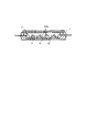
図1に本発明による第一の実施例の断面、図2にその製造工程を示す。
【0013】
パッケージ1はガラスと概ね同等の熱膨張率を有する金属板、望ましくはSUS430を公知のプレス技術により二段以上の凹部1aを有するように絞り加工したものである。ここで、最下段の凹部は信号処理IC6および抵抗、コンデンサなどの受動部品7を収納出来る容積を有し、かつ固体撮像素子5の一辺より小さい開口寸法を持つように設定されている。上段の凹部は固体撮像素子5を収納し、かつカバーガラス3がその開口を塞ぐように設定されている。
【0014】
フレキシブルプリント板(以下FPCと略す)2はポリイミドフィルム2c、回路パターンを形成した銅箔2a、さらにポリイミドのカバーフィルム2bを積層したもので、環状部21がカバーガラス3とパッケージ1との間に挟まれるように接着されており、パッケージ内の気密性を確保している。
【0015】
FPC2の一部は前記パッケージの凹部1aの内面に接着固定されている。別の一部はパッケージ外部に延在して、機器の回路(不図示)との電気的接続を行う。
【0016】
カバーガラス3は板ガラスのほか、反射防止膜、ダイクロイックフィルターなどを真空蒸着その他の方法により片面又は両面に形成した板ガラス、赤外線吸収ガラス、もしくはニオブ酸リチウム、水晶などの複屈折特性を持つ透明体が必要に応じて選択できる。さらにはこれらを積層した複合部品でもよい。
【0017】
次に、このマルチチップパッケージの製造工程を説明する。
【0018】
まず、予め絞り加工を施したパッケージ1にFPC2の環状部21及びその他の部分を接着する。ポリイミドフィルム2cにシート状接着剤(不図示)を貼付しておき、加熱加圧することで固定することが望ましい。
【0019】
その後、下段の凹部1a内のFPC2上に受動部品7を半田10bにより接続、信号処理IC6を半田付けやワイヤボンディングなど公知の技術を用いて接続する。
【0020】
必要に応じて電気的試験を行った後、上段凹部に固体撮像素子5を接着及びワイヤボンディング接続する。
【0021】
ワイヤボンディング工程で用いるワイヤ10aは概ね直径数十マイクロメートルの金属細線で、金またはアルミニウムのいずれでもよい。
【0022】
次にカバーガラス3をFPC環状部21上に接着剤4により固定し、パッケージ内部を気密封止する。ここで用いる接着剤4は気密性、非透湿性、作業性に優れていることが必要で、紫外線、及び/又は、熱によって硬化する液状接着剤が適当である。
【0023】
上述のように、本発明によれば固体撮像素子とその周辺回路素子を立体的に配置することができ、機器の小型化に好適なマルチチップパッケージを構成できる。
【0024】
(実施例2)
図3に第二の実施例を示す。
【0025】
凹部1aは概ね一段であり、その中に数点の凸部1bがプレス加工により同時に形成されている。固体撮像素子5は凸部1bに接着固定するため、より精密な寸法精度が達成できる。
【0026】
また、信号処理IC6をバンプ10cによりFPC2にフリップチップ接続すると、パッケージ全体の厚さをより薄くすることが可能である。バンプ10cの材質は半田、金などが用いられる。
【0027】
言うまでもないが、パッケージ1の絞り形状と信号処理IC6の接続方法とは上記の組合せに限る必要はなく、適宜変更することが可能である。
【0028】
(実施例3)
図4に第三の実施例を示す。
【0029】パッケージ1は前述のごとく板金であるため、孔1cや折り曲げ部1dなどを容易かつ高精度に加工できる。
【0030】したがって、このマルチチップパッケージを不図示の機器筐体に組み立てる場合、位置決め及び固定が簡易になり、機器の組立作業を大幅に簡略化できる。また、機器側にFPC2と嵌合するコネクタを用意すれば、半田付け作業も不要となるなど多大の効果がある。
【0031】
【発明の効果】
以上述べたように、本発明によれば安価かつ小型、高精度な固体撮像素子の実装が可能となる。
【図面の簡単な説明】
【図1】本発明の第一の実施例を示す断面図。
【図2】本発明の第一の実施例の製造工程を表す斜視図。
【図3】本発明の第二の実施例を示す断面図。
【図4】本発明の第三の実施例を示す斜視図。
【図5】従来の実施例を示す断面図。
【図6】他の従来の実施例を示す断面図。
【符号の説明】
1 パッケージ
1a 凹部
1b 凸部
1c 孔
1d 折り曲げ部
2 フレキシブルプリント板(FPC)
3 ガラス蓋
4 接着剤
5 固体撮像素子
6 信号処理IC
7 受動部品
10a ワイヤ
10b 半田
10c バンプ
21 環状部
【発明の属する技術分野】
本発明はCCD、CMOSなどの固体撮像素と周辺回路部品とを一体に実装するマルチチップパッケージに関するものである。
【0002】
【従来の技術】
近年、デジタルビデオカメラ、デジタルスチルカメラなど映像・画像の入力機器(以下、機器と略す)、が急速に普及している。そして、これらの機器ではより高機能化、小型化と低価格化が並行して求められ、固体撮像素子を機器へ搭載するための実装方法にも一層の小型化、低価格化が求められている。
【0003】
そのような課題を解決する目的で、固体撮像素子のみならず、その周辺に実装すべき素子も一体化するマルチチップパッケージが多く提案されている。
【0004】
例えば図5に示す特開平10−084509号公報(松下電子工業株式会社)では、セラミックパッケージの内部に固体撮像素子及び周辺回路素子を搭載した基板を収納し、ガラスなどの蓋で封止する技術が開示されている。
【0005】
また、図6の特開平11−261044号公報(松下電器産業株式会社)では、基板に周辺回路素子をフリップチップ実装し、その裏面に固体撮像素子を接着した後、周囲を封止する技術が開示されている。
【0006】
しかしながら、上記の技術には以下のごとき欠点がある。
【0007】
すなわち、特開平10−084509号公報では固体撮像素子と周辺回路素子とを平面的に配置するため、高価な部品であるセラミックパッケージとガラス蓋の大型化を招き、低コスト化の要請を十分に満足することが出来ない。
【0008】
また、特開平11−261044号公報では、周辺回路素子と固体撮像素子同士を積重ねることで実装面積は小さくなるものの、両者がほぼ同等の平面寸法を有することが必要で設計上著しい制約となる。
【0009】
さらには一方の素子の発熱が他方に伝導しやすく、温度変化に敏感な固体撮像素子には適さないという欠点もある。
【0010】
【発明が解決しようとする課題】
本発明は上記の問題に鑑みてなされたもので、固体撮像素子とその周辺回路素子を低価格かつ小型に一体封止するマルチチップパッケージを提供するものである。
【0011】
【課題を解決するための手段】
上記課題を達成する手段として、本発明では安価なプレス板金とフレキシブルプリント板、さらにガラス板を接着により組合せ、各種素子の積重ね実装を小型かつ容易に行えるようにしたものである。
【0012】
【発明の実施の形態】
(実施例1)
図1に本発明による第一の実施例の断面、図2にその製造工程を示す。
【0013】
パッケージ1はガラスと概ね同等の熱膨張率を有する金属板、望ましくはSUS430を公知のプレス技術により二段以上の凹部1aを有するように絞り加工したものである。ここで、最下段の凹部は信号処理IC6および抵抗、コンデンサなどの受動部品7を収納出来る容積を有し、かつ固体撮像素子5の一辺より小さい開口寸法を持つように設定されている。上段の凹部は固体撮像素子5を収納し、かつカバーガラス3がその開口を塞ぐように設定されている。
【0014】
フレキシブルプリント板(以下FPCと略す)2はポリイミドフィルム2c、回路パターンを形成した銅箔2a、さらにポリイミドのカバーフィルム2bを積層したもので、環状部21がカバーガラス3とパッケージ1との間に挟まれるように接着されており、パッケージ内の気密性を確保している。
【0015】
FPC2の一部は前記パッケージの凹部1aの内面に接着固定されている。別の一部はパッケージ外部に延在して、機器の回路(不図示)との電気的接続を行う。
【0016】
カバーガラス3は板ガラスのほか、反射防止膜、ダイクロイックフィルターなどを真空蒸着その他の方法により片面又は両面に形成した板ガラス、赤外線吸収ガラス、もしくはニオブ酸リチウム、水晶などの複屈折特性を持つ透明体が必要に応じて選択できる。さらにはこれらを積層した複合部品でもよい。
【0017】
次に、このマルチチップパッケージの製造工程を説明する。
【0018】
まず、予め絞り加工を施したパッケージ1にFPC2の環状部21及びその他の部分を接着する。ポリイミドフィルム2cにシート状接着剤(不図示)を貼付しておき、加熱加圧することで固定することが望ましい。
【0019】
その後、下段の凹部1a内のFPC2上に受動部品7を半田10bにより接続、信号処理IC6を半田付けやワイヤボンディングなど公知の技術を用いて接続する。
【0020】
必要に応じて電気的試験を行った後、上段凹部に固体撮像素子5を接着及びワイヤボンディング接続する。
【0021】
ワイヤボンディング工程で用いるワイヤ10aは概ね直径数十マイクロメートルの金属細線で、金またはアルミニウムのいずれでもよい。
【0022】
次にカバーガラス3をFPC環状部21上に接着剤4により固定し、パッケージ内部を気密封止する。ここで用いる接着剤4は気密性、非透湿性、作業性に優れていることが必要で、紫外線、及び/又は、熱によって硬化する液状接着剤が適当である。
【0023】
上述のように、本発明によれば固体撮像素子とその周辺回路素子を立体的に配置することができ、機器の小型化に好適なマルチチップパッケージを構成できる。
【0024】
(実施例2)
図3に第二の実施例を示す。
【0025】
凹部1aは概ね一段であり、その中に数点の凸部1bがプレス加工により同時に形成されている。固体撮像素子5は凸部1bに接着固定するため、より精密な寸法精度が達成できる。
【0026】
また、信号処理IC6をバンプ10cによりFPC2にフリップチップ接続すると、パッケージ全体の厚さをより薄くすることが可能である。バンプ10cの材質は半田、金などが用いられる。
【0027】
言うまでもないが、パッケージ1の絞り形状と信号処理IC6の接続方法とは上記の組合せに限る必要はなく、適宜変更することが可能である。
【0028】
(実施例3)
図4に第三の実施例を示す。
【0029】パッケージ1は前述のごとく板金であるため、孔1cや折り曲げ部1dなどを容易かつ高精度に加工できる。
【0030】したがって、このマルチチップパッケージを不図示の機器筐体に組み立てる場合、位置決め及び固定が簡易になり、機器の組立作業を大幅に簡略化できる。また、機器側にFPC2と嵌合するコネクタを用意すれば、半田付け作業も不要となるなど多大の効果がある。
【0031】
【発明の効果】
以上述べたように、本発明によれば安価かつ小型、高精度な固体撮像素子の実装が可能となる。
【図面の簡単な説明】
【図1】本発明の第一の実施例を示す断面図。
【図2】本発明の第一の実施例の製造工程を表す斜視図。
【図3】本発明の第二の実施例を示す断面図。
【図4】本発明の第三の実施例を示す斜視図。
【図5】従来の実施例を示す断面図。
【図6】他の従来の実施例を示す断面図。
【符号の説明】
1 パッケージ
1a 凹部
1b 凸部
1c 孔
1d 折り曲げ部
2 フレキシブルプリント板(FPC)
3 ガラス蓋
4 接着剤
5 固体撮像素子
6 信号処理IC
7 受動部品
10a ワイヤ
10b 半田
10c バンプ
21 環状部
Claims (9)
- 固体撮像素子チップとその周辺回路チップ、増幅器、抵抗、コンデンサなどを一体に封止したマルチチップパッケージであって、
前記固体撮像素子チップ、周辺回路チップ、増幅器、抵抗、コンデンサなどは少なくとも一枚のフレキシブルプリント板に固定、配線接続されており、
このフレキシブルプリント板は少なくとも一段以上の凹部を持つパッケージの内面に沿って一部又は全部が固定されており、かつ、
パッケージの凹部を密閉する透光性基板と、パッケージとの間隙からパッケージ外部に向けて延在していることを特長とするマルチチップパッケージ。 - 前記周辺回路チップ、増幅器、抵抗、コンデンサなどの内、少なくとも一つ以上は前記固体撮像素子チップと前記パッケージに挟まれた領域に配置されていることを特長とする請求項1のマルチチップパッケージ。
- 前記フレキシブルプリント板の、前記パッケージと前記透光性基板との間に挟まれる部分は、環状に形成されていることを特長とする請求項1のマルチチップパッケージ。
- 前記パッケージは絞り加工、曲げ加工、孔明け加工、エッチング加工、等を施した金属板であることを特長とする請求項1のマルチチップパッケージ。
- 前記金属板はSUS430、42アロイ、パーマロイ、コバール、フェライト、インバー、スーパーインバー、モリブデンなどの低熱膨張金属であることを特長とする請求項1のマルチチップパッケージ。
- 前記パッケージには取付け、及び/又は、位置決め用の折り曲げ部、嵌合孔、ネジ孔、長孔、切り欠き部、溝等が設けられていることを特長とする請求項1のマルチチップパッケージ。
- 前記フレキシブルプリント板の環状部およびその他の部分と、前記パッケージとは接着剤で固定されていることを特長とする請求項1のマルチチップパッケージ。
- 前記フレキシブルプリント板の環状部と、前記透光性基板とは紫外線及び/又は熱により硬化する接着剤で固定されていることを特長とする請求項1のマルチチップパッケージ。
- 前記透光性基板は、ガラス、赤外線吸収ガラス、ダイクロイックフィルター、ニオブ酸リチウム板、水晶板等などのうち一種類以上を組み合わせた積層板であることを特長とする請求項1のマルチチップパッケージ。
Priority Applications (1)
| Application Number | Priority Date | Filing Date | Title |
|---|---|---|---|
| JP2003125322A JP2004335533A (ja) | 2003-04-30 | 2003-04-30 | マルチチップパッケージ |
Applications Claiming Priority (1)
| Application Number | Priority Date | Filing Date | Title |
|---|---|---|---|
| JP2003125322A JP2004335533A (ja) | 2003-04-30 | 2003-04-30 | マルチチップパッケージ |
Publications (1)
| Publication Number | Publication Date |
|---|---|
| JP2004335533A true JP2004335533A (ja) | 2004-11-25 |
Family
ID=33502624
Family Applications (1)
| Application Number | Title | Priority Date | Filing Date |
|---|---|---|---|
| JP2003125322A Withdrawn JP2004335533A (ja) | 2003-04-30 | 2003-04-30 | マルチチップパッケージ |
Country Status (1)
| Country | Link |
|---|---|
| JP (1) | JP2004335533A (ja) |
Cited By (8)
| Publication number | Priority date | Publication date | Assignee | Title |
|---|---|---|---|---|
| WO2011078350A1 (ja) | 2009-12-24 | 2011-06-30 | 京セラ株式会社 | 撮像装置 |
| JP2012009547A (ja) * | 2010-06-23 | 2012-01-12 | Sony Corp | 固体撮像装置、電子機器 |
| JP2013077739A (ja) * | 2011-09-30 | 2013-04-25 | Kyocera Corp | 配線基板ならびにその配線基板を備えた電子装置および電子モジュール装置 |
| KR20150007667A (ko) * | 2013-07-12 | 2015-01-21 | 엘지이노텍 주식회사 | 카메라 모듈 |
| JP2015177310A (ja) * | 2014-03-14 | 2015-10-05 | 株式会社東芝 | カメラモジュール |
| WO2016042819A1 (ja) * | 2014-09-19 | 2016-03-24 | 京セラ株式会社 | 電子素子実装用基板および電子装置 |
| JP2019102582A (ja) * | 2017-11-30 | 2019-06-24 | 日亜化学工業株式会社 | 発光装置 |
| WO2019188026A1 (ja) * | 2018-03-30 | 2019-10-03 | ソニーセミコンダクタソリューションズ株式会社 | 固体撮像装置、固体撮像装置の製造方法、及び固体撮像装置を搭載した電子機器 |
-
2003
- 2003-04-30 JP JP2003125322A patent/JP2004335533A/ja not_active Withdrawn
Cited By (14)
| Publication number | Priority date | Publication date | Assignee | Title |
|---|---|---|---|---|
| US8866067B2 (en) | 2009-12-24 | 2014-10-21 | Kyocera Corporation | Imaging device with an imaging element and an electronic component |
| WO2011078350A1 (ja) | 2009-12-24 | 2011-06-30 | 京セラ株式会社 | 撮像装置 |
| JP2012009547A (ja) * | 2010-06-23 | 2012-01-12 | Sony Corp | 固体撮像装置、電子機器 |
| JP2013077739A (ja) * | 2011-09-30 | 2013-04-25 | Kyocera Corp | 配線基板ならびにその配線基板を備えた電子装置および電子モジュール装置 |
| KR102072428B1 (ko) * | 2013-07-12 | 2020-03-02 | 엘지이노텍 주식회사 | 카메라 모듈 |
| KR20150007667A (ko) * | 2013-07-12 | 2015-01-21 | 엘지이노텍 주식회사 | 카메라 모듈 |
| JP2015177310A (ja) * | 2014-03-14 | 2015-10-05 | 株式会社東芝 | カメラモジュール |
| WO2016042819A1 (ja) * | 2014-09-19 | 2016-03-24 | 京セラ株式会社 | 電子素子実装用基板および電子装置 |
| JPWO2016042819A1 (ja) * | 2014-09-19 | 2017-06-29 | 京セラ株式会社 | 電子素子実装用基板および電子装置 |
| CN106471620B (zh) * | 2014-09-19 | 2019-10-11 | 京瓷株式会社 | 电子元件安装用基板及电子装置 |
| CN106471620A (zh) * | 2014-09-19 | 2017-03-01 | 京瓷株式会社 | 电子元件安装用基板及电子装置 |
| JP2019102582A (ja) * | 2017-11-30 | 2019-06-24 | 日亜化学工業株式会社 | 発光装置 |
| WO2019188026A1 (ja) * | 2018-03-30 | 2019-10-03 | ソニーセミコンダクタソリューションズ株式会社 | 固体撮像装置、固体撮像装置の製造方法、及び固体撮像装置を搭載した電子機器 |
| US11563049B2 (en) | 2018-03-30 | 2023-01-24 | Sony Semiconductor Solutions Corporation | Solid-state imaging apparatus, method for manufacturing solid-state imaging apparatus, and electronic equipment equipped with solid-state imaging apparatus |
Similar Documents
| Publication | Publication Date | Title |
|---|---|---|
| JP3738824B2 (ja) | 光学装置及びその製造方法並びに電子機器 | |
| US20050189622A1 (en) | Packaged acoustic and electromagnetic transducer chips | |
| JP5197421B2 (ja) | カメラモジュール | |
| US7755694B2 (en) | Image sensor package and image capture device with same | |
| JP2007208045A (ja) | 撮像装置、カメラモジュール、電子機器および撮像装置の製造方法 | |
| JP2004242166A (ja) | 光モジュール及びその製造方法並びに電子機器 | |
| JP2008263550A (ja) | 固体撮像装置およびその製造方法 | |
| US20140204461A1 (en) | Optical device storage package, optical filter device, optical module, and electronic apparatus | |
| JP3867785B2 (ja) | 光モジュール | |
| JP2004335533A (ja) | マルチチップパッケージ | |
| JP2003168793A (ja) | 固体撮像装置およびその製造方法 | |
| JP2009111334A (ja) | 光学デバイスおよびその製造方法、並びに半導体デバイス | |
| WO2020062140A1 (zh) | 芯片封装结构、方法和电子设备 | |
| JP4361300B2 (ja) | 光モジュール及びその製造方法並びに電子機器 | |
| JPH04235475A (ja) | 固体撮像装置 | |
| JP4145619B2 (ja) | 光モジュール及びその製造方法、回路基板並びに電子機器 | |
| JP4292383B2 (ja) | 光デバイスの製造方法 | |
| JP3748799B2 (ja) | 電子部品パッケージ及びその実装方法 | |
| JPH09199701A (ja) | 固体撮像装置 | |
| JP2010220245A (ja) | 撮像装置、カメラモジュール、電子機器および撮像装置の製造方法 | |
| JP4138436B2 (ja) | 光モジュール、回路基板及び電子機器 | |
| JP2008263551A (ja) | 固体撮像装置およびその製造方法 | |
| JP2008166521A (ja) | 固体撮像装置 | |
| JP2007158184A (ja) | 固体撮像装置 | |
| JP2005210409A (ja) | カメラモジュール |
Legal Events
| Date | Code | Title | Description |
|---|---|---|---|
| A300 | Application deemed to be withdrawn because no request for examination was validly filed |
Free format text: JAPANESE INTERMEDIATE CODE: A300 Effective date: 20060704 |