【0001】
【発明の属する技術分野】
本発明は、プラズマディスプレイ等に用いることが可能な電磁波および赤外線を遮蔽する光学フィルタに関するものである。
【0002】
【従来の技術】
従来より、直接人が接近して利用する電磁波を発生する電子装置、例えばプラズマディスプレイ等のディスプレイ用電子管は、人体への影響を考慮して、電磁波放出の強さを規格内に抑えることが要求されている。これらの要求に対応するため、一般には、電磁波を発生する電子装置等の外部へ流出する電磁波を除去ないし減衰させるために、電磁波シールド等が用いられており、プラズマディスプレイパネル(以下、PDPともいう。)等のディスプレイ用パネルでは、良好な透視性の光学フィルタを前面に設けるのが普通である。
【0003】
これらの電磁波を遮蔽する方法としては、銀等の金属をスパッタリングにより積層する方法や、金属薄膜からなるメッシュを透明基材上に積層して用いる方法(例えば特許文献1)等が知られている。
【0004】
また、光学フィルタには、他の機器の誤動作の防止やリモートコントロールの操作性のため、ディスプレイ内部から発生する近赤外線をカットまたは吸収する機能が求められており、一般的には赤外線吸収フィルム等を積層する方法が用いられている。ここで、上記金属薄膜からなるメッシュと、赤外線吸収フィルム等を積層した場合には、上記メッシュの凹凸によって貼りあわせの際に、気泡を噛みこんでしまうこと等によって、透明性が劣ることから、オートクレーブ中の減圧環境下にて、一定時間放置する等の脱泡処理等を行う必要があり、製造効率やコストの面で問題があった。
【0005】
このような問題を解決するために、上記メッシュの凹凸を平坦化するために設けられる平坦化層や、上記金属メッシュと透明基材とを接着する接着層等に、赤外線吸収機能を有する赤外線吸収剤を添加する方法等が報告されている(特許文献1および特許文献2)。しかしながら、上記平坦化層や上記接着層等に上記赤外線吸収剤を含有させた場合には、その層を構成する樹脂の種類等によっては、上記赤外線吸収剤が反応してしまう等の問題があり、赤外線吸収の機能を十分に発揮できない場合がある等の問題があった。
【0006】
【特許文献1】
特開2002−311843号公報
【特許文献2】
特開2000−59083号公報
【0007】
【発明が解決しようとする課題】
そこで、製造が容易であり、かつ電磁波および赤外線を安定して遮蔽する光学フィルタの提供が望まれている。
【0008】
【課題を解決するための手段】
本発明は、透明基材と、上記透明基材上に形成された接着層と、上記接着層上に形成された金属メッシュとを有する電磁波遮蔽用基板、および上記電磁波遮蔽用基板上に形成され、かつ水酸基価が10以下である透明樹脂に赤外線を吸収する赤外線吸収剤が含有された赤外線吸収剤含有層を有することを特徴とする光学フィルタを提供する。
【0009】
本発明によれば、電磁波遮蔽性を有する電磁波遮蔽用基板上に形成された、赤外線吸収剤含有層中に赤外線吸収剤が含有されることから、別途赤外線吸収用フィルム等を貼りあわせる工程が必要なく、電磁波遮蔽性および赤外線吸収性を有する、製造効率やコストの面からも好ましい光学フィルタとすることができるのである。また、上記赤外線吸収剤含有層に用いられる透明樹脂の水酸基価が、上記範囲内であることにより、その透明樹脂に含有される赤外線吸収剤と、透明樹脂が有する水酸基とが反応等することを防ぐことができ、安定に赤外線吸収の機能を発揮することが可能な光学フィルタとすることができる。
【0010】
さらに本発明においては、上記透明樹脂の酸価が10以下であることが好ましい。これにより、上記透明樹脂中に含有される赤外線吸収剤が、透明樹脂中の酸と反応することを防ぐことも可能となり、より安定に赤外線吸収の機能を発揮することが可能な光学フィルタとすることができるからである。
【0011】
また、本発明においては、上記透明樹脂の、ガラス転移温度(Tg)が−80℃〜−10℃の範囲内であり、上記赤外線吸収剤含有層が粘着性を有する赤外線吸収剤含有粘着層であってもよい。これにより、赤外線吸収剤含有層を、本発明の光学フィルタと、例えばプラズマディスプレイパネル等の他の部材と接着する層として用いることが可能となるからである。
【0012】
また、上記発明においては、上記赤外線吸収剤含有層上に透明粘着層を有するものであってもよい。これにより、本発明の光学フィルタを、他の部材と貼りあわせることが可能となるからである。また上記赤外線吸収剤含有層が粘着性を有する場合であっても、例えば金属を含有するガラスからなるプラズマディスプレイパネル等の他の部材と貼りあわせる場合、上記赤外線吸収剤含有層中に含有される赤外線吸収剤が、そのガラスに含まれる金属と反応等してしまう場合があることから、上記透明粘着層を形成することにより、赤外線吸収剤と他の部材とが接触しないようにすることが可能となるからである。
【0013】
また、本発明においては、上記電磁波遮蔽用基板が、上記金属メッシュ上に形成された平坦化層を有していてもよい。これにより、上記電磁波遮蔽用基板において、上記金属メッシュの凹凸を平坦化することができ、高品質な光学フィルタとすることができるからである。
【0014】
本発明においては、上記電磁波遮蔽用基板が、上記金属メッシュの断面に形成されたメッシュ断面被覆層を有していてもよい。これにより、金属メッシュ断面の乱反射を防ぐことができ、さらに例えば金属メッシュ上に接着層等を設けた際、メッシュ空隙部分の底部の隅に気泡が入ることを防ぐことができるからである。
【0015】
さらに、本発明においては、上記金属メッシュの空隙部分が、上記接着層により充填されているものであってもよい。これにより、平坦化層等を用いることなく上記金属メッシュの凹凸を平坦化することができ、高品質な光学フィルタとすることができるからである。
【0016】
また、本発明の光学フィルタは、補強材を有していてもよい。これにより、強度を有する光学フィルタとすることができるからである。
【0017】
さらに、本発明の光学フィルタは、反射防止層を有していてもよい。これにより、上記電磁波遮蔽および赤外線吸収の機能だけでなく、可視光等の反射防止の機能も有する光学フィルタとすることができるからである。
【0018】
また、本発明の光学フィルタは、ネオン光吸収層を有していてもよい。これにより、例えばプラズマディスプレイパネル等の色調を調整することが可能な光学フィルタとすることができるからである。
【0019】
【発明の実施の形態】
本発明は、製造が容易であり、かつ電磁波および赤外線を安定して遮蔽する光学フィルタに関するものである。以下、本発明の光学フィルタについて説明する。
【0020】
本発明の光学フィルタは、透明基材と、上記透明基材上に形成された接着層と、上記接着層上に形成された金属メッシュとを有する電磁波遮蔽用基板、および上記電磁波遮蔽用基板上に形成され、かつ水酸基価が10以下である透明樹脂に赤外線を吸収する赤外線吸収剤が含有された赤外線吸収剤含有層を有することを特徴とするものである。
【0021】
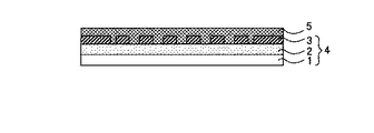
本発明の光学フィルタは、例えば図1に示すように、透明基材1と、その透明基材1上に形成された接着層2と、その接着層2上に形成された金属メッシュ3とを有する電磁波遮蔽用基板4と、その電磁波遮蔽用基板4上に形成された赤外線吸収剤含有層5とを有するものである。
【0022】
本発明によれば、電磁波遮蔽の機能を有する電磁波遮蔽用基板上に、上記赤外線吸収剤を含有する赤外線吸収剤含有層が形成されることから、別途赤外線吸収フィルムを貼りあわせる必要がなく、電磁波遮蔽の機能および赤外線吸収の機能を有する、製造効率やコストの面から好ましい光学フィルタとすることができる。
【0023】
また通常、透明樹脂の中に赤外線吸収剤を含有する場合において、その透明樹脂が水酸基を有する場合には、その水酸基により例えば対イオンを有する赤外線吸収剤が反応等する場合がある。本発明においては、上記赤外線吸収剤含有層に用いられる透明樹脂の水酸基価が上記範囲内であることから、その透明樹脂中に含有される赤外線吸収剤が透明樹脂中の水酸基と反応等することを防止することができ、安定に赤外線吸収の機能を発揮することが可能な光学フィルタとすることができるのである。
【0024】
ここで、本発明の光学フィルタには、2つの実施態様があり、第1実施態様としては、上記赤外線吸収剤含有層が粘着性を有する赤外線吸収剤含有粘着層である場合であり、第2実施態様としては、上記赤外線吸収剤含有層が粘着性を有しない赤外線吸収剤含有コーティング層である場合である。
【0025】
以下、本発明の光学フィルタの各実施態様ごとにわけて説明する。
【0026】
A.第1実施態様
まず、本発明の光学フィルタにおける第1実施態様について説明する。本発明の光学フィルタにおける第1実施態様は、透明基材と、上記透明基材上に形成された接着層と、上記接着層上に形成された金属メッシュとを有する電磁波遮蔽用基板、および上記電磁波遮蔽用基板上に形成され、かつ水酸基価が10以下である透明樹脂に赤外線を吸収する赤外線吸収剤が含有された赤外線吸収剤含有層を有するものであり、かつ上記赤外線吸収剤含有層は、用いられる透明樹脂のガラス転移温度(Tg)が所定の範囲内であり、粘着性を有する赤外線吸収剤含有粘着層であることを特徴とするものである。
【0027】
本実施態様によれば、上記赤外線吸収剤含有層が粘着性を有する赤外線吸収剤含有粘着層であることから、本実施態様の光学フィルタと、例えばプラズマディスプレイパネル等の他の部材とを赤外線吸収剤含有粘着層によって接着することが可能となるのである。
【0028】
以下、本実施態様における光学フィルタの各構成について説明する。
【0029】
1.赤外線吸収剤含有粘着層
まず、本実施態様に用いられる赤外線吸収剤含有粘着層について説明する。本実施態様に用いられる赤外線吸収剤含有粘着層は、後述する電磁波遮蔽用基板上に形成される層であって、水酸基価が10以下である透明樹脂に赤外線を吸収する赤外線吸収剤が含有された層であり、さらに上記透明樹脂が、ガラス転移温度(Tg)が所定の値以下であって粘着性を有する層である。本実施態様の光学フィルタにおいて、この赤外線吸収剤含有粘着層は、例えばプラズマディスプレイ等から発せられた赤外線を吸収する機能を果たすものである。また例えばプラズマディスプレイパネルや補強剤等の他の部材と、本実施態様の光学フィルタとを接着する層としての機能を果たすものである。以下、このような赤外線吸収剤含有粘着層の各構成について説明する。
【0030】
(透明樹脂)
まず、本実施態様の赤外線吸収剤含有粘着層に用いられる透明樹脂について説明する。本実施態様の赤外線吸収剤含有粘着層に用いられる透明樹脂としては、可視光に対して透過率の高い樹脂であり、かつ水酸基価およびガラス転移点温度(Tg)が所定の値以下のものであって粘着性を有するものである。
【0031】
本実施態様において、このような透明樹脂の水酸基価は、10以下、中でも5以下、特に、0であることが好ましい。これにより、透明樹脂中に含有される、例えば対イオンを有する赤外線吸収剤が、透明樹脂に含まれる水酸基により反応すること等を防ぐことができ、安定に赤外線吸収の機能を有する光学フィルタとすることが可能となる。また赤外線吸収剤の選択の幅を広げることも可能となる。ここで、水酸基価とは、試料1gをアセチル化するとき、水酸基と結合した酢酸を中和するのに要する水酸化カリウムのmg量をいうものである。
【0032】
また、本実施態様において、透明樹脂のガラス転移点温度は、−80℃〜−10℃の範囲内、中でも−60℃〜−20℃の範囲内であることが好ましい。これにより、本実施態様に用いられる赤外線吸収剤含有粘着層に粘着性を付与することが可能となり、本発明の光学フィルタを、例えばプラズマディスプレイ用パネル等の他の部材に接着することが可能となるからである。
【0033】
また、本実施態様においては、上記透明樹脂の酸価が、10以下、中でも5以下、特に、0であることが好ましい。これにより、透明樹脂中に含有される酸により、赤外線吸収剤が反応すること等を防ぐことができ、さらに安定に赤外線吸収の機能を発揮する光学フィルタとすることができるからである。ここで、酸価とは、試料1gを中和するのに要する水酸化カリウムのmg量をいう。
【0034】
本実施態様に用いられる、上述したような性質を有する材料として、具体的には、アクリル系樹脂、エステル系樹脂、ウレタン系樹脂、エポキシ系樹脂、ポリウレタンエステル系樹脂、またはポリテトラフルオロエチレン(PTFE)、テトラフルオロエチレンとペルフルオロアルキルビニルエ−テルとの共重合体からなるペルフルオロアルコキシ樹脂(PFA)、テトラフルオロエチレンとヘキサフルオロプロピレンコポリマ−(FEP)、テトラフルオロエチレンとペルフルオロアルキルビニルエ−テルとヘキサフルオロプロピレンコポリマ−(EPE)、テトラフルオロエチレンとエチレンまたはプロピレンとのコポリマ−(ETFE)、ポリクロロトリフルオロエチレン樹脂(PCTFE)、エチレンとクロロトリフルオロエチレンとのコポリマ−(ECTFE)、フッ化ビニリデン系樹脂(PVDF)、フッ化ビニル系樹脂(PVF)等のフッ素系樹脂、ポリイミド、ポリアミドイミド、ポリエーテルイミド等のポリイミド系樹脂、シリコーン系樹脂等を挙げることができ、中でもアクリル系樹脂、エステル系樹脂、ポリカーボネート系樹脂であることが好ましい。
【0035】
また、上記樹脂の平均分子量は、500〜120万の範囲内、中でも20万〜100万であることが好ましい。これにより、上記のような性質を有する透明樹脂とすることができるからである。
【0036】
本実施態様においては、上述した材料の中でも、アクリル系樹脂であることが好ましく、中でも2−エチルヘキシル(2HA)、ブチルアクリレート(BA)を主成分として用いることが好ましい。
【0037】
(赤外線吸収剤)
次に、赤外線吸収剤含有粘着層に用いられる赤外線吸収剤について説明する。本実施態様に用いられる赤外線吸収剤は、赤外領域の光を吸収する材料であれば、その種類等は特に限定されるものではない。一般に赤外領域とは800〜1200nmの領域を示し、本実施態様に用いられる赤外線吸収剤においては、上記領域内での光の透過率が20%以下、中でも10%以下であることが好ましい。上記透過率は、分光光度計 UV−3100PC 島津製作所製にてJIS Z8722「色の測定方法−反射及び透過物体色」に記載される方法にて測定を行った値である。
【0038】
本実施態様において、赤外線吸収剤として、具体的には、酸化スズ、酸化インジウム、酸化マグネシウム、酸化チタン、酸化クロム、酸化ジルコニウム、酸化ニッケル、酸化アルミニウム、酸化亜鉛、酸化鉄、酸化アンチモン、酸化鉛、酸化ビスマス等の無機赤外線吸収剤、シアニン系化合物、フタロシアニン系化合物、ナフタロシアニン系化合物、ナフトキノン系化合物、アントラキノン系化合物、アルミニウム系化合物、ピリリウム系化合物、セリリウム系化合物、スクワリリウム系化合物、ジイモニウム類、銅錯体類、ニッケル錯体類、ジチオール系錯体類等の有機赤外線吸収剤を1種類、または2種類以上混合して用いることができる。
【0039】
また、上記の有機赤外線吸収剤として具体的には、(以下、日本化薬社製:商品名)IRG−002、IRG−003、IRG−022、IRG−023、IRG−040、(以下、日本触媒社製:商品名)IR−1、IR−10、IR−12、IR−14、TX−EX−906B、TX−EX−910B、(以下、三井化学ファイン社製:商品名)SIR−128、SIR−130、SIR−132、SIR−159、(以下、みどり化学社製:商品名)MIR−101、MIR−111、MIR−121、MIR−102、MIR−1011、MIR−1021等が挙げられる。
【0040】
通常、対イオン構造の赤外線吸収剤を用いた場合には、その赤外線吸収剤が含有される透明樹脂が水酸基やカルボキシル基、重合開始剤等を有する場合には、その水酸基やカルボキシル基、重合開始剤等により対イオンの均衡状態が崩れ、赤外線吸収の機能を果たすことが困難となる場合がある。
【0041】
本実施態様においては、上述した透明樹脂を用いることから、対イオン構造の赤外線吸収剤であっても、反応等することがなく、本実施態様の効果をより発揮することができるという面から、上記の中でも対イオン構造を有するジイモニウム類、ニッケル錯体類、ジチオール系錯体類、アルミニウム系化合物、シアニン系化合物、ピリリウム系化合物であることが好ましい。
【0042】
また、本実施態様によれば、上記透明樹脂中に上記赤外線吸収剤を含有させる方法としては、上記透明樹脂を溶融させた中に、上記赤外線吸収剤を加え、溶融混練等を行う方法であってもよく、また上記赤外線吸収剤を溶剤等に溶解させて、上記透明樹脂中に混合する方法であってもよい。本実施態様によれば、上述した透明樹脂を用いることから、どちらの方法においても上記赤外線吸収剤を安定に分散させることが可能となるのである。
【0043】
ここで、本実施態様において、上記のうち無機赤外線吸収剤は、微粒子であることが好ましく、平均粒径は0.01μm〜1μmの範囲内であることが好ましく、中でも0.05μm〜0.5μmの範囲内であることが好ましい。また、上記赤外線吸収剤の粒径は、可視光線透過率を良好なものとするために、1μm以下の分布であることが好ましい。
【0044】
(赤外線吸収剤含有粘着層)
次に、本実施態様に用いられる赤外線吸収剤含有粘着層について説明する。本実施態様に用いられる赤外線吸収剤含有粘着層は、上記透明樹脂中に、上記赤外線吸収剤が含有されたものであり、この赤外線吸収剤含有粘着層の膜厚が0.5μm〜50μmの範囲内、中でも5μm〜40μmであることが好ましい。これにより、後述する電磁波吸収用基板および、例えばプラズマディスプレイパネル等の他の部材とを強固に接着することができ、また赤外線吸収の機能を果たすことができるからである。
【0045】
このような赤外線吸収剤含有粘着層の形成方法としては、上述した赤外線吸収剤が含有された上述した透明樹脂を、溶剤等により溶解させ、後述する電磁波遮蔽用基板上にメイヤーバー、グラビアコート、グラビアリバースコート、キスリバースコート、3本ロールリバースコート、スリットリバースダイコート、コンマコート、ナイフコート等の各種コーティング法により塗布し、溶剤を揮発させて乾燥させる方法等が挙げられる。また、離型フィルム等の上に上記方法により塗布し、その後電磁波遮蔽用基板に貼りあわせる方法等であってもよい。
【0046】
ここで、上記透明樹脂を塗布する際に用いられる溶剤としては、酢酸エチル、トルエン、メチルエチルケトン(MEK)、キシレン、イソプロピルアルコール(IPA)、クロロホルム、テトラヒドロフラン(THF)、ジメチルホルムアミド(DMF)、アセトニトリル、トリフルオロプロパノール等が挙げられる。
【0047】
上述したような赤外線吸収剤含有粘着層は、ドライラミネーション法、またはウェットラミネーション法等により後述する電磁波遮蔽用基板と、例えばプラズマディスプレイ等の他の部材とを接着することができるのである。
【0048】
ここで、本実施態様においては赤外線の透過率が、20%以下、中でも10%以下であることが好ましい。これにより、例えばプラズマディスプレイ等から発生する赤外線をカットまたは吸収することが可能となり、他の機器の誤動作の防止等をすることができるからである。ここで、上記透過率は、上述した測定法により測定した値である。
【0049】
なお、本実施態様の赤外線吸収剤含有粘着層は、必要に応じて粘着付与剤、充填剤、軟化材、酸化防止剤、紫外線吸収剤、架橋剤等を含有するものであってもよい。
【0050】
2.電磁波遮蔽用基板
次に、本実施態様に用いられる電磁波遮蔽用基板について説明する。本実施態様に用いられる電磁波遮蔽用基板は、透明基材と、その透明基材上に形成された接着層と、その接着層上に形成された金属メッシュとを有するものであり、例えばプラズマディスプレイ等から発せられる電磁波を遮蔽することが可能な基板であれば、特に限定されるものではなく、例えばその金属メッシュが平坦化されたもの等であってもよい。
【0051】
以下、本実施態様に用いられる電磁波遮蔽用基板の各構成について説明する。
【0052】
(金属メッシュ)
まず、本実施態様に用いられる電磁波遮蔽用基板の金属メッシュについて説明する。本実施態様に用いられる金属メッシュは、プラズマディスプレイ等から発生した電磁波を遮蔽する機能を有するものである。このような金属メッシュは、後述する透明基材上に、後述する接着層により金属箔が貼りあわせられ、その金属箔がメッシュ状にエッチングされることにより形成される。
【0053】
本実施態様においては、この金属メッシュは、電磁波遮蔽性を有するものであれば、その金属の種類等は特に限定されるものではなく、例えば銅、鉄、ニッケル、クロム、アルミニウム、金、銀、ステンレス、タングステン、クロム、チタン等を用いることができる。
【0054】
本実施態様においては、上記の中でも銅が、電磁波のシールド性、エッチング処理適性や取扱い性の面から好ましい。また用いられる銅箔の種類としては、圧延銅箔、電解銅箔等が挙げられるが、特に電解銅箔であることが好ましい。これにより、厚さが10μm以下の均一性のよいものとすることができ、また黒化処理された際に、酸化クロム等との密着性を良好なものとすることができるからである。
【0055】
ここで、本実施態様においては、上記金属箔の一方の面または両面に黒化処理されていることが好ましい。黒化処理とは、酸化クロム等により金属メッシュの表面を黒化する処理であり、光学フィルタにおいて、この黒化処理面は、観察者側の面となるように配置される。この黒化処理により金属メッシュ表面に形成された酸化クロム等により、光学フィルタ表面の外光が吸収されることから、光学フィルタ表面で光が散乱することを防止することができ、良好な視認性を得ることが可能な光学フィルタとすることができるのである。このような黒化処理は、上記金属箔に黒化処理液を塗布することにより行うことができる。黒化処理の方法としては、CrO2水溶液や、無水クロム酸水溶液に酒石酸、マロン酸、クエン酸、乳酸等の異なるオキシカルボン酸化合物を添加して、6価クロムの一部を3価クロムに還元した溶液等を、ロールコート法、エアーカーテン法、静電霧化法、スクイズロールコート法、浸漬法等により塗布し、乾燥させることにより行なうことができる。なお、この黒化処理は、後述する透明基材上に、後述する接着層によって金属箔が貼りあわせられ、メッシュ状にエッチングされた後に行われるものであってもよい。
【0056】
本実施態様においては、上記黒化処理された金属箔の表面の黒濃度が0.6以上であることが好ましい。これにより、より視認性を良好なものとすることができるからである。ここで、黒濃度は、COLOR CONTROL SYSTEMのGRETAG SPM100−11((株)KIMOTO製)を用いて、観測視野角10°、観測光源D50、照明タイプとして濃度標準ANSI Tに設定し、白色キャリブレイション後に測定した値である。
【0057】
また、本実施態様においては、上記金属箔の膜厚は、1μm〜100μmの範囲内、中でも5μm〜20μmの範囲内であることが好ましい。上記範囲より膜厚が厚いと、エッチングによりパターン線幅を細かく高精細化することが困難となり、また上記範囲より薄い場合には、十分な電磁波シールド性が得られないからである。
【0058】
さらに、本実施態様においては、上記金属箔は、JIS B0601に準拠する十点平均粗さが0.5μm〜10μmの範囲内であることが好ましい。上記範囲より小さい場合には、上記黒化処理をした場合であっても、光学フィルタ表面の外光が鏡面反射することから、視認性が劣化し、また上記範囲より大きい場合には、接着層やレジスト等を塗布することが困難となるからである。
【0059】
ここで、金属箔のエッチングは、後述する透明基材上に、後述する接着層を用いて貼りあわせられた後に行われるものである。本実施態様において、このエッチングは、通常のフォトリソグラフィー法により行うことができ、例えば金属箔の表面にレジストを塗布し、乾燥した後レジストをパターン版で密着露光し、現像処理を行うことにより得ることができる。
【0060】
本実施態様に用いられる上述したような金属メッシュは、表面抵抗が10−8Ω/□〜5Ω/□の範囲内、中でも10−4Ω/□〜3Ω/□の範囲内であることが好ましい。一般的に、電磁波遮蔽性は、表面抵抗により測定することができ、この表面抵抗が低いほど、電磁波遮蔽性が良好なものということができる。ここで、上記表面抵抗の値は、表面抵抗測定装置 ロレスタ−GP (株)ダイヤインスツルメンツ製にてJIS K 7194「導電性プラスチックの4探針法による抵抗率試験方法」に記載される方法にて測定された値である。
【0061】
本実施態様においては、このエッチング処理された後の金属メッシュは、50μm□〜500μm□の範囲内、中でも100μm□〜400μm□の範囲内、特に200μm□〜300μm□の範囲内であることが好ましく、またメッシュ線幅が5μm〜20μmの範囲内であることが好ましい。メッシュ線幅が上記範囲より細い場合には、断線が起こる場合等があり、電磁波遮蔽性の面から好ましくなく、またメッシュ線幅が上記範囲より太い場合には、可視光の透過率が低く、例えばプラズマディスプレイの輝度が低くなる等という面から好ましくないからである。
【0062】
(透明基材)
次に、本実施態様に用いられる電磁波遮蔽用基板における透明基材について説明する。本実施態様に用いられる透明基材は、可視光に対して透明性を有し、かつ後述する接着層と、その接着層上に上記金属メッシュとが積層されるものである。
【0063】
本実施態様においては、この透明基材は透明性を有し、かつ接着層が形成可能であれば、その種類等は特に限定されるものではなく、例えばポリエチレンテレフタレート(PET)、ポリエチレンナフタレート(PEN)、ポリカーボネート、アクリル(PMMA)、環状ポリオレフィン、トリアセチルセルロース(TAC)、ポリエーテルサルファイド(PES)、ポリエーテルケトン等を用いることができ、中でもコストや取扱い性の面等から、PETであることが好ましい。
【0064】
また、本実施態様においては、この透明基材の膜厚が12μm〜300μmの範囲内であることが好ましい。
【0065】
(接着層)
次に、本実施態様に用いられる電磁波遮蔽板における接着層について説明する。本実施態様に用いられる接着層は、上述した金属メッシュおよび透明基材とを接着することが可能な層であれば、その種類等は特に限定されるものではないが、本実施態様においては、上記金属メッシュを構成する金属箔および透明基材を接着層により貼りあわせた後、金属箔をエッチングによりメッシュ状とすることから、接着層も耐エッチング性を有することが好ましい。
【0066】
本実施態様においては、このような接着層の材料として、具体的には、アクリル系、エステル系、ウレタン系、フッ素系、ポリイミド系、エポキシ系、ポリウレタンエステル系等が挙げられる。
【0067】
また、本実施態様に用いられる接着層は、紫外線硬化型であってもよく、また熱硬化型であってもよい。本実施態様においては、これらの接着層を用いてドライラミネーション法、ウェットラミネーション法等により上記透明基材および上記金属箔とを接着することができる。
【0068】
本実施態様においては、この接着層の膜厚が0.5μm〜50μmの範囲内であることが好ましい。これにより、上記透明基材および上記金属メッシュとを強固に接着することができ、また、金属メッシュを形成するエッチングの際に透明基材がエッチング液の影響を受けること等を防ぐことができるからである。
【0069】
(電磁波遮蔽用基板)
次に、本実施態様に用いられる電磁波遮蔽用基板について説明する。本実施態様に用いられる電磁波遮蔽用基板は、上記透明基材上に上記接着層が形成され、その接着層上に上記金属メッシュが形成されたものであれば、特に限定されるものではなく、必要に応じて上記金属メッシュ、透明基材、および接着層の他に、上記金属メッシュの表面を平坦化する層等を有するものであってもよい。本実施態様においては、上記金属メッシュの表面が平坦化されているものであることが光学フィルタの透明性や汎用性等の面から好ましい。
【0070】
ここで、上記金属メッシュを平坦化する方法としては、以下の3つの態様が挙げられる。まず、第1の態様としては、上記金属メッシュの表面を平坦化する平坦化層を形成する方法であり、第2の態様としては、上記上記金属メッシュの断面にメッシュ断面被覆層を形成し、メッシュ表面を平坦化する方法である。また第3の態様としては、上記金属メッシュの空隙部分を、上記接着層により充填することによって、金属メッシュ表面を平坦化する方法である。以下、これらの平坦化の方法について各態様ごとに説明する。
【0071】
(1)第1の態様
まず、本実施態様に用いられる電磁波遮蔽用基板における上記金属メッシュ表面の平坦化方法の第1の態様について説明する。
【0072】
本実施態様の金属メッシュの平坦化における第1の態様は、上述した金属メッシュ表面を平坦化する平坦化層を形成することにより、金属メッシュの表面を平坦化する方法である。本態様における電磁波遮蔽用基板は、例えば図2に示すように、透明基材1と、その透明基材1上に形成された接着層2と、その接着層2上に形成された金属メッシュ3と、その金属メッシュ3上に形成された平坦化層6とを有するものとなる。本態様よれば、上記金属メッシュ上に平坦化層を形成することによって、上記金属メッシュの凹凸を平坦化することができ、他の部材と貼りあわせた際等に、金属メッシュによる凹凸によって光学フィルタの透明性が低下することを防ぐことができるのである。また、上述した金属メッシュ形成の際に行われるエッチングによって、上記接着層表面が劣化し、透明性が低下した場合であっても、その接着層上に平坦化層が形成されることから、透明性を改良することができ、さらに、平坦化層により金属メッシュの断面が覆われることから、金属メッシュを斜めから見た際にも乱反射を防止することができるのである。
【0073】
このような平坦化層の材料としては、可視光に対して透明性を有する樹脂であることが好ましく、具体的には、アクリル系樹脂、エステル系樹脂、ポリカーボネート系樹脂、ウレタン系樹脂、環状ポリオレフィン系樹脂、ポリスチレン系樹脂、ポリイミド系樹脂、フッ素系樹脂等が挙げられる。
【0074】
また、上記平坦化層の形成方法は、上述した材料を溶剤等に溶解させて金属メッシュ上に塗布後、溶剤を揮発させて乾燥する。その後、表面に金属メッシュの凹凸により形成された透明樹脂の凹凸を、透明樹脂基材のTg以上の温度で例えばミラーロール等を用いて圧力をかけることにより平坦化することにより形成することができる。
【0075】
このことから、上記の樹脂は、ガラス転移点温度(Tg)が30℃〜150℃の範囲内、中でも40℃〜120℃の範囲内であることが好ましい。
【0076】
また、この平坦化層を平坦化する工程における温度および圧力は、その透明樹脂の種類により適宜選択されるものであるが、通常50℃〜170℃の範囲内であり、また圧力は線圧0.1kg/cm2〜10kg/cm2の範囲内であることが好ましい。
【0077】
本態様において、このような平坦化層の膜厚は、金属メッシュが形成されていない部分、例えば図2に示すaの膜厚が、10μm〜50μmの範囲内であることが好ましい。これにより、上記金属メッシュの凹凸を平坦化することが可能となるからである。
【0078】
(2)第2の態様
次に、本実施態様に用いられる電磁波遮蔽用基板における上記金属メッシュ表面の平坦化方法の第2の態様について説明する。
【0079】
本実施態様の金属メッシュの平坦化における第2の態様は、金属メッシュの断面にメッシュ断面被覆層を形成することにより金属メッシュの表面を平坦化する方法である。本態様における電磁波遮蔽用基板は、例えば図3に示すように、透明基材1と、その透明基材1上に形成された接着層2と、その接着層2上に形成された金属メッシュ3と、その金属メッシュ3の断面および金属メッシュ3の空隙部分の底部を被覆するメッシュ断面被覆層7層とを有するものとなる。
【0080】
通常、金属メッシュを光学フィルタに用いる場合、金属メッシュを斜めから見た際に断面が乱反射し、視野角が減少することから、金属メッシュ以上の厚みを持つ透明粘着層を貼りあわせて透明化処理を行うことが必要である。この透明粘着層を貼りあわせる際、メッシュ空隙部分の底部の隅における気泡が抜け難く、例えばオートクレーブ中等に一定時間放置し、脱泡処理を行わなければならない。本態様によれば、上記メッシュ断面被覆層を形成することにより、上記気泡が残ることがないことから、脱泡処理等が必要なく、またメッシュの断面を覆うことから、斜めから見た際のメッシュ断面の乱反射も防止することができる。さらに、上記メッシュ断面被覆層によりメッシュ空隙部が充填されていることから、このメッシュ断面被覆層が形成された金属メッシュ上に透明粘着層等を用いて他の層と貼りあわせた際に、気泡等を噛みこむことなく平坦な層を形成することができるのである。
【0081】
上記メッシュ断面被覆層を形成する材料は、可視光に対して透明な樹脂である層であれば、特に限定されるものではなく具体的には、アクリル系樹脂、エステル系樹脂、ポリカーボネート系樹脂、ウレタン系樹脂、環状ポリオレフィン系樹脂、ポリスチレン系樹脂、ポリイミド系樹脂、フッ素系樹脂、等が挙げられる。
【0082】
上記メッシュ断面被覆層の形成方法としては、上記樹脂を溶剤等に希釈し、上記金属メッシュ上に印刷用スキージ等を用いて、金属メッシュ上に樹脂が残らないように塗布することにより得ることができる。
【0083】
また、この際、溶剤に希釈された上記樹脂の粘度は100Pa・s〜10000Pa・sの範囲内であることが好ましい。これにより、上記金属メッシュ空隙部分に気泡等が残ることなく、メッシュ断面被覆層を形成することができるからである。
【0084】
(3)第3の態様
次に、本実施態様の金属メッシュの平坦化における第3の態様について説明する。本実施態様の金属メッシュの平坦化における第3の態様は、金属メッシュの空隙部分を、上記接着層により充填することにより金属メッシュ表面を平坦化する方法である。本態様における電磁波遮蔽用基板は、例えば図4に示すように、上記透明基材1と、その透明基材1上に形成された接着層2と、その接着層2上に形成された金属メッシュ3とを有するものであって、その金属メッシュ3の空隙部分が上記接着層2により充填されているものとなる。
【0085】
本態様によれば、上記接着層によって、上記金属メッシュの空隙部が充填されていることにより、上記金属メッシュの凹凸が平坦化される。さらに、上記金属メッシュの断面を接着層が覆うことから、メッシュ断面の乱反射を抑えることができるのである。
【0086】
上記接着層を、上記金属メッシュの空隙部に充填する方法としては、まず、上述したように上記透明基材上に形成された上記接着層上に金属箔を貼りあわせ、その金属箔をエッチングすることにより金属メッシュを形成する。その後、例えば離型フィルムの離型処理面等を上記金属メッシュの表面に設置した後、上記接着層のガラス転移点温度以上の熱をかけて、例えばミラーロール等により加圧することにより、上記金属メッシュが上記接着層中に押し込まれ、上記金属メッシュの空隙部に上記接着層が充填されるのである。
【0087】
なお、本態様により平坦化が行われる場合には、上述した接着層の材料の中でも、ガラス転移点温度(Tg)が−60℃〜180℃の範囲内、中でも40℃〜150℃の範囲内であることが好ましい。これにより、上記工程によって容易に上記金属メッシュを押し込むことが可能となるからである。
【0088】
また、この工程における温度および圧力は、その接着層の種類により適宜選択されるものであるが、通常50℃〜170℃の範囲内であり、また圧力は線圧0.1kg/cm2〜10kg/cm2の範囲内であることが好ましい。
【0089】
3.光学フィルタ
次に、本実施態様の光学フィルタについて説明する。本実施態様の光学フィルタは、上述した電磁波遮蔽用基板上に、上述した赤外線吸収剤含有粘着層が形成されているものであり、必要に応じて他の層が積層されているもの等であってもよい。
【0090】
ここで、本実施態様における光学フィルタは、視感透過率が40%以上、中でも50%以上であることが好ましい。これにより、光学フィルタを例えばプラズマディスプレイ等に用いる際に、視認性がよいものとすることができるからである。ここで、可視光とは、380nm〜780nmの範囲内の光のことをいうこととし、上記視感透過率は分光光度計 UV−3100(島津製作所)を用いてJIS Z8701 色の表現方法 XYZ表色系及びX10Y10Z10表示系 に記載される測定方法に従って測定し、JIS Z 8722 色の測定方法−反射及び透過物体色 にて算出された、380nm〜780nmの範囲内透過率を測定した値である。
【0091】
また、通常光学フィルタが用いられる際には、金属メッシュ等の電磁波遮蔽板により遮蔽された電磁波の電気を逃がすためにアースが設置される。本実施態様の光学フィルタにおいては、上記金属メッシュが観察者側に配置される場合には、通常の方法によりアースをとることが可能であるが、例えばプラズマディスプレイ用パネル側に上記金属メッシュが配置される場合には、導電粘着テープを上記金属メッシュの外周4辺に貼りあわせたり、リベット等を用いて光学フィルタの表面側にアースをとるための接点を形成すること等により、アースをとることを可能とすることができる。
【0092】
また、本実施態様の光学フィルタは、例えば図1に示すように、上記赤外線吸収剤含有粘着層5が、上記電磁波遮蔽用基板4における透明基材1側に形成されるものであってもよく、また例えば図5に示すように、上記赤外線吸収剤含有粘着層5が、上記電磁波遮蔽用基板4における金属メッシュ3側に形成されるものであってもよい。
【0093】
また、例えば図6に示すように、電磁波遮蔽用基板4と、その電磁波遮蔽用基板4上に形成された赤外線吸収剤含有粘着層5と、その赤外線吸収剤含有粘着層5上に透明粘着層8とを有するものであってもよい。上記赤外線吸収剤含有粘着層と貼りあわせられる部材に例えば青板ガラス等の金属を含有する材料が用いられる場合、上記赤外線吸収剤含有粘着層に含有される赤外線吸収剤と、その金属とが反応等してしまう可能性があり、上記透明粘着層を形成することにより、上記赤外線吸収剤と上記部材とが接触することを防ぐことが可能となるからである。また、この透明粘着層は、上述した赤外線吸収剤含有粘着層と上述した電磁波遮蔽用基板との間に形成されていてもよい。上述した赤外線吸収剤含有粘着層中の赤外線吸収剤と、電磁波遮蔽用基板における金属メッシュとが接触する場合には、これらが反応等する場合があり、この透明粘着層を形成することによって、この反応等を防止することが可能となり、より高品質な光学フィルタとすることができるからである。
【0094】
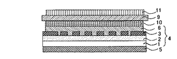
また、本実施態様においては、例えば図7に示すように、上記電磁波遮蔽用基板4上に形成された赤外線吸収剤含有粘着層5上に、補強材9を有するものであってもよい。これにより、本実施態様の光学フィルタに強度を付与することができるからである。
【0095】
さらに、本実施態様においては、例えば図8に示すように、上記電磁波遮蔽用基板4と赤外線吸収剤含有粘着層5と、その電磁波遮蔽用遮蔽用基板4側に形成されたネオン光吸収層10を有するものであってもよい。このネオン光吸収層によって、例えばプラズマディスプレイパネル等の色調を調整することが可能となり、高品質な光学フィルタとすることができるからである。
【0096】
また例えば図9に示すように、上記ネオン光吸収層10上に上記補強材9が形成され、さらにその補強材9上に反射防止層11等が形成されたもの等であってもよい。これにより、上記電磁波遮蔽および赤外線吸収の機能だけでなく、可視光等の反射防止の機能も有する光学フィルタとすることができるからである。
【0097】
なお、これらの層が積層される場合、上述したように、上記電磁波遮蔽用基板において上記金属メッシュが平坦化されていることが好ましい。これにより、上記電磁波遮蔽用基板上に層が形成される際、気泡等が噛みこまれることにより透明性が低下する等の問題が起きることがなく、製造効率よく高品質な光学フィルタとすることができるのである。また、上記のどの場合においても、上記電磁波遮蔽用基板における金属メッシュの黒化処理面は、光学フィルタとして用いられた際に、観察者側となるように形成される。
【0098】
ここで、本実施態様に用いられる、上記透明粘着層、上記補強材、反射防止層、およびネオン光吸収層について詳しく説明する。
【0099】
(透明粘着層)
まず、本実施態様に用いられる透明粘着層について説明する。本実施態様に用いられる透明粘着層は、可視光に対して透明性を有し、かつ粘着性を有する層であって、上述した赤外線吸収剤含有粘着層と本実施態様の光学フィルタを貼りあわせる部材との間や、赤外線吸収剤含有粘着層と電磁波遮蔽用基板との間等に形成されるものである。本実施態様の光学フィルタを貼りあわせる部材が、金属等を含有する例えば青板ガラス等である場合がある。本実施態様に用いられる上記赤外線吸収剤含有粘着層中に含有された赤外線吸収剤が、例えば対イオン構造等を有するものである場合等には、金属等と接触することにより反応する場合があることから、上記透明粘着層が形成されることにより、上記部材に含有される金属等と上記赤外線吸収剤とが接触せず、より安定に赤外線吸収の機能を発揮させることが可能となる。
【0100】
本実施態様においては、この透明粘着層の膜厚は0.5μm〜50μm、中でも5μm〜40μmの範囲内で形成されることが好ましい。これにより、上記赤外線吸収剤含有粘着層に含有される赤外線吸収剤と金属とが接触することがなく、より安定に赤外線吸収の機能を発揮することが可能な光学フィルタとすることができるからである。
【0101】
このような透明粘着層に用いられる材料としては、上記赤外線吸収剤含有粘着層と接触して形成されることから、水酸基価や酸価が低いものであることが好ましく、このような透明粘着層として、具体的には、上述した赤外線吸収剤含有粘着層における透明樹脂の項で説明したものと同様であるので、ここでの説明を省略する。
【0102】
(補強材)
次に、本実施態様に用いられる補強材について説明する。本実施態様に用いられる補強材は、光学フィルタに強度を付与すること、及び衝撃を吸収することが可能なものであれば、特に限定されるものではなく、上記赤外線吸収剤含有粘着層上に形成されるものであってもよく、また上記電磁波遮蔽用基板側に透明粘着層等を用いて接着されるものであってもよい。
【0103】
このような補強材として、可視光に対して透明性を有しており、強度を有するものであれば、光学フィルタの用途に応じて、その補強材の材料等は適宜選択されるものであり、具体的には、ガラスや高分子樹脂基板等を用いることができる。
【0104】
また、可撓性を有するものであってもよく、可撓性を有しないものであってもよい。このような補強材の厚さは、通常50μm〜500μmとすることができる。
【0105】
(反射防止層)
次に、本実施態様に用いられる反射防止層について説明する。反射防止層は光学フィルタの外側からの可視光線の反射を防止するためのもので、その構成としては、単層、多層の各種知られており、多層のものとしては高屈折率層、低屈折率層を交互に積層した構造のものが一般的である。反射防止層の材質は特に限定されるものではなく、その光学フィルタの用途等により適宜選択されるものである。これらの反射防止層は、スパッタリングや蒸着等の乾式法により、あるいは、湿式法により形成することができ、高屈折率層としては、酸化ニオブ、Ti酸化物、酸化ジルコニウム、ITO等が挙げられる。また低屈折率層としては、硅素酸化物が一般的である。
【0106】
(ネオン光吸収層)
次に、ネオン光吸収層について説明する。ネオン光吸収層とは、例えば光学フィルタをプラズマディスプレイに用いた際に、ネオン光を吸収する層である。このような材料としては、そのプラズマディスプレイ等の種類により、適宜選択されるものであり、例えばプラズマディスプレイにおけるネオン光の590nm近傍の発光を抑えるために用いられる、570〜600nmに吸収極大波長を有するシアニン系色素、サブフタロシアニン系色素、ポルフィリン系色素等を挙げることができる。これにより色純度、色再現性等を向上させることが可能となるのである。また、本実施態様に用いられるネオン光吸収層は、例えば上述した平坦化層とガラス基板等を接着させるための接着層としての機能を果たすことも可能であり、この場合、上述した透明粘着層中に上記の色調を調整するための顔料を含有させたもの等を用いることができる。
【0107】
B.第2実施態様
次に、本発明の光学フィルタの第2実施態様について説明する。本発明の光学フィルタの第2実施態様は、透明基材と、上記透明基材上に形成された接着層と、上記接着層上に形成された金属メッシュとを有する電磁波遮蔽用基板、および上記電磁波遮蔽用基板上に形成され、かつ水酸基価が10以下である透明樹脂に赤外線を吸収する赤外線吸収剤が含有された赤外線吸収剤含有層を有するものであって、上記赤外線吸収剤含有層は、用いられる透明樹脂が、粘着性を有しないものである赤外線吸収剤含有コーティング層であることを特徴とするものである。
【0108】
本実施態様によれば、上記赤外線吸収剤を含有する赤外線吸収剤含有コーティング層を一般的に用いられる塗布法等によって形成することが可能であり、製造効率やコスト等の面から好ましい光学フィルタとすることができるのである。
【0109】
以下、本実施態様の光学フィルタの各構成ごとに説明する。なお、本実施態様に用いられる電磁波遮蔽用基板については、上述した第1実施態様と同様であるので、ここでの説明は省略する。
【0110】
1.赤外線吸収剤含有コーティング層
まず、本実施態様に用いられる赤外線吸収剤含有コーティング層について説明する。本実施態様に用いられる赤外線吸収剤含有コーティング層は、上記電磁波遮蔽用基板上に形成される層であって、水酸基価が10以下である透明樹脂に赤外線を吸収する赤外線吸収剤が含有された層であり、上記透明樹脂が粘着性を有しない層である。本実施態様の光学フィルタにおいて、この赤外線吸収剤含有コーティング層は、例えばプラズマディスプレイ等から発せられた赤外線を吸収する機能を果たすものである。以下、このような赤外線吸収剤含有コーティング層の各構成について説明する。
【0111】
(透明樹脂)
まず、本実施態様の赤外線吸収剤含有コーティング層に用いられる透明樹脂について説明する。本実施態様の赤外線吸収剤含有コーティング層に用いられる透明樹脂としては、可視光に対して透過率の高い樹脂であって、粘着性を有しないものである。
【0112】
本実施態様において、このような透明樹脂の水酸基価は、10以下、中でも5以下、特に、0であることが好ましい。これにより、透明樹脂中に含有される、例えば対イオンを有する赤外線吸収剤が、透明樹脂に含まれる水酸基により反応すること等を防ぐことができ、安定に赤外線吸収の機能を有する光学フィルタとすることができ、また赤外線吸収剤の選択の幅を広げることが可能となるからである。ここで、水酸基価とは、試料1gをアセチル化するとき、水酸基と結合した酢酸を中和するのに要する水酸化カリウムのmg量をいうものである。
【0113】
また、本実施態様において、透明樹脂のガラス転移点温度は、50℃〜150℃の範囲内、中でも80℃〜140℃の範囲内であることが好ましい。これにより、本実施態様に用いられる赤外線吸収剤含有コーティング層が粘着性を有しないものとすることが可能となるからである。
【0114】
また、本実施態様においては、上記透明樹脂の酸価が、10以下、中でも5以下、特に、0であることが好ましい。これにより、透明樹脂中に含有される酸により、赤外線吸収剤が反応すること等を防ぐことができ、さらに安定に赤外線吸収の機能を発揮する光学フィルタとすることができるからである。ここで、酸価とは、試料1gを中和するのに要する水酸化カリウムのmg量をいう。
【0115】
本実施態様に用いられる、上述したような性質を有する材料として具体的には、アクリル系樹脂、エステル系樹脂、ウレタン系樹脂、エポキシ系樹脂、ポリウレタンエステル系樹脂、またはポリテトラフルオロエチレン(PTFE)、テトラフルオロエチレンとペルフルオロアルキルビニルエ−テルとの共重合体からなるペルフルオロアルコキシ樹脂(PFA)、テトラフルオロエチレンとヘキサフルオロプロピレンコポリマ−(FEP)、テトラフルオロエチレンとペルフルオロアルキルビニルエ−テルとヘキサフルオロプロピレンコポリマ−(EPE)、テトラフルオロエチレンとエチレンまたはプロピレンとのコポリマ−(ETFE)、ポリクロロトリフルオロエチレン樹脂(PCTFE)、エチレンとクロロトリフルオロエチレンとのコポリマ−(ECTFE)、フッ化ビニリデン系樹脂(PVDF)、フッ化ビニル系樹脂(PVF)等のフッ素系樹脂、ポリイミド、ポリアミドイミド、ポリエーテルイミド等のポリイミド系樹脂等を挙げることができ、中でもアクリル系樹脂、エステル系樹脂、ポリカーボネート系樹脂であることが好ましい。
【0116】
また、上記樹脂の平均分子量は、500〜60万の範囲内、中でも1万〜50万であることが好ましい。これにより、上記のような性質を有する透明樹脂とすることができるからである。
【0117】
本実施態様においては、上述した中でもアクリル系樹脂であることが好ましく、中でもポリメタクリル酸メチル(PMMA),メタクリル酸メチル(MMA)、エチルメタクリル酸(EMA)等のガラス転移温度が高いものが使用される。
【0118】
(赤外線吸収剤)
次に、赤外線吸収剤含有コーティング層に用いられる赤外線吸収剤について説明する。本実施態様に用いられる赤外線吸収剤は、赤外領域の光を吸収する材料であれば、その種類等は特に限定されるものではなく、上述した第1実施態様における、赤外線吸収剤含有コーティング層の赤外線吸収剤の項で説明したものと同様のものを用いることが可能であるので、ここでの説明は省略する。
【0119】
(赤外線吸収剤含有コーティング層)
次に、本実施態様に用いられる赤外線吸収剤含有コーティング層について説明する。本実施態様に用いられる赤外線吸収剤含有コーティング層は、上記透明樹脂中に、上記赤外線吸収剤が含有されたものであり、この赤外線吸収剤含有コーティング層の膜厚が0.5μm〜50μmの範囲内、中でも5μm〜40μmであることが好ましい。これにより、赤外線吸収の機能を果たすことができるからである。
【0120】
このような赤外線吸収剤含有コーティング層の形成方法としては、上述した赤外線吸収剤が含有された上述した透明樹脂を、溶剤等により溶解させ、上記電磁波遮蔽用基板上にスプレーコート、ビードコート、メイヤーバー、グラビアコート、グラビアリバースコート、キスリバースコート、3本ロールリバースコート、スリットリバースダイコート、コンマコート、ナイフコート等の各種コーティング法により塗布し、溶剤を揮発させて乾燥させる方法等が挙げられる。
【0121】
ここで、上記透明樹脂を塗布する際に用いられる溶剤としては、酢酸エチル、トルエン、メチルエチルケトン(MEK)、キシレン、イソプロピルアルコール(IPA)、クロロホルム、テトラヒドロフラン(THF)、ジメチルホルムアミド(DMF)、アセトニトリル、トリフルオロプロパノール等が挙げられる。
【0122】
また、本実施態様においては赤外線の透過率が、20%以下、中でも10%以下であることが好ましい。これにより、例えばプラズマディスプレイ等から発生する赤外線をカットまたは吸収することが可能となり、他の機器の誤動作の防止等をすることができるからである。ここで、上記透過率は、上述した測定法により測定した値である。
【0123】
なお、本実施態様の赤外線吸収剤含有コーティング層は、必要に応じて充填剤、軟化材、酸化防止剤、紫外線吸収剤、架橋剤等を含有するものであってもよい。
【0124】
2.光学フィルタ
次に、本実施態様の光学フィルタについて説明する。本実施態様の光学フィルタは、上述した電磁波遮蔽用基板上に、上述した赤外線吸収剤含有コーティング層が形成されているものであれば、特に限定されるものではなく、必要に応じて他の層が積層されているもの等であってもよい。
【0125】
ここで、本実施態様における光学フィルタは、上述した第1実施態様の光学フィルタと同様に、視感透過率が40%以上、中でも50%以上であることが好ましい。これにより、光学フィルタを例えばプラズマディスプレイ等に用いる際に、視認性がよいものとすることができるからである。この視感透過率の測定方法は、上述した方法と同様である。
【0126】
ここで、本実施態様の光学フィルタは、例えば図1に示すように、上記赤外線吸収剤含有コーティング層5が、上記電磁波遮蔽用基板4における透明基材1側に形成されるものであってもよく、また上記赤外線吸収剤含有コーティング層が、上記平坦化層が形成された電磁波遮蔽用基板における平坦化層側に形成されるものであってもよい。
【0127】
また、例えば図6に示すように、電磁波遮蔽用基板4と、その電磁波遮蔽用基板4上に形成された赤外線吸収剤含有コーティング層5と、その赤外線吸収剤含有コーティング層5上に透明粘着層8とを有するものであってもよい。これにより、本実施態様の光学フィルタを、例えばプラズマディスプレイ用パネル等の、他の部材と接着することが可能なものとすることができるからである。また、この透明粘着層は、上述した赤外線吸収剤含有コーティング層と上述した電磁波遮蔽用基板との間に形成されてもよい。上述した赤外線吸収剤含有コーティング層中の赤外線吸収剤と、電磁波遮蔽用基板における金属メッシュとが接触する場合には、この赤外線吸収剤と金属とが反応等する場合があり、この透明粘着層を形成することによって、この反応等を防止することが可能となるからである。
【0128】
また、本実施態様の光学フィルタにおいては、上記赤外線吸収剤含有コーティング層は、粘着性を有しないことから、上記透明粘着層により他の部材と積層されていてもよく、例えば図10に示すように、電磁波遮蔽用基板4と、その電磁波遮蔽用基板4上に形成された赤外線吸収層5と、その赤外線吸収層5上に形成された透明粘着層8と、その透明粘着層(又は、透明接着層)8上に形成された補強材9とを有するもの等であってもよい。これにより、本実施態様の光学フィルタに強度を付与することができるからである。
【0129】
また、例えばネオン光吸収層と積層されたものであってもよく、またさらに反射防止層と積層されたもの等であってもよい。
【0130】
ここで、本実施態様に用いられる、上記透明粘着層、上記補強材、反射防止層、およびネオン光吸収層については、上述した第1実施態様と同様であるので、ここでの説明は省略する。
【0131】
なお、これらの層が積層される場合、上述したように、上記電磁波遮蔽用基板において上記金属メッシュが平坦化されていることが好ましい。これにより、上記電磁波遮蔽用基板上に層が形成される際、気泡等が噛みこまれることにより透明性が低下する等の問題が起きることがなく、製造効率よく高品質な光学フィルタとすることができるからである。また、上記のどの場合においても、上記電磁波遮蔽用基板における金属メッシュの黒化処理面は、光学フィルタとして用いられた際に、観察者側となるように形成される。さらに、上述した第1実施態様と同様に、アースをとることを可能とすることが好ましい。
【0132】
なお、本発明は上記実施形態に限定されるものではない。上記実施形態は、例示であり、本発明の特許請求の範囲に記載された技術的思想と実質的に同一な構成を有し、同様な作用効果を奏するものは、いかなるものであっても本発明の技術的範囲に包含される。
【0133】
【実施例】
以下、本発明について、実施例および比較例を通じてさらに詳述する。
【0134】
(実施例1)
<電磁波遮蔽用基板の作製>
片面がクロメート処理により黒化処理されている、銅箔(古川サーキットフォイール製、EXP−WS、厚さ9μm)と、ポリエチレンテレフタレート(東洋紡績製 A4300 厚み100μm)とを、ウレタン系接着剤(Tg20℃、平均分子量3万、酸価1、水酸基価9)にてドライラミネーション加工し貼り合わせた後、上記銅箔上にレジストを塗布後、露光、現像、エッチング、レジスト除去を行うことにより300μm□、線幅10μmの金属メッシュを形成した。なお、この際黒化処理面はPDPパネルが製造された場合、見る側(人間側)になるように設置するため、非貼り合せ面側とした。
【0135】
<平坦化層の作製>
次に、固形分20wt%に溶剤希釈された透明樹脂アクリル系バインダ(Tg100℃、平均分子量25万、酸価0、水酸基価0)の樹脂バインダをアプリケーターにて、乾燥膜厚20μm(非メッシュ部膜厚)となるように、上記にて作製した電磁波遮蔽用基板上に塗布し、風速5〜20m/secのドライエアーが当たるオーブンにて100℃で1分間乾燥し塗膜作製した。塗布乾燥後、上記樹脂バインダのTgより高温の表面凹凸が少ないミラーロールにて温度120℃、線厚1kg/cm2の圧力を掛けて平坦化層コート面より押しつけ、平坦化層表面の凹凸を消す事により平坦化層の作製を行った。
【0136】
<赤外線吸収剤含有粘着層の作製>
次に、離型フィルム上に、透明粘着層として、固形分20wt%に溶剤希釈された透明樹脂アクリル系バインダ(Tg−40℃、平均分子量65万、酸価7、水酸基価0)をアプリケーターにて、乾燥膜厚10μmとなるようにコーティングし、風速5〜20m/secのドライエアーが当たるオーブンにて100℃で1分間乾燥し透明粘着層を形成した。
【0137】
次に、上記透明粘着層上に、赤外線吸収剤含有粘着層として、アクリル系バインダ(Tg−40℃、平均分子量65万、酸価7、水酸基価0)の中に、日本化薬製 IRG−022(ジイモニウム系色素)0.3g/m2および日本触媒製IR−1(フタロシアニン系)0.2g/m2の2種の赤外線吸収色素を合計0.5g/m2混ぜ込みを行った。この赤線吸収色素を混ぜた樹脂バインダをアプリケーターにて、乾燥膜厚10μmとなるようにコーティングし、風速5〜20m/secのドライエアーが当たるオーブンにて100℃で1分間乾燥し赤外線吸収剤含有粘着層を形成した。
【0138】
<赤外線吸収剤含有粘着層の貼付>
次に、赤外線吸収剤含有粘着層をハンドロールにて、上記電磁波遮蔽用基板のPET側に密着させることにより、本発明の光学フィルタを作製した。その後、離型フィルムを剥離し、透明粘着層をPDP前面パネルに積層した。
【0139】
(実施例2)
赤外線吸収剤含有粘着層を、電磁波遮蔽用基板における平坦化層側に貼付し、その赤外線吸収剤含有粘着層上に形成された透明粘着層によりPDP前面パネルに積層した以外は、実施例1と同様に行った。
【0140】
(実施例3)
ポリエチレンテレフタレート(東洋紡績製 A4300 厚み100μm)上に、赤外線吸収剤含有接着層として、固形分20wt%に溶剤希釈された透明樹脂ポリエステル系バインダ(Tg60℃、平均分子量25万、酸価0、水酸基価0)をアプリケーターにて、乾燥膜厚20μmとなるように、上記PET上にコーティングし、風速5〜20m/secのドライエアーが当たるオーブンにて100℃で1分間乾燥し接着層を形成した。
【0141】
その接着層と、片面がクロメート処理により黒化処理されている、銅箔(古川サーキットフォイール製、EXP−WS、厚さ9μm)とを、ドライラミネーション加工にて貼りあわせを行った。この際、ラミロール温度は、接着層のTg以上である80℃に設定し、線圧1kg/cm2とした。続いて、上記銅箔上にレジストを塗布後、露光、現像、エッチング、レジスト除去を行うことにより300μm□、線幅10μmの金属メッシュを形成した。なお、この際黒化処理面はPDPパネルが製造された場合、見る側(人間側)になるように設置するため、貼り合せ面側とした。
【0142】
<平坦化工程>
次に、上記エッチングにより形成された金属メッシュ表面に、離型フィルムの離型処理面を設置し、ミラーロールにて、温度130℃、線圧25kg/cm2で加圧し、上記金属メッシュを上記接着層中に埋め込み、平坦化を行った。
【0143】
<赤外線吸収剤含有粘着層の作製>
次に、離型フィルム上に、透明粘着層として、固形分20wt%に溶剤希釈された透明樹脂アクリル系バインダ(Tg−40℃、平均分子量65万、酸価7、水酸基価0)をアプリケーターにて、乾燥膜厚10μmとなるようにコーティングし、風速5〜20m/secのドライエアーが当たるオーブンにて100℃で1分間乾燥し透明粘着層を形成した。
【0144】
次に、上記透明粘着層上に、赤外線吸収剤含有粘着層として、アクリル系バインダ(Tg−40℃、平均分子量65万、酸価7、水酸基価0)の中に、日本化薬製 IRG−022(ジイモニウム系色素)0.3g/m2および日本触媒製IR−1(フタロシアニン系)0.2g/m2の2種の赤外線吸収色素を合計0.5g/m2混ぜ込みを行った。この赤線吸収色素を混ぜた樹脂バインダをアプリケーターにて、乾燥膜厚10μmとなるようにコーティングし、風速5〜20m/secのドライエアーが当たるオーブンにて100℃で1分間乾燥し赤外線吸収剤含有粘着層を形成した。
【0145】
<赤外線吸収剤含有粘着層の貼付>
次に、赤外線吸収剤含有粘着層を温度23℃、線圧1kg/cm2のラミネートロールにて、上記電磁波遮蔽用基板のPET側に密着させることにより、本発明の光学フィルタを作製した。その後、離型フィルムを剥離し、透明粘着層をPDP前面パネルに積層した。
【0146】
(実施例4)
赤外線吸収剤含有粘着層を、電磁波遮蔽用基板における金属メッシュ側に貼付し、その赤外線吸収剤含有粘着層上に形成された透明粘着層によりPDP前面パネルに積層した以外は、実施例3と同様に行った。
【0147】
(実施例5)
<電磁波遮蔽用基板の作製>
片面がクロメート処理により黒化処理されている、銅箔(古川サーキットフォイール製、EXP−WS、厚さ9μm)と、ポリエチレンテレフタレート(東洋紡績製 A4300 厚み100μm)とを、ウレタン系接着剤(Tg20℃、平均分子量3万、酸価1、水酸基価9)にてドライラミネーション加工し貼り合わせた後、上記銅箔上にレジストを塗布後、露光、現像、エッチング、レジスト除去を行うことにより300μm□、線幅10μmの金属メッシュを形成した。なお、この際黒化処理面はPDPパネルが製造された場合、見る側(人間側)になるように設置するため、非貼り合せ面側とした。
【0148】
<メッシュ断面被覆層の作製>
次に、固形分40wt%に溶剤希釈された透明樹脂アクリル系バインダ(Tg100℃、平均分子量24万、酸価0、水酸基価0)の樹脂バインダをスキージにて、上記金属メッシュ側に塗布し、風速5〜20m/secのドライエアーが当たるオーブンにて100℃で1分間乾燥しメッシュ断面被覆層を作製した。この際、金属メッシュ上には、上記樹脂バインダが残らないように形成した。メッシュ断面被覆層が形成される前のメッシュ断面はメッシュを斜め方向から見た場合に生じる銅の乱反射が確認されたが、メッシュ断面被覆層を形成した後は乱反射は確認されなかった。
【0149】
<赤外線吸収剤含有粘着層の作製>
次に、離型フィルム上に、透明粘着層として、固形分20wt%に溶剤希釈された透明樹脂アクリル系バインダ(Tg−40℃、平均分子量65万、酸価7、水酸基価0)をアプリケーターにて、乾燥膜厚10μmとなるようにコーティングし、風速5〜20m/secのドライエアーが当たるオーブンにて100℃で1分間乾燥し透明粘着層を形成した。
【0150】
次に、上記透明粘着層上に、赤外線吸収剤含有粘着層として、アクリル系バインダ(Tg−40℃、平均分子量65万、酸価7、水酸基価0)の中に、日本化薬製 IRG−022(ジイモニウム系色素)0.3g/m2および日本触媒製IR−1(フタロシアニン系)0.2g/m2の2種の赤外線吸収色素を合計0.5g/m2混ぜ込みを行った。この赤線吸収色素を混ぜた樹脂バインダをアプリケーターにて、乾燥膜厚10μmとなるようにコーティングし、風速5〜20m/secのドライエアーが当たるオーブンにて100℃で1分間乾燥し赤外線吸収剤含有粘着層を形成した。
【0151】
<赤外線吸収剤含有粘着層の貼付>
次に、赤外線吸収剤含有粘着層を温度23℃、線圧1kg/cm2のラミネートロールにて、上記電磁波遮蔽用基板のPET側に密着させることにより、本発明の光学フィルタを作製した。その後、離型フィルムを剥離し、透明粘着層をPDP前面パネルに積層した。
【0152】
(実施例6)
赤外線吸収剤含有粘着層を、電磁波遮蔽用基板における金属メッシュ側に貼付し、その赤外線吸収剤含有粘着層上に形成された透明粘着層によりPDP前面パネルに積層した以外は、実施例5と同様に行った。
【0153】
(実施例7)
<電磁波遮蔽用基板の作製>
片面がクロメート処理により黒化処理されている、銅箔(古川サーキットフォイール製、EXP−WS、厚さ9μm)と、ポリエチレンテレフタレート(東洋紡績製 A4300 厚み100μm)とを、ポリエステル系接着剤(Tg60℃、平均分子量25万、酸価0、水酸基価0)にてドライラミネーション加工し貼り合わせた後、上記銅箔上にレジストを塗布後、露光、現像、エッチング、レジスト除去を行うことにより、300μm□、線幅10μmの金属メッシュを形成した。なお、この際黒化処理面はPDPパネルが製造された場合、見る側(人間側)になるように設置するため、非貼り合せ面側とした。
【0154】
<平坦化層の作製>
次に、固形分20wt%に溶剤希釈された透明樹脂アクリル系バインダ(Tg100℃、平均分子量25万、酸価0、水酸基価0)の樹脂バインダをアプリケーターにて、乾燥膜厚20μm(非メッシュ部膜厚)となるように、上記にて作製した電磁波遮蔽用基板上に塗布し、風速5〜20m/secのドライエアーが当たるオーブンにて100℃で1分間乾燥し塗膜作製した。塗布乾燥後、上記樹脂バインダのTgより高温の表面凹凸が少ないミラーロールにて温度120℃、線厚1kg/cm2の圧力を掛けて平坦化層コート面より押しつけ、平坦化層表面の凹凸を消す事により平坦化層の作製を行った。
【0155】
<赤外線吸収剤含有コーティング層の作製>
次に、赤外線吸収剤含有コーティング層として、固形分20wt%に溶剤希釈された透明樹脂アクリル系バインダ(Tg100℃、平均分子量24万、酸価0、水酸基価0)の中に、日本化薬製 IRG−022(ジイモニウム系色素)0.3g/m2および日本触媒製 IR−1(フタロシアニン系)0.2g/m2の2種の赤外線吸収色素を合計0.5g/m2混ぜ込みを行った。この赤線吸収色素を混ぜた樹脂バインダをアプリケーターにて、乾燥膜厚10μmとなるように、上記電磁波遮蔽用基板における平坦化層上にコーティングし、風速5〜20m/secのドライエアーが当たるオーブンにて100℃で1分間乾燥し赤外線吸収剤含有コーティング層を形成した。
【0156】
<透明粘着層の作製>
離型フィルム面上に、固形分20wt%に溶剤希釈されたアクリル系の粘着剤(Tg−45℃、平均分子量65万、酸価7、水酸基価0)を乾燥膜厚25μmとなるように塗布し、風速5〜20m/secのドライエアーが当たるオーブンにて100℃で1分間乾燥させ、粘着層を作製した。粘着層を温度23℃,線圧:1kg/cm2のラミネートロールにて、電磁波遮蔽用基板の透明基材(PET)側に透明粘着層を密着させた。その後、離型フィルムを剥離し、粘着層面側をPDP前面パネルに積層した。
【0157】
(実施例8)
赤外線吸収剤含有コーティング層を、電磁波遮蔽用基板におけるPET側に形成し、透明粘着層を電磁波遮蔽用基板の平坦化層側に密着させて、PDPパネルに積層した以外は、上記実施例7と同様に行った。
【0158】
(実施例9)
ポリエチレンテレフタレート(東洋紡績製 A4300 厚み100μm)上に、赤外線吸収剤含有接着層として、固形分20wt%に溶剤希釈された透明樹脂ウレタン系バインダ(Tg20℃、平均分子量3万、酸価1、水酸基価9)をアプリケーターにて、乾燥膜厚20μmとなるように、上記PET上にコーティングし、風速5〜20m/secのドライエアーが当たるオーブンにて100℃で1分間乾燥し接着層を形成した。
【0159】
その接着層と、片面がクロメート処理により黒化処理されている、銅箔(古川サーキットフォイール製、EXP−WS、厚さ9μm)とを、ドライラミネーション加工にて貼りあわせを行った。この際、ラミロール温度は、接着層のTg以上である80℃に設定し、線圧1kg/cm2とした。続いて、上記銅箔上にレジストを塗布後、露光、現像、エッチング、レジスト除去を行うことにより、300μm□、線幅10μmの金属メッシュを形成した。なお、この際黒化処理面はPDPパネルが製造された場合、見る側(人間側)になるように設置するため、貼り合せ面側とした。
【0160】
<平坦化工程>
次に、上記エッチングにより形成された金属メッシュ表面に、離型フィルムの離型処理面を設置し、ミラーロールにて、温度130℃、線圧25kg/cm2で加圧し、上記金属メッシュを上記接着層中に埋め込み、平坦化を行った。
【0161】
<赤外線吸収剤含有コーティング層の作製>
次に、赤外線吸収剤含有コーティング層として、固形分20wt%に溶剤希釈された透明樹脂アクリル系バインダ(Tg100℃、平均分子量25万、酸価0、水酸基価0)の中に、日本化薬製 IRG−022(ジイモニウム系色素)0.3g/m2および日本触媒製 IR−1(フタロシアニン系)0.2g/m2の2種の赤外線吸収色素を合計0.5g/m2混ぜ込みを行った。この赤線吸収色素を混ぜた樹脂バインダをアプリケーターにて、乾燥膜厚10μmとなるように、上記電磁波遮蔽用基板における金属メッシュ上にコーティングし、風速5〜20m/secのドライエアーが当たるオーブンにて100℃で1分間乾燥し赤外線吸収剤含有コーティング層を形成した。
【0162】
<透明粘着層の作製>
離型フィルム面上に、固形分20wt%に溶剤希釈されたアクリル系の粘着剤(Tg−40℃、平均分子量65万、酸価7、水酸基価0)を乾燥膜厚25μmとなるように塗布し、風速5〜20m/secのドライエアーが当たるオーブンにて100℃で1分間乾燥させ、粘着層を作製した。粘着層を温度23℃,線圧:1kg/cm2のラミネートロールにて、電磁波遮蔽用基板の透明基材(PET)側に透明粘着層を密着させた。その後、離型フィルムを剥離し、粘着層面側をPDP前面パネルに積層した。
【0163】
(実施例10)
赤外線吸収剤含有コーティング層を、電磁波遮蔽用基板におけるPET側に形成し、透明粘着層を電磁波遮蔽用基板の金属メッシュ側に密着させて、PDPパネルに積層した以外は、上記実施例9と同様に行った。
【0164】
(実施例11)
<電磁波遮蔽用基板の作製>
片面がクロメート処理により黒化処理されている、銅箔(古川サーキットフォイール製、EXP−WS、厚さ9μm)と、ポリエチレンテレフタレート(東洋紡績製 A4300 厚み100μm)とを、ウレタン系接着剤(Tg20℃、平均分子量3万、酸価1、水酸基価9)にてドライラミネーション加工し貼り合わせた後、上記銅箔上にレジストを塗布後、露光、現像、エッチング、レジスト除去を行うことにより、300μm□、線幅10μmの金属メッシュを形成した。なお、この際黒化処理面はPDPパネルが製造された場合、見る側(人間側)になるように設置するため、非貼り合せ面側とした。
【0165】
<メッシュ断面被覆層の作製>
次に、固形分40wt%に溶剤希釈された透明樹脂アクリル系バインダ(Tg100℃、平均分子量24万、酸価0、水酸基価0)の樹脂バインダをスキージにて、上記金属メッシュ側に塗布し、メッシュ断面被覆層を作製した。この際、金属メッシュ上には、上記樹脂バインダが残らないように形成した。メッシュ断面被覆層が形成される前のメッシュ断面はメッシュを斜め方向から見た場合に生じる銅の乱反射が確認されたが、メッシュ断面被覆層を形成した後は乱反射は確認されなかった。
【0166】
<赤外線吸収剤含有コーティング層の作製>
次に、赤外線吸収剤含有コーティング層として、固形分20wt%に溶剤希釈された透明樹脂アクリル系バインダ(Tg100℃、平均分子量25万、酸価0、水酸基価0)の中に、日本化薬製 IRG−022(ジイモニウム系色素)0.3g/m2および日本触媒製 IR−1(フタロシアニン系)0.2g/m2の2種の赤外線吸収色素を合計0.5g/m2混ぜ込みを行った。この赤線吸収色素を混ぜた樹脂バインダをアプリケーターにて、乾燥膜厚10μmとなるように、上記電磁波遮蔽用基板における金属メッシュ上にコーティングし、風速5〜20m/secのドライエアーが当たるオーブンにて100℃で1分間乾燥し赤外線吸収剤含有コーティング層を形成した。
【0167】
<透明粘着層の作製>
離型フィルム面上に、固形分20wt%に溶剤希釈されたアクリル系の粘着剤(Tg−40℃、平均分子量65万、酸価7、水酸基価0)を乾燥膜厚25μmとなるように塗布し、風速5〜20m/secのドライエアーが当たるオーブンにて100℃で1分間乾燥させ、粘着層を作製した。粘着層を温度23℃,線圧:1kg/cm2のラミネートロールにて、電磁波遮蔽用基板の透明基材(PET)側に透明粘着層を密着させた。その後、離型フィルムを剥離し、粘着層面側をPDP前面パネルに積層した。
【0168】
(実施例12)
赤外線吸収剤含有コーティング層を、電磁波遮蔽用基板におけるPET側に形成し、透明粘着層を電磁波遮蔽用基板の金属メッシュ側に密着させて、PDPパネルに積層した以外は、上記実施例11と同様に行った。
【0169】
(実施例13)
透明粘着層を積相せず、赤外線吸収材含有粘着層により、電磁波遮蔽用基板におけるPETと、PDPパネルとを積層した以外は、実施例1と同様に行った。
【0170】
(実施例14)
透明粘着層を積相せず、赤外線吸収材含有粘着層により、電磁波遮蔽用基板における平坦化層と、PDPパネルとを積層した以外は、実施例2と同様に行った。
(実施例15)
透明粘着層を積相せず、赤外線吸収材含有粘着層により、電磁波遮蔽用基板におけるPETと、PDPパネルとを積層した以外は、実施例3と同様に行った。
【0171】
(実施例16)
透明粘着層を積相せず、赤外線吸収材含有粘着層により、電磁波遮蔽用基板における金属メッシュと、PDPパネルとを積層した以外は、実施例4と同様に行った。
【0172】
(実施例17)
透明粘着層を積相せず、赤外線吸収材含有粘着層により、電磁波遮蔽用基板におけるPETと、PDPパネルとを積層した以外は、実施例5と同様に行った。
【0173】
(実施例18)
透明粘着層を積相せず、赤外線吸収材含有粘着層により、電磁波遮蔽用基板における金属メッシュと、PDPパネルとを積層した以外は、実施例6と同様に行った。
【0174】
(比較例1)
赤外線吸収材含有粘着層および透明粘着層を、下記のものとした以外は、実施例1と同様に行った。
【0175】
<赤外線吸収剤含有粘着層の作製>
離型フィルム上に、透明粘着層として、固形分20wt%に溶剤希釈された透明樹脂アクリル系バインダ(Tg−40℃、平均分子量65万、酸価7、水酸基価0)をアプリケーターにて、乾燥膜厚10μmとなるようにコーティングし、風速5〜20m/secのドライエアーが当たるオーブンにて100℃で1分間乾燥し透明粘着層を形成した。
【0176】
次に、上記透明粘着層上に、赤外線吸収剤含有粘着層として、ウレタン系バインダ(Tg−40℃、平均分子量10万、酸価20、水酸基価15)の中に、日本化薬製 IRG−022(ジイモニウム系色素)0.3g/m2および日本触媒製 IR−1(フタロシアニン系)0.2g/m2の2種の赤外線吸収色素を合計0.5g/m2混ぜ込みを行った。この赤線吸収色素を混ぜた樹脂バインダをアプリケーターにて、乾燥膜厚10μmとなるようにコーティングし、風速5〜20m/secのドライエアーが当たるオーブンにて100℃で1分間乾燥し赤外線吸収剤含有粘着層を形成した。
【0177】
(比較例2)
赤外線吸収材含有コーティング層および透明粘着層を、下記のものとした以外は、実施例7と同様に行った。
【0178】
<赤外線吸収剤含有コーティング層の作製>
次に、赤外線吸収剤含有コーティング層として、固形分20wt%に溶剤希釈された透明樹脂ウレタン系バインダ(Tg70℃、平均分子量3万、酸価20、水酸基価15)の中に、日本化薬製 IRG−022(ジイモニウム系色素)0.3g/m2および日本触媒製 IR−1(フタロシアニン系)0.2g/m2の2種の赤外線吸収色素を合計0.5g/m2混ぜ込みを行った。この赤線吸収色素を混ぜた樹脂バインダをアプリケーターにて、乾燥膜厚10μmとなるように、上記電磁波遮蔽用基板における平坦化層上にコーティングし、風速5〜20m/secのドライエアーが当たるオーブンにて100℃で1分間乾燥し赤外線吸収剤含有コーティング層を形成した。
【0179】
<透明粘着層の作製>
離型フィルム面上に、固形分20wt%に溶剤希釈されたウレタン系の粘着剤(Tg−40℃、平均分子量10万、酸価20、水酸基価15)を乾燥膜厚25μmとなるように塗布し、風速5〜20m/secのドライエアーが当たるオーブンにて100℃で1分間乾燥させ、粘着層を作製した。粘着層を温度23℃,線圧:1kg/cm2のラミネートロールにて、電磁波遮蔽用基板の透明基材(PET)側に透明粘着層を密着させた。その後、離型フィルムを剥離し、粘着層面側をPDP前面パネルに積層した。
【0180】
<評価>
上記実施例1から実施例18、比較例1、および比較例2で得られた電磁波シールドと平坦化層とが積層された光学フィルムの開口率、視認性、透明性、製造直後の視感透過率および赤外線透過率、60℃90%1000時間後の視感透過率および赤外線透過率について測定した結果を表1および表2に示す。
【0181】
【表1】
【0182】
【表2】
【0183】
上記の測定は、以下の各測定条件で行った。
【0184】
開口率:光学顕微鏡を用いて電磁波シールドメッシュ表面の写真を撮影し、その写真の銅メッシュ部と空隙部分の面積を測定し、その面積比率より開口率を算出した。
【0185】
視認性:目視により確認を行った。
【0186】
透明性:カラーコンピューター SM−C スガ試験機製にてJIS K 7105「プラスチックの光学的特性試験方法」に記載される方法にてヘイズ(濁度)の測定を行った。
【0187】
視感透過率:分光光度計 UV−3100(島津製作所)を用いてJIS Z8701 色の表現方法 XYZ表色系及びX10Y10Z10表示系 に記載される測定方法に従って測定し、JIS Z 8722 色の測定方法−反射及び透過物体色
にて算出された、380nm〜780nmの範囲内透過率の測定を行った。
【0188】
赤外線透過率:分光光度計 UV−3100PC 島津製作所製にてJIS Z 8722「色の測定方法−反射及び透過物体色」に記載される方法にて測定を行った。
【0189】
上記で得られた、本発明の実施例1から実施例18における光学フィルムは、耐湿熱試験60℃90%1000時間を行った後であっても、赤外線吸収性能には、初期状態が維持されて、良好な状態であった。
【0190】
また、本発明の実施例1から実施例18において、電磁波シールドが平坦化された光学フィルムをプラズマディスプレイの表面に直接積層した場合、金属メッシュの平坦化の効果により、電磁波シールドメッシュのエッチングされた断面が乱反射する事もなくプラズマディスプレイの死角に近い斜め方向から見てもギラツキ無く画像を認識する事ができる透視性と良好な電磁波遮蔽性を有していた。
【0191】
さらに、通常は赤外線吸収層、粘着層等を積層する透明樹脂基材を有する赤外線吸収フィルタを有するが、本発明ではディスプレイに上にコーティングされたできるだけ少ない層構成で、ディスプレイ内部から発生する近赤外線(光)をカット又は吸収し、また、ディスプレイ用パネルから発光する光と、入射してくる外光の内、特に可視光の特定の波長を吸収することができた。これにより、他の機器の誤動作が無く、また、ディスプレイ画面の画像等のコントラストを向上させることにより、良好な視認性が得られた。また、電磁波遮蔽について、銅薄膜からなるメッシュを用いることで、特にエッチング加工に適している上に、電磁波遮蔽効果も高いものとすることができた。さらに、金属薄膜からなるメッシュを黒化処理することによって、外光を吸収する性能が特に高まり、より視認性を高める事ができるものとなった。
【0192】
【発明の効果】
本発明によれば、電磁波遮蔽性を有する電磁波遮蔽用基板上に形成された、赤外線吸収剤含有層中に赤外線吸収剤が含有されることから、別途赤外線吸収用フィルム等を貼りあわせる工程が必要なく、電磁波遮蔽性および赤外線吸収性を有する、製造効率やコストの面からも好ましい光学フィルタとすることができるのである。また、上記赤外線吸収剤含有層に用いられる透明樹脂の水酸基価が、上記範囲内であることにより、その透明樹脂に含有される赤外線吸収剤と、透明樹脂が有する水酸基とが反応等することを防ぐことができ、安定に赤外線吸収の機能を発揮することが可能な光学フィルタとすることができる。
【図面の簡単な説明】
【図1】本発明の光学フィルタの一例を示す概略断面図である。
【図2】本発明に用いられる電磁波遮蔽用基板の一例を示す概略断面図である。
【図3】本発明に用いられる電磁波遮蔽用基板の他の例を示す概略断面図である。
【図4】本発明に用いられる電磁波遮蔽用基板の他の例を示す概略断面図である。
【図5】本発明の光学フィルタの他の例を示す概略断面図である。
【図6】本発明の光学フィルタの他の例を示す概略断面図である。
【図7】本発明の光学フィルタの他の例を示す概略断面図である。
【図8】本発明の光学フィルタの他の例を示す概略断面図である。
【図9】本発明の光学フィルタの他の例を示す概略断面図である。
【図10】本発明の光学フィルタの他の例を示す概略断面図である。
【符号の説明】
1 … 透明基材
2 … 接着層
3 … 金属メッシュ
4 … 電磁波遮蔽用基板
5 … 赤外線吸収剤含有層[0001]
TECHNICAL FIELD OF THE INVENTION
The present invention relates to an optical filter that can be used for a plasma display or the like and shields electromagnetic waves and infrared rays.
[0002]
[Prior art]
2. Description of the Related Art Conventionally, electronic devices that generate electromagnetic waves that are directly used by humans, for example, display electron tubes such as plasma displays, require that the intensity of electromagnetic wave emission be kept within specifications in consideration of the effect on the human body. Have been. In order to meet these requirements, generally, an electromagnetic wave shield or the like is used to remove or attenuate electromagnetic waves flowing out of an electronic device or the like that generates electromagnetic waves, and a plasma display panel (hereinafter, also referred to as a PDP) is used. ), It is common to provide an optical filter with good transparency on the front surface.
[0003]
As a method of shielding these electromagnetic waves, a method of laminating a metal such as silver by sputtering, a method of laminating a mesh made of a metal thin film on a transparent substrate, and the like (for example, Patent Document 1) are known. .
[0004]
In addition, optical filters are required to have a function of cutting or absorbing near-infrared rays generated from the inside of the display in order to prevent malfunctions of other devices and to operate the remote control easily. Are used. Here, in the case of laminating a mesh made of the metal thin film and an infrared absorbing film or the like, when bonding due to the unevenness of the mesh, for example, by entrapping bubbles, the transparency is inferior, In an autoclave under a reduced pressure environment, it is necessary to perform a defoaming treatment or the like by leaving the autoclave to stand for a certain period of time.
[0005]
In order to solve such a problem, a flattening layer provided for flattening the unevenness of the mesh, an adhesive layer for bonding the metal mesh and the transparent substrate, etc., have an infrared absorbing function. Methods for adding agents have been reported (Patent Documents 1 and 2). However, when the infrared absorbing agent is contained in the flattening layer, the adhesive layer, or the like, there is a problem that the infrared absorbing agent reacts depending on the type of resin constituting the layer. However, there were problems such as that the function of infrared absorption could not be sufficiently exhibited.
[0006]
[Patent Document 1]
JP 2002-311843 A
[Patent Document 2]
JP 2000-59083 A
[0007]
[Problems to be solved by the invention]
Therefore, it is desired to provide an optical filter which is easy to manufacture and stably shields electromagnetic waves and infrared rays.
[0008]
[Means for Solving the Problems]
The present invention provides a transparent substrate, an adhesive layer formed on the transparent substrate, an electromagnetic wave shielding substrate having a metal mesh formed on the adhesive layer, and formed on the electromagnetic wave shielding substrate. And an optical filter comprising a transparent resin having a hydroxyl value of 10 or less and an infrared absorbent-containing layer containing an infrared absorbent that absorbs infrared radiation.
[0009]
According to the present invention, an infrared absorbing agent is contained in an infrared absorbing agent-containing layer formed on an electromagnetic wave shielding substrate having an electromagnetic wave shielding property, so that a step of separately bonding an infrared absorbing film or the like is necessary. In addition, it is possible to provide an optical filter having electromagnetic wave shielding properties and infrared absorption properties, which is preferable in terms of manufacturing efficiency and cost. Further, when the hydroxyl value of the transparent resin used for the infrared absorbent-containing layer is within the above range, the infrared absorbent contained in the transparent resin and the hydroxyl group of the transparent resin react with each other. Thus, an optical filter that can prevent such an effect and stably exhibit a function of absorbing infrared light can be obtained.
[0010]
Furthermore, in the present invention, the transparent resin preferably has an acid value of 10 or less. This makes it possible to prevent the infrared absorber contained in the transparent resin from reacting with the acid in the transparent resin, thereby providing an optical filter capable of more stably exhibiting the function of infrared absorption. Because you can do it.
[0011]
Further, in the present invention, the glass transition temperature (Tg) of the transparent resin is in a range of −80 ° C. to −10 ° C., and the infrared absorbing agent-containing layer has an adhesive property. There may be. This makes it possible to use the infrared absorbent-containing layer as a layer that adheres to the optical filter of the present invention and another member such as a plasma display panel.
[0012]
In the above invention, a transparent adhesive layer may be provided on the infrared absorbent-containing layer. Thereby, the optical filter of the present invention can be bonded to another member. Further, even when the infrared absorbing agent-containing layer has adhesiveness, when the infrared absorbing agent-containing layer is bonded to another member such as a plasma display panel made of metal-containing glass, it is contained in the infrared absorbing agent-containing layer. Since the infrared absorbing agent may react with the metal contained in the glass in some cases, by forming the transparent adhesive layer, it is possible to prevent the infrared absorbing agent from contacting other members. This is because
[0013]
Further, in the present invention, the electromagnetic wave shielding substrate may have a flattening layer formed on the metal mesh. Thereby, in the electromagnetic wave shielding substrate, the unevenness of the metal mesh can be flattened, and a high quality optical filter can be obtained.
[0014]
In the present invention, the electromagnetic wave shielding substrate may have a mesh cross section coating layer formed on a cross section of the metal mesh. Thereby, irregular reflection of the cross section of the metal mesh can be prevented, and furthermore, for example, when an adhesive layer or the like is provided on the metal mesh, air bubbles can be prevented from entering the bottom corner of the mesh void portion.
[0015]
Further, in the present invention, the void portion of the metal mesh may be filled with the adhesive layer. Thereby, the unevenness of the metal mesh can be flattened without using a flattening layer or the like, and a high-quality optical filter can be obtained.
[0016]
Further, the optical filter of the present invention may have a reinforcing material. Thereby, an optical filter having strength can be obtained.
[0017]
Further, the optical filter of the present invention may have an antireflection layer. Thereby, it is possible to provide an optical filter having not only the electromagnetic wave shielding and infrared absorption functions but also the function of preventing reflection of visible light and the like.
[0018]
Further, the optical filter of the present invention may have a neon light absorbing layer. Thereby, for example, an optical filter capable of adjusting the color tone of a plasma display panel or the like can be obtained.
[0019]
BEST MODE FOR CARRYING OUT THE INVENTION
The present invention relates to an optical filter which is easy to manufacture and stably shields electromagnetic waves and infrared rays. Hereinafter, the optical filter of the present invention will be described.
[0020]
The optical filter of the present invention is an electromagnetic wave shielding substrate having a transparent substrate, an adhesive layer formed on the transparent substrate, and a metal mesh formed on the adhesive layer, and on the electromagnetic wave shielding substrate. The transparent resin having a hydroxyl value of 10 or less has an infrared absorber-containing layer in which an infrared absorber that absorbs infrared rays is contained.
[0021]
As shown in FIG. 1, for example, the optical filter of the present invention includes a transparent substrate 1, an adhesive layer 2 formed on the transparent substrate 1, and a metal mesh 3 formed on the adhesive layer 2. It has an electromagnetic wave shielding substrate 4 and an infrared absorbing agent-containing layer 5 formed on the electromagnetic wave shielding substrate 4.
[0022]
According to the present invention, an infrared absorbing agent-containing layer containing the infrared absorbing agent is formed on an electromagnetic wave shielding substrate having an electromagnetic wave shielding function, so that it is not necessary to separately attach an infrared absorbing film, An optical filter having a function of shielding and a function of absorbing infrared light, which is preferable in terms of manufacturing efficiency and cost, can be obtained.
[0023]
Usually, when the transparent resin contains an infrared absorbing agent and the transparent resin has a hydroxyl group, the hydroxyl group may react with the infrared absorbing agent having a counter ion, for example. In the present invention, since the hydroxyl value of the transparent resin used in the infrared absorbent-containing layer is within the above range, the infrared absorbent contained in the transparent resin reacts with the hydroxyl group in the transparent resin. Thus, an optical filter capable of stably exhibiting a function of infrared absorption can be obtained.
[0024]
Here, the optical filter of the present invention has two embodiments, and the first embodiment is a case where the infrared absorbent-containing layer is an infrared absorbent-containing adhesive layer having tackiness. In an embodiment, the infrared absorbing agent-containing layer is an infrared absorbing agent-containing coating layer having no tackiness.
[0025]
Hereinafter, each embodiment of the optical filter of the present invention will be described separately.
[0026]
A. First embodiment
First, a first embodiment of the optical filter of the present invention will be described. The first embodiment of the optical filter according to the present invention is directed to an electromagnetic wave shielding substrate having a transparent substrate, an adhesive layer formed on the transparent substrate, and a metal mesh formed on the adhesive layer, and Formed on the electromagnetic wave shielding substrate, and having a hydroxyl value is 10 or less transparent resin having an infrared absorber-containing layer containing an infrared absorber that absorbs infrared, and the infrared absorber-containing layer is The glass transition temperature (Tg) of the transparent resin used is within a predetermined range, and the adhesive layer is a pressure-sensitive adhesive layer containing an infrared absorbent.
[0027]
According to this embodiment, since the infrared absorbing agent-containing layer is an infrared absorbing agent-containing adhesive layer having tackiness, the optical filter of the present embodiment and another member such as a plasma display panel can absorb infrared light. The adhesive can be adhered by the agent-containing adhesive layer.
[0028]
Hereinafter, each configuration of the optical filter in the present embodiment will be described.
[0029]
1. Adhesive layer containing infrared absorber
First, the infrared absorbent-containing adhesive layer used in the present embodiment will be described. The infrared absorbing agent-containing pressure-sensitive adhesive layer used in the present embodiment is a layer formed on an electromagnetic wave shielding substrate to be described later, and the transparent resin having a hydroxyl value of 10 or less contains an infrared absorbing agent that absorbs infrared light. The transparent resin is a layer having a glass transition temperature (Tg) of not more than a predetermined value and having an adhesive property. In the optical filter of the present embodiment, the infrared absorbing agent-containing pressure-sensitive adhesive layer has a function of absorbing infrared light emitted from, for example, a plasma display. Further, it functions as a layer for bonding another member such as a plasma display panel or a reinforcing agent to the optical filter of the present embodiment. Hereinafter, each constitution of such an infrared absorbent-containing pressure-sensitive adhesive layer will be described.
[0030]
(Transparent resin)
First, the transparent resin used for the infrared absorbent-containing adhesive layer of the present embodiment will be described. The transparent resin used for the infrared absorbent-containing pressure-sensitive adhesive layer of the present embodiment is a resin having a high transmittance to visible light and having a hydroxyl value and a glass transition point temperature (Tg) of predetermined values or less. It is sticky.
[0031]
In the present embodiment, the hydroxyl value of such a transparent resin is preferably 10 or less, more preferably 5 or less, and particularly preferably 0. Thereby, for example, the infrared absorbent having a counter ion contained in the transparent resin can be prevented from reacting with the hydroxyl group contained in the transparent resin and the like, and the optical filter has a function of stably absorbing infrared light. It becomes possible. In addition, the range of choice of the infrared absorber can be expanded. Here, the hydroxyl value refers to the amount of mg of potassium hydroxide required to neutralize acetic acid bonded to a hydroxyl group when 1 g of a sample is acetylated.
[0032]
Further, in the present embodiment, the glass transition point temperature of the transparent resin is preferably in the range of −80 ° C. to −10 ° C., particularly preferably in the range of −60 ° C. to −20 ° C. This makes it possible to impart tackiness to the infrared absorbing agent-containing pressure-sensitive adhesive layer used in the present embodiment, so that the optical filter of the present invention can be bonded to another member such as a plasma display panel. Because it becomes.
[0033]
In the present embodiment, the acid value of the transparent resin is preferably 10 or less, more preferably 5 or less, and particularly preferably 0. Thereby, the acid contained in the transparent resin can prevent the infrared absorbent from reacting and the like, and the optical filter can more stably exhibit the infrared absorbing function. Here, the acid value refers to the mg amount of potassium hydroxide required to neutralize 1 g of the sample.
[0034]
As the material having the above-mentioned properties used in the present embodiment, specifically, an acrylic resin, an ester resin, a urethane resin, an epoxy resin, a polyurethane ester resin, or polytetrafluoroethylene (PTFE) ), A perfluoroalkoxy resin (PFA) comprising a copolymer of tetrafluoroethylene and a perfluoroalkylvinyl ether, tetrafluoroethylene and a hexafluoropropylene copolymer (FEP), and tetrafluoroethylene and a perfluoroalkylvinyl ether. Hexafluoropropylene copolymer (EPE), copolymer of tetrafluoroethylene and ethylene or propylene (ETFE), polychlorotrifluoroethylene resin (PCTFE), ethylene and chlorotrifluoroethylene Copolymers (ECTFE), fluorine resins such as vinylidene fluoride resin (PVDF) and vinyl fluoride resin (PVF), polyimide resins such as polyimide, polyamide imide and polyether imide, and silicone resins. Among them, acrylic resins, ester resins, and polycarbonate resins are particularly preferable.
[0035]
The average molecular weight of the resin is in the range of 500 to 1.2 million, preferably 200,000 to 1,000,000. Thereby, a transparent resin having the above properties can be obtained.
[0036]
In the present embodiment, among the above-mentioned materials, an acrylic resin is preferable, and it is particularly preferable to use 2-ethylhexyl (2HA) and butyl acrylate (BA) as main components.
[0037]
(Infrared absorber)
Next, the infrared absorbent used in the adhesive layer containing the infrared absorbent will be described. The type and the like of the infrared absorber used in the present embodiment are not particularly limited as long as the material absorbs light in the infrared region. Generally, the infrared region refers to a region of 800 to 1200 nm, and in the infrared absorbent used in the present embodiment, the light transmittance in the above region is preferably 20% or less, particularly preferably 10% or less. The transmittance is a value measured by a spectrophotometer UV-3100PC manufactured by Shimadzu Corporation according to the method described in JIS Z8722 "Color Measurement Method-Reflection and Transmission Object Color".
[0038]
In the present embodiment, as the infrared absorber, specifically, tin oxide, indium oxide, magnesium oxide, titanium oxide, chromium oxide, zirconium oxide, nickel oxide, aluminum oxide, zinc oxide, iron oxide, antimony oxide, lead oxide , Inorganic infrared absorbers such as bismuth oxide, cyanine-based compounds, phthalocyanine-based compounds, naphthalocyanine-based compounds, naphthoquinone-based compounds, anthraquinone-based compounds, aluminum-based compounds, pyrylium-based compounds, cerylium-based compounds, squalilium-based compounds, diimoniums, One or more organic infrared absorbers such as copper complexes, nickel complexes, and dithiol-based complexes can be used.
[0039]
Specific examples of the above-mentioned organic infrared absorber include (hereinafter, Nippon Kayaku Co., Ltd .: trade name) IRG-002, IRG-003, IRG-022, IRG-023, IRG-040, (hereinafter, Japan) Catalyst-1, trade name) IR-1, IR-10, IR-12, IR-14, TX-EX-906B, TX-EX-910B, (hereinafter, Mitsui Chemical Fine: trade name) SIR-128 , SIR-130, SIR-132, SIR-159, MIR-101, MIR-111, MIR-121, MIR-102, MIR-1011, MIR-1021, etc. (hereinafter, manufactured by Midori Kagaku Co., Ltd.). Can be
[0040]
Normally, when an infrared absorber having a counter ion structure is used, when the transparent resin containing the infrared absorber has a hydroxyl group, a carboxyl group, a polymerization initiator, etc., the hydroxyl group, the carboxyl group, and the polymerization start In some cases, the equilibrium state of the counter ion is broken by the agent or the like, and it may be difficult to perform the function of infrared absorption.
[0041]
In the present embodiment, since the above-described transparent resin is used, even if it is an infrared absorber having a counter ion structure, it does not react and the effects of the present embodiment can be more exerted. Among them, diimoniums, nickel complexes, dithiol-based complexes, aluminum-based compounds, cyanine-based compounds, and pyrylium-based compounds having a counterion structure are preferable.
[0042]
Further, according to the present embodiment, as a method of including the infrared absorbing agent in the transparent resin, there is a method in which the infrared absorbing agent is added while the transparent resin is melted, and melt kneading or the like is performed. Alternatively, a method of dissolving the infrared absorbing agent in a solvent or the like and mixing it in the transparent resin may be used. According to the present embodiment, the use of the above-described transparent resin allows the infrared absorber to be stably dispersed in either method.
[0043]
Here, in the present embodiment, among the above, the inorganic infrared absorber is preferably fine particles, and the average particle size is preferably in the range of 0.01 μm to 1 μm, and particularly preferably 0.05 μm to 0.5 μm Is preferably within the range. The particle size of the infrared absorber is preferably 1 μm or less in order to improve the visible light transmittance.
[0044]
(Infrared absorbent-containing adhesive layer)
Next, the infrared absorbent-containing pressure-sensitive adhesive layer used in the present embodiment will be described. The infrared absorbing agent-containing pressure-sensitive adhesive layer used in the present embodiment is one in which the above-mentioned infrared absorbing agent is contained in the transparent resin, and the thickness of the infrared absorbing agent-containing pressure-sensitive adhesive layer is in a range of 0.5 μm to 50 μm. Of these, the thickness is preferably 5 μm to 40 μm. Thereby, a substrate for absorbing electromagnetic waves, which will be described later, and another member, such as a plasma display panel, can be firmly bonded, and the function of absorbing infrared rays can be achieved.
[0045]
As a method for forming such an infrared absorbing agent-containing adhesive layer, the above-described transparent resin containing the above-described infrared absorbing agent is dissolved by a solvent or the like, and a Meyer bar, a gravure coat, A method of applying by various coating methods such as a gravure reverse coat, a kiss reverse coat, a three-roll reverse coat, a slit reverse die coat, a comma coat, and a knife coat, evaporating a solvent, and drying the coating. Alternatively, a method may be used in which the composition is applied on a release film or the like by the above method, and then bonded to an electromagnetic wave shielding substrate.
[0046]
Here, as a solvent used when applying the transparent resin, ethyl acetate, toluene, methyl ethyl ketone (MEK), xylene, isopropyl alcohol (IPA), chloroform, tetrahydrofuran (THF), dimethylformamide (DMF), acetonitrile, Trifluoropropanol and the like.
[0047]
The above-mentioned pressure-sensitive adhesive layer containing an infrared absorbent can bond an electromagnetic wave shielding substrate, which will be described later, to another member such as a plasma display by a dry lamination method, a wet lamination method, or the like.
[0048]
Here, in the present embodiment, the transmittance of infrared rays is preferably 20% or less, particularly preferably 10% or less. This makes it possible to cut or absorb infrared rays generated from, for example, a plasma display or the like, thereby preventing malfunction of other devices. Here, the transmittance is a value measured by the measurement method described above.
[0049]
The infrared absorbent-containing pressure-sensitive adhesive layer of this embodiment may contain a tackifier, a filler, a softener, an antioxidant, an ultraviolet absorber, a cross-linking agent, and the like, if necessary.
[0050]
2. Electromagnetic wave shielding substrate
Next, the electromagnetic wave shielding substrate used in the present embodiment will be described. The electromagnetic wave shielding substrate used in the present embodiment has a transparent substrate, an adhesive layer formed on the transparent substrate, and a metal mesh formed on the adhesive layer. The substrate is not particularly limited as long as it is a substrate that can shield electromagnetic waves emitted from, for example, the substrate. For example, a substrate whose metal mesh is flattened may be used.
[0051]
Hereinafter, each configuration of the electromagnetic wave shielding substrate used in the present embodiment will be described.
[0052]
(Metal mesh)
First, the metal mesh of the electromagnetic wave shielding substrate used in the present embodiment will be described. The metal mesh used in the present embodiment has a function of shielding electromagnetic waves generated from a plasma display or the like. Such a metal mesh is formed by bonding a metal foil on a transparent base material described later by an adhesive layer described later and etching the metal foil into a mesh shape.
[0053]
In the present embodiment, as long as the metal mesh has an electromagnetic wave shielding property, the type of the metal is not particularly limited, and for example, copper, iron, nickel, chromium, aluminum, gold, silver, Stainless steel, tungsten, chromium, titanium, or the like can be used.
[0054]
In the present embodiment, among the above, copper is preferable in terms of electromagnetic wave shielding properties, etching treatment suitability, and handleability. Examples of the type of copper foil used include a rolled copper foil and an electrolytic copper foil, and an electrolytic copper foil is particularly preferable. Thereby, the thickness can be made uniform with a thickness of 10 μm or less, and the adhesion with chromium oxide or the like can be made good when the blackening treatment is performed.
[0055]
Here, in this embodiment, it is preferable that one surface or both surfaces of the metal foil is blackened. The blackening process is a process of blackening the surface of the metal mesh with chromium oxide or the like. In the optical filter, the blackened surface is arranged so as to be a viewer-side surface. External light on the surface of the optical filter is absorbed by chromium oxide and the like formed on the surface of the metal mesh by the blackening treatment, so that light can be prevented from being scattered on the surface of the optical filter, and good visibility can be obtained. Can be obtained. Such a blackening treatment can be performed by applying a blackening treatment solution to the metal foil. As a method of the blackening treatment, CrO 2 An aqueous solution or a solution obtained by adding a different oxycarboxylic acid compound such as tartaric acid, malonic acid, citric acid, and lactic acid to an aqueous solution of chromic anhydride to reduce a part of hexavalent chromium to trivalent chromium is subjected to a roll coating method, It can be carried out by applying by an air curtain method, an electrostatic atomization method, a squeeze roll coating method, an immersion method or the like, and drying. The blackening treatment may be performed after a metal foil is attached to a transparent base material described later by an adhesive layer described later and etched in a mesh shape.
[0056]
In the present embodiment, it is preferable that the black density on the surface of the blackened metal foil is 0.6 or more. Thereby, the visibility can be further improved. Here, the black density is set to a density standard ANSI T as an observation viewing angle of 10 °, an observation light source D50, and an illumination type by using a COLOR CONTROL SYSTEM GRETAG SPM100-11 (manufactured by KIMOTO) using a color density standard ANSI T. This is a value measured later.
[0057]
In the present embodiment, the thickness of the metal foil is preferably in the range of 1 μm to 100 μm, and more preferably in the range of 5 μm to 20 μm. If the film thickness is larger than the above range, it becomes difficult to make the pattern line width finer and finer by etching, and if the film thickness is smaller than the above range, sufficient electromagnetic wave shielding properties cannot be obtained.
[0058]
Further, in this embodiment, the metal foil preferably has a ten-point average roughness in the range of 0.5 μm to 10 μm according to JIS B0601. If it is smaller than the above range, even if the blackening process is performed, the external light on the optical filter surface is specularly reflected, so that the visibility is deteriorated. This is because it becomes difficult to apply a resist or a resist.
[0059]
Here, the etching of the metal foil is performed after the metal foil is bonded to a transparent base material described later using an adhesive layer described later. In the present embodiment, this etching can be performed by a normal photolithography method, for example, by applying a resist on the surface of a metal foil, drying and then subjecting the resist to close contact exposure with a pattern plate and performing a development process. be able to.
[0060]
The metal mesh as described above used in this embodiment has a surface resistance of 10 -8 Within the range of Ω / □ to 5Ω / □, especially 10 -4 It is preferable to be within the range of Ω / □ to 3Ω / □. In general, the electromagnetic wave shielding property can be measured by surface resistance, and the lower the surface resistance, the better the electromagnetic wave shielding property. Here, the value of the surface resistance is measured by a method described in JIS K 7194 “Testing Method for Resistivity of Conductive Plastics by Four-Probe Method” by Loresta-GP, Dia Instruments Inc. It is a measured value.
[0061]
In the present embodiment, the metal mesh after the etching treatment is preferably in the range of 50 μm □ to 500 μm □, especially in the range of 100 μm □ to 400 μm □, and particularly preferably in the range of 200 μm □ to 300 μm □. Preferably, the mesh line width is in the range of 5 μm to 20 μm. When the mesh line width is thinner than the above range, disconnection may occur, etc., which is not preferable in terms of electromagnetic wave shielding, and when the mesh line width is larger than the above range, the transmittance of visible light is low, For example, it is not preferable from the viewpoint that the brightness of the plasma display becomes low.
[0062]
(Transparent substrate)
Next, the transparent substrate in the electromagnetic wave shielding substrate used in the present embodiment will be described. The transparent substrate used in the present embodiment has transparency to visible light, and is formed by laminating an adhesive layer described below and the metal mesh on the adhesive layer.
[0063]
In the present embodiment, the type and the like are not particularly limited as long as the transparent substrate has transparency and an adhesive layer can be formed. For example, polyethylene terephthalate (PET), polyethylene naphthalate ( PEN), polycarbonate, acrylic (PMMA), cyclic polyolefin, triacetylcellulose (TAC), polyether sulfide (PES), polyether ketone, and the like can be used. Is preferred.
[0064]
In the present embodiment, the thickness of the transparent substrate is preferably in the range of 12 μm to 300 μm.
[0065]
(Adhesive layer)
Next, the adhesive layer in the electromagnetic wave shielding plate used in the present embodiment will be described. The type of the adhesive layer used in the present embodiment is not particularly limited as long as it is a layer capable of adhering to the above-described metal mesh and the transparent substrate, but in the present embodiment, After bonding the metal foil and the transparent substrate constituting the metal mesh with an adhesive layer, the metal foil is formed into a mesh shape by etching. Therefore, the adhesive layer also preferably has etching resistance.
[0066]
In the present embodiment, specific examples of such a material for the adhesive layer include acrylic, ester, urethane, fluorine, polyimide, epoxy, and polyurethane ester materials.
[0067]
Further, the adhesive layer used in the present embodiment may be an ultraviolet curable type or a thermosetting type. In the present embodiment, the transparent substrate and the metal foil can be bonded to each other by a dry lamination method, a wet lamination method, or the like using these adhesive layers.
[0068]
In this embodiment, the thickness of the adhesive layer is preferably in the range of 0.5 μm to 50 μm. Thereby, the transparent substrate and the metal mesh can be firmly adhered to each other, and it is possible to prevent the transparent substrate from being affected by the etchant during the etching for forming the metal mesh. It is.
[0069]
(Electromagnetic wave shielding substrate)
Next, the electromagnetic wave shielding substrate used in the present embodiment will be described. The electromagnetic wave shielding substrate used in the present embodiment is not particularly limited as long as the adhesive layer is formed on the transparent substrate and the metal mesh is formed on the adhesive layer. If necessary, in addition to the metal mesh, the transparent substrate, and the adhesive layer, a layer having a surface for flattening the surface of the metal mesh may be provided. In the present embodiment, it is preferable that the surface of the metal mesh is flattened from the viewpoint of the transparency and versatility of the optical filter.
[0070]
Here, as a method of flattening the metal mesh, there are the following three modes. First, a first embodiment is a method of forming a flattening layer for flattening the surface of the metal mesh, and a second embodiment is to form a mesh cross-section coating layer on a cross section of the metal mesh, This is a method of flattening the mesh surface. A third aspect is a method of flattening the surface of the metal mesh by filling gap portions of the metal mesh with the adhesive layer. Hereinafter, these flattening methods will be described for each mode.
[0071]
(1) First aspect
First, a first mode of the method of flattening the surface of the metal mesh in the electromagnetic wave shielding substrate used in the present embodiment will be described.
[0072]
The first aspect of the flattening of the metal mesh of the present embodiment is a method of flattening the surface of the metal mesh by forming the above-described flattening layer for flattening the surface of the metal mesh. As shown in FIG. 2, for example, the electromagnetic wave shielding substrate in this embodiment includes a transparent substrate 1, an adhesive layer 2 formed on the transparent substrate 1, and a metal mesh 3 formed on the adhesive layer 2. And a flattening layer 6 formed on the metal mesh 3. According to this aspect, the unevenness of the metal mesh can be flattened by forming the flattening layer on the metal mesh, and the optical filter can be flattened by the unevenness of the metal mesh when bonded to another member. This can prevent a decrease in transparency. Further, even when the surface of the adhesive layer is deteriorated by the etching performed when the metal mesh is formed and the transparency is reduced, a flattening layer is formed on the adhesive layer. In addition, since the cross-section of the metal mesh is covered with the flattening layer, irregular reflection can be prevented even when the metal mesh is viewed obliquely.
[0073]
As a material of such a flattening layer, a resin having transparency to visible light is preferable, and specifically, an acrylic resin, an ester resin, a polycarbonate resin, a urethane resin, a cyclic polyolefin Resin, polystyrene resin, polyimide resin, fluorine resin and the like.
[0074]
Further, in the method of forming the flattening layer, the above-described material is dissolved in a solvent or the like, applied on a metal mesh, and then the solvent is volatilized and dried. Thereafter, the irregularities of the transparent resin formed by the irregularities of the metal mesh on the surface can be formed by flattening by applying pressure using a mirror roll or the like at a temperature equal to or higher than the Tg of the transparent resin base material. .
[0075]
From this, it is preferable that the above resin has a glass transition point temperature (Tg) in the range of 30C to 150C, particularly in the range of 40C to 120C.
[0076]
The temperature and pressure in the step of flattening the flattening layer are appropriately selected depending on the type of the transparent resin, but are usually in the range of 50 ° C. to 170 ° C. .1kg / cm 2 -10kg / cm 2 Is preferably within the range.
[0077]
In this embodiment, it is preferable that the thickness of such a flattening layer be in a range where the metal mesh is not formed, for example, the thickness of a shown in FIG. 2 is in the range of 10 μm to 50 μm. Thereby, it is possible to flatten the unevenness of the metal mesh.
[0078]
(2) Second aspect
Next, a second mode of the method of flattening the surface of the metal mesh in the electromagnetic wave shielding substrate used in the present embodiment will be described.
[0079]
The second aspect of the flattening of the metal mesh of this embodiment is a method of flattening the surface of the metal mesh by forming a mesh cross-section coating layer on the cross section of the metal mesh. As shown in FIG. 3, for example, the electromagnetic wave shielding substrate in this embodiment includes a transparent substrate 1, an adhesive layer 2 formed on the transparent substrate 1, and a metal mesh 3 formed on the adhesive layer 2. And seven mesh cross-section coating layers that cover the cross-section of the metal mesh 3 and the bottom of the void portion of the metal mesh 3.
[0080]
Normally, when a metal mesh is used for an optical filter, the cross section is irregularly reflected when the metal mesh is viewed from an angle, and the viewing angle is reduced. It is necessary to do. When bonding the transparent adhesive layer, air bubbles at the bottom corners of the mesh voids are difficult to escape. For example, it is necessary to leave the mesh in an autoclave or the like for a certain period of time to perform a defoaming treatment. According to this aspect, by forming the mesh cross-section coating layer, since the air bubbles do not remain, there is no need for defoaming or the like, and since the cross-section of the mesh is covered, when viewed obliquely, Diffuse reflection of the mesh cross section can also be prevented. Further, since the mesh voids are filled with the mesh cross-section coating layer, when the mesh cross-section coating layer is bonded to another layer using a transparent adhesive layer or the like on the metal mesh on which the mesh cross-section coating layer is formed, bubbles are generated. Thus, a flat layer can be formed without biting the like.
[0081]
The material for forming the mesh cross-section coating layer is not particularly limited as long as the layer is a resin transparent to visible light, and specifically, an acrylic resin, an ester resin, a polycarbonate resin, Examples include urethane-based resins, cyclic polyolefin-based resins, polystyrene-based resins, polyimide-based resins, and fluorine-based resins.
[0082]
As a method of forming the mesh cross-section coating layer, it is obtained by diluting the resin in a solvent or the like, using a printing squeegee or the like on the metal mesh, and applying the resin such that the resin does not remain on the metal mesh. it can.
[0083]
In this case, the viscosity of the resin diluted with the solvent is preferably in the range of 100 Pa · s to 10000 Pa · s. Thereby, the mesh cross-section coating layer can be formed without leaving bubbles or the like in the metal mesh voids.
[0084]
(3) Third aspect
Next, a third mode of flattening the metal mesh according to the present embodiment will be described. A third aspect of the flattening of the metal mesh according to the present embodiment is a method of flattening the surface of the metal mesh by filling gap portions of the metal mesh with the adhesive layer. As shown in FIG. 4, for example, the electromagnetic wave shielding substrate in this embodiment includes the transparent substrate 1, an adhesive layer 2 formed on the transparent substrate 1, and a metal mesh formed on the adhesive layer 2. 3 and the gap portion of the metal mesh 3 is filled with the adhesive layer 2.
[0085]
According to this aspect, since the voids of the metal mesh are filled with the adhesive layer, the unevenness of the metal mesh is flattened. Further, since the adhesive layer covers the cross section of the metal mesh, irregular reflection of the mesh cross section can be suppressed.
[0086]
As a method of filling the adhesive layer into the voids of the metal mesh, first, a metal foil is attached to the adhesive layer formed on the transparent substrate as described above, and the metal foil is etched. Thereby, a metal mesh is formed. Thereafter, for example, after setting a release treatment surface of a release film or the like on the surface of the metal mesh, applying heat above the glass transition point temperature of the adhesive layer, for example, by pressing with a mirror roll or the like, the metal The mesh is pushed into the adhesive layer, and the voids of the metal mesh are filled with the adhesive layer.
[0087]
In the case where the flattening is performed according to this embodiment, the glass transition temperature (Tg) is in the range of −60 ° C. to 180 ° C., and particularly in the range of 40 ° C. to 150 ° C. It is preferable that Thereby, the metal mesh can be easily pushed in by the above steps.
[0088]
The temperature and pressure in this step are appropriately selected depending on the type of the adhesive layer, but are usually in the range of 50 ° C. to 170 ° C., and the linear pressure is 0.1 kg / cm. 2 -10kg / cm 2 Is preferably within the range.
[0089]
3. Optical filter
Next, the optical filter of the present embodiment will be described. The optical filter of the present embodiment has the above-mentioned infrared absorbent-containing pressure-sensitive adhesive layer formed on the above-mentioned electromagnetic wave shielding substrate, and has another layer laminated as necessary. You may.
[0090]
Here, the optical filter in the present embodiment preferably has a luminous transmittance of 40% or more, particularly preferably 50% or more. Thereby, when the optical filter is used for, for example, a plasma display or the like, visibility can be improved. Here, the visible light means light within a range of 380 nm to 780 nm, and the luminous transmittance is expressed by a JIS Z8701 color expression method using a spectrophotometer UV-3100 (Shimadzu Corporation). Color system and X 10 Y 10 Z 10 This is a value obtained by measuring the transmittance in the range of 380 nm to 780 nm, which is measured according to the measurement method described in the display system and calculated according to JIS Z 8722 Color Measurement Method-Reflection and Transmission Object Color.
[0091]
In addition, when an optical filter is generally used, an earth is provided to release electricity of electromagnetic waves shielded by an electromagnetic wave shielding plate such as a metal mesh. In the optical filter of the present embodiment, when the metal mesh is arranged on the viewer side, it is possible to take the ground by a normal method, for example, the metal mesh is arranged on the plasma display panel side. In this case, the ground is taken by attaching a conductive adhesive tape to the four sides of the outer periphery of the metal mesh or forming a contact for grounding on the surface side of the optical filter using rivets or the like. Can be made possible.
[0092]
Further, the optical filter of the present embodiment may be one in which the infrared absorbing agent-containing adhesive layer 5 is formed on the transparent substrate 1 side of the electromagnetic wave shielding substrate 4 as shown in FIG. 1, for example. As shown in FIG. 5, for example, the infrared absorbent-containing adhesive layer 5 may be formed on the metal mesh 3 side of the electromagnetic wave shielding substrate 4.
[0093]
As shown in FIG. 6, for example, an electromagnetic wave shielding substrate 4, an infrared absorbing agent-containing adhesive layer 5 formed on the electromagnetic wave shielding substrate 4, and a transparent adhesive layer on the infrared absorbing agent-containing adhesive layer 5 8 may be provided. When a material containing a metal such as blue plate glass is used for the member to be bonded to the infrared absorbent-containing adhesive layer, for example, the infrared absorbent contained in the infrared absorbent-containing adhesive layer reacts with the metal. This is because forming the transparent adhesive layer makes it possible to prevent the infrared absorbent and the member from coming into contact with each other. Further, the transparent adhesive layer may be formed between the above-mentioned infrared absorbent-containing adhesive layer and the above-mentioned electromagnetic wave shielding substrate. When the infrared absorbing agent in the infrared absorbing agent-containing pressure-sensitive adhesive layer and the metal mesh in the electromagnetic wave shielding substrate come into contact with each other, they may react and the like, and by forming this transparent pressure-sensitive adhesive layer, This is because reactions and the like can be prevented, and a higher quality optical filter can be obtained.
[0094]
In the present embodiment, as shown in FIG. 7, for example, a reinforcing material 9 may be provided on the infrared absorbing agent-containing adhesive layer 5 formed on the electromagnetic wave shielding substrate 4. Thereby, strength can be given to the optical filter of the present embodiment.
[0095]
Further, in the present embodiment, as shown in FIG. 8, for example, the electromagnetic wave shielding substrate 4, the infrared absorbing agent-containing adhesive layer 5, and the neon light absorbing layer 10 formed on the electromagnetic wave shielding shielding substrate 4 side. May be provided. This is because the neon light absorbing layer makes it possible to adjust the color tone of, for example, a plasma display panel or the like, and to provide a high-quality optical filter.
[0096]
For example, as shown in FIG. 9, the reinforcing member 9 may be formed on the neon light absorbing layer 10, and the antireflection layer 11 may be formed on the reinforcing member 9. Thereby, it is possible to provide an optical filter having not only the electromagnetic wave shielding and infrared absorption functions but also the function of preventing reflection of visible light and the like.
[0097]
When these layers are stacked, it is preferable that the metal mesh is flattened in the electromagnetic wave shielding substrate as described above. Thereby, when a layer is formed on the electromagnetic wave shielding substrate, there is no problem such as a decrease in transparency due to entrapment of bubbles and the like, and a high-quality optical filter with high production efficiency can be obtained. You can do it. In any of the above cases, the blackened surface of the metal mesh in the electromagnetic wave shielding substrate is formed so as to be on the observer side when used as an optical filter.
[0098]
Here, the transparent adhesive layer, the reinforcing material, the antireflection layer, and the neon light absorbing layer used in the present embodiment will be described in detail.
[0099]
(Transparent adhesive layer)
First, the transparent adhesive layer used in the present embodiment will be described. The transparent adhesive layer used in the present embodiment has transparency to visible light, and is a layer having an adhesive property, and the above-described infrared absorbent-containing adhesive layer and the optical filter of the present embodiment are attached to each other. It is formed between members, between the infrared absorbing agent-containing adhesive layer and the electromagnetic wave shielding substrate, and the like. The member to which the optical filter of the present embodiment is attached may be, for example, a soda lime glass containing metal or the like. In the case where the infrared absorber contained in the infrared absorber-containing pressure-sensitive adhesive layer used in the present embodiment has, for example, a counter ion structure or the like, it may react by contact with a metal or the like. Therefore, by forming the transparent pressure-sensitive adhesive layer, the metal or the like contained in the member does not come into contact with the infrared absorbing agent, and the infrared absorbing function can be more stably exhibited.
[0100]
In the present embodiment, the thickness of the transparent pressure-sensitive adhesive layer is preferably formed in the range of 0.5 μm to 50 μm, and particularly preferably in the range of 5 μm to 40 μm. Thereby, the infrared absorbing agent contained in the infrared absorbing agent-containing pressure-sensitive adhesive layer and the metal do not come into contact with each other, and the optical filter can more stably exhibit the function of absorbing infrared light. is there.
[0101]
As the material used for such a transparent adhesive layer, since it is formed in contact with the infrared absorbing agent-containing adhesive layer, it is preferable that the hydroxyl value or the acid value is low. Specifically, it is the same as that described in the section of the transparent resin in the infrared absorbing agent-containing pressure-sensitive adhesive layer described above, and thus description thereof will be omitted.
[0102]
(Reinforcing material)
Next, the reinforcing material used in the present embodiment will be described. The reinforcing material used in the present embodiment is not particularly limited as long as it can impart strength to the optical filter and can absorb an impact, and is provided on the infrared absorbent-containing adhesive layer. It may be formed, or may be adhered to the electromagnetic wave shielding substrate side using a transparent adhesive layer or the like.
[0103]
As such a reinforcing material, if it has transparency to visible light and has strength, the material of the reinforcing material and the like are appropriately selected according to the use of the optical filter. Specifically, a glass or polymer resin substrate or the like can be used.
[0104]
Further, it may have flexibility or may not have flexibility. The thickness of such a reinforcing material can usually be 50 μm to 500 μm.
[0105]
(Anti-reflective layer)
Next, the antireflection layer used in the present embodiment will be described. The antireflection layer is for preventing the reflection of visible light from the outside of the optical filter, and its configuration is known as a single layer or a multilayer. A structure in which the rate layers are alternately laminated is generally used. The material of the antireflection layer is not particularly limited, and is appropriately selected depending on the use of the optical filter and the like. These antireflection layers can be formed by a dry method such as sputtering or vapor deposition, or by a wet method. Examples of the high refractive index layer include niobium oxide, Ti oxide, zirconium oxide, and ITO. As the low refractive index layer, silicon oxide is generally used.
[0106]
(Neon light absorbing layer)
Next, the neon light absorbing layer will be described. The neon light absorbing layer is a layer that absorbs neon light when, for example, an optical filter is used in a plasma display. Such a material is appropriately selected depending on the type of the plasma display or the like. For example, the material has an absorption maximum wavelength of 570 to 600 nm, which is used to suppress emission of neon light in the vicinity of 590 nm in a plasma display. Cyanine dyes, subphthalocyanine dyes, porphyrin dyes and the like can be mentioned. This makes it possible to improve color purity, color reproducibility, and the like. Further, the neon light absorbing layer used in the present embodiment can also function as an adhesive layer for bonding, for example, the above-mentioned flattening layer and a glass substrate, and in this case, the above-mentioned transparent adhesive layer For example, those containing a pigment for adjusting the color tone described above can be used.
[0107]
B. Second embodiment
Next, a second embodiment of the optical filter of the present invention will be described. A second embodiment of the optical filter according to the present invention includes an electromagnetic wave shielding substrate having a transparent substrate, an adhesive layer formed on the transparent substrate, and a metal mesh formed on the adhesive layer. Formed on the electromagnetic wave shielding substrate, and having an infrared absorber-containing layer containing an infrared absorber that absorbs infrared light in a transparent resin having a hydroxyl value of 10 or less, wherein the infrared absorber-containing layer is The transparent resin used is an infrared absorbent-containing coating layer having no tackiness.
[0108]
According to this embodiment, it is possible to form the infrared absorbing agent-containing coating layer containing the infrared absorbing agent by a commonly used coating method and the like, and a preferable optical filter from the viewpoint of manufacturing efficiency and cost. You can do it.
[0109]
Hereinafter, each configuration of the optical filter of the present embodiment will be described. The electromagnetic wave shielding substrate used in this embodiment is the same as in the first embodiment described above, and a description thereof will be omitted.
[0110]
1. Infrared absorbent containing coating layer
First, the infrared absorbing agent-containing coating layer used in the present embodiment will be described. The infrared absorbing agent-containing coating layer used in the present embodiment is a layer formed on the electromagnetic wave shielding substrate, wherein the transparent resin having a hydroxyl value of 10 or less contains an infrared absorbing agent that absorbs infrared light. And the transparent resin has no tackiness. In the optical filter of the present embodiment, the infrared absorbing agent-containing coating layer has a function of absorbing infrared rays emitted from, for example, a plasma display or the like. Hereinafter, each constitution of such an infrared absorbent-containing coating layer will be described.
[0111]
(Transparent resin)
First, the transparent resin used in the infrared absorbent-containing coating layer of the present embodiment will be described. The transparent resin used for the infrared absorbing agent-containing coating layer of the present embodiment is a resin having high transmittance to visible light and having no tackiness.
[0112]
In the present embodiment, the hydroxyl value of such a transparent resin is preferably 10 or less, more preferably 5 or less, and particularly preferably 0. Thereby, for example, the infrared absorbent having a counter ion contained in the transparent resin can be prevented from reacting with the hydroxyl group contained in the transparent resin and the like, and the optical filter has a function of stably absorbing infrared light. This is because it is possible to expand the range of choice of the infrared absorber. Here, the hydroxyl value refers to the amount of mg of potassium hydroxide required to neutralize acetic acid bonded to a hydroxyl group when 1 g of a sample is acetylated.
[0113]
Further, in the present embodiment, the glass transition point temperature of the transparent resin is preferably in the range of 50 ° C to 150 ° C, particularly preferably in the range of 80 ° C to 140 ° C. This is because the infrared absorbing agent-containing coating layer used in the present embodiment can have no tackiness.
[0114]
In the present embodiment, the acid value of the transparent resin is preferably 10 or less, more preferably 5 or less, and particularly preferably 0. Thereby, the acid contained in the transparent resin can prevent the infrared absorbent from reacting and the like, and the optical filter can more stably exhibit the infrared absorbing function. Here, the acid value refers to the mg amount of potassium hydroxide required to neutralize 1 g of the sample.
[0115]
Specific examples of the material having the above-described properties used in the present embodiment include an acrylic resin, an ester resin, a urethane resin, an epoxy resin, a polyurethane ester resin, and polytetrafluoroethylene (PTFE). , A perfluoroalkoxy resin (PFA) comprising a copolymer of tetrafluoroethylene and perfluoroalkylvinyl ether, tetrafluoroethylene and hexafluoropropylene copolymer (FEP), tetrafluoroethylene and perfluoroalkylvinyl ether and hexa Fluoropropylene copolymer (EPE), copolymer of tetrafluoroethylene and ethylene or propylene (ETFE), polychlorotrifluoroethylene resin (PCTFE), ethylene and chlorotrifluoroethylene Examples thereof include fluorine resins such as copolymer (ECTFE), vinylidene fluoride resin (PVDF) and vinyl fluoride resin (PVF), and polyimide resins such as polyimide, polyamide imide and polyether imide. It is preferable to use an acrylic resin, an ester resin, or a polycarbonate resin.
[0116]
The average molecular weight of the resin is in the range of 500 to 600,000, preferably 10,000 to 500,000. Thereby, a transparent resin having the above properties can be obtained.
[0117]
In the present embodiment, among the above, acrylic resins are preferable, and among them, those having a high glass transition temperature such as polymethyl methacrylate (PMMA), methyl methacrylate (MMA), and ethyl methacrylic acid (EMA) are used. Is done.
[0118]
(Infrared absorber)
Next, the infrared absorbent used in the infrared absorbent-containing coating layer will be described. The type of the infrared absorber used in the present embodiment is not particularly limited as long as the material absorbs light in the infrared region, and the infrared absorber-containing coating layer in the first embodiment described above. Since it is possible to use the same ones as described in the section of the infrared absorbing agent, the description here is omitted.
[0119]
(Infrared absorber containing coating layer)
Next, the infrared absorbent-containing coating layer used in the present embodiment will be described. The infrared absorbing agent-containing coating layer used in the present embodiment is one in which the above-mentioned infrared absorbing agent is contained in the above-mentioned transparent resin, and the thickness of the infrared absorbing agent-containing coating layer is in the range of 0.5 μm to 50 μm. Of these, the thickness is preferably 5 μm to 40 μm. Thereby, the function of infrared absorption can be achieved.
[0120]
As a method of forming such an infrared absorbent-containing coating layer, the above-mentioned transparent resin containing the above-mentioned infrared absorbent is dissolved by a solvent or the like, and spray-coated, bead-coated, Mayer on the electromagnetic wave shielding substrate. A method of applying by various coating methods such as a bar, a gravure coat, a gravure reverse coat, a kiss reverse coat, a three-roll reverse coat, a slit reverse die coat, a comma coat, and a knife coat, and evaporating a solvent to dry.
[0121]
Here, as a solvent used when applying the transparent resin, ethyl acetate, toluene, methyl ethyl ketone (MEK), xylene, isopropyl alcohol (IPA), chloroform, tetrahydrofuran (THF), dimethylformamide (DMF), acetonitrile, Trifluoropropanol and the like.
[0122]
In the present embodiment, the transmittance of infrared rays is preferably 20% or less, particularly preferably 10% or less. This makes it possible to cut or absorb infrared rays generated from, for example, a plasma display or the like, thereby preventing malfunction of other devices. Here, the transmittance is a value measured by the measurement method described above.
[0123]
In addition, the infrared absorbent-containing coating layer of the present embodiment may contain a filler, a softening agent, an antioxidant, an ultraviolet absorbent, a crosslinking agent, and the like, if necessary.
[0124]
2. Optical filter
Next, the optical filter of the present embodiment will be described. The optical filter of the present embodiment is not particularly limited as long as the above-described infrared absorbing agent-containing coating layer is formed on the above-described electromagnetic wave shielding substrate, and other layers may be used as necessary. May be laminated.
[0125]
Here, the optical filter in the present embodiment preferably has a luminous transmittance of 40% or more, particularly 50% or more, similarly to the optical filter of the first embodiment described above. Thereby, when the optical filter is used for, for example, a plasma display or the like, visibility can be improved. The method of measuring the luminous transmittance is the same as the method described above.
[0126]
Here, in the optical filter of the present embodiment, for example, as shown in FIG. 1, the infrared absorbing agent-containing coating layer 5 is formed on the transparent substrate 1 side of the electromagnetic wave shielding substrate 4. The infrared absorbing agent-containing coating layer may be formed on the flattening layer side of the electromagnetic wave shielding substrate on which the flattening layer is formed.
[0127]
As shown in FIG. 6, for example, an electromagnetic wave shielding substrate 4, an infrared absorbing agent-containing coating layer 5 formed on the electromagnetic wave shielding substrate 4, and a transparent adhesive layer on the infrared absorbing agent-containing coating layer 5 8 may be provided. Thereby, the optical filter of the present embodiment can be bonded to another member such as a panel for a plasma display. Further, the transparent adhesive layer may be formed between the above-mentioned infrared absorbing agent-containing coating layer and the above-mentioned electromagnetic wave shielding substrate. When the infrared absorbing agent in the infrared absorbing agent-containing coating layer and the metal mesh on the electromagnetic wave shielding substrate come into contact with each other, the infrared absorbing agent and the metal may react with each other. This is because the formation can prevent this reaction and the like.
[0128]
Further, in the optical filter of the present embodiment, the infrared absorbing agent-containing coating layer has no adhesiveness, and thus may be laminated with another member by the transparent adhesive layer, for example, as shown in FIG. An electromagnetic wave shielding substrate 4, an infrared absorbing layer 5 formed on the electromagnetic wave shielding substrate 4, a transparent adhesive layer 8 formed on the infrared absorbing layer 5, a transparent adhesive layer (or a transparent adhesive layer). A material having a reinforcing material 9 formed on the adhesive layer 8 may be used. Thereby, strength can be given to the optical filter of the present embodiment.
[0129]
Further, for example, a layer laminated with a neon light absorption layer may be used, or a layer further laminated with an antireflection layer may be used.
[0130]
Here, the transparent adhesive layer, the reinforcing material, the antireflection layer, and the neon light absorbing layer used in the present embodiment are the same as those in the first embodiment described above, and thus description thereof will be omitted. .
[0131]
When these layers are stacked, it is preferable that the metal mesh is flattened in the electromagnetic wave shielding substrate as described above. Thereby, when a layer is formed on the electromagnetic wave shielding substrate, there is no problem such as a decrease in transparency due to entrapment of bubbles and the like, and a high-quality optical filter with high production efficiency can be obtained. Because it can be. In any of the above cases, the blackened surface of the metal mesh in the electromagnetic wave shielding substrate is formed so as to be on the observer side when used as an optical filter. Further, it is preferable to be able to take the ground as in the first embodiment described above.
[0132]
Note that the present invention is not limited to the above embodiment. The above-described embodiment is an exemplification, and has substantially the same configuration as the technical idea described in the claims of the present invention, and any device having the same operation and effect can be realized by the present invention. It is included in the technical scope of the invention.
[0133]
【Example】
Hereinafter, the present invention will be described in more detail through examples and comparative examples.
[0134]
(Example 1)
<Preparation of electromagnetic wave shielding substrate>
A copper foil (EXP-WS, manufactured by Furukawa Circuit Foil, thickness 9 μm) having one surface blackened by chromate treatment and polyethylene terephthalate (A4300, manufactured by Toyobo Co., Ltd., thickness 100 μm) are bonded to a urethane-based adhesive (Tg20). After drying and laminating at 300 ° C., an average molecular weight of 30,000, an acid value of 1, and a hydroxyl value of 9), a resist is applied on the copper foil, and then exposed, developed, etched, and removed to obtain a 300 μm square. A metal mesh having a line width of 10 μm was formed. In this case, when the PDP panel was manufactured, the blackened surface was set to the non-bonding surface side in order to be installed so as to be on the viewing side (human side).
[0135]
<Preparation of flattening layer>
Next, a resin binder of a transparent resin acrylic binder (Tg 100 ° C., average molecular weight 250,000, acid value 0, hydroxyl value 0) diluted with a solvent to a solid content of 20 wt% was dried with an applicator using a dry film thickness of 20 μm (non-mesh portion). (Film thickness) on the electromagnetic wave shielding substrate prepared above, and dried at 100 ° C. for 1 minute in an oven exposed to dry air at a wind speed of 5 to 20 m / sec. After coating and drying, the temperature is 120 ° C. and the wire thickness is 1 kg / cm using a mirror roll having a higher temperature than the Tg of the resin binder and having less surface irregularities. 2 Pressure was applied from the surface of the flattening layer coat to eliminate irregularities on the surface of the flattening layer, thereby producing a flattening layer.
[0136]
<Preparation of adhesive layer containing infrared absorber>
Next, as a transparent adhesive layer on the release film, a transparent resin acrylic binder (Tg-40 ° C, average molecular weight 650,000, acid value 7, hydroxyl value 0) diluted with a solvent to a solid content of 20 wt% was applied to the applicator. Then, coating was performed to a dry film thickness of 10 μm, and the coating was dried at 100 ° C. for 1 minute in an oven exposed to dry air at a wind speed of 5 to 20 m / sec to form a transparent adhesive layer.
[0137]
Next, on the transparent adhesive layer, an infrared absorbing agent-containing adhesive layer was placed in an acrylic binder (Tg-40 ° C, average molecular weight 650,000, acid value 7, hydroxyl value 0), and Nippon Kayaku IRG- 022 (diimonium dye) 0.3 g / m 2 And 0.2 g / m of IR-1 (phthalocyanine) manufactured by Nippon Shokubai 2 0.5 g / m 2 infrared absorbing dyes 2 Mixing was performed. The resin binder mixed with the red-ray absorbing dye is coated with an applicator so as to have a dry film thickness of 10 μm, and dried at 100 ° C. for 1 minute in an oven exposed to dry air having a wind speed of 5 to 20 m / sec. A containing adhesive layer was formed.
[0138]
<Attach adhesive layer containing infrared absorber>
Next, the adhesive layer containing the infrared absorbent was adhered to the PET side of the electromagnetic wave shielding substrate with a hand roll to produce an optical filter of the present invention. Thereafter, the release film was peeled off, and a transparent adhesive layer was laminated on the PDP front panel.
[0139]
(Example 2)
Example 1 was the same as Example 1 except that the infrared absorbent-containing adhesive layer was attached to the flattening layer side of the electromagnetic wave shielding substrate, and the transparent adhesive layer formed on the infrared absorbent-containing adhesive layer was laminated to the PDP front panel. Performed similarly.
[0140]
(Example 3)
On a polyethylene terephthalate (A4300 manufactured by Toyobo Co., Ltd., thickness: 100 μm), a transparent resin polyester binder (Tg 60 ° C., average molecular weight 250,000, acid value 0, hydroxyl value) diluted with a solvent to a solid content of 20 wt% as an infrared absorbent-containing adhesive layer 0) was coated on the PET with an applicator so as to have a dry film thickness of 20 μm, and dried at 100 ° C. for 1 minute in an oven exposed to dry air at an air velocity of 5 to 20 m / sec to form an adhesive layer.
[0141]
The adhesive layer and a copper foil (EXP-WS, manufactured by Furukawa Circuit Foil, thickness 9 μm) having one surface blackened by chromate treatment were bonded by dry lamination. At this time, the temperature of the Rami roll was set to 80 ° C., which is equal to or higher than the Tg of the adhesive layer, and the linear pressure was 1 kg / cm. 2 And Subsequently, after a resist was applied on the copper foil, exposure, development, etching, and removal of the resist were performed to form a metal mesh of 300 μm square and a line width of 10 μm. At this time, when the PDP panel was manufactured, the blackened surface was set to be on the side to be viewed (human side).
[0142]
<Planarization process>
Next, on the surface of the metal mesh formed by the above-mentioned etching, a release treatment surface of a release film is provided, and a mirror roll is used at a temperature of 130 ° C. and a linear pressure of 25 kg / cm. 2 , And the metal mesh was embedded in the adhesive layer to perform flattening.
[0143]
<Preparation of adhesive layer containing infrared absorber>
Next, as a transparent adhesive layer on the release film, a transparent resin acrylic binder (Tg-40 ° C, average molecular weight 650,000, acid value 7, hydroxyl value 0) diluted with a solvent to a solid content of 20 wt% was applied to the applicator. Then, coating was performed to a dry film thickness of 10 μm, and the coating was dried at 100 ° C. for 1 minute in an oven exposed to dry air at a wind speed of 5 to 20 m / sec to form a transparent adhesive layer.
[0144]
Next, on the transparent adhesive layer, an infrared absorbing agent-containing adhesive layer was placed in an acrylic binder (Tg-40 ° C, average molecular weight 650,000, acid value 7, hydroxyl value 0), and Nippon Kayaku IRG- 022 (diimonium dye) 0.3 g / m 2 And 0.2 g / m of IR-1 (phthalocyanine-based) manufactured by Nippon Shokubai 2 0.5 g / m 2 infrared absorbing dyes 2 Mixing was performed. The resin binder mixed with the red-ray absorbing dye is coated with an applicator so as to have a dry film thickness of 10 μm, and dried at 100 ° C. for 1 minute in an oven exposed to dry air having a wind speed of 5 to 20 m / sec. A containing adhesive layer was formed.
[0145]
<Attach adhesive layer containing infrared absorber>
Next, the pressure-sensitive adhesive layer containing the infrared absorbent was heated at a temperature of 23 ° C. and a linear pressure of 1 kg / cm 2 The optical filter of the present invention was produced by bringing the above-mentioned electromagnetic wave shielding substrate into close contact with the PET side with a laminating roll. Thereafter, the release film was peeled off, and a transparent adhesive layer was laminated on the PDP front panel.
[0146]
(Example 4)
Same as Example 3 except that the infrared absorbent-containing adhesive layer was attached to the metal mesh side of the electromagnetic wave shielding substrate, and the transparent adhesive layer formed on the infrared absorbent-containing adhesive layer was laminated to the PDP front panel. I went to.
[0147]
(Example 5)
<Preparation of electromagnetic wave shielding substrate>
A copper foil (EXP-WS, manufactured by Furukawa Circuit Foil, thickness 9 μm) having one surface blackened by chromate treatment and polyethylene terephthalate (A4300, manufactured by Toyobo Co., Ltd., thickness 100 μm) are bonded to a urethane-based adhesive (Tg20). After drying and laminating at 30 ° C., an average molecular weight of 30,000, an acid value of 1, and a hydroxyl value of 9), a resist is applied on the copper foil, and then exposed, developed, etched, and removed to obtain a 300 μm square. A metal mesh having a line width of 10 μm was formed. In this case, when the PDP panel was manufactured, the blackened surface was set to the non-bonding surface side in order to be installed so as to be on the viewing side (human side).
[0148]
<Preparation of mesh cross-section coating layer>
Next, a resin binder of a transparent resin acrylic binder (Tg 100 ° C., average molecular weight 240,000, acid value 0, hydroxyl value 0) diluted with a solvent to a solid content of 40 wt% is applied to the metal mesh side with a squeegee, The coating was dried at 100 ° C. for 1 minute in an oven exposed to dry air having a wind speed of 5 to 20 m / sec to form a mesh cross-section coating layer. At this time, the resin binder was formed so as not to remain on the metal mesh. In the mesh cross section before the mesh cross section covering layer was formed, diffused reflection of copper generated when the mesh was viewed from an oblique direction was confirmed, but after the mesh cross section covering layer was formed, diffuse reflection was not confirmed.
[0149]
<Preparation of adhesive layer containing infrared absorber>
Next, as a transparent adhesive layer on the release film, a transparent resin acrylic binder (Tg-40 ° C, average molecular weight 650,000, acid value 7, hydroxyl value 0) diluted with a solvent to a solid content of 20 wt% was applied to the applicator. Then, coating was performed to a dry film thickness of 10 μm, and the coating was dried at 100 ° C. for 1 minute in an oven exposed to dry air at a wind speed of 5 to 20 m / sec to form a transparent adhesive layer.
[0150]
Next, on the transparent adhesive layer, an infrared absorbing agent-containing adhesive layer was placed in an acrylic binder (Tg-40 ° C, average molecular weight 650,000, acid value 7, hydroxyl value 0), and Nippon Kayaku IRG- 022 (diimonium dye) 0.3 g / m 2 And 0.2 g / m of IR-1 (phthalocyanine-based) manufactured by Nippon Shokubai 2 0.5 g / m 2 infrared absorbing dyes 2 Mixing was performed. The resin binder mixed with the red-ray absorbing dye is coated with an applicator so as to have a dry film thickness of 10 μm, and dried at 100 ° C. for 1 minute in an oven exposed to dry air having a wind speed of 5 to 20 m / sec. A containing adhesive layer was formed.
[0151]
<Attach adhesive layer containing infrared absorber>
Next, the pressure-sensitive adhesive layer containing the infrared absorbent was heated at a temperature of 23 ° C. and a linear pressure of 1 kg / cm 2 The optical filter of the present invention was produced by bringing the above-mentioned electromagnetic wave shielding substrate into close contact with the PET side with a laminating roll. Thereafter, the release film was peeled off, and a transparent adhesive layer was laminated on the PDP front panel.
[0152]
(Example 6)
Same as Example 5 except that the infrared absorbent-containing adhesive layer was attached to the metal mesh side of the electromagnetic wave shielding substrate, and the transparent adhesive layer formed on the infrared absorbent-containing adhesive layer was laminated to the PDP front panel. I went to.
[0153]
(Example 7)
<Preparation of electromagnetic wave shielding substrate>
A copper-based foil (Furukawa Circuit Foil, EXP-WS, thickness 9 μm) and polyethylene terephthalate (Toyobo A4300, thickness 100 μm), one side of which is blackened by chromate treatment, is combined with a polyester adhesive (Tg60). C., an average molecular weight of 250,000, an acid value of 0, and a hydroxyl value of 0). After laminating and bonding, a resist is applied on the copper foil, and then exposed, developed, etched, and resist removed to obtain a thickness of 300 μm. □, a metal mesh having a line width of 10 μm was formed. In this case, when the PDP panel was manufactured, the blackened surface was set to the non-bonding surface side in order to be installed so as to be on the viewing side (human side).
[0154]
<Preparation of flattening layer>
Next, a resin binder of a transparent resin acrylic binder (Tg 100 ° C., average molecular weight 250,000, acid value 0, hydroxyl value 0) diluted with a solvent to a solid content of 20 wt% was dried with an applicator using a dry film thickness of 20 μm (non-mesh portion). (Film thickness) on the electromagnetic wave shielding substrate prepared above, and dried at 100 ° C. for 1 minute in an oven exposed to dry air at a wind speed of 5 to 20 m / sec. After coating and drying, the temperature is 120 ° C. and the wire thickness is 1 kg / cm using a mirror roll having a higher temperature than the Tg of the resin binder and having less surface irregularities. 2 Pressure was applied from the surface of the flattening layer coat to eliminate irregularities on the surface of the flattening layer, thereby producing a flattening layer.
[0155]
<Preparation of infrared absorbing agent-containing coating layer>
Next, as an infrared absorbing agent-containing coating layer, a transparent resin acrylic binder (Tg 100 ° C., average molecular weight 240,000, acid value 0, hydroxyl value 0) manufactured by Nippon Kayaku Co., Ltd. IRG-022 (diimonium dye) 0.3 g / m 2 And 0.2 g / m of IR-1 (phthalocyanine) manufactured by Nippon Shokubai 2 0.5 g / m 2 infrared absorbing dyes 2 Mixing was performed. The resin binder mixed with the red-ray absorbing dye is coated on the flattening layer of the electromagnetic wave shielding substrate by an applicator so as to have a dry film thickness of 10 μm, and an oven is exposed to dry air having a wind speed of 5 to 20 m / sec. At 100 ° C. for 1 minute to form an infrared absorbent-containing coating layer.
[0156]
<Preparation of transparent adhesive layer>
Acrylic adhesive (Tg-45 ° C, average molecular weight: 650,000, acid value: 7, hydroxyl value: 0) diluted with a solvent to a solid content of 20 wt% is applied on the release film surface to a dry film thickness of 25 µm. Then, the resultant was dried at 100 ° C. for 1 minute in an oven exposed to dry air having a wind speed of 5 to 20 m / sec to form an adhesive layer. The temperature of the adhesive layer is 23 ° C and the linear pressure is 1kg / cm. 2 The transparent pressure-sensitive adhesive layer was adhered to the transparent substrate (PET) side of the electromagnetic wave shielding substrate with the laminating roll of (1). Thereafter, the release film was peeled off, and the adhesive layer side was laminated on the PDP front panel.
[0157]
(Example 8)
Example 7 except that the infrared absorbent-containing coating layer was formed on the PET side of the electromagnetic wave shielding substrate and the transparent adhesive layer was adhered to the flattening layer side of the electromagnetic wave shielding substrate and laminated on the PDP panel. Performed similarly.
[0158]
(Example 9)
A transparent resin urethane binder (Tg 20 ° C, average molecular weight 30,000, average molecular weight 30,000, acid value 1, hydroxyl value) on polyethylene terephthalate (Toyobo A4300 thickness 100 μm) as an infrared absorbing agent-containing adhesive layer as a solvent diluted to a solid content of 20 wt%. 9) was coated on the PET with an applicator so as to have a dry film thickness of 20 μm, and dried at 100 ° C. for 1 minute in an oven exposed to dry air at a wind speed of 5 to 20 m / sec to form an adhesive layer.
[0159]
The adhesive layer and a copper foil (EXP-WS, manufactured by Furukawa Circuit Foil, thickness 9 μm) having one surface blackened by chromate treatment were bonded by dry lamination. At this time, the temperature of the Rami roll was set to 80 ° C., which is equal to or higher than the Tg of the adhesive layer, and the linear pressure was 1 kg / cm. 2 And Subsequently, after applying a resist on the copper foil, exposure, development, etching and removal of the resist were performed to form a metal mesh having a size of 300 μm □ and a line width of 10 μm. At this time, when the PDP panel was manufactured, the blackened surface was set to be on the side to be viewed (human side).
[0160]
<Planarization process>
Next, on the surface of the metal mesh formed by the above-mentioned etching, a release treatment surface of a release film is provided, and a mirror roll is used at a temperature of 130 ° C. and a linear pressure of 25 kg / cm. 2 , And the metal mesh was embedded in the adhesive layer to perform flattening.
[0161]
<Preparation of infrared absorbing agent-containing coating layer>
Next, as an infrared absorbing agent-containing coating layer, a transparent resin acrylic binder (Tg 100 ° C., average molecular weight 250,000, acid value 0, hydroxyl value 0) manufactured by Nippon Kayaku Co., Ltd. IRG-022 (diimonium dye) 0.3 g / m 2 And 0.2 g / m of IR-1 (phthalocyanine) manufactured by Nippon Shokubai 2 0.5 g / m 2 infrared absorbing dyes 2 Mixing was performed. The resin binder mixed with the red-ray absorbing dye is coated on a metal mesh of the electromagnetic wave shielding substrate by an applicator so as to have a dry film thickness of 10 μm, and the oven is exposed to dry air at a wind speed of 5 to 20 m / sec. And dried at 100 ° C. for 1 minute to form a coating layer containing an infrared absorbent.
[0162]
<Preparation of transparent adhesive layer>
An acrylic pressure-sensitive adhesive (Tg-40 ° C, average molecular weight 650,000, acid value 7, hydroxyl value 0) diluted with a solvent to a solid content of 20 wt% is applied on the release film surface to a dry film thickness of 25 µm. Then, the resultant was dried at 100 ° C. for 1 minute in an oven exposed to dry air having a wind speed of 5 to 20 m / sec to form an adhesive layer. The temperature of the adhesive layer is 23 ° C and the linear pressure is 1kg / cm. 2 The transparent pressure-sensitive adhesive layer was adhered to the transparent substrate (PET) side of the electromagnetic wave shielding substrate with the laminating roll of (1). Thereafter, the release film was peeled off, and the adhesive layer side was laminated on the PDP front panel.
[0163]
(Example 10)
Same as Example 9 except that the infrared absorbing agent-containing coating layer was formed on the PET side of the electromagnetic wave shielding substrate, and the transparent adhesive layer was adhered to the metal mesh side of the electromagnetic wave shielding substrate and laminated on the PDP panel. I went to.
[0164]
(Example 11)
<Preparation of electromagnetic wave shielding substrate>
A copper foil (EX-WS, manufactured by Furukawa Circuit Foil, thickness 9 μm), which is blackened by chromate treatment, and polyethylene terephthalate (A4300, manufactured by Toyobo Co., Ltd., thickness 100 μm) are bonded to a urethane-based adhesive (Tg20). After drying and laminating at 300 ° C., an average molecular weight of 30,000, an acid value of 1, and a hydroxyl value of 9), a resist is applied on the copper foil, and then exposed, developed, etched, and resist removed to obtain a thickness of 300 μm. □, a metal mesh having a line width of 10 μm was formed. In this case, when the PDP panel was manufactured, the blackened surface was set to the non-bonding surface side in order to be installed so as to be on the viewing side (human side).
[0165]
<Preparation of mesh cross-section coating layer>
Next, a resin binder of a transparent resin acrylic binder (Tg 100 ° C., average molecular weight 240,000, acid value 0, hydroxyl value 0) diluted with a solvent to a solid content of 40 wt% is applied to the metal mesh side with a squeegee, A mesh cross-section coating layer was prepared. At this time, the resin binder was formed so as not to remain on the metal mesh. In the mesh cross section before the mesh cross section covering layer was formed, diffused reflection of copper generated when the mesh was viewed from an oblique direction was confirmed, but after the mesh cross section covering layer was formed, diffuse reflection was not confirmed.
[0166]
<Preparation of infrared absorbing agent-containing coating layer>
Next, as an infrared absorbing agent-containing coating layer, a transparent resin acrylic binder (Tg 100 ° C., average molecular weight 250,000, acid value 0, hydroxyl value 0) manufactured by Nippon Kayaku Co., Ltd. IRG-022 (diimonium dye) 0.3 g / m 2 And 0.2 g / m of IR-1 (phthalocyanine) manufactured by Nippon Shokubai 2 0.5 g / m 2 infrared absorbing dyes 2 Mixing was performed. The resin binder mixed with the red-ray absorbing dye is coated on a metal mesh of the electromagnetic wave shielding substrate by an applicator so as to have a dry film thickness of 10 μm, and the oven is exposed to dry air at a wind speed of 5 to 20 m / sec. And dried at 100 ° C. for 1 minute to form an infrared absorbent-containing coating layer.
[0167]
<Preparation of transparent adhesive layer>
Acrylic adhesive (Tg-40 ° C, average molecular weight: 650,000, acid value: 7, hydroxyl value: 0) diluted with a solvent to a solid content of 20 wt% is applied on the release film surface to a dry film thickness of 25 µm. Then, the resultant was dried at 100 ° C. for 1 minute in an oven exposed to dry air having a wind speed of 5 to 20 m / sec to form an adhesive layer. The temperature of the adhesive layer is 23 ° C and the linear pressure is 1kg / cm. 2 The transparent pressure-sensitive adhesive layer was adhered to the transparent substrate (PET) side of the electromagnetic wave shielding substrate with the laminating roll of (1). Thereafter, the release film was peeled off, and the adhesive layer side was laminated on the PDP front panel.
[0168]
(Example 12)
Same as Example 11 except that the infrared absorbent-containing coating layer was formed on the PET side of the electromagnetic wave shielding substrate, and the transparent adhesive layer was adhered to the metal mesh side of the electromagnetic wave shielding substrate and laminated on the PDP panel. I went to.
[0169]
(Example 13)
The procedure was performed in the same manner as in Example 1 except that the transparent adhesive layers were not stacked, and the PET on the electromagnetic wave shielding substrate and the PDP panel were laminated by the infrared absorbing material-containing adhesive layer.
[0170]
(Example 14)
The procedure was performed in the same manner as in Example 2 except that the transparent pressure-sensitive adhesive layer was not stacked, and the flattening layer in the electromagnetic wave shielding substrate and the PDP panel were laminated with the infrared ray absorbing material-containing pressure-sensitive adhesive layer.
(Example 15)
Example 3 was carried out in the same manner as in Example 3 except that the transparent adhesive layers were not stacked, and the PET on the electromagnetic wave shielding substrate and the PDP panel were laminated by the infrared absorbing material-containing adhesive layer.
[0171]
(Example 16)
The procedure was performed in the same manner as in Example 4, except that the transparent adhesive layer was not laminated, and the metal mesh on the electromagnetic wave shielding substrate and the PDP panel were laminated with the infrared absorbing material-containing adhesive layer.
[0172]
(Example 17)
The procedure was performed in the same manner as in Example 5, except that the transparent adhesive layers were not laminated, and the PET on the electromagnetic wave shielding substrate and the PDP panel were laminated with the infrared absorbing material-containing adhesive layer.
[0173]
(Example 18)
The procedure was performed in the same manner as in Example 6, except that the metal mesh on the electromagnetic wave shielding substrate and the PDP panel were laminated by the infrared absorbing material-containing adhesive layer without stacking the transparent adhesive layers.
[0174]
(Comparative Example 1)
The procedure was performed in the same manner as in Example 1, except that the infrared-absorbing material-containing pressure-sensitive adhesive layer and the transparent pressure-sensitive adhesive layer were as follows.
[0175]
<Preparation of adhesive layer containing infrared absorber>
On a release film, as a transparent adhesive layer, a transparent resin acrylic binder (Tg-40 ° C, average molecular weight: 650,000, acid value: 7, hydroxyl value: 0) diluted with a solvent to a solid content of 20 wt% is dried by an applicator. Coating was performed so as to have a film thickness of 10 μm, and the coating was dried at 100 ° C. for 1 minute in an oven exposed to dry air at a wind speed of 5 to 20 m / sec to form a transparent adhesive layer.
[0176]
Next, on the transparent adhesive layer, as an infrared absorbent-containing adhesive layer, a urethane-based binder (Tg-40 ° C., average molecular weight 100,000, acid value 20, hydroxyl value 15) was used. 022 (diimonium dye) 0.3 g / m 2 And 0.2 g / m of IR-1 (phthalocyanine) manufactured by Nippon Shokubai 2 0.5 g / m 2 infrared absorbing dyes 2 Mixing was performed. The resin binder mixed with the red-ray absorbing dye is coated with an applicator so as to have a dry film thickness of 10 μm, and dried at 100 ° C. for 1 minute in an oven exposed to dry air having a wind speed of 5 to 20 m / sec. A containing adhesive layer was formed.
[0177]
(Comparative Example 2)
Example 7 was carried out in the same manner as in Example 7, except that the infrared absorbing material-containing coating layer and the transparent adhesive layer were as follows.
[0178]
<Preparation of infrared absorbing agent-containing coating layer>
Next, as an infrared absorber-containing coating layer, a transparent resin urethane-based binder (Tg 70 ° C., average molecular weight 30,000, acid value 20, hydroxyl value 15) diluted with a solvent to a solid content of 20 wt% was manufactured by Nippon Kayaku. IRG-022 (diimonium dye) 0.3 g / m 2 And 0.2 g / m of IR-1 (phthalocyanine) manufactured by Nippon Shokubai 2 0.5 g / m 2 infrared absorbing dyes 2 Mixing was performed. The resin binder mixed with the red-ray absorbing dye is coated on the flattening layer of the electromagnetic wave shielding substrate by an applicator so as to have a dry film thickness of 10 μm, and an oven is exposed to dry air having a wind speed of 5 to 20 m / sec. At 100 ° C. for 1 minute to form an infrared absorbent-containing coating layer.
[0179]
<Preparation of transparent adhesive layer>
A urethane-based pressure-sensitive adhesive (Tg-40 ° C, average molecular weight 100,000, acid value 20, hydroxyl value 15) diluted with a solvent to a solid content of 20 wt% is applied on the release film surface to a dry film thickness of 25 µm. Then, the resultant was dried at 100 ° C. for 1 minute in an oven exposed to dry air having a wind speed of 5 to 20 m / sec to form an adhesive layer. The temperature of the adhesive layer is 23 ° C and the linear pressure is 1kg / cm. 2 The transparent pressure-sensitive adhesive layer was adhered to the transparent substrate (PET) side of the electromagnetic wave shielding substrate with the laminating roll of (1). Thereafter, the release film was peeled off, and the adhesive layer side was laminated on the PDP front panel.
[0180]
<Evaluation>
Aperture ratio, visibility, transparency, and luminous transmission immediately after production of the optical film obtained by laminating the electromagnetic wave shield and the flattening layer obtained in Examples 1 to 18 and Comparative Examples 1 and 2 above. Tables 1 and 2 show the results of measurement of the transmittance and infrared transmittance, the luminous transmittance after 60 hours at 90% at 60 ° C., and the infrared transmittance.
[0181]
[Table 1]
[0182]
[Table 2]
[0183]
The above measurement was performed under the following measurement conditions.
[0184]
Aperture ratio: A photograph of the surface of the electromagnetic wave shielding mesh was taken using an optical microscope, the area of the copper mesh portion and the area of the void portion in the photograph were measured, and the aperture ratio was calculated from the area ratio.
[0185]
Visibility: Confirmation was made visually.
[0186]
Transparency: The haze (turbidity) was measured by a method described in JIS K 7105 “Test method for optical properties of plastics” using a color computer SM-C manufactured by Suga Test Instruments.
[0187]
Luminous transmittance: JIS Z8701 color expression method using spectrophotometer UV-3100 (Shimadzu Corporation) XYZ color system and X 10 Y 10 Z 10 Measured in accordance with the measurement method described in Display system, JIS Z 8722 Color measurement method-Reflected and transmitted object colors
Was measured in the range of 380 nm to 780 nm calculated in the above.
[0188]
Infrared transmittance: spectrophotometer UV-3100PC The measurement was carried out by Shimadzu Corporation according to the method described in JIS Z 8722 "Color measurement method-reflection and transmission object color".
[0189]
The optical films in Examples 1 to 18 of the present invention obtained as described above maintain their initial state in infrared absorption performance even after performing a moisture resistance test at 60 ° C. and 90% for 1000 hours. It was in a good condition.
[0190]
Further, in Examples 1 to 18 of the present invention, when an optical film having a flattened electromagnetic wave shield was directly laminated on the surface of the plasma display, the electromagnetic wave shield mesh was etched due to the flattening effect of the metal mesh. The cross-section was not irregularly reflected, and had a transparency and a good electromagnetic wave shielding property that allowed an image to be recognized without glare even when viewed from an oblique direction near the blind spot of the plasma display.
[0191]
In addition, the device generally has an infrared absorbing filter having a transparent resin substrate on which an infrared absorbing layer, an adhesive layer and the like are laminated, but in the present invention, the near infrared ray generated from the inside of the display is formed with as few layers as possible. (Light) could be cut or absorbed, and a specific wavelength of visible light, in particular, of light emitted from the display panel and incident external light could be absorbed. As a result, there was no malfunction of other devices, and good visibility was obtained by improving the contrast of images and the like on the display screen. Further, regarding the electromagnetic wave shielding, by using a mesh made of a copper thin film, it was possible to enhance the electromagnetic wave shielding effect in addition to being particularly suitable for etching. Further, by performing the blackening treatment on the mesh made of the metal thin film, the performance of absorbing external light is particularly enhanced, and the visibility can be further improved.
[0192]
【The invention's effect】
According to the present invention, an infrared absorbing agent is contained in an infrared absorbing agent-containing layer formed on an electromagnetic wave shielding substrate having an electromagnetic wave shielding property, so that a step of separately bonding an infrared absorbing film or the like is necessary. In addition, it is possible to provide an optical filter having electromagnetic wave shielding properties and infrared absorption properties, which is preferable in terms of manufacturing efficiency and cost. Further, when the hydroxyl value of the transparent resin used for the infrared absorbent-containing layer is within the above range, the infrared absorbent contained in the transparent resin and the hydroxyl group of the transparent resin react with each other. Thus, an optical filter that can prevent such an effect and stably exhibit a function of absorbing infrared light can be obtained.
[Brief description of the drawings]
FIG. 1 is a schematic sectional view showing an example of an optical filter of the present invention.
FIG. 2 is a schematic sectional view showing an example of an electromagnetic wave shielding substrate used in the present invention.
FIG. 3 is a schematic sectional view showing another example of the electromagnetic wave shielding substrate used in the present invention.
FIG. 4 is a schematic sectional view showing another example of the electromagnetic wave shielding substrate used in the present invention.
FIG. 5 is a schematic sectional view showing another example of the optical filter of the present invention.
FIG. 6 is a schematic sectional view showing another example of the optical filter of the present invention.
FIG. 7 is a schematic sectional view showing another example of the optical filter of the present invention.
FIG. 8 is a schematic sectional view showing another example of the optical filter of the present invention.
FIG. 9 is a schematic sectional view showing another example of the optical filter of the present invention.
FIG. 10 is a schematic sectional view showing another example of the optical filter of the present invention.
[Explanation of symbols]
1 ... transparent substrate
2 ... adhesive layer
3 ... metal mesh
4. Electromagnetic wave shielding substrate
5 ... Infrared absorber containing layer