JP2004140308A - Printed wiring board for high-speed signal using slit method - Google Patents
Printed wiring board for high-speed signal using slit method Download PDFInfo
- Publication number
- JP2004140308A JP2004140308A JP2002337298A JP2002337298A JP2004140308A JP 2004140308 A JP2004140308 A JP 2004140308A JP 2002337298 A JP2002337298 A JP 2002337298A JP 2002337298 A JP2002337298 A JP 2002337298A JP 2004140308 A JP2004140308 A JP 2004140308A
- Authority
- JP
- Japan
- Prior art keywords
- slit
- signal line
- dielectric
- width
- wiring board
- Prior art date
- Legal status (The legal status is an assumption and is not a legal conclusion. Google has not performed a legal analysis and makes no representation as to the accuracy of the status listed.)
- Pending
Links
Images


Landscapes
- Structure Of Printed Boards (AREA)
Abstract
Description
【0001】
【発明の属する技術分野】
本発明は、高速信号伝送に好適なスリット法を用いた高速信号用プリント配線基板に係り、特に伝送線路の抵抗およびインダクタンスの変化を少なく抑えて特性インピーダンスの制御ができるスリット法を用いた高速信号用プリント配線基板に関する。
【0002】
【従来の技術】
高速信号用プリント配線基板の伝送路のインピーダンス整合させる為の配線パターン手法として、コプラーナ法、マイクロストリップ法およびストリップ法等がある。
本発明に関連した従来例として、図6にコプラーナ法を用いたプリント配線基板の要部構成図、図7にマイクロストリップ法を用いたプリント配線基板の要部構成図、図8にマイクロストリップ線路のパターンの模式図を示す。
【0003】
図6において、信号線60と誘電体61とグランドプレーン62とからなるコプラーナ線路の特性インピーダンスは、信号線60の幅Wおよび厚さTと、誘電体61の厚さHおよび誘電率と、スリット63の幅Sによって規定される。
必要に応じた特性インピーダンスとなるように主に信号線60の幅Wとスリット63の幅Sとによって調整される。
【0004】
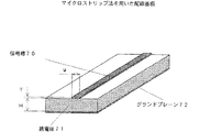
図7において、信号線70と誘電体71とグランドプレーン72とからなるマイクロストリップ線路の特性インピーダンスは、信号線70の幅Wおよび厚さTと、誘電体71の厚さHおよび誘電率とによって規定される。
必要に応じた特性インピーダンスとなるように主に信号線70の幅Wによって調整される。
【0005】
図8は従来のマイクロストリップ線路のパターンを示したものである。
信号線80と対向するグランドプレーン81は、信号線80の全領域に亙って一様の導体面となっている。
【0006】
【発明が解決しようとする課題】
しかしながら、従来のコプラーナ法を用いたプリント配線基板には、電子機器の小型化に伴いプリント配線基板への部品実装密度が高まりプリント配線基板も小型で薄くなっているため、スリット幅がとれず適切なインピーダンスの確保が難しいという課題がある。
【0007】
また、従来のマイクロストリップ法を用いたプリント配線基板には、プリント配線基板が薄くなると等価的にキャパシタンスが大きくなってマイクロストリップ線路の特性インピーダンスを下げてしまうので、信号線の幅を小さくしてキャパシタンスを減らしインダクタンスを大きくして所定の特性インピーダンスを確保しているが、信号線の直流抵抗の増加により伝送特性が悪くなるという課題がある。
【0008】
さらに、従来のマイクロストリップ法を用いたプリント配線基板には、フィルム基板の様に極端に薄いものに対し、信号線の幅を小さくしても物理的に限界があり、マイクロストリップ線路のインピーダンス確保が難しいという課題がある。
【0009】
また、従来のマイクロストリップ法を用いたプリント配線基板には、グランドプレーンをメッシュ構造や、編み目状にしてキャパシタンスを下げる方法もあるが、信号線に対してメッシュ構造や、編み目が大きいので特性インピーダンスが不均一となり、マイクロストリップ線路の伝送特性が悪くなるという課題がある。
【0010】
本発明は、上記した従来技術の課題を解決するためになされたものであって、その目的は、誘電体を挟んで信号線と対向するグランドプレーンの領域にスリットを設けることにより、小型で薄いプリント配線基板に対し、伝送線路の抵抗およびインダクタンスの変化を少なく抑えて特性インピーダンスの制御ができるスリット法を用いた高速信号用プリント配線基板を提供することにある。
【0011】
【課題を解決するための手段】
上記課題を解決するために本発明に係るスリット法を用いた高速信号用プリント配線基板は、誘電体を挟んで信号線と対向するグランドプレーンの領域に信号線に沿ってスリットを設けたので、小型で薄いプリント配線基板に対し、伝送路の抵抗およびインダクタンスを変えることなく特性インピーダンスを制御することができる。
【0012】
また、本発明に係るスリット法を用いた高速信号用プリント配線基板は、第1の誘電体と、第1の誘電体を挟んで一方の面に設けられる信号線と他方の面に設けられるグランドプレーンと、信号線が設けられた第1の誘電体の上層に配される第2の誘電体と、第2の誘電体の他方の面に設けられるグランドプレーンとを備え、信号線と対向する第1および第2の誘電体に設けられるグランドプレーンの領域にスリットを設けたので、小型で薄いプリント配線基板に対し、伝送線路の抵抗およびインダクタンスの変化を少なく抑えて特性インピーダンスの制御ができる。
【0013】
【発明の実施の形態】
本発明の実施の形態を添付図面に基づいて以下に説明する。
図1は本発明に係る2層配線におけるスリット法を用いた高速信号用プリント配線基板1の一実施形態の要部構成図である。
図1において、2層配線におけるスリット法を用いた高速信号用プリント配線基板1は、信号線10、平板状の誘電体11、グランドプレーン12、スリット13とからなる伝送線路を有する。
【0014】
誘電体11を挟んで一方の面に設けた信号線10と、他方の面に設けたグランドプレーン12と、信号線10と対向するグランドプレーン12の領域に設けたスリット13とから構成される伝送線路の特性インピーダンスZ0は、信号線10の幅Wおよび厚さTと、誘電体11の厚さHおよび誘電率と、スリット13の幅W1とよって規定される。
【0015】
一般に、プリント配線基板が薄くなると誘電体11の厚さHの値が小さくなり、等価的にキャパシタンスCが大きくなって特性インピーダンスが下がり、所定の特性インピーダンスZ0の確保が難しくなるが、本発明に係るスリット法を用いた高速信号用プリント配線基板1においてはスリット13の幅W1を調整してキャパシタンスCの値を制御し、所定の特性インピーダンスZ0を確保することができる。
【0016】
この様に、本発明に係るスリット法を用いた高速信号用プリント配線基板1は信号線10と対向するグランドプレーン12領域に信号線10に沿って設けたスリット13の幅W1を調整することにより、フィルム基板の様に極端に薄いものであっても信号線10の幅Wを変化させることなく(信号線10の抵抗RとインダクタンスLの変化は少ない)、伝送線路の所定の特性インピーダンスZ0を確保することができる。
【0017】
図2は本発明に係る多層配線(図例は3層)におけるスリット法を用いた高速信号用プリント配線基板2の一実施形態の要部構成図である。
図2において、3層配線におけるスリット法を用いた高速信号用プリント配線基板2は、信号線20、第1の誘電体21、第1のグランドプレーン22、第1のスリット23、第2の誘電体24、第2のグランドプレーン25、第2のスリット26とからなる伝送線路を有する。
【0018】
信号線20は第1の誘電体21を挟んで一方の面に設けられ、第1のグランドプレーン22は第1の誘電体21の他方の面に設けられ、第1のスリット23は信号線20と対向する第1のグランドプレーン22の領域に信号線20に沿って設けられる。
第2の誘電体24は信号線20を設けた第1の誘電体21の上層に配され、第2のグランドプレーン25は信号線20と接する第2の誘電体24の他方の面に設けられ、第2のスリット26は信号線20と対向する第2のグランドプレーン25の領域に信号線20に沿って設けられる。
【0019】
伝送線路の特性インピーダンスZ0は、信号線20の幅Wおよび厚さTと、第1の誘電体21の厚さH1および其の誘電率と、第1のスリット23の幅W1と、第2の誘電体24の厚さH2および其の誘電率と、第2のスリット26の幅W2とによって規定される。
【0020】
一般に、プリント配線基板が薄くなると誘電体の厚さ(H1、H2)の値が小さくなり、等価的にキャパシタンスCが大きくなって特性インピーダンスが下がり、所定の特性インピーダンスZ0の確保が難しくなるが、本発明に係るスリット法を用いた高速信号用プリント配線基板2においては第1のスリット23の幅W1と第2のスリット26の幅W2とを調整してキャパシタンスCの値を制御し、所定の特性インピーダンスZ0を確保することができる。
【0021】
この様に、本発明に係るスリット法を用いた高速信号用プリント配線基板2は信号線10と対向する第1および第2のグランドプレーン領域に信号線10に沿って設けたスリット(13、26)の幅(W1、W2)を調整することにより、フィルム基板の様に極端に薄いものであっても信号線10の幅Wを変化させることなく(信号線10の抵抗RとインダクタンスLの変化は少ない)、伝送線路の所定の特性インピーダンスZ0を確保することができる。
【0022】
図3−1はマイクロストリップ線路とスリット法を用いた伝送線路の比較説明図である。
図3−1の図1Aと図1Bは従来例として示したマイクロストリップ法を用いた配線基板の模式的断面図であり、図1Cは本発明に係るスリット法を用いた高速信号用プリント配線基板の模式的断面図である。
【0023】
図3−1の図1Aは、誘電体31の上面の信号線30と、誘電体31の下面にあるグランドプレーン50とからなるマイクロストリップ線路を示したものである。
図3−1の図1Bは、1Aの誘電体31に比較して誘電体40の様に厚さが薄くなりキャパシタンスが大きくなった為に、信号線30bに示す様に幅を小さくしてグランドプレーンとの対向面積を小さくすることによってキャパシタンスを小さくし、マイクロストリップ線路の所定の特性インピーダンスを得る。
信号線30bの様に幅を小さくするとキャパシタンスは小さくなるが、信号線30bの抵抗が増大して伝送損失が増し、伝送品質を悪化させる。
【0024】
図3−1の図1Cは本発明に係るスリット法を用いた伝送線路を示したもので、誘電体40の上面の信号線30と対向する誘電体40の下面のグランドプレーン52の領域にスリット53を設けたものである。
この様に誘電体が薄くなってもスリット53を設けることによってキャパシタンスを小さくすることができ、信号線の幅を変えることなく伝送線路の所定の特性インピーダンスを制御することができる。
【0025】
図3−2は2層配線におけるスリット法を用いた伝送線路の説明図である。
この図は、図1に示した2層配線におけるスリット法を用いた高速信号用プリント配線基板1の模式的断面図であり、この図1を用いて誘電体基板の厚さとスリット幅の関係を説明する。
【0026】
図3−2の図(1B〜4B)は図(1A〜4A)に示す誘電体基板の厚さに比較して薄くなった場合の信号線とスリットの関係を示す。
図1Aは誘電体31の上面の信号線30と、誘電体31の下面にあるグランドプレーン32の信号線30と対向する領域に設けられたスリット33との関係を示す。
スリット33の幅Wa1は信号線30の幅より狭く、スリット法を用いた伝送線路の特性インピーダンスをZ0とする。
【0027】
図1Bは薄くなった誘電体40の上面にある信号線30と、誘電体40の下面にあるグランドプレーン41の信号線30と対向する領域に設けられたスリット42との関係を示す。
図1Bにおいて、誘電体40が薄くなり低くなった伝送線路の特性インピーダンスをZ0にするためにスリット42の幅Wb1は、スリット33の幅Wa1よりも広く、信号線30の幅と略等しく調整されていることを示している。
【0028】
図2Aはスリット35の幅Wa2が信号線30の幅と略等しい場合を示しており、図2Bは誘電体40が薄くなり低くなった伝送線路の特性インピーダンスをZ0にするためにスリット43の幅Wb2をスリット35の幅Wa2より広くし、信号線30の幅より広く調整されていることを示している。
【0029】
図3Aはスリット37の幅Wa3が信号線30の幅より広い場合を示しており、図3Bは誘電体40が薄くなり低くなった伝送線路の特性インピーダンスをZ0にするためにスリット45の幅Wb3をスリット37の幅Wa3より広く、信号線30の幅より更に広く調整されていることを示している。
【0030】
図4Aと図4Bは誘電体31に複数のスリット法を用いた伝送線路を形成した場合を示したもので、図(1A〜3A)と図(1B〜3B)で述べたことと同様に其々の伝送線路の特性インピーダンスが調整される。
【0031】
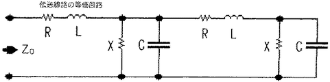
図4は伝送線路の等価回路を示したものである。
伝送線路の等価回路は、抵抗R、インダクタンスL、キャパシタンスC、コンダクタンスXとから構成される。
スリット法を用いた伝送線路の特性インピーダンスZ0は、この等価回路より下記に示す数式で表せる。
【0032】
【数1】
Z0=√(R+jwL/X+jwC)
【0033】
数1より、誘電体が薄くなってキャパシタンスCの値が大きくなると伝送線路の特性インピーダンスZ0は小さくなり、本発明に係るスリットの幅を調整してキャパシタンスCの値を制御することにより、信号線の幅を変化させることなく(抵抗RとインダクタンスLの変化は少ない)、スリット法を用いた伝送線路の特性インピーダンスZ0を調整することができる。
【0034】
図5は、本発明に係るスリット法を用いた伝送線路の信号線とグランドプレーンとスリットとの関係を表すパターンを示したものである。
スリット法を用いた伝送線路を図5に示す信号線55、グランドプレーン57、スリット56の様に構成することによって特性インピーダンスZaとZbとZcを所定の値に調節して等しくすることができる。
【0035】
なお、上記実施の形態は本発明の一例であり、本発明は上記実施の形態に限定されるものではない。
【0036】
【発明の効果】
本発明は上記構成により次の効果を発揮する。
本発明に係るスリット法を用いた高速信号用プリント配線基板1は、信号線10と対向するグランドプレーン12領域に信号線10に沿って設けたスリット13の幅W1を調整することにより、フィルム基板の様に極端に薄いものであっても信号線10の幅Wを変化させることなく(信号線10の抵抗RとインダクタンスLの変化は少ない)、伝送線路の所定の特性インピーダンスZ0を確保し、品質の良い信号伝送ができるので、製品品質の向上および経済性の向上が図れる。
【0037】
また、本発明に係るスリット法を用いた高速信号用プリント配線基板2は信号線20と対向する第1および第2のグランドプレーン領域に信号線10に沿って設けたスリット(23、26)の幅(W1、W2)を調整することにより、フィルム基板の様に極端に薄いものであっても信号線20の幅Wを変化させることなく(抵抗RとインダクタンスLの変化は少ない)、伝送線路の所定の特性インピーダンスZ0を制御することができ、柔軟な基板設計を可能とし、且つ品質の良い信号伝送ができるので、製品品質の向上および経済性の向上が図れる。
【0038】
よって、本発明は、品質が良く、経済性の高いスリット法を用いた高速信号用プリント配線基板を提供することができる。
【図面の簡単な説明】
【図1】本発明に係る2層配線におけるスリット法を用いた高速信号用プリント配線基板1の一実施形態の要部構成図である。
【図2】本発明に係る3層配線におけるスリット法を用いた高速信号用プリント配線基板2の一実施形態の要部構成図である。
【図3−1】マイクロストリップ線路とスリット法を用いた伝送線路の比較説明図である。
【図3−2】本発明に係る2層配線のおけるスリット法を用いた伝送線路の説明図である。
【図4】伝送線路の特性インピーダンスZ0の等価回路である。
【図5】本発明に係るスリット法を用いた伝送線路の信号線とグランドプレーンとスリットとの関係を表すパターンである。
【図6】コプラーナ法を用いたプリント配線基板の要部構成図である。
【図7】マイクロストリップ法を用いたプリント配線基板の要部構成図である。
【図8】マイクロストリップ線路のパターンの模式図である。
【符号の説明】
10、20、30、38、55、60、70,80…信号線
11、31、40、61、71…誘電体
12、32、34、36、39、41、42、
44、48、50、51、52、55、57、
62,72、81 …グランドプレーン
13、33,35,37,43,45,49、53、56、63…スリット
21…第1の誘電体
22…第1のグランドプレーン
23…第1のスリット
24…第2の誘電体
25…第2のグランドプレーン
26…第2のスリット
H…誘電体の厚み
H1…第1の誘電体の厚み
H2…第2の誘電体の厚み
C…キャパシタンス
L…インダクタンス
R…抵抗
T…信号線の厚み
W、Wa1,Wa2,Wa3,Wb1,Wb2,Wb3…信号線の幅
W1…第1の信号線の幅
W2…第2の信号線の幅
Z0、Za、Zb、Zc…特性インピーダンス。[0001]
TECHNICAL FIELD OF THE INVENTION
The present invention relates to a high-speed signal printed wiring board using a slit method suitable for high-speed signal transmission, and in particular, to a high-speed signal using a slit method capable of controlling characteristic impedance while suppressing a change in resistance and inductance of a transmission line to a small value. The present invention relates to a printed wiring board.
[0002]
[Prior art]
As a wiring pattern method for matching the impedance of a transmission line of a printed wiring board for high-speed signals, there are a coplanar method, a microstrip method, a strip method, and the like.
As a conventional example related to the present invention, FIG. 6 is a main part configuration diagram of a printed wiring board using a coplanar method, FIG. 7 is a main part configuration diagram of a printed wiring board using a microstrip method, and FIG. FIG.
[0003]
6, the characteristic impedance of the coplanar line including the signal line 60, the dielectric 61, and the ground plane 62 includes the width W and the thickness T of the signal line 60, the thickness H and the dielectric constant of the dielectric 61, and the slit. 63 is defined by the width S.
The width is adjusted mainly by the width W of the signal line 60 and the width S of the slit 63 so that the characteristic impedance becomes necessary.
[0004]
7, the characteristic impedance of the microstrip line including the signal line 70, the dielectric 71, and the ground plane 72 depends on the width W and the thickness T of the signal line 70 and the thickness H and the dielectric constant of the dielectric 71. Stipulated.
It is adjusted mainly by the width W of the signal line 70 so that the characteristic impedance becomes necessary.
[0005]
FIG. 8 shows a pattern of a conventional microstrip line.
The ground plane 81 facing the signal line 80 has a uniform conductor surface over the entire area of the signal line 80.
[0006]
[Problems to be solved by the invention]
However, conventional printed wiring boards using the coplanar method are not suitable for slit width because the density of components mounted on the printed wiring board has increased due to the miniaturization of electronic devices, and the printed wiring board has also become smaller and thinner. There is a problem that it is difficult to secure a high impedance.
[0007]
Also, in a printed wiring board using a conventional microstrip method, when the thickness of the printed wiring board becomes thinner, equivalently, the capacitance becomes larger and the characteristic impedance of the microstrip line is lowered. Although a predetermined characteristic impedance is ensured by reducing the capacitance and increasing the inductance, there is a problem that the transmission characteristics deteriorate due to an increase in the DC resistance of the signal line.
[0008]
Furthermore, printed wiring boards using the conventional microstrip method are physically limited even if the width of the signal lines is reduced, even though they are extremely thin, such as a film substrate, and the impedance of the microstrip line is secured. There is a problem that is difficult.
[0009]
In a conventional printed wiring board using the microstrip method, there is also a method of reducing the capacitance by forming a ground plane into a mesh structure or a stitch shape. However, since the mesh structure and the stitch are large with respect to the signal line, the characteristic impedance is reduced. And the transmission characteristics of the microstrip line are deteriorated.
[0010]
The present invention has been made in order to solve the above-described problems of the related art, and an object thereof is to provide a slit in a region of a ground plane opposed to a signal line with a dielectric interposed therebetween, so that the device is small and thin. An object of the present invention is to provide a high-speed signal printed circuit board using a slit method that can control characteristic impedance while suppressing a change in resistance and inductance of a transmission line to a printed circuit board.
[0011]
[Means for Solving the Problems]
In order to solve the above problems, the high-speed signal printed wiring board using the slit method according to the present invention, since the slit is provided along the signal line in the region of the ground plane facing the signal line across the dielectric, The characteristic impedance of a small and thin printed wiring board can be controlled without changing the resistance and inductance of the transmission line.
[0012]
Further, a high-speed signal printed wiring board using the slit method according to the present invention includes a first dielectric, a signal line provided on one surface with the first dielectric interposed therebetween, and a ground provided on the other surface. A plane, a second dielectric disposed on an upper layer of the first dielectric on which the signal line is provided, and a ground plane provided on the other surface of the second dielectric, facing the signal line Since the slit is provided in the area of the ground plane provided in the first and second dielectrics, the characteristic impedance can be controlled with a small change in the resistance and inductance of the transmission line for a small and thin printed wiring board.
[0013]
BEST MODE FOR CARRYING OUT THE INVENTION
Embodiments of the present invention will be described below with reference to the accompanying drawings.
FIG. 1 is a configuration diagram of a main part of an embodiment of a high-speed signal printed
In FIG. 1, a high-speed signal printed
[0014]
A transmission composed of a signal line 10 provided on one surface with a dielectric 11 interposed therebetween, a ground plane 12 provided on the other surface, and a slit 13 provided in a region of the ground plane 12 facing the signal line 10. The characteristic impedance Z0 of the line is defined by the width W and thickness T of the signal line 10, the thickness H and dielectric constant of the dielectric 11, and the width W1 of the slit 13.
[0015]
In general, as the thickness of the printed wiring board becomes thinner, the value of the thickness H of the dielectric 11 becomes smaller, the capacitance C becomes equivalently larger, the characteristic impedance decreases, and it becomes difficult to secure a predetermined characteristic impedance Z0. In the high-speed signal printed
[0016]
As described above, the printed
[0017]
FIG. 2 is a main part configuration diagram of one embodiment of a high-speed signal printed wiring board 2 using a slit method in a multilayer wiring (three layers in the figure) according to the present invention.
In FIG. 2, a high-speed signal printed wiring board 2 using a slit method in three-layer wiring includes a
[0018]
The
The second dielectric 24 is provided on the first dielectric 21 on which the
[0019]
The characteristic impedance Z0 of the transmission line includes the width W and thickness T of the
[0020]
In general, when the thickness of the printed wiring board is reduced, the value of the thickness (H1, H2) of the dielectric material is reduced, the capacitance C is equivalently increased, the characteristic impedance is reduced, and it is difficult to secure a predetermined characteristic impedance Z0. In the printed wiring board 2 for high-speed signals using the slit method according to the present invention, the value of the capacitance C is controlled by adjusting the width W1 of the first slit 23 and the width W2 of the second slit 26, and The characteristic impedance Z0 can be secured.
[0021]
As described above, the printed wiring board 2 for high-speed signal using the slit method according to the present invention has slits (13, 26) provided along the signal line 10 in the first and second ground plane regions facing the signal line 10. ) Can be adjusted without changing the width W of the signal line 10 (the change in the resistance R and the inductance L of the signal line 10) even if the width is extremely thin like a film substrate. Is small), and a predetermined characteristic impedance Z0 of the transmission line can be secured.
[0022]
FIG. 3-1 is a comparative explanatory diagram of a microstrip line and a transmission line using a slit method.
FIGS. 1A and 1B are schematic cross-sectional views of a wiring board using a microstrip method shown as a conventional example, and FIG. 1C is a printed wiring board for high-speed signals using a slit method according to the present invention. FIG. 3 is a schematic sectional view of FIG.
[0023]
FIG. 1A of FIG. 3A shows a microstrip line including a
FIG. 1B of FIG. 3A shows that the width is reduced as shown by the signal line 30b because the thickness is reduced and the capacitance is increased like the dielectric 40 as compared with the dielectric 31 of 1A. The capacitance is reduced by reducing the area facing the plane, and a predetermined characteristic impedance of the microstrip line is obtained.
When the width is reduced like the signal line 30b, the capacitance is reduced, but the resistance of the signal line 30b is increased, transmission loss is increased, and transmission quality is deteriorated.
[0024]
FIG. 1C of FIG. 3A shows a transmission line using the slit method according to the present invention, and a slit is formed in a region of a ground plane 52 on the lower surface of the dielectric 40 facing the
Thus, even if the dielectric material becomes thin, the provision of the slit 53 makes it possible to reduce the capacitance and control the predetermined characteristic impedance of the transmission line without changing the width of the signal line.
[0025]
FIG. 3-2 is an explanatory diagram of a transmission line using a slit method in two-layer wiring.
This figure is a schematic cross-sectional view of a high-speed signal printed
[0026]
FIGS. 3A to 3C show the relationship between the signal lines and the slits when the thickness is smaller than the thickness of the dielectric substrate shown in FIGS. 1A to 4A.
FIG. 1A shows a relationship between a
The width Wa1 of the slit 33 is smaller than the width of the
[0027]
FIG. 1B shows a relationship between the
In FIG. 1B, the width Wb1 of the slit 42 is larger than the width Wa1 of the slit 33 and is adjusted to be substantially equal to the width of the
[0028]
FIG. 2A shows a case where the width Wa2 of the slit 35 is substantially equal to the width of the
[0029]
3A shows a case where the width Wa3 of the slit 37 is wider than the width of the
[0030]
FIGS. 4A and 4B show a case where a transmission line using a plurality of slit methods is formed in the dielectric material 31. As shown in FIGS. 1A to 3A and FIGS. 1B to 3B, FIG. The characteristic impedance of each transmission line is adjusted.
[0031]
FIG. 4 shows an equivalent circuit of the transmission line.
The equivalent circuit of the transmission line includes a resistance R, an inductance L, a capacitance C, and a conductance X.
The characteristic impedance Z0 of the transmission line using the slit method can be expressed by the following equation from this equivalent circuit.
[0032]
(Equation 1)
Z0 = √ (R + jwL / X + jwC)
[0033]
According to
[0034]
FIG. 5 shows a pattern representing a relationship between a signal line of a transmission line, a ground plane, and a slit using the slit method according to the present invention.
By configuring the transmission line using the slit method like the signal line 55, the ground plane 57, and the slit 56 shown in FIG. 5, the characteristic impedances Za, Zb, and Zc can be adjusted to predetermined values to be equal.
[0035]
The above embodiment is an example of the present invention, and the present invention is not limited to the above embodiment.
[0036]
【The invention's effect】
The present invention has the following effects by the above configuration.
The printed
[0037]
In addition, the high-speed signal printed wiring board 2 using the slit method according to the present invention has slits (23, 26) provided along the signal lines 10 in the first and second ground plane regions facing the signal lines 20. By adjusting the widths (W1, W2), the transmission line can be formed without changing the width W of the signal line 20 (the resistance R and the inductance L are small) even if it is extremely thin like a film substrate. Can be controlled, a flexible board design is possible, and high-quality signal transmission can be performed, so that the product quality and the economic efficiency can be improved.
[0038]
Therefore, the present invention can provide a high-speed signal printed wiring board using a slit method with good quality and high cost.
[Brief description of the drawings]
FIG. 1 is a main part configuration diagram of one embodiment of a high-speed signal printed
FIG. 2 is a main part configuration diagram of one embodiment of a high-speed signal printed wiring board 2 using a slit method in three-layer wiring according to the present invention.
FIG. 3-1 is a comparative explanatory diagram of a microstrip line and a transmission line using a slit method.
FIG. 3-2 is an explanatory diagram of a transmission line using a slit method in a two-layer wiring according to the present invention.
FIG. 4 is an equivalent circuit of a characteristic impedance Z0 of a transmission line.
FIG. 5 is a pattern showing a relationship between a signal line of a transmission line, a ground plane, and a slit using the slit method according to the present invention.
FIG. 6 is a configuration diagram of a main part of a printed wiring board using a coplanar method.
FIG. 7 is a configuration diagram of a main part of a printed wiring board using a microstrip method.
FIG. 8 is a schematic diagram of a pattern of a microstrip line.
[Explanation of symbols]
10, 20, 30, 38, 55, 60, 70, 80 ...
44, 48, 50, 51, 52, 55, 57,
62, 72, 81 ... ground planes 13, 33, 35, 37, 43, 45, 49, 53, 56, 63 ... slits 21 ... first dielectric 22 ... first ground plane 23 ... first slits 24 ... second dielectric 25 ... second ground plane 26 ... second slit H ... dielectric thickness H1 ... first dielectric thickness H2 ... second dielectric thickness C ... capacitance L ... inductance R ... Resistance T ... Thickness W of signal lines, Wa1, Wa2, Wa3, Wb1, Wb2, Wb3 ... Width W1 of signal lines ... Width W2 of first signal lines ... Zc: characteristic impedance.
Claims (4)
前記信号線と対向する前記グランドプレーン領域にスリットを設けたことを特徴とするスリット法を用いた高速信号用プリント配線基板。A high-speed signal printed wiring board using a slit method comprising a plate-shaped dielectric and a signal line provided on one surface and a ground plane provided on the other surface sandwiching the dielectric,
A high-speed signal printed wiring board using a slit method, wherein a slit is provided in the ground plane region facing the signal line.
前記信号線と対向する第1のグランドプレーン領域に第1のスリットを設け、さらに前記信号線と対向する第2のグランドプレーン領域に第2のスリットを設けたことを特徴とするスリット法を用いた高速信号用プリント配線基板。A plate-shaped first dielectric, a signal line provided on one surface and a first ground plane provided on the other surface with the first dielectric interposed therebetween, and a first ground plane provided with the signal line. A second dielectric having a flat plate shape disposed on an upper layer of the first dielectric and a second ground plane provided on the other surface of the second dielectric having one surface in contact with a signal line; In the printed wiring board for high-speed signals using the slit method,
A first slit is provided in a first ground plane region facing the signal line, and a second slit is further provided in a second ground plane region facing the signal line. Printed circuit board for high-speed signals.
Priority Applications (1)
| Application Number | Priority Date | Filing Date | Title |
|---|---|---|---|
| JP2002337298A JP2004140308A (en) | 2002-10-16 | 2002-10-16 | Printed wiring board for high-speed signal using slit method |
Applications Claiming Priority (1)
| Application Number | Priority Date | Filing Date | Title |
|---|---|---|---|
| JP2002337298A JP2004140308A (en) | 2002-10-16 | 2002-10-16 | Printed wiring board for high-speed signal using slit method |
Publications (1)
| Publication Number | Publication Date |
|---|---|
| JP2004140308A true JP2004140308A (en) | 2004-05-13 |
Family
ID=32462645
Family Applications (1)
| Application Number | Title | Priority Date | Filing Date |
|---|---|---|---|
| JP2002337298A Pending JP2004140308A (en) | 2002-10-16 | 2002-10-16 | Printed wiring board for high-speed signal using slit method |
Country Status (1)
| Country | Link |
|---|---|
| JP (1) | JP2004140308A (en) |
Cited By (15)
| Publication number | Priority date | Publication date | Assignee | Title |
|---|---|---|---|---|
| JP2008112862A (en) * | 2006-10-30 | 2008-05-15 | Nec Saitama Ltd | Double-side printed wiring circuit board, electronic device, and method of manufacturing the double-side printed wiring circuit board |
| WO2008149572A1 (en) * | 2007-06-06 | 2008-12-11 | Nippon Mektron, Ltd. | Printed wiring board |
| JP2009038341A (en) * | 2007-07-09 | 2009-02-19 | Canon Inc | Printed circuit board |
| WO2009102108A1 (en) * | 2008-02-15 | 2009-08-20 | Gigalane Co.Ltd | Printed circuit board |
| JP2009266903A (en) * | 2008-04-22 | 2009-11-12 | Opnext Japan Inc | Optical communication module and flexible printed board |
| JP2010506387A (en) * | 2006-10-06 | 2010-02-25 | エプコス アクチエンゲゼルシャフト | Substrate with high frequency compatibility line |
| KR100958268B1 (en) * | 2008-02-15 | 2010-05-19 | (주)기가레인 | printed circuit board capable of widening the width of signal transmission line without impedance miss matching |
| JP2011114263A (en) * | 2009-11-30 | 2011-06-09 | Kyocer Slc Technologies Corp | Wiring board |
| JP2013520797A (en) * | 2010-02-19 | 2013-06-06 | アルテラ コーポレイション | Shield structure for transmission lines |
| JP2014179535A (en) * | 2013-03-15 | 2014-09-25 | Fujitsu Component Ltd | Circuit board and method of manufacturing the same |
| JP2014194948A (en) * | 2012-07-30 | 2014-10-09 | Murata Mfg Co Ltd | Flat cable |
| US8993892B2 (en) | 2011-01-24 | 2015-03-31 | Brother Kogyo Kabushiki Kaisha | Wiring board and method of manufacturing the wiring board |
| US9185104B2 (en) | 2007-08-16 | 2015-11-10 | Samsung Electronics Co., Ltd. | Method and apparatus for communication, and method and apparatus for controlling communication |
| CN105430873A (en) * | 2009-12-23 | 2016-03-23 | 上海贝尔股份有限公司 | High-speed connector package and packaging method |
| JPWO2017090181A1 (en) * | 2015-11-27 | 2018-09-06 | 富士通株式会社 | Circuit board and electronic device |
-
2002
- 2002-10-16 JP JP2002337298A patent/JP2004140308A/en active Pending
Cited By (23)
| Publication number | Priority date | Publication date | Assignee | Title |
|---|---|---|---|---|
| JP2010506387A (en) * | 2006-10-06 | 2010-02-25 | エプコス アクチエンゲゼルシャフト | Substrate with high frequency compatibility line |
| JP2008112862A (en) * | 2006-10-30 | 2008-05-15 | Nec Saitama Ltd | Double-side printed wiring circuit board, electronic device, and method of manufacturing the double-side printed wiring circuit board |
| WO2008149572A1 (en) * | 2007-06-06 | 2008-12-11 | Nippon Mektron, Ltd. | Printed wiring board |
| JP2008305884A (en) * | 2007-06-06 | 2008-12-18 | Nippon Mektron Ltd | Printed circuit board |
| EP2031944A1 (en) * | 2007-06-06 | 2009-03-04 | Nippon Mektron, Limited | Printed wiring board |
| US8040198B2 (en) | 2007-06-06 | 2011-10-18 | Nippon Mektron, Ltd. | Printed wiring board having wire grounding conductors with distances that are 1/n the width of the signal lines |
| EP2031944A4 (en) * | 2007-06-06 | 2009-12-09 | Nippon Mektron Kk | Printed wiring board |
| TWI403226B (en) * | 2007-06-06 | 2013-07-21 | Nippon Mektron Kk | Printed wiring board |
| JP2009038341A (en) * | 2007-07-09 | 2009-02-19 | Canon Inc | Printed circuit board |
| US9185104B2 (en) | 2007-08-16 | 2015-11-10 | Samsung Electronics Co., Ltd. | Method and apparatus for communication, and method and apparatus for controlling communication |
| KR100958268B1 (en) * | 2008-02-15 | 2010-05-19 | (주)기가레인 | printed circuit board capable of widening the width of signal transmission line without impedance miss matching |
| US8013254B2 (en) | 2008-02-15 | 2011-09-06 | Gigalane Co. Ltd. | Printed circuit board |
| WO2009102108A1 (en) * | 2008-02-15 | 2009-08-20 | Gigalane Co.Ltd | Printed circuit board |
| JP2009266903A (en) * | 2008-04-22 | 2009-11-12 | Opnext Japan Inc | Optical communication module and flexible printed board |
| JP2011114263A (en) * | 2009-11-30 | 2011-06-09 | Kyocer Slc Technologies Corp | Wiring board |
| CN105430873A (en) * | 2009-12-23 | 2016-03-23 | 上海贝尔股份有限公司 | High-speed connector package and packaging method |
| JP2013520797A (en) * | 2010-02-19 | 2013-06-06 | アルテラ コーポレイション | Shield structure for transmission lines |
| US8993892B2 (en) | 2011-01-24 | 2015-03-31 | Brother Kogyo Kabushiki Kaisha | Wiring board and method of manufacturing the wiring board |
| JP2014194948A (en) * | 2012-07-30 | 2014-10-09 | Murata Mfg Co Ltd | Flat cable |
| US9130251B2 (en) | 2012-07-30 | 2015-09-08 | Murata Manufacturing Co., Ltd. | Flat cable |
| JP2014179535A (en) * | 2013-03-15 | 2014-09-25 | Fujitsu Component Ltd | Circuit board and method of manufacturing the same |
| JPWO2017090181A1 (en) * | 2015-11-27 | 2018-09-06 | 富士通株式会社 | Circuit board and electronic device |
| US10306757B2 (en) | 2015-11-27 | 2019-05-28 | Fujitsu Limited | Circuit board and electronic device |
Similar Documents
| Publication | Publication Date | Title |
|---|---|---|
| JP2004140308A (en) | Printed wiring board for high-speed signal using slit method | |
| JP3732927B2 (en) | Multilayer wiring board | |
| US20050146390A1 (en) | Multi-layer substrate having impedance-matching hole | |
| JPH06302964A (en) | Circuit board for high-speed signal transmission | |
| US8558120B2 (en) | Multilayer board for suppressing unwanted electromagnetic waves and noise | |
| US9301386B2 (en) | Printed circuit board and method of manufacturing the same | |
| JP2001144451A (en) | Laminated wiring board | |
| JP2001144452A (en) | Multilayered printed board | |
| JP4161577B2 (en) | Electrical wiring board | |
| JPH06260773A (en) | Pad structure of high speed signal transmission circuit board | |
| JP2007165755A (en) | Wiring board and method for manufacturing the same | |
| JP2500783B2 (en) | Printed board | |
| JPS61290794A (en) | Wiring board | |
| JP3297447B2 (en) | High frequency multilayer circuit board adjustment method | |
| JP2002057467A (en) | Multilayered printed circuit board | |
| JP2002076644A (en) | Multilayer printed wiring board | |
| JP6222747B2 (en) | Circuit structure | |
| JP3077487B2 (en) | High frequency circuit | |
| JP2006080162A (en) | Printed wiring board | |
| JPH04261022A (en) | Semiconductor integrated circuit | |
| JP4032609B2 (en) | Adjustment method of chip antenna | |
| JP2006080239A (en) | Laminated high-frequency circuit board | |
| JP3249766B2 (en) | Flexible printed circuit board | |
| JP2005236064A (en) | Signal transmission pair wiring and its manufacturing method | |
| JPS60253303A (en) | Microstrip line |
Legal Events
| Date | Code | Title | Description |
|---|---|---|---|
| A621 | Written request for application examination |
Free format text: JAPANESE INTERMEDIATE CODE: A621 Effective date: 20050114 |
|
| A131 | Notification of reasons for refusal |
Free format text: JAPANESE INTERMEDIATE CODE: A131 Effective date: 20070306 |
|
| A02 | Decision of refusal |
Free format text: JAPANESE INTERMEDIATE CODE: A02 Effective date: 20070703 |