JP2004140160A - Wiring board, method for manufacturing the same and semiconductor device - Google Patents
Wiring board, method for manufacturing the same and semiconductor device Download PDFInfo
- Publication number
- JP2004140160A JP2004140160A JP2002303015A JP2002303015A JP2004140160A JP 2004140160 A JP2004140160 A JP 2004140160A JP 2002303015 A JP2002303015 A JP 2002303015A JP 2002303015 A JP2002303015 A JP 2002303015A JP 2004140160 A JP2004140160 A JP 2004140160A
- Authority
- JP
- Japan
- Prior art keywords
- wiring
- wiring board
- insulating adhesive
- insulator
- conductor plate
- Prior art date
- Legal status (The legal status is an assumption and is not a legal conclusion. Google has not performed a legal analysis and makes no representation as to the accuracy of the status listed.)
- Granted
Links
Images


Classifications
-
- H—ELECTRICITY
- H01—ELECTRIC ELEMENTS
- H01L—SEMICONDUCTOR DEVICES NOT COVERED BY CLASS H10
- H01L2224/00—Indexing scheme for arrangements for connecting or disconnecting semiconductor or solid-state bodies and methods related thereto as covered by H01L24/00
- H01L2224/01—Means for bonding being attached to, or being formed on, the surface to be connected, e.g. chip-to-package, die-attach, "first-level" interconnects; Manufacturing methods related thereto
- H01L2224/42—Wire connectors; Manufacturing methods related thereto
- H01L2224/47—Structure, shape, material or disposition of the wire connectors after the connecting process
- H01L2224/48—Structure, shape, material or disposition of the wire connectors after the connecting process of an individual wire connector
- H01L2224/4805—Shape
- H01L2224/4809—Loop shape
- H01L2224/48091—Arched
-
- H—ELECTRICITY
- H01—ELECTRIC ELEMENTS
- H01L—SEMICONDUCTOR DEVICES NOT COVERED BY CLASS H10
- H01L2224/00—Indexing scheme for arrangements for connecting or disconnecting semiconductor or solid-state bodies and methods related thereto as covered by H01L24/00
- H01L2224/01—Means for bonding being attached to, or being formed on, the surface to be connected, e.g. chip-to-package, die-attach, "first-level" interconnects; Manufacturing methods related thereto
- H01L2224/42—Wire connectors; Manufacturing methods related thereto
- H01L2224/47—Structure, shape, material or disposition of the wire connectors after the connecting process
- H01L2224/48—Structure, shape, material or disposition of the wire connectors after the connecting process of an individual wire connector
- H01L2224/481—Disposition
- H01L2224/48151—Connecting between a semiconductor or solid-state body and an item not being a semiconductor or solid-state body, e.g. chip-to-substrate, chip-to-passive
- H01L2224/48221—Connecting between a semiconductor or solid-state body and an item not being a semiconductor or solid-state body, e.g. chip-to-substrate, chip-to-passive the body and the item being stacked
- H01L2224/48225—Connecting between a semiconductor or solid-state body and an item not being a semiconductor or solid-state body, e.g. chip-to-substrate, chip-to-passive the body and the item being stacked the item being non-metallic, e.g. insulating substrate with or without metallisation
- H01L2224/48227—Connecting between a semiconductor or solid-state body and an item not being a semiconductor or solid-state body, e.g. chip-to-substrate, chip-to-passive the body and the item being stacked the item being non-metallic, e.g. insulating substrate with or without metallisation connecting the wire to a bond pad of the item
-
- H—ELECTRICITY
- H01—ELECTRIC ELEMENTS
- H01L—SEMICONDUCTOR DEVICES NOT COVERED BY CLASS H10
- H01L2224/00—Indexing scheme for arrangements for connecting or disconnecting semiconductor or solid-state bodies and methods related thereto as covered by H01L24/00
- H01L2224/01—Means for bonding being attached to, or being formed on, the surface to be connected, e.g. chip-to-package, die-attach, "first-level" interconnects; Manufacturing methods related thereto
- H01L2224/42—Wire connectors; Manufacturing methods related thereto
- H01L2224/47—Structure, shape, material or disposition of the wire connectors after the connecting process
- H01L2224/48—Structure, shape, material or disposition of the wire connectors after the connecting process of an individual wire connector
- H01L2224/484—Connecting portions
- H01L2224/4847—Connecting portions the connecting portion on the bonding area of the semiconductor or solid-state body being a wedge bond
- H01L2224/48471—Connecting portions the connecting portion on the bonding area of the semiconductor or solid-state body being a wedge bond the other connecting portion not on the bonding area being a ball bond, i.e. wedge-to-ball, reverse stitch
-
- H—ELECTRICITY
- H01—ELECTRIC ELEMENTS
- H01L—SEMICONDUCTOR DEVICES NOT COVERED BY CLASS H10
- H01L2224/00—Indexing scheme for arrangements for connecting or disconnecting semiconductor or solid-state bodies and methods related thereto as covered by H01L24/00
- H01L2224/73—Means for bonding being of different types provided for in two or more of groups H01L2224/10, H01L2224/18, H01L2224/26, H01L2224/34, H01L2224/42, H01L2224/50, H01L2224/63, H01L2224/71
- H01L2224/732—Location after the connecting process
- H01L2224/73251—Location after the connecting process on different surfaces
- H01L2224/73265—Layer and wire connectors
-
- H—ELECTRICITY
- H01—ELECTRIC ELEMENTS
- H01L—SEMICONDUCTOR DEVICES NOT COVERED BY CLASS H10
- H01L2924/00—Indexing scheme for arrangements or methods for connecting or disconnecting semiconductor or solid-state bodies as covered by H01L24/00
- H01L2924/0001—Technical content checked by a classifier
- H01L2924/00014—Technical content checked by a classifier the subject-matter covered by the group, the symbol of which is combined with the symbol of this group, being disclosed without further technical details
Abstract
Description
【0001】
【発明の属する技術分野】
本発明は、配線板の製造方法及び配線板、ならびに半導体装置に関し、特に、放熱用の導体板(以下、放熱板と称する)を有する配線板の製造方法に適用して有効な技術に関するものである。
【0002】
【従来の技術】
従来、配線板上に半導体チップが実装された半導体装置には、前記半導体チップで発生する熱を外部に放出するための放熱板が設けられた半導体装置がある。前記放熱板が設けられた半導体装置には、例えば、TBGA(Tape Ball Grid Array)と呼ばれる半導体装置がある。
【0003】
前記TBGAと呼ばれる半導体装置には、例えば、絶縁基板の表面に配線(導体パターン)が設けられた配線板と、前記配線板に接着された放熱板と、前記配線板及び前記放熱板に設けられた凹部に収容された半導体チップとからなる半導体装置がある(例えば、非特許文献1参照。)。
【0004】
前記非特許文献1に示されているTBGA型の半導体装置では、例えば、図16に示すように、前記絶縁基板14の第1主面及びその裏面(以下、第2主面と称する)に配線2が設けられている。このとき、前記絶縁基板14の第2主面側の配線2、言い換えると、放熱板3が接着された面側の配線2は、例えば、グラウンド電位にする配線が全面的に設けられている。以下、前記絶縁基板14の第2主面側の配線をグラウンド面2Gと称する。このとき、前記絶縁基板14の第1主面の配線2と前記グラウンド面2Gとは、例えば、前記絶縁基板14に形成されたブラインドビアホールの内部に設けられた導体(ビア)2A、あるいはめっきスルーホールにより電気的に接続されている。
【0005】
前記非特許文献1に示されているTBGA型の半導体装置を製造するときには、大きく分けて、前記半導体装置に用いる配線板を形成する配線板形成工程と、前記配線板形成工程で形成された配線板に半導体チップを実装する半導体チップ実装工程がある。
【0006】
前記配線板形成工程は、まず、例えば、ポリイミドテープなどのテープ状の絶縁基板14の第1主面及び第2主面に導体膜を形成した後、あらかじめ定められた位置に、前記絶縁基板14の第1主面及び前記第2主面に設けられた各導体膜を電気的に接続するビア2Aあるいはめっきスルーホールを形成する。次に、前記各導体膜の不要な部分を除去して前記配線2や前記グラウンド面2Gを形成し、前記絶縁基板14の半導体チップを収容する領域に開口部を形成する。次に、前記配線2及び前記グラウンド面2Gの表面に、例えば、はんだ保護膜(ソルダレジスト)などの保護膜や、はんだめっきなどの接合材を形成する。その後、前記配線板の第2主面、言い換えると前記グラウンド面2Gが形成された面に、絶縁性接着剤15を用いて放熱板3を接着する。このとき、前記放熱板3には、前記配線板の開口部と対応する凹部(座ぐり)3Aを形成しておく。
【0007】
また、前記半導体チップ実装工程では、まず、前記配線板の開口部(デバイスホール)5の内部に半導体チップ9を配置し、前記放熱板3の凹部3Aの底面に前記半導体チップ9を接着する。次に、前記配線2のインナーリード部2Bと前記半導体チップ9の外部電極901とをボンディングワイヤ10で電気的に接続し、前記半導体チップ9及び前記ボンディングワイヤ10による接続部を絶縁樹脂(モールド樹脂)11で封止する。その後、前記配線板の定められた位置に、ボール状の外部接続端子12を形成する。
【0008】
また、前記放熱板3を設けた半導体装置には、前記非特許文献1に示された形態の半導体装置の他に、例えば、銅又はアルミニウムを主成分とする金属板からなるメタルベース上に、有機系絶縁体からなる絶縁層を介して薄膜パターンが設けられた配線板を用いたMBGA(Metal Ball Grid Array)と呼ばれる半導体装置がある(例えば、特許文献1参照。)。
【0009】
【非特許文献1】
大高達也,杉本洋,大森智夫,鈴木幸雄、「画像処理および通信システムLSI搭載用TBGA(Tape Ball Grid Array)」、日立電線、日立電線株式会社、2000年1月、No19、p.79−84
【特許文献1】
特開平08−306820号公報(第6項、第4図)
【0010】
【発明が解決しようとする課題】
しかしながら、前記従来の技術のうち、前記非特許文献1に記載された形態の半導体装置に用いる配線板の製造工程には、前記絶縁基板の第1主面及び前記第2主面に導体膜を張り合わせる工程と、前記放熱板を張り合わせる工程がある。このとき、前記導体膜を張り合わせる工程や前記放熱板を張り合わせる工程では、一般に、フィルム状(シート状)の接着剤を用いるか、あるいは前記絶縁基板又は前記導体膜、前記放熱板などの表面に接着剤を塗布する工程が必要である。そのため、工程数が増えるとともに、材料費が増え、前記配線板の製造コストが上昇するという問題があった。
【0011】
また、前記非特許文献1に記載されたTBGA型の半導体装置では、一般に、前記配線板の厚さが75μmから150μm程度、前記放熱板3の厚さが300μmから800μm程度である。また、前記配線板と前記放熱板3を接着する絶縁性接着剤15の厚さは50μmから100μm程度である。また、前記ボール状の外部接続端子12は、例えば、直径が650μm程度のはんだボールを用いて形成される。そのため、前記半導体装置の厚さT6は1mm以上となり、半導体装置の薄型化が難しいという問題があった。
【0012】
また、前記特許文献1に記載された形態(MBGA型)の半導体装置の場合、前記半導体チップを実装する面と、前記ボール状の外部接続端子を形成する面が異なるとともに、前記半導体チップを実装した面に、中空状のキャップをかぶせている。そのため、半導体装置の薄型化が難しいという問題があった。
【0013】
本発明の目的は、放熱板を有する配線板の製造コストを低減することが可能な技術を提供することにある。
【0014】
本発明の他の目的は、放熱板を有する配線板を用いた半導体装置の薄型化が可能な技術を提供することにある。
【0015】
本発明の前記ならびにその他の目的と新規な特徴は、本明細書の記述及び添付図面によって明らかになるであろう。
【0016】
【課題を解決するための手段】
本願において開示される発明の概要を説明すれば、以下の通りである。
【0017】
(1)絶縁体の表面、もしくは表面及び内部に配線(導体パターン)が形成され、前記絶縁体の一表面に、放熱用の導体板が形成された配線板の製造方法であって、前記導体板の一表面に、絶縁性接着材料を用いて導体膜を接着し、前記導体膜の不要な部分を除去して前記配線を形成した後、前記絶縁性接着材料のあらかじめ定められた領域を開口するとともに、前記導体板の、前記絶縁性接着材料との接着面側の、前記絶縁性接着材料の開口した領域と重なる領域に凹部を形成する配線板の製造方法である。
【0018】
前記(1)の手段によれば、前記放熱用の導体板に前記絶縁性接着材料で接着した導体膜を用いて前記配線を形成することにより、従来の、例えば、前記非特許文献1に記載された配線板の製造方法に比べて、製造工程及び材料費を低減することができる。そのため、前記配線板の製造コストを低減することができる。
【0019】
また、前記(1)の手段において、前記配線を形成する前に、あらかじめ定められた位置で、前記導体膜と前記導体板を電気的に接続してもよい。この場合、前記導体膜の不要な部分を除去して配線を形成したときに、前記配線のうち、例えば、グラウンド電位(接地電位)や電源電位などの、特定の電位の配線と前記放熱用の導体板が接続されるようにすれば、前記放熱用の導体板をグラウンド層(面)として用いることができ、マイクロストリップと呼ばれる形態の伝送路を有する配線板を容易に製造することができる。
【0020】
また、前記(1)の手段を用いた場合、前記配線を形成する前、もしくは前記配線を形成した後、前記導体板の不要な部分を除去して、前記絶縁性接着材料の開口部を覆う放熱用の導体板と、前記導体板と電気的に分離された外部接続端子(ランド)を形成することもできる。このとき、前記外部接続端子は、前記放熱用の導体板と同じ厚さであり、前記配線の厚さに比べて十分に厚い。また、前記外部接続端子は、前記放熱用の導体板と同じ材料であるため、めっきなどで形成する端子(配線)に比べて、表面の平坦性が高い。そのため、前記配線板を用いて半導体装置を製造したときに、前記外部接続端子と他の配線板(実装基板)の配線(端子)との接続性を良くすることができる。
【0021】
また、前記(1)の手段において、前記絶縁性接着材料には、例えば、イミド系樹脂のような高耐熱性接着剤を用いることが好ましい。このとき、前記高耐熱性接着剤は、例えば、前記導体膜の表面、あるいは前記導体板の表面に形成(塗布)しておき、熱プレスにより接着する。
【0022】
また、前記絶縁性接着材料には、フィルム状の絶縁板の両面に絶縁性の接着剤が形成された3層構造の接着フィルムを用いることもできる。前記接着フィルムの場合、中央の前記フィルム状の絶縁板がコア(芯)の役割をするため、接着後の、前記導体膜及び前記絶縁性接着材料、ならびに前記導体板からなる積層体の厚さのばらつきを低減することができる。
【0023】
(2)絶縁体の表面、もしくは表面及び内部に配線(導体パターン)が設けられ、前記絶縁体の一表面に放熱用の導体板が設けられてなり、前記絶縁体は、あらかじめ定められた領域が開口しており、前記放熱用の導体板は、前記絶縁体の開口部を覆うように設けられ、且つ前記絶縁体との接着面側の、前記絶縁体の開口した領域と重なる領域に凹部が設けられた配線板であって、前記配線は、前記放熱性の導体板の一表面上に、絶縁性接着材料で接着されている配線板である。
【0024】
前記(2)の手段によれば、前記配線が、前記放熱用の導体板の一表面上に接着されているので、従来の、絶縁基板の表面に配線を形成した後、接着剤を用いて前記絶縁基板に放熱板を接着した配線板に比べて、薄型化することができる。
【0025】
また、前記(2)の手段において、前記放熱用の導体板を、あらかじめ定められた配線と電気的に接続することにより、例えば、前記放熱用の導体板をグラウンド層(面)とすることができ、マイクロストリップと呼ばれる形態の伝送路を持つ配線板にすることができる。そのため、高周波信号(電流)を伝送したときの信号の劣化や伝送ロス、遅延を少なくすることができる。
【0026】
また、前記(2)の手段において、前記絶縁性接着材料の、前記放熱用の導体板が設けられた面に、前記放熱用の導体板と電気的に分離され、且つ前記配線と電気的に接続された外部接続端子(ランド)が設けてもよい。このとき、前記配線板を用いて製造した半導体装置はLGA(Land Grid Array)と呼ばれる形態にすることができる。
【0027】
また、前記絶縁性接着材料として、フィルム状の絶縁板の両面に絶縁性の接着剤が形成された3層構造の接着フィルムを用いると、中央の前記フィルム状の絶縁板がコア(芯)の役割をするため、前記配線板の厚さのばらつきを低減することができる。
【0028】
(3)絶縁体の表面、もしくは表面及び内部に配線(導体パターン)が設けられ、前記絶縁体の一表面に放熱用の導体板が設けられた配線板と、前記配線板上に設けられた半導体チップと、前記配線板の配線と前記半導体チップの外部電極とを電気的に接続するボンディングワイヤとを備え、前記絶縁体は、あらかじめ定められた領域が開口しており、前記放熱用の導体板は、前記絶縁体の開口部を覆うように設けられ、且つ前記絶縁体との接着面側の、前記絶縁体の開口した領域と重なる領域に凹部が設けられており、前記半導体チップは、前記放熱用の導体板に設けられた前記凹部の底面に接着されている半導体装置であって、前記配線は、前記放熱用の導体板の一表面上に、絶縁性接着材料で接着されている半導体装置である。
【0029】
前記(3)の手段によれば、前記配線が、前記放熱用の導体板の一表面に接着されているとともに、前記半導体チップが、前記放熱用の導体板の凹部の底面に接着されているので、従来の、例えば、前記非特許文献1や前記特許文献1に記載された半導体装置に比べて、薄型化することができる。
【0030】
また、前記(3)の手段において、前記放熱用の導体板を、あらかじめ定められた配線と電気的に接続することにより、前記放熱用の導体板を、例えば、グラウンド層(面)にすることができる。そのため、高周波信号(電流)を伝送したときの信号の劣化や伝送ロス、遅延を少なくすることができる。
【0031】
また、前記(3)の手段において、前記配線の一端に、ボール状の外部接続端子を設ければ、例えば、前記非特許文献1に記載されたTBGAと呼ばれる形態の半導体装置と同じ形態の半導体装置になる。このとき、前記配線板の厚さを、従来のTBGA型の半導体装置に用いられている配線板の厚さに比べて薄くすることできるので、前記半導体装置を薄型化することができる。
【0032】
また、前記配線の一端に、前記ボール状の外部接続端子を設けた場合、前記半導体チップを実装する面と、前記ボール状の外部接続端子を設ける面が同じであるため、例えば、前記特許文献1に記載されたMBGA(Metal BGA)と呼ばれる形態の半導体装置に比べて薄型化することができる。
【0033】
また、前記(3)の手段において、前記配線の一端に、前記ボール状の外部接続端子の代わりに、前記絶縁性接着材料の、前記放熱用の導体板が設けられた面に、前記放熱用の導体板と電気的に分離され、且つ前記配線と電気的に接続された外部接続端子(ランド)が設けられていてもよい。この場合、前記半導体装置はLGAと呼ばれる形態になる。このとき、前記半導体チップを、前記放熱用の導体板の凹部に設けることにより、従来のLGA型の半導体装置に比べて薄型化することができる。
【0034】
また、前記絶縁性接着材料として、フィルム状の絶縁板の両面に絶縁性の接着剤が形成された3層構造の接着フィルムを用いると、中央の前記フィルム状の絶縁板がコア(芯)の役割をするため、前記配線板の厚さのばらつきを低減することができ、前記半導体装置の厚さのばらつきを低減することができる。
【0035】
以下、本発明について、図面を参照して実施の形態(実施例)とともに詳細に説明する。
【0036】
なお、実施例を説明するための全図において、同一機能を有するものは、同一符号を付け、その繰り返しの説明は省略する。
【0037】
【発明の実施の形態】
(実施形態1)
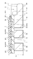
図1乃至図3は、本発明による実施形態1の配線板の概略構成を示す模式図であり、図1は半導体装置の平面図、図2は図1のA−A’線での断面図、図3は図2の部分拡大図である。
【0038】
図1乃至図3において、1は絶縁体(絶縁性接着材料)、2は配線、2Aはビア、2Bは配線のインナーリード部、2Cは配線の外部端子部(ランド)、201は第1導体膜、202は第2導体膜、3は導体板(放熱板)、4は半導体チップを実装する領域(チップ実装領域)、5は凹部空間(デバイスホール)、6は接合材、7は保護膜である。
【0039】
本実施形態1の配線板は、図1乃至図3に示すように、絶縁体1の第1主面に配線(導体パターン)2が設けられており、前記絶縁体1の第1主面の裏面(以下、第2主面と称する)には、導体板3が設けられている。このとき、前記絶縁体1には、例えば、イミド系樹脂などの高耐熱性接着剤を用いる。以下、前記絶縁体1のことを、絶縁性接着材料と称する。
【0040】
また、本実施形態1の配線板は、半導体チップを実装して半導体装置を製造するときに用いる配線板であり、前記絶縁性接着材料1は、半導体チップが実装される領域4が開口している。以下、前記半導体チップが実装される領域4を、チップ実装領域と称する。
【0041】
また、前記導体板3は、前記絶縁性接着材料1のチップ実装領域4の開口部1Aをふさぐように設けられており、且つ前記絶縁性接着材料1のチップ実装領域4の開口部1Aと重なる領域に凹部(座ぐり)3Aが設けられている。このとき、前記半導体チップは、前記導体板3の凹部3Aの底面に接着される。すなわち、本実施形態1の配線板を用いて半導体装置を製造するときには、前記絶縁性接着材料1のチップ実装領域4の開口部1A及び前記導体板3の凹部3Aで構成される凹部空間5の内部に半導体チップを収容することになる。以下、前記絶縁性接着材料1のチップ実装領域4の開口部1A及び前記導体板3の凹部3Aで構成される凹部空間5をデバイスホールと称する。
【0042】
またこのとき、前記導体板3の凹部3Aの深さは、図2に示したような、前記配線2の表面から前記放熱板3の凹部3Aの底面までの距離D1が100μm程度になる深さであるとする。
【0043】
また、前記導体板3は、本実施形態1の配線板を用いて半導体装置を製造したときに、前記半導体チップから発生する熱を外部に放出しやすくするために設けている。そのため、以下、前記導体板3を放熱板と称する。
【0044】
また、前記放熱板3は、図2に示したように、前記絶縁性接着材料1の第2主面側に、全面的に設けられており、前記配線2のうち、例えば、グラウンド電位(接地電位)や電源電位などの、特定の電位の配線と電気的に接続されているものとする。このとき、前記配線2は、例えば、図2に示したように、前記絶縁性接着材料1に設けられた開口部(ブラインドビアホール)1Bの内部で前記放熱板3と接続されている。以下、前記配線2の、前記ブラインドビアホール1Bの内部に設けられた部分をビア2Aと称する。
【0045】
またこのとき、前記配線2は、例えば、図3に示したように、第1導体膜201上に第2導体膜202が積層された状態になっており、前記絶縁体1のブラインドビアホール1B内には、前記第2導体膜202が埋め込まれた状態になっている。つまり、前記ビア2Aは前記第2導体膜202でなる。
【0046】
また、前記配線2は、例えば、半導体装置を製造したときに、半導体チップの外部電極と接続される部分(インナーリード部)2Bや、外部接続端子を形成する領域(外部端子部)2Cの表面に、金めっきなどの接合材6が設けられている。また、前記配線2の、前記接合材6が設けられた領域以外の領域の表面には、はんだ保護膜(ソルダレジスト)などの保護膜7が設けられている。
【0047】
本実施形態1の配線板では、前記絶縁性接着材料1の厚さは10μmから75μm程度にすることができる。また、前記放熱板3には、例えば、厚さが75μmから250μmの銅板を用いることができる。また、前記配線2は、前記第1導体膜201の厚さが12μm程度であり、前記第2導体膜202の厚さが15μm程度である。このとき、前記絶縁性接着材料1の厚さを25μm、前記放熱板3の厚さを75μmとすれば、本実施形態1の配線板の厚さT1は、前記保護膜7の厚さを考慮しても、140μmから150μmとなる。
【0048】
図4乃至図6は、本実施形態1の配線板の製造方法を説明するための模式図であり、図4(a)は積層体を形成する工程の断面図、図4(b)はブラインドビアホールを形成する工程の断面図、図5(a)は第2導体膜(ビア)を形成する工程の断面図、図5(b)は配線を形成する工程の断面図、図6はデバイスホールを形成する工程の断面図である。
【0049】
以下、図4乃至図6に沿って、本実施形態1の配線板の製造方法について説明する。
【0050】
まず、図4(a)に示すように、絶縁性接着材料(絶縁体)1の第1主面に第1導体膜201が張り合わされ、前記絶縁性接着材料1の第2主面に導体板3が張り合わされた積層体を形成する。このとき、前記絶縁性接着材料1には、例えば、イミド系樹脂のような耐熱性の高い樹脂系の絶縁性接着剤を用い、前記第1導体膜201の表面、あるいは前記導体膜3の表面に形成(塗布)しておき、熱プレスなどで接着する。またこのとき、前記絶縁性接着材料1は、接着後の厚さが、例えば、50μm程度になるように形成する。
【0051】
また、前記第1導体膜201には、例えば、厚さが12μm程度の銅箔を用いる。また、前記導体板3には、例えば、厚さが100μm程度の銅板を用いる。
【0052】
また、前記絶縁性接着材料1には、例えば、フィルム状の絶縁体(絶縁フィルム)の両面に接着剤を形成した接着フィルムを用いることもできる。このとき、前記絶縁フィルムには、例えば、厚さが25μm程度のポリイミド系樹脂などの耐熱性の高い絶縁樹脂フィルムを用い、前記接着剤には、例えば、イミド系樹脂を用いる。また、前記接着剤は、例えば、厚さが12μm程度になるように形成する。
【0053】
前記絶縁性接着材料1として、前記接着フィルムを用いた場合、中央の前記フィルム状の絶縁板がコア(芯)の役割をするため、熱プレスによる接着後の前記積層体の厚さのばらつきを低減することができる。
【0054】
次に、図4(b)に示すように、前記積層体のあらかじめ定められた位置に、前記第1導体膜201側から、前記第1導体膜201及び前記絶縁性接着材料1を貫通して前記導体板3に達する開口部(ブラインドビアホール)1Bを形成する。前記ブラインドビアホール1Bは、例えば、炭酸ガスレーザなどのレーザ光を照射して形成する。
【0055】
次に、前記第1導体膜201の表面及び前記ブラインドビアホール1B内に第2導体膜202を形成し、図5(a)に示すように、前記絶縁性接着材料1の第1主面側の配線形成用の導体膜2’と前記絶縁性接着材料1の第2主面側の導体板3をビア2Aで電気的に接続する。前記第2導体膜202は、例えば、電気銅めっきで形成する。このとき、前記第2導体膜202は、前記ブラインドビアホール1B内に選択的に形成されるようにし、前記ブラインドビアホール1Bの内部に前記導体膜202が充填されたときに、前記第1導体膜201上に形成される第2導体膜202の厚さが15μm程度になるようにする。
【0056】
次に、配線形成用の導体膜2’、すなわち、前記第1導体膜201及びその表面の第2導体膜202の不要な部分を除去し、図5(b)に示すように、配線2を形成する。前記配線2は、一般に、ウェットエッチングにより形成するので、エッチングを行う際には、前記導体板3の表面にレジスト(エッチングレジスト)を形成してから行い、エッチング後に前記エッチングレジストを除去する。
【0057】
次に、図6に示すように、半導体装置を製造するときに半導体チップを収容する凹部空間であるデバイスホール5を形成する。前記デバイスホール5は、前記絶縁性接着材料1のチップ実装領域4を開口するとともに、前記導体板3の、前記絶縁性接着材料1のチップ実装領域4の開口部1Aと重なる領域に凹部3Aを形成する。このとき、前記絶縁性接着材料1の開口部1A及び前記導体板3の凹部3Aは、例えば、ルータを用いた座ぐり加工(spot facing)により形成する。また、前記導体板3の凹部3Aの深さは、例えば、前記配線2の表面から前記凹部3Aの底面までの距離が100μm程度になるようにする。
【0058】
その後、前記配線2の表面に、図2及び図3に示したように、接合材6及びはんだ保護膜などの保護膜7を形成すると、本実施形態1の配線板が得られる。前記接合材6及び前記保護膜7は、例えば、前記配線2のインナーリード部2A及び前記外部端子部2Bにマスクをして前記保護膜7を形成した後、前記マスクを除去して、前記配線2の露出面に、金めっきなどの接合材6を形成する。
【0059】
図7及び図8は、本実施形態1の配線板を用いた半導体装置の製造方法を説明するための模式図であり、図7は半導体チップを実装する工程の断面図、図8は半導体チップを封止して外部接続端子を形成する工程の断面図である。なお、図7及び図8の断面図は、図2と同じ断面で見たときの図である。
【0060】
本実施形態1の配線板を用いて半導体装置を製造するときには、図7に示したように、前記デバイスホール5の底面、すなわち、前記放熱板3の凹部3Aの底面に、例えば、銀ペーストなどの接着剤8を用いて半導体チップ9を接着し、前記配線2のインナーリード部2Bと前記半導体チップ9の外部電極901をボンディングワイヤ10で電気的に接続する。
【0061】
次に、図8に示すように、前記半導体チップ9及び前記ボンディングワイヤ10による接続部を絶縁樹脂(モールド樹脂)11で封止し、前記配線2の外部端子部2Cにボール状の外部接続端子12を形成する。
【0062】
本実施形態1の配線板では、前記絶縁性接着材料(絶縁体)1の厚さを50μm程度、前記放熱板3の厚さを100μmとしているので、前記配線板の厚さは180μmから190μm程度になる。また、本実施形態1の配線板を用いた半導体装置では、前記半導体チップ9を実装する面と、前記外部接続端子12を形成する面が同じ面であるため、前記配線板に実装した半導体チップ9を封止する絶縁樹脂11が、前記配線板から突出(隆起)していても、その高さは無視できる。すなわち、本実施形態1の配線板を用いた半導体装置の厚さT2は、前記配線板の厚さT1と前記ボール状の外部接続端子12の高さ(直径)で決まる。そのため、前記ボール状の外部接続端子12を形成するときに、例えば、直径が650μm程度のはんだボールを用いたとすると、本実施形態1の配線板を用いた半導体装置の厚さT2は、820μmから830μm程度にすることができる。
【0063】
以上説明したように、本実施形態1の配線板の製造方法によれば、導体板(放熱板)3の表面に、絶縁性接着材料1で第1導体膜201を接着した積層体を用いるので、接着剤を用いて各材料を接着する工程は、前記導体板3の表面に前記第1導体膜201を接着する工程のみである。すなわち、本実施形態1の配線板の製造方法を用いることにより、例えば、従来の前記非特許文献1に記載された半導体装置に用いる配線板の製造方法と比べて、製造工程を減らすとともに、材料費を少なくすることができる。そのため、配線板の製造コストを低減することができる。
【0064】
また、前記絶縁性接着材料1を用いて接着する導体の厚さを変えて、厚いほうの導体、すなわち、前記導体板3を放熱板として用いることにより、放熱板を有する配線板を容易に製造することができる。
【0065】
また、本実施形態1の配線板は、前記絶縁性接着材料1の厚さを50μm程度、前記導体板(放熱板)3の厚さを100μmにすることができるので、本実施形態1の配線板を用いたBGA型の半導体装置の厚さT2を1mm以下にすることができる。そのため、例えば、従来の前記非特許文献1や前記特許文献1に記載された半導体装置に比べて、半導体装置の薄型化が容易になる。
【0066】
また、本実施形態1の配線板では、前記絶縁性接着材料1の厚さを50μm程度としたが、これに限らず、前記絶縁性接着材料1の厚さは、10μmから75μm程度にすることができる。また、前記導体板(放熱板)3も、厚さが100μmのものに限らず、75μmから250μm程度のものを用いることができる。そのため、前記絶縁性接着材料1の厚さを25μmとし、前記導体板(放熱板)3の厚さを75μmとすれば、半導体装置の厚さT2をさらに薄くすることができる。
【0067】
また、本実施形態1の配線板のように、前記配線2のうち、グラウンド電位(接地電位)などの等電位の配線と前記放熱板3を前記ビア2Aで電気的に接続することにより、前記放熱板3をグラウンド層(面)にすることができる。そのため、前記配線板に、マイクロストリップと呼ばれる形態の伝送路を設けることができ、高周波信号(電流)を伝送するときのクロストークノイズ、伝送ロスや遅延を低減することができる。
【0068】
また、前記絶縁性接着材料1として、フィルム状の絶縁板の両面に絶縁性の接着剤が形成された3層構造の接着フィルムを用いると、中央の前記フィルム状の絶縁板がコア(芯)の役割をするため、接着後の、前記導体膜及び前記絶縁性接着材料、ならびに前記導体板からなる積層体の厚さのばらつきを低減することができる。そのため、前記配線板のばらつきを低減することができ、前記半導体装置の厚さのばらつきを低減することができる。
【0069】
(実施形態2)
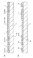
図9乃至図11は、本発明による実施形態2の配線板の概略構成を示す模式図であり、図9は配線板の平面図、図10は図9のB−B’線での断面図、図11は図10の部分拡大断面図である。
【0070】
図9乃至図11において、1は絶縁体(絶縁性接着材料)、2は配線、2Aはビア、2Bは配線のインナーリード部、201は第1導体膜、202は第2導体膜、3は導体板(放熱板)、6Aは第1接合材、6Bは第2接合材、13は外部接続端子(ランド)である。
【0071】
本実施形態2の配線板は、図9乃至図11に示すように、絶縁体1の第1主面に配線(導体パターン)2が設けられており、前記絶縁体1の第1主面の裏面(以下、第2主面と称する)には、導体板3が設けられている。このとき、前記絶縁体1には、例えば、イミド系樹脂などの高耐熱性接着剤を用いる。以下、前記絶縁体1のことを、絶縁性接着材料と称する。
【0072】
また、本実施形態2の配線板は、半導体チップを実装して半導体装置を製造するときに用いる配線板であり、前記絶縁性接着材料1は、半導体チップが実装される領域(チップ実装領域)4が開口している。
【0073】
また、前記導体板3は、前記絶縁性接着材料1のチップ実装領域4の開口部1Aを覆うように設けられており、且つ前記絶縁性接着材料1のチップ実装領域4の開口部1Aと重なる領域に凹部(座ぐり)3Aが設けられている。このとき、前記半導体チップは、前記導体板3の凹部3Aの底面に接着される。すなわち、本実施例2の配線板を用いて半導体装置を製造するときには、前記絶縁性接着材料1の開口部1A及び前記導体板3の凹部3Aで構成される凹部空間(デバイスホール)5の内部に半導体チップを収容することになる。
【0074】
またこのとき、前記導体板3の凹部3Aの深さは、前記配線2の表面から前記放熱板3の凹部3Aの底面までの距離D2が100μm程度になる深さであるとする。
【0075】
また、前記導体板3は、本実施形態2の配線板を用いて半導体装置を製造したときに、前記半導体チップから発生する熱を外部に放出しやすくするために設けている。そのため、以下、前記導体板3を放熱板と称する。
【0076】
また、本実施形態2の配線板では、前記絶縁性接着材料1の第2主面の、前記放熱板3の外側の領域に、前記放熱板3とは電気的に分離しており、且つ前記配線2と電気的に接続された外部接続端子(ランド)13が設けられている。また、前記放熱板3は、図10に示したように、前記配線2のうち、例えば、グラウンド電位(接地電位)や電源電位などの、特定の電位の配線と電気的に接続されているものとする。このとき、前記配線2と前記ランド13、及び前記配線2と前記放熱板3は、前記絶縁性接着材料1の開口部(ブラインドビアホール)1Bの内部に設けられた導体(ビア)2Aにより電気的に接続されている。
【0077】
またこのとき、前記配線2は、例えば、図11に示したように、第1導体膜201上に第2導体膜202が積層された状態になっており、前記絶縁性接着材料1のブラインドビアホール1B内には、前記第2導体膜202が埋め込まれた状態になっている。つまり、前記ビア2Aは前記第2導体膜202でなる。
【0078】
また、前記配線2は、例えば、半導体装置を製造したときに、半導体チップの外部電極と接続される領域(インナーリード部)2Bの表面に、金めっきなどの第1接合材6Aが設けられている。また、前記配線2の、前記第1接合材6Aが設けられた領域以外の領域の表面には、はんだ保護膜(ソルダレジスト)などの保護膜7が設けられている。また、前記外部接続端子13及び前記放熱板3の表面には、例えば、金めっき、錫鉛合金めっき、錫銀合金めっきなどの第2接合材6Bが設けられている。
【0079】
また、本実施形態2の配線板でも、前記絶縁性接着材料1の厚さは10μmから75μm程度にすることができる。また、前記放熱板3及び前記外部接続端子13には、例えば、厚さが75μmから250μmの銅板を用いることができる。また、前記配線2は、前記第1導体膜201の厚さが12μm程度であり、前記第2導体膜202の厚さが15μm程度である。このとき、前記絶縁性接着材料1の厚さを25μm、前記放熱板3の厚さを75μmとすれば、本実施形態2の配線板の厚さT3は、前記保護膜7や前記第2接合材6Bの厚さを考慮しても、140μmから150μmとなる。
【0080】
図12乃至図14は、本実施形態2の配線板の製造方法を説明するための模式図であり、図12(a)は積層体を形成する工程の断面図、図12(b)はブラインドビアホールを形成する工程の断面図、図13(a)は第2導体膜(ビア)を形成する工程の断面図、図13(b)は配線を形成する工程の断面図、図14(a)は放熱板及び外部接続端子を形成する工程の断面図、図14(b)はデバイスホールを形成する工程の断面図である。
【0081】
以下、図12乃至図14に沿って、本実施形態2の配線板の製造方法について説明する。なお、前記実施形態1で説明した手順と同じ部分については、詳細な説明を省略する。
【0082】
本実施形態2の配線板を製造するときには、まず、図12(a)に示すように、導体板3’の一表面に、絶縁性接着材料1を用いて銅箔などの第1導体膜201を接着した積層板を形成する。前記積層板は、前記実施形態1で説明したような方法で形成する。
【0083】
次に、図12(b)に示すように、前記第1導体膜201及び前記絶縁性接着材料1を貫通して前記導体板3’に達する開口部(ブラインドビアホール)1Bを形成する。その後、例えば、電気銅めっきにより、前記ブラインドビアホール1Bの内部及び前記第1導体膜201の表面に第2導体膜202を形成して、図13(a)に示すように、配線形成用の導体膜2’及び前記配線形成用の導体膜2’と前記導体板3を電気的に接続する導体(ビア)2Aを形成する。
【0084】
次に、図13(b)に示すように、前記配線形成用の導体膜2’、すなわち前記第1導体膜201とその表面の第2導体膜202の不要な部分を除去して配線2を形成する。前記配線2は、一般に、ウェットエッチングにより形成するので、前記エッチングを行う前に、前記導体板3’の表面に溶解を防ぐレジスト(エッチングレジスト)を形成し、エッチング後に前記エッチングレジストを除去する。
【0085】
次に、図14(a)に示すように、前記導体板3’の不要な部分を除去して、前記放熱板3及び前記外部接続端子13を形成する。前記放熱板3及び前記外部接続端子13を形成するときも、ウェットエッチングで行うのが一般的であるため、エッチングを行う前に、前記配線2上にレジスト(エッチングレジスト)を形成し、エッチング後に前記エッチングレジストを除去する。
【0086】
次に、図14(b)に示すように、半導体装置を製造するときに半導体チップを収容する凹部空間であるデバイスホール5を形成する。前記デバイスホール5は、前記絶縁性接着材料1のチップ実装領域4を開口するとともに、前記放熱板3の、前記絶縁性接着材料1のチップ実装領域4の開口部1Aと重なる領域に凹部3Aを形成する。このとき、前記絶縁性接着材料1の開口部1A及び前記導体板3の凹部3Aは、例えば、ルータを用いた座ぐり加工(spot facing)により形成する。また、前記導体板3の凹部3Aの深さは、例えば、前記配線2の表面から前記凹部3Aの底面までの距離が100μm程度になるようにする。
【0087】
その後、図10及び図11に示したように、前記配線2の表面に第1接合材6A及びはんだ保護膜などの保護膜7を形成し、前記放熱板3及び前記外部接続端子13の表面に、第2接合材6Bを形成すると、本実施形態2の配線板が得られる。このとき、前記第1接合材4Aと前記第2接合材4Bは、同種の材料を用いて形成してもよいし、異なる種類の材料を用いて形成してもよい。
【0088】
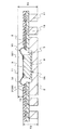
図15は、本実施形態2の配線板を用いた半導体装置の概略構成を示す模式図である。
【0089】
本実施形態2の配線板を用いて半導体装置を製造するときも、図15に示すように、前記デバイスホール5の底面、すなわち、前記放熱板3の凹部3Aの底面に、銀ペーストなどの接着剤8を用いて半導体チップ9を接着し、前記配線2のインナーリード部2Bと前記半導体チップ9の外部電極901をボンディングワイヤ10で電気的に接続する。その後、前記半導体チップ9及び前記ボンディングワイヤ10による接続部を絶縁樹脂(モールド樹脂)11で封止する。
【0090】
また、本実施形態2の配線板を用いた半導体装置は、LGA(Land Grid Array)と呼ばれる形態の半導体装置であり、実装基板などに実装するときには、前記外部接続端子13を、前記実装基板の配線(端子)と直接接続することができる。このとき、前記外部接続端子13は、前記放熱板3と同じ材料、すなわち、導体板を用いているため、表面の平坦性が高い。そのため、従来のLGA型の半導体装置に比べて、前記半導体装置を実装するときの実装性が向上する。
【0091】
また、本実施形態2の配線板を用いた半導体装置の場合、前記半導体チップ9を実装する面の裏面に、前記外部接続端子13が設けられている。そのため、本実施形態2の配線板を用いた半導体装置の厚さT4は、図15に示したように、前記配線板の厚さT3と、前記半導体チップ9が実装された領域の前記絶縁樹脂(モールド樹脂)11の突出分(隆起分)の高さT5の和となる。このとき、前記絶縁性接着材料1の厚さが50μm程度、前記放熱板3の厚さが100μmだとすると、前記配線板の厚さT3は、180μmから190μm程度である。またこのとき、前記デバイスホール5の深さは100μm程度であるので、厚さが100μm程度の半導体チップ9を実装した場合、前記半導体チップ9は、ほぼ全体が前記デバイスホール5の内部に収容される。そのため、前記樹脂材料11の、前記配線板から突出(隆起)した部分の高さT5は100μmから120μm程度にすることができ、半導体装置の厚さT4を300μm程度にすることができる。
【0092】
以上説明したように、本実施形態2の配線板の製造方法によれば、前記実施形態1の配線板の製造方法と同様に、接着剤を用いて各材料を接着する工程は、前記導体板3の表面に前記第1導体膜201を接着する工程のみである。そのため、例えば、従来のLGA型の半導体装置に用いられる配線板(両面配線板)の製造方法と比べて、製造工程の増加や、材料費の増加を防ぐことができる。また、本実施形態2の配線板の製造方法では、前記デバイスホール5を形成する工程を除けば、前記従来の両面配線板と同じ工程数で前記放熱板3も形成することができる。そのため、前記放熱板3が設けられた配線板を容易に製造することができる。
【0093】
また、本実施形態2の配線板は、前記絶縁性接着材料1の厚さを50μm程度、前記導体板(放熱板)3の厚さを100μmにすることができるので、本実施形態2の配線板を用いたLGA型の半導体装置の厚さT4を1mm以下にすることができる。そのため、例えば、従来のLGA型の半導体装置に比べて、半導体装置の薄型化が容易になる。
【0094】
また、本実施形態2の配線板では、前記絶縁性接着材料1の厚さを50μm程度としたが、これに限らず、前記絶縁性接着材料1の厚さは、10μmから75μm程度にすることができる。また、前記導体板(放熱板)3も、厚さが100μmのものに限らず、75μmから250μm程度のものを用いることができる。そのため、前記絶縁性接着材料1の厚さを10μmとし、前記導体板(放熱板)3の厚さを75μmとすれば、半導体装置の厚さT4をさらに薄くすることができる。
【0095】
また、本実施形態2の配線板のように、前記配線2のうち、グラウンド電位(接地電位)などの等電位の配線と前記放熱板3をビア2Aにより電気的に接続することにより、前記放熱板3をグラウンド層(面)にすることができる。そのため、前記配線板に、マイクロストリップと呼ばれる形態の伝送路を設けることができ、高周波信号(電流)を伝送するときのクロストークノイズ、伝送ロスや遅延を低減することができる。
【0096】
なお、前記実施形態2の配線板の製造方法では、前記配線2を形成した後、前記放熱板3及び前記外部接続端子13を形成したが、これに限らず、前記放熱板3及び前記外部接続端子13を形成した後、前記配線2を形成してもよいことは言うまでもない。
【0097】
また、前記絶縁性接着材料1として、フィルム状の絶縁板の両面に絶縁性の接着剤が形成された3層構造の接着フィルムを用いると、中央の前記フィルム状の絶縁板がコア(芯)の役割をするため、接着後の、前記導体膜及び前記絶縁性接着材料、ならびに前記導体板からなる積層体の厚さのばらつきを低減することができる。そのため、前記配線板のばらつきを低減することができ、前記半導体装置の厚さのばらつきを低減することができる。
【0098】
以上、本発明を、前記実施形態に基づき具体的に説明したが、本発明は、前記実施形態に限定されるものではなく、その要旨を逸脱しない範囲において、種々変更可能であることはもちろんである。
【0099】
例えば、前記実施形態1及び前記実施形態2の配線板では、前記配線2と前記放熱板3、あるいは前記配線2と前記外部接続端子13は、ビア2A、すなわち、前記絶縁性接着材料(絶縁体)1に形成したブラインドビアホール1B内に充填された第2導体膜202により電気的に接続したが、これに限らず、めっきスルーホール(plated through hole)により電気的に接続してもよい。
【0100】
また、前記実施形態1及び前記実施形態2の配線板では、前記放熱板3をグラウンド層(面)として用いる例を示したが、例えば、高周波信号(電流)を扱わない場合などは、前記配線2と前記放熱板3を電気的に接続しなくてもよい。
【0101】
また、例えば、前記実施形態1及び前記実施形態2では、前記絶縁性接着材料1の第1主面に前記配線2を設け、前記絶縁性接着材料1の第2主面に前記放熱板3を設けた配線板、すなわち、配線層が2層の配線板(両面配線板)を例に挙げて説明したが、これに限らず、配線層が3層以上の多層配線板に、本発明を適用することもできる。前記多層配線板に適用する場合は、例えば、前記実施形態1で説明した手順に沿って前記配線2を形成した後、前記配線2が形成された面(第1主面)に、前記絶縁性接着材料1を用いて導体膜を接着し、前記導体膜を用いて新たな配線を形成すればよい。
【0102】
【発明の効果】
本願において開示される発明のうち、代表的なものによって得られる効果を簡単に説明すれば、以下の通りである。
【0103】
(1)放熱板を有する配線板の製造コストを低減することができる。
【0104】
(2)放熱板を有する配線板を用いた半導体装置の薄型化が可能である。
【図面の簡単な説明】
【図1】本発明による実施形態1の配線板の概略構成を示す模式図であり、配線板の平面図である。
【図2】本実施形態1の配線板の概略構成を示す模式図であり、図1のA−A’線での断面図である。
【図3】本実施形態1の配線板の概略構成を示す模式図であり、図2の部分拡大断面図である。
【図4】本実施形態1の配線板の製造方法を説明するための模式図であり、図4(a)は積層体を形成する工程の断面図、図4(b)はブラインドビアホールを形成する工程の断面図である。
【図5】本実施形態1の配線板の製造方法を説明するための模式図であり、図5(a)は第2導体膜(ビア)を形成する工程の断面図、図5(b)は配線を形成する工程の断面図である。
【図6】本実施形態1の配線板の製造方法を説明するための模式図であり、デバイスホールを形成する工程の断面図である。
【図7】本実施形態1の配線板を用いた半導体装置の製造方法を説明するための模式図であり、半導体チップを実装する工程の断面図である。
【図8】本実施形態1の配線板を用いた半導体装置の製造方法を説明するための模式図であり、半導体チップを封止して外部接続端子を形成する工程の断面図である。
【図9】本発明による実施形態2の配線板の概略構成を示す模式図であり、配線板の平面図である。
【図10】本実施形態2の配線板の概略構成を示す模式図であり、図9のB−B’線での断面図である。
【図11】本実施形態2の配線板の概略構成を示す模式図であり、図10の部分拡大断面図である。
【図12】本実施形態2の配線板の製造方法を説明するための模式図であり、図12(a)は積層体を形成する工程の断面図、図12(b)はブラインドビアホールを形成する工程の断面図である。
【図13】本実施形態2の配線板の製造方法を説明するための模式図であり、図13(a)は第2導体膜(ビア)を形成する工程の断面図、図13(b)は配線を形成する工程の断面図である。
【図14】本実施形態2の配線板の製造方法を説明するための模式図であり、図14(a)は放熱板及び外部接続端子を形成する工程の断面図、図14(b)はデバイスホールを形成する工程の断面図である。
【図15】本実施形態2の配線板を用いた半導体装置の概略構成を示す模式断面図である。
【図16】従来のTBGA型の半導体装置の概略構成を示す模式断面図である。
【符号の説明】
1 絶縁体(絶縁性接着材料)
1A チップ実装領域の開口部
1B ブラインドビアホール
2 配線
2A ビア
2B 配線のインナーリード部
2C 配線の外部端子部
201 第1導体膜
202 第2導体膜
3 導体板(放熱板)
3A 放熱板の凹部の底面
3’ 導体板
4 半導体チップを実装する領域
5 凹部空間(デバイスホール)
6 接合材
6A 第1接合材
6B 第2接合材
7 保護膜
8 接着剤
9 半導体チップ
901 半導体チップの外部電極
10 ボンディングワイヤ
11 絶縁樹脂(モールド樹脂)
12 ボール状の外部接続端子
13 外部接続端子(ランド)
14 絶縁基板
15 絶縁性接着剤[0001]
TECHNICAL FIELD OF THE INVENTION
The present invention relates to a method for manufacturing a wiring board, a wiring board, and a semiconductor device, and more particularly to a technique that is effective when applied to a method for manufacturing a wiring board having a heat dissipation conductor plate (hereinafter, referred to as a heat dissipation plate). is there.
[0002]
[Prior art]
2. Description of the Related Art Conventionally, as a semiconductor device having a semiconductor chip mounted on a wiring board, there is a semiconductor device provided with a heat radiating plate for releasing heat generated in the semiconductor chip to the outside. As the semiconductor device provided with the heat sink, there is, for example, a semiconductor device called a TBGA (Tape Ball Grid Array).
[0003]
In a semiconductor device called TBGA, for example, a wiring board in which wiring (conductor pattern) is provided on the surface of an insulating substrate, a heat sink bonded to the wiring board, and a wiring board and the heat sink are provided. There is a semiconductor device including a semiconductor chip housed in a recessed portion (for example, see Non-Patent Document 1).
[0004]
In the TBGA type semiconductor device disclosed in
[0005]
When manufacturing the TBGA type semiconductor device disclosed in Non-Patent
[0006]
In the wiring board forming step, first, a conductive film is formed on a first main surface and a second main surface of a tape-shaped
[0007]
In the semiconductor chip mounting step, first, the
[0008]
Further, in addition to the semiconductor device shown in Non-Patent
[0009]
[Non-patent document 1]
Tatsuya Otaka, Hiroshi Sugimoto, Tomoo Omori, Yukio Suzuki, "TBGA (Tape Ball Grid Array) for image processing and communication system LSI mounting", Hitachi Cable, Hitachi Cable, Ltd., January 2000, No. 19, p. 79-84
[Patent Document 1]
JP-A-08-306820 (
[0010]
[Problems to be solved by the invention]
However, among the conventional techniques, in a manufacturing process of a wiring board used for the semiconductor device of the mode described in Non-Patent
[0011]
In the TBGA type semiconductor device described in Non-Patent
[0012]
In the case of the semiconductor device of the form (MBGA type) described in
[0013]
An object of the present invention is to provide a technique capable of reducing the manufacturing cost of a wiring board having a heat sink.
[0014]
Another object of the present invention is to provide a technique capable of reducing the thickness of a semiconductor device using a wiring board having a heat sink.
[0015]
The above and other objects and novel features of the present invention will become apparent from the description of the present specification and the accompanying drawings.
[0016]
[Means for Solving the Problems]
The outline of the invention disclosed in the present application is as follows.
[0017]
(1) A method for manufacturing a wiring board, wherein a wiring (conductor pattern) is formed on a surface of the insulator, or on the surface and inside thereof, and a conductor plate for heat dissipation is formed on one surface of the insulator. A conductor film is adhered to one surface of the board using an insulating adhesive material, and after removing unnecessary portions of the conductor film to form the wiring, a predetermined region of the insulating adhesive material is opened. And a method of manufacturing a wiring board in which a recess is formed in a region of the conductor plate on the side of the bonding surface with the insulating adhesive material, which overlaps with the opening region of the insulating adhesive material.
[0018]
According to the means (1), the wiring is formed by using the conductor film adhered to the conductor plate for heat dissipation with the insulating adhesive material. The manufacturing process and the material cost can be reduced as compared with the method for manufacturing a wiring board. Therefore, the manufacturing cost of the wiring board can be reduced.
[0019]
In the means (1), the conductive film and the conductive plate may be electrically connected at a predetermined position before the wiring is formed. In this case, when an unnecessary portion of the conductor film is removed to form a wiring, the wiring having a specific potential such as a ground potential (ground potential) or a power supply potential is connected to the wiring for the heat dissipation. If the conductor plate is connected, the conductor plate for heat dissipation can be used as a ground layer (surface), and a wiring board having a transmission path in the form of a microstrip can be easily manufactured.
[0020]
When the means (1) is used, before forming the wiring or after forming the wiring, an unnecessary portion of the conductor plate is removed to cover the opening of the insulating adhesive material. A heat dissipation conductor plate and an external connection terminal (land) electrically separated from the conductor plate may be formed. At this time, the external connection terminal has the same thickness as the heat dissipation conductor plate, and is sufficiently thicker than the thickness of the wiring. Further, since the external connection terminal is made of the same material as the heat dissipation conductor plate, the surface of the external connection terminal has higher flatness than a terminal (wiring) formed by plating or the like. Therefore, when a semiconductor device is manufactured using the wiring board, the connectivity between the external connection terminal and the wiring (terminal) of another wiring board (mounting board) can be improved.
[0021]
In the means (1), it is preferable to use, for example, a high heat-resistant adhesive such as an imide-based resin as the insulating adhesive material. At this time, the high heat-resistant adhesive is formed (applied) on the surface of the conductor film or the surface of the conductor plate, for example, and adhered by hot pressing.
[0022]
Further, as the insulating adhesive material, an adhesive film having a three-layer structure in which an insulating adhesive is formed on both surfaces of a film-shaped insulating plate can be used. In the case of the adhesive film, since the central film-shaped insulating plate serves as a core, the thickness of the conductor film, the insulating adhesive material, and the laminate made of the conductive plate after bonding are determined. Can be reduced.
[0023]
(2) Wiring (conductor pattern) is provided on the surface of the insulator, or on the surface and inside thereof, and a conductor plate for heat dissipation is provided on one surface of the insulator, and the insulator has a predetermined area. The heat dissipation conductor plate is provided so as to cover the opening of the insulator, and a concave portion is provided on an adhesive surface side of the insulator with a region overlapping the opening of the insulator. Wherein the wiring is a wiring board adhered on one surface of the heat-dissipating conductor plate with an insulating adhesive material.
[0024]
According to the means (2), since the wiring is adhered on one surface of the heat dissipation conductor plate, a conventional wiring is formed on the surface of the insulating substrate, and then the adhesive is formed using an adhesive. The thickness can be reduced as compared with a wiring board in which a heat sink is bonded to the insulating substrate.
[0025]
In the means (2), for example, the heat-dissipating conductor plate is electrically connected to a predetermined wiring so that, for example, the heat-dissipating conductor plate is a ground layer (surface). Thus, a wiring board having a transmission path in a form called a microstrip can be obtained. Therefore, signal deterioration, transmission loss, and delay when transmitting a high-frequency signal (current) can be reduced.
[0026]
In the means of the above (2), the surface of the insulating adhesive material provided with the heat dissipation conductor plate is electrically separated from the heat dissipation conductor plate and electrically connected to the wiring. A connected external connection terminal (land) may be provided. At this time, the semiconductor device manufactured using the wiring board can be in a form called LGA (Land Grid Array).
[0027]
In addition, when a three-layer adhesive film in which an insulating adhesive is formed on both sides of a film-shaped insulating plate is used as the insulating adhesive material, the film-shaped insulating plate at the center has a core (core). Since it plays a role, variations in the thickness of the wiring board can be reduced.
[0028]
(3) A wiring board in which wiring (conductor pattern) is provided on the surface of the insulator or on the surface and inside thereof, and a conductor plate for heat dissipation is provided on one surface of the insulator, and the wiring board is provided on the wiring board. A semiconductor chip, and a bonding wire for electrically connecting a wiring of the wiring board and an external electrode of the semiconductor chip, wherein the insulator has an opening in a predetermined region, and the heat dissipation conductor The plate is provided so as to cover the opening of the insulator, and a concave portion is provided in a region overlapping the opening of the insulator on the side of the bonding surface with the insulator, and the semiconductor chip includes: A semiconductor device adhered to a bottom surface of the concave portion provided on the heat dissipation conductor plate, wherein the wiring is adhered on one surface of the heat dissipation conductor plate with an insulating adhesive material. It is a semiconductor device.
[0029]
According to the means (3), the wiring is adhered to one surface of the heat dissipation conductor plate, and the semiconductor chip is adhered to the bottom surface of the concave portion of the heat dissipation conductor plate. Therefore, the thickness can be reduced as compared with a conventional semiconductor device described in, for example,
[0030]
In the means (3), the heat-dissipating conductor plate is electrically connected to a predetermined wiring, so that the heat-dissipating conductor plate is, for example, a ground layer (surface). Can be. Therefore, signal deterioration, transmission loss, and delay when transmitting a high-frequency signal (current) can be reduced.
[0031]
In the means of the above (3), if a ball-shaped external connection terminal is provided at one end of the wiring, for example, a semiconductor device having the same form as a semiconductor device called a TBGA described in
[0032]
Further, when the ball-shaped external connection terminal is provided at one end of the wiring, the surface on which the semiconductor chip is mounted is the same as the surface on which the ball-shaped external connection terminal is provided. The thickness can be reduced as compared with the semiconductor device of the form called MBGA (Metal BGA) described in No. 1.
[0033]
In the means of the above (3), instead of the ball-shaped external connection terminal, one end of the wiring may be provided on the surface of the insulating adhesive material provided with the heat-dissipating conductor plate. An external connection terminal (land) that is electrically separated from the conductive plate and electrically connected to the wiring may be provided. In this case, the semiconductor device takes a form called LGA. At this time, by providing the semiconductor chip in the concave portion of the heat dissipation conductor plate, the thickness can be reduced as compared with the conventional LGA type semiconductor device.
[0034]
In addition, when a three-layer adhesive film in which an insulating adhesive is formed on both sides of a film-shaped insulating plate is used as the insulating adhesive material, the film-shaped insulating plate at the center has a core (core). Since it plays a role, the variation in the thickness of the wiring board can be reduced, and the variation in the thickness of the semiconductor device can be reduced.
[0035]
Hereinafter, the present invention will be described in detail with embodiments (examples) with reference to the drawings.
[0036]
In all the drawings for describing the embodiments, components having the same function are denoted by the same reference numerals, and the repeated description thereof will be omitted.
[0037]
BEST MODE FOR CARRYING OUT THE INVENTION
(Embodiment 1)
1 to 3 are schematic diagrams showing a schematic configuration of a wiring board according to a first embodiment of the present invention. FIG. 1 is a plan view of a semiconductor device, and FIG. 2 is a cross-sectional view taken along line AA ′ of FIG. FIG. 3 is a partially enlarged view of FIG.
[0038]
1 to 3, 1 is an insulator (insulating adhesive material), 2 is a wiring, 2A is a via, 2B is an inner lead part of the wiring, 2C is an external terminal part (land) of the wiring, and 201 is a first conductor.
[0039]
As shown in FIGS. 1 to 3, the wiring board according to the first embodiment is provided with a wiring (conductor pattern) 2 on a first main surface of an
[0040]
The wiring board according to the first embodiment is a wiring board used when manufacturing a semiconductor device by mounting a semiconductor chip. The insulating
[0041]
The
[0042]
At this time, the depth of the
[0043]
Further, the
[0044]
Further, as shown in FIG. 2, the
[0045]
At this time, for example, as shown in FIG. 3, the
[0046]
In addition, for example, when the semiconductor device is manufactured, the
[0047]
In the wiring board of the first embodiment, the thickness of the insulating
[0048]
4 to 6 are schematic views for explaining the method of manufacturing the wiring board according to the first embodiment. FIG. 4A is a cross-sectional view of a process for forming a laminate, and FIG. 4B is a blind. FIG. 5A is a cross-sectional view of a step of forming a second conductor film (via), FIG. 5B is a cross-sectional view of a step of forming a wiring, and FIG. 6 is a device hole. FIG. 4 is a cross-sectional view of a step of forming a semiconductor device.
[0049]
Hereinafter, the method of manufacturing the wiring board according to the first embodiment will be described with reference to FIGS.
[0050]
First, as shown in FIG. 4A, a
[0051]
For the first
[0052]
Further, as the insulating
[0053]
When the adhesive film is used as the insulating
[0054]
Next, as shown in FIG. 4B, the
[0055]
Next, a second
[0056]
Next, unnecessary portions of the
[0057]
Next, as shown in FIG. 6, a
[0058]
Thereafter, as shown in FIGS. 2 and 3, a
[0059]
7 and 8 are schematic views for explaining a method of manufacturing a semiconductor device using the wiring board according to the first embodiment. FIG. 7 is a cross-sectional view of a step of mounting a semiconductor chip. FIG. FIG. 4 is a cross-sectional view of a step of forming an external connection terminal by sealing the semiconductor device. Note that the cross-sectional views of FIGS. 7 and 8 are views when viewed in the same cross-section as FIG.
[0060]
When a semiconductor device is manufactured using the wiring board of the first embodiment, as shown in FIG. 7, for example, a silver paste or the like is provided on the bottom surface of the
[0061]
Next, as shown in FIG. 8, a connection portion of the
[0062]
In the wiring board of the first embodiment, the thickness of the insulating adhesive material (insulator) 1 is about 50 μm and the thickness of the
[0063]
As described above, according to the method for manufacturing a wiring board of the first embodiment, the laminate in which the first
[0064]
Also, by changing the thickness of the conductor to be bonded using the insulating
[0065]
Further, in the wiring board of the first embodiment, the thickness of the insulating
[0066]
Further, in the wiring board of the first embodiment, the thickness of the insulating
[0067]
Further, as in the wiring board of the first embodiment, by electrically connecting the wiring of the same potential, such as the ground potential (ground potential), of the
[0068]
When a three-layered adhesive film in which an insulating adhesive is formed on both sides of a film-like insulating plate is used as the insulating
[0069]
(Embodiment 2)
9 to 11 are schematic views illustrating a schematic configuration of a wiring board according to
[0070]
9 to 11,
[0071]
In the wiring board of the second embodiment, as shown in FIGS. 9 to 11, a wiring (conductor pattern) 2 is provided on a first main surface of an
[0072]
The wiring board according to the second embodiment is a wiring board used when manufacturing a semiconductor device by mounting a semiconductor chip, and the insulating
[0073]
The
[0074]
At this time, the depth of the
[0075]
Further, the
[0076]
In the wiring board of the second embodiment, the second main surface of the insulating
[0077]
At this time, for example, as shown in FIG. 11, the
[0078]
The
[0079]
Further, also in the wiring board of the second embodiment, the thickness of the insulating
[0080]
12 to 14 are schematic views for explaining a method of manufacturing a wiring board according to the second embodiment. FIG. 12A is a cross-sectional view of a process for forming a laminate, and FIG. FIG. 13A is a sectional view of a step of forming a second conductive film (via), FIG. 13B is a sectional view of a step of forming a wiring, and FIG. FIG. 14B is a sectional view of a step of forming a heat sink and external connection terminals, and FIG. 14B is a sectional view of a step of forming a device hole.
[0081]
Hereinafter, the method of manufacturing the wiring board according to the second embodiment will be described with reference to FIGS. Note that detailed description of the same steps as those described in the first embodiment will be omitted.
[0082]
When manufacturing the wiring board of the second embodiment, first, as shown in FIG. 12A, a first
[0083]
Next, as shown in FIG. 12B, an opening (blind via hole) 1B penetrating the first
[0084]
Next, as shown in FIG. 13 (b), the
[0085]
Next, as shown in FIG. 14A, unnecessary portions of the
[0086]
Next, as shown in FIG. 14B, a
[0087]
Thereafter, as shown in FIGS. 10 and 11, a
[0088]
FIG. 15 is a schematic diagram illustrating a schematic configuration of a semiconductor device using the wiring board according to the second embodiment.
[0089]
When a semiconductor device is manufactured using the wiring board according to the second embodiment, as shown in FIG. 15, a silver paste or the like is adhered to the bottom of the
[0090]
The semiconductor device using the wiring board according to the second embodiment is a semiconductor device in a form called an LGA (Land Grid Array). When the semiconductor device is mounted on a mounting board or the like, the
[0091]
In the case of the semiconductor device using the wiring board of the second embodiment, the
[0092]
As described above, according to the method for manufacturing a wiring board of the second embodiment, similarly to the method of manufacturing a wiring board of the first embodiment, the step of bonding each material using an adhesive includes the steps of: Only the step of bonding the
[0093]
In the wiring board of the second embodiment, the thickness of the insulating
[0094]
In the wiring board of the second embodiment, the thickness of the insulating
[0095]
Further, as in the wiring board of the second embodiment, the
[0096]
In the method for manufacturing a wiring board according to the second embodiment, the
[0097]
When a three-layered adhesive film in which an insulating adhesive is formed on both sides of a film-like insulating plate is used as the insulating
[0098]
As described above, the present invention has been specifically described based on the embodiment. However, the present invention is not limited to the embodiment, and it is needless to say that various modifications can be made without departing from the gist of the invention. is there.
[0099]
For example, in the wiring boards of the first and second embodiments, the
[0100]
Further, in the wiring boards of the first and second embodiments, the example in which the
[0101]
Further, for example, in the first and second embodiments, the
[0102]
【The invention's effect】
The effects obtained by typical aspects of the invention disclosed in the present application will be briefly described as follows.
[0103]
(1) The manufacturing cost of a wiring board having a heat sink can be reduced.
[0104]
(2) A semiconductor device using a wiring board having a heat sink can be made thinner.
[Brief description of the drawings]
FIG. 1 is a schematic diagram showing a schematic configuration of a wiring board according to a first embodiment of the present invention, and is a plan view of the wiring board.
FIG. 2 is a schematic diagram illustrating a schematic configuration of a wiring board according to the first embodiment, and is a cross-sectional view taken along line AA ′ of FIG.
FIG. 3 is a schematic diagram showing a schematic configuration of the wiring board according to the first embodiment, and is a partially enlarged sectional view of FIG. 2;
4A and 4B are schematic views for explaining a method of manufacturing a wiring board according to the first embodiment, wherein FIG. 4A is a cross-sectional view of a step of forming a laminate, and FIG. FIG.
5A and 5B are schematic views for explaining a method of manufacturing a wiring board according to the first embodiment. FIG. 5A is a cross-sectional view of a step of forming a second conductive film (via), and FIG. FIG. 4 is a cross-sectional view of a step of forming a wiring.
FIG. 6 is a schematic view for explaining the method for manufacturing the wiring board of the first embodiment, and is a cross-sectional view of a step of forming a device hole.
FIG. 7 is a schematic diagram for explaining the method of manufacturing the semiconductor device using the wiring board of the first embodiment, and is a cross-sectional view of a step of mounting a semiconductor chip.
FIG. 8 is a schematic view for explaining a method of manufacturing a semiconductor device using the wiring board of the first embodiment, and is a cross-sectional view of a step of forming a semiconductor chip to form external connection terminals.
FIG. 9 is a schematic diagram showing a schematic configuration of a wiring board according to
FIG. 10 is a schematic diagram showing a schematic configuration of a wiring board according to
11 is a schematic diagram showing a schematic configuration of a wiring board according to
12A and 12B are schematic views for explaining a method of manufacturing a wiring board according to the second embodiment, in which FIG. 12A is a cross-sectional view of a step of forming a laminated body, and FIG. FIG.
13A and 13B are schematic views for explaining a method of manufacturing a wiring board according to
14A and 14B are schematic views for explaining a method of manufacturing a wiring board according to
FIG. 15 is a schematic cross-sectional view illustrating a schematic configuration of a semiconductor device using the wiring board according to the second embodiment.
FIG. 16 is a schematic sectional view showing a schematic configuration of a conventional TBGA type semiconductor device.
[Explanation of symbols]
1 insulator (insulating adhesive material)
1A Opening of chip mounting area
1B Blind beer hall
2 Wiring
2A Via
2B Inner lead of wiring
External terminal part of 2C wiring
201 first conductive film
202 Second conductive film
3 Conductor plate (heat sink)
3A Bottom of heat sink recess
3 'conductor plate
4 Area for mounting semiconductor chips
5 recessed space (device hole)
6 joining materials
6A First joining material
6B 2nd joining material
7 Protective film
8 adhesive
9 Semiconductor chip
901 External electrode of semiconductor chip
10 Bonding wire
11 Insulating resin (mold resin)
12 ball-shaped external connection terminals
13 External connection terminal (land)
14 Insulating substrate
15 Insulating adhesive
Claims (13)
前記導体板の一表面に、絶縁性接着材料を用いて導体膜を接着し、
前記導体膜の不要な部分を除去して前記配線を形成した後、
前記絶縁性接着材料のあらかじめ定められた領域を開口するとともに、前記導体板の、前記絶縁性接着材料との接着面側の、前記絶縁性接着材料の開口した領域と重なる領域に凹部を形成することを特徴とする配線板の製造方法。A method for manufacturing a wiring board, wherein a wiring (conductor pattern) is formed on the surface of the insulator, or on the surface and inside, and a conductor plate for heat dissipation is formed on one surface of the insulator.
A conductor film is adhered to one surface of the conductor plate using an insulating adhesive material,
After removing unnecessary portions of the conductor film to form the wiring,
A predetermined area of the insulating adhesive material is opened, and a recess is formed in an area of the conductor plate, on the side of the bonding surface with the insulating adhesive material, which overlaps the open area of the insulating adhesive material. A method for manufacturing a wiring board, comprising:
あらかじめ定められた位置で、前記導体膜と前記放熱用の導体板を電気的に接続することを特徴とする請求項1に記載の配線板の製造方法。Before forming the wiring,
2. The method for manufacturing a wiring board according to claim 1, wherein the conductive film and the heat-dissipating conductive plate are electrically connected at a predetermined position.
前記導体板の不要な部分を除去して、前記絶縁性接着材料の開口部を覆う放熱用の導体板と、前記放熱用の導体板と電気的に分離された外部接続端子(ランド)を形成することを特徴とする請求項1または請求項2に記載の配線板の製造方法。Before forming the wiring, or after forming the wiring,
Unnecessary portions of the conductor plate are removed to form a heat dissipation conductor plate that covers the opening of the insulating adhesive material and an external connection terminal (land) that is electrically separated from the heat dissipation conductor plate. The method for manufacturing a wiring board according to claim 1 or 2, wherein:
前記配線は、前記放熱用の導体板の一表面上に、絶縁性接着材料で接着されていることを特徴とする配線板。Wiring (conductor pattern) is provided on the surface of the insulator, or on the surface and inside thereof, and a conductor plate for heat radiation is provided on one surface of the insulator, and the insulator has an opening in a predetermined region. The heat-dissipating conductor plate is provided so as to cover the opening of the insulator, and a concave portion is provided in a region overlapping with the opened region of the insulator on the side of the bonding surface with the insulator. Wiring board,
The wiring board, wherein the wiring is adhered on one surface of the heat dissipation conductor plate with an insulating adhesive material.
前記配線は、前記放熱用の導体板の一表面上に、絶縁性接着材料で接着されていることを特徴とする半導体装置。A wiring board in which wiring (conductor pattern) is provided on the surface of the insulator or on the surface and inside thereof, and a conductor plate for heat dissipation is provided on one surface of the insulator; and a semiconductor chip provided on the wiring board. A bonding wire for electrically connecting the wiring of the wiring board and the external electrode of the semiconductor chip, wherein the insulator has an opening in a predetermined region, A concave portion is provided so as to cover the opening of the insulator, and is provided in a region on an adhesive surface side with the insulator, which overlaps with the opened region of the insulator. A semiconductor device adhered to a bottom surface of the concave portion provided in the conductive plate,
The semiconductor device, wherein the wiring is adhered on one surface of the heat dissipation conductor plate with an insulating adhesive material.
Priority Applications (1)
| Application Number | Priority Date | Filing Date | Title |
|---|---|---|---|
| JP2002303015A JP4089384B2 (en) | 2002-10-17 | 2002-10-17 | Wiring board manufacturing method |
Applications Claiming Priority (1)
| Application Number | Priority Date | Filing Date | Title |
|---|---|---|---|
| JP2002303015A JP4089384B2 (en) | 2002-10-17 | 2002-10-17 | Wiring board manufacturing method |
Publications (2)
| Publication Number | Publication Date |
|---|---|
| JP2004140160A true JP2004140160A (en) | 2004-05-13 |
| JP4089384B2 JP4089384B2 (en) | 2008-05-28 |
Family
ID=32450920
Family Applications (1)
| Application Number | Title | Priority Date | Filing Date |
|---|---|---|---|
| JP2002303015A Expired - Fee Related JP4089384B2 (en) | 2002-10-17 | 2002-10-17 | Wiring board manufacturing method |
Country Status (1)
| Country | Link |
|---|---|
| JP (1) | JP4089384B2 (en) |
Cited By (2)
| Publication number | Priority date | Publication date | Assignee | Title |
|---|---|---|---|---|
| JP2007116071A (en) * | 2005-10-20 | 2007-05-10 | Nippon Micron Kk | Package for electronic part |
| JP2015035495A (en) * | 2013-08-08 | 2015-02-19 | 住友電工デバイス・イノベーション株式会社 | Semiconductor device and manufacturing method of the same |
Families Citing this family (1)
| Publication number | Priority date | Publication date | Assignee | Title |
|---|---|---|---|---|
| JPH04120081U (en) * | 1991-02-12 | 1992-10-27 | 長瀬 匡夫 | simple holder |
-
2002
- 2002-10-17 JP JP2002303015A patent/JP4089384B2/en not_active Expired - Fee Related
Cited By (2)
| Publication number | Priority date | Publication date | Assignee | Title |
|---|---|---|---|---|
| JP2007116071A (en) * | 2005-10-20 | 2007-05-10 | Nippon Micron Kk | Package for electronic part |
| JP2015035495A (en) * | 2013-08-08 | 2015-02-19 | 住友電工デバイス・イノベーション株式会社 | Semiconductor device and manufacturing method of the same |
Also Published As
| Publication number | Publication date |
|---|---|
| JP4089384B2 (en) | 2008-05-28 |
Similar Documents
| Publication | Publication Date | Title |
|---|---|---|
| JP2679681B2 (en) | Semiconductor device, package for semiconductor device, and manufacturing method thereof | |
| US6803257B2 (en) | Printed circuit board with a heat dissipation element, method for manufacturing the printed circuit board, and package comprising the printed circuit board | |
| JP2003522401A (en) | Stacked integrated circuit package | |
| JPH0917919A (en) | Semiconductor device | |
| JPH09321073A (en) | Package for semiconductor device, and semiconductor device | |
| TWI819808B (en) | Semiconductor package and method for producing same | |
| US6379996B1 (en) | Package for semiconductor chip having thin recess portion and thick plane portion | |
| JP2000332160A (en) | Cavity-down semiconductor package | |
| JP3907845B2 (en) | Semiconductor device | |
| JP4089384B2 (en) | Wiring board manufacturing method | |
| KR100693168B1 (en) | Manufacturing method of PCB and PCB thereby | |
| JP2784524B2 (en) | Multilayer electronic component mounting substrate and method of manufacturing the same | |
| JP2003224228A (en) | Package for semiconductor device, semiconductor device and its producing method | |
| TW571413B (en) | Method of manufacturing BGA substrate with high performance of heat dissipating structure | |
| JP3024596B2 (en) | BGA type semiconductor device using film carrier tape | |
| JP2000200977A (en) | Hybrid module | |
| JPH08316360A (en) | Ic mounting structure | |
| JP2000133745A (en) | Semiconductor device | |
| JP2765632B2 (en) | Package for semiconductor device | |
| JPH09246416A (en) | Semiconductor device | |
| JP3959697B2 (en) | Semiconductor device, semiconductor device manufacturing method, and wiring board | |
| JPH0358455A (en) | Semiconductor package | |
| JPH1022411A (en) | Semiconductor device and its manufacture | |
| JP2001358280A (en) | Lead frame, its manufacturing method, semiconductor integrated circuit device, and its manufacturing method | |
| JP2005051012A (en) | High heat radiating plastic package and its manufacturing method |
Legal Events
| Date | Code | Title | Description |
|---|---|---|---|
| A621 | Written request for application examination |
Free format text: JAPANESE INTERMEDIATE CODE: A621 Effective date: 20041119 |
|
| RD05 | Notification of revocation of power of attorney |
Free format text: JAPANESE INTERMEDIATE CODE: A7425 Effective date: 20041119 |
|
| A977 | Report on retrieval |
Free format text: JAPANESE INTERMEDIATE CODE: A971007 Effective date: 20060821 |
|
| A131 | Notification of reasons for refusal |
Free format text: JAPANESE INTERMEDIATE CODE: A131 Effective date: 20060829 |
|
| A521 | Written amendment |
Free format text: JAPANESE INTERMEDIATE CODE: A523 Effective date: 20061027 |
|
| RD02 | Notification of acceptance of power of attorney |
Free format text: JAPANESE INTERMEDIATE CODE: A7422 Effective date: 20061027 |
|
| A131 | Notification of reasons for refusal |
Free format text: JAPANESE INTERMEDIATE CODE: A131 Effective date: 20070313 |
|
| A521 | Written amendment |
Free format text: JAPANESE INTERMEDIATE CODE: A523 Effective date: 20070511 |
|
| A131 | Notification of reasons for refusal |
Free format text: JAPANESE INTERMEDIATE CODE: A131 Effective date: 20071113 |
|
| A521 | Written amendment |
Free format text: JAPANESE INTERMEDIATE CODE: A523 Effective date: 20080111 |
|
| TRDD | Decision of grant or rejection written | ||
| A01 | Written decision to grant a patent or to grant a registration (utility model) |
Free format text: JAPANESE INTERMEDIATE CODE: A01 Effective date: 20080205 |
|
| A61 | First payment of annual fees (during grant procedure) |
Free format text: JAPANESE INTERMEDIATE CODE: A61 Effective date: 20080218 |
|
| R150 | Certificate of patent or registration of utility model |
Free format text: JAPANESE INTERMEDIATE CODE: R150 |
|
| FPAY | Renewal fee payment (event date is renewal date of database) |
Free format text: PAYMENT UNTIL: 20110307 Year of fee payment: 3 |
|
| LAPS | Cancellation because of no payment of annual fees |